SCREEN PRINTING OF cds PASTES FOR cds-BASED SOLAR CELLS ABSTRACT
凝集素芯片使用说明
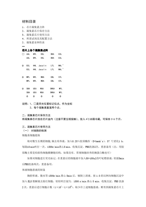
材料目录1、芯片凝集素点阵2、凝集素芯片保存方法3、凝集素芯片使用方法4、所需试剂及其配置方法5、凝集素亲和性表一芯片上各个凝集素点阵□ AAL BPL DSL DBA ECLAAL BPL DSL DBA ECLѺ EEL HHL Jacalin LTL MALΠEEL HHL Jacalin LTL MALΠѺ MPL NPL WBA EBL STLMPL NPL WBA EBL STLѺ SBA UEA WGA SWGA WFLSBA UEA WGA SWGA WFLѺѺѺѺѺ说明:1、□是荧光位置标记位点,作为坐标2、每个凝集素重复两个点。
二、凝集素芯片保存方法将凝集素芯片放在芯片盒内(注意不要互相接触),放入4℃冰箱冷藏,可保持3-6个月。
三、凝集素芯片使用方法(一)对细胞的检测细胞系细胞提取取对数生长期的细胞,倾去培养液,加入0.25%胶原酶Ⅳ(D-hank's),37 ℃消化1 h,每隔10 min吹打一次。
1500r/min离心5 min,收集沉淀。
PBS洗涤2次,重悬备用(注:用胶原酶主要是怕损伤细胞膜糖链结构,如果没有,常规细胞培养的胰蛋白酶也可)如果对细胞进行荧光标记,在重悬后的细胞液中加入50-100ul的吖啶橙溶液,轻摇5min 后PBS洗涤两次,重悬备用。
体液细胞悬液的制备胸腔积液、腹水等1500r/min离心5min后,倾倒上清液。
按1:3的比例向细胞沉淀中加入ELS裂解液去除红细胞,轻轻吹打混匀。
1500 r/min离心5 min,收集沉淀。
PBS洗涤2次,重悬后进行细胞计数(1×10⁴—1×10⁶)。
取少许上述细胞悬液,孵育到凝集素芯片上(如需荧光标记,重复上面荧光标记步骤)。
组织细胞提取取动物组织,用肝素D-hank's液清洗后剪碎,0.25%胶原酶Ⅳ(D-hank's),37℃消化1h,每隔10min吹打一次。
1500r/min离心5min,按1:3的比例向细胞沉淀中加入ELS裂解液去除红细胞,轻轻吹打混匀。
噬菌体展示技术的原理及其应用

1990年Scott等首次将随机序列肽与丝状噬菌体表面蛋 白g 融合展示在噬菌体表面,建立了噬菌体展示随机肽库。
• pVIII (50aa, ~2700 copies) • pVI (112aa, 5~8copies)
http://www.scielo.br/scielo.php?pid=S1415-47572005000100001&script=sci_artt1ex0t
载体的插入位点
11
pIII 和pVIII 噬菌体展示系统
4
特点
该技术的主要特点是将特定分子的基因型和表型统一在 同一病毒颗粒内,即在噬菌体表面展示特定蛋白质,而在噬 菌体核心DNA中则含有该蛋白的结构基因。另外,这项技术 把基因表达产物与亲和筛选结合起来,可以利用适当的靶蛋 白将目的蛋白或多肽挑选出来。
5
Phages
•Filamentous phages
• The combination of the phage and peptide is known as a Fusion Protein
13
选择方法:
淘选(Panning)
而不是
筛选(Screening)
14
非展示系统
展示系统
15
淘选系统 淘选方法
固相 完整细胞 组织,器官
常规法 正负法 竞争法
M13 Fd F1
氨基酸稳定的CdSe纳米晶对溶菌酶进行荧光标记

研究 证 明量子 点进 行表 面修 饰后 可 以作 为 生物 荧 光探 针 以来 , 越来 越 多 的 研 究 人员 对 此 又 进 行 了 广泛 而 深 入 的探 索 ] 。但 是 , 目前 较 成 熟 的 研 究 主要集 中在 有 机相 的合 成 方 法 _ 9 ’ m , 而 且 对 表 面修 饰物 的研 究也 比较 单一 , 因此 , 对 水相 中合 成 高性 能 的纳米 晶及 其在 生物 荧光 标记 中的应 用 的 研究 具有 了 重 要 的 意义 。 另外 , 所 选 用 被 标 记 的 生物 试剂 溶菌 酶 是一 种应 用相 当广 泛 的 水 解 酶 , 可 以与 细菌牢 固结 合 ( 荧 光 标 记 后有 利 于对 细 菌 结构 及作 用 机 理 的 进 一 步 研 究 ) , 并 能水 解 细 菌 细胞 壁 肽 聚糖 而 使 细 菌裂 解 死 亡 , 在生物 、 医药 、
2 实
验
以L — C y s 为稳定剂 的 C d S e纳米晶 的具体合
成 方法 与我 们 以前 的工作 相 同 ¨ , 仅对 稳 定剂 的 选用 做适 当改 变 , 本 文 主要介 绍 L — C y s稳 定 的 C d S e纳米 晶 对 溶 菌 酶 的荧 光 标 记 。用 磷 酸 缓 冲 溶液( p H约 7 . 5~8 . 0) 分 别 溶解 C d S e纳 米 晶和 溶菌酶, 将 C d S e溶液分 别 加入 到 0 . 4, 0 . 8 , 2 . 0, 3 . 0 m g / mL 的溶 菌 酶 溶 液 中 , 因溶 菌 酶 的 等 电点 约为 1 1 . 2 【 1 4 ] , 当p H值在 7 . 5左 右 时 , 表 面 带 负
马传染性贫血病毒cELISA抗体检测试剂盒技术参数
马传染性贫血病毒CELISA抗体检测试剂盒技术参数[作用与用途]本试剂盒采用竞争ELlSA技术,用于检测马血清中马传染性贫血病毒抗体,检测结果可用于马传染性贫血感染的辅助诊断。
【主要成分】______________________________________________________________________________采集待检马的血液,先将全血置37°C条件放置30分钟,后置2~8℃下放置1小时,待血清析出后收集血清。
若血清析出不佳,可将析出液以5000r∕min,离心5分钟,收集上清。
【操作方法】1 .使用前所有试剂应恢复至室温(15~25°C)o试剂应轻轻地旋转或震荡予以混合。
2 .将10倍浓缩洗涤液用双蒸水稀释10倍后备用。
3 .将待检血清样品、阴性对照血清和阳性对照血清与酶标抗原按照1:1 (V/V)混合均匀,推荐以下步骤: 吸取待检血清样品、阴性对照血清和阳性对照血清各60μl,按顺序分别加入60μl的酶标抗原,充分混匀,置37C 孵育30分钟。
4 .取出包被板,将100μl孵育后的样品加入对应的孔中,在37C孵育30分钟。
5 .弃去孔内液体,每孔加入洗涤液250μl,孵育3分钟,弃去洗涤液,洗涤4次,每次拍干。
6 .将底物溶液A和底物溶液B等体积混合均匀,作为底物溶液,现用现配。
向各反应孔中加入底物溶液100μl∕JL,置室温(15-25βC)避光显色5分钟。
7 .加入终止液,50μl∕孔,轻微震荡混合均匀后,在450nm的波长下读数(应在加入终止液后5分钟内完成读数),并记录结果。
8 .计算公式物件I虔_ ______ 阴性对照血清平均OD45θnm 值一待检血清样品OD45Onm 值____押例率二阴性对照血清平均OD450nm值一阳性对照血清平均OD45θnm值【结果判定】1 .试验结果有效的条件是:阴性对照血清的平均OD450nm值>1.0:阳性对照血清的平均OD450nm值<0.20。
生物素标签 相互作用的实验
生物素标签相互作用的实验
生物素标签是一种常用的蛋白质标记方法,可以通过生物素与亲和素的相互作用来实现蛋白质的纯化、检测和定位等操作。
以下是一些常用的生物素标签相互作用实验:
1. 亲和层析法:将生物素标记的蛋白质与亲和素柱进行层析,利用生物素与亲和素的相互作用来纯化目标蛋白质。
2. 免疫共沉淀法:将生物素标记的蛋白质与抗生物素抗体结合,再将其与含有生物素的磁珠一起加入到混合物中,利用生物素与抗生素抗体的相互作用来沉淀目标蛋白质。
3. 荧光共振能量转移法(FRET):将生物素标记的蛋白质与荧光标记的亲和素结合,利用生物素与亲和素的相互作用来实现荧光共振能量转移,从而检测蛋白质相互作用。
4. 免疫荧光染色法:将生物素标记的蛋白质与荧光标记的抗生物素抗体结合,利用生物素与抗生素抗体的相互作用来定位目标蛋白质在细胞中的位置。
以上是一些常用的生物素标签相互作用实验,可以根据实验需要选择
合适的方法进行操作。
WaferBacksideCoatingOfDie

For decades the semiconductor industry has used adhesive pastes to attach die to leadframes and other substrates. Typically, adhesive has been dispensed through needles from syringes, or for smaller dots, applied by the pin-transfer method. Some manufacturers, notably in the automotive hybrid industry, have applied adhesive by screen printing. What’s the problem?Actually, there are several problems.Speed. In the highly competitive semiconductor industry, time is money. In some cases, dispensing adhesives may be a limiting factor in the production rate. If adhesive can be applied faster, then production lines run faster and costs can be reduced. In principle there are ways to speed up the dispense process,but none has made much impact thus far.Size. With traditional paste die attach, the adhesive forms a fi llet around the chip. This is a useful visual indicator to con fi rm that suf fi cient adhesive has been applied. It also increases the die shear strength by supporting the side of the die. However, the fi llet effectively increases the footprint area of the chip, which means that any packaging must be slightly larger than the die itself. This extra area can be quite substantial after adding the tolerances that account forvariations in fi llet size due to differences inpaste volume, fl ow, and misplacement of paste and die. Since all paste adhesives are prone to resin bleed, space must be left to ensure that surrounding bond pads are not affected by excessive bleed.Quality/Reliability. Placing a chip into a dot of adhesive paste is a delicate operation. The force and time must be controlled to ensure that the adhesive has completely covered the underside of the die, yet the force must not be so high that the adhesive is squeezed from the bondline. Level placement of the chip is also extremely important. Any residual tilt may hamper the wirebonding process or impact reliability by creating regions of high stress where the bondline is thinnest. In addition, any lack of control of the above parameters can impact short or long-term reliability.What’s Changed?As designers try to make packages smaller and thinner, and as manufacturing plants try to reduce costs by speeding up assembly, all the above issues become increasingly important. Often solving one problem only makes another one worse. For example, die tilt variations may be solved with a higher speci fi cation die bonder, but this may not be cheaper or run at higher speed than the existing bonder.Another trend is to place more than one chip inside a package. These can sit side by side, in which case determination of the proper adhesive will permit optimal spacing of the dice. Alternatively chips can be stacked on top of each other. Here the dice are usually very thin, and so tight control of fi llet heights is essential to prevent adhesive from contaminating the die surface.Wafer Backside Coating Of Die Attach Adhesives New Method Simpli fi es Process, Saves MoneyBy Tony Winster, Craig Borkowski, and Alan HobbyFigure 1. High-speed die bonder dispenses adhesiveClearly an alternative to traditional paste adhesive application would be attractive. One solution already in place is to use adhesive in the form of a dry fi lm. This is supplied at a controlled thickness. It can either be punched into preforms or applied to the back of a silicon wafer before dicing into individual die. When each die is picked, it carries its own adhesive with it to the leadframe or substrate. Some heat and pressure are needed to attach the adhesive to the leadframe, but the adhesive remains suf fi ciently hard to prevent the formation of large fi llets and to prevent any signi fi cant die tilt.This approach is widely used in die-stacking applications, where cost is not yet a major factor. Unfortunately the cost of manufacturing and packaging a fi lm is higher than a paste. Thus, this approach is dif fi cult to implement in very high volume, cost-sensitive applications What’s the Solution?One very practical solution is wafer backside coating (WBC). In WBC the adhesive is supplied as a speci fi cally designed paste, which is applied to the back of a wafer and dried. This method leads to a number of extremely desirable practical advantages. These include:• Paste is 20-30% cheaper than fi lm• Bondline thickness can be controlled tocustomer specs• Fillet control is very similar to that of a fi lmproduct• Dispense operation is eliminated, whichaffords higher units per hour (UPH)• Coated wafer can be stored until required As shown below in Figure 3, the wafer can be attached to conventional dicing tape and diced with standard saws. The only modi fi cation that may be required to a standard die bonder is to fi t a heater under the stage to ensure that the adhesive softens suf fi ciently to wet the surface.What’s Needed to Print the Adhesive?The adhesive can be applied quickly using a screen-printing platform such as those used in surface-mount production lines to depositsolder pastes. The platforms are readilyFigure 2. Screen or stencil printing can be used to coat the backside of semiconductor wafers in preparation forcuring and subsequent die attachFigure 3. Schematic of WBC Process Routeavailable at reasonable cost and deliver sufficient accuracy and repeatability to enable complete coverage of the wafer with minimal waste.Using such a printer, a concentric adhesive layer can be deposited on the wafer backside with little variation in thickness. The entire process typically takes 10-15 seconds to complete, using a suitable combination of stencil and squeegee. An emulsion screen may provide a suitable alternative to a metal stencil, depending on the adhesive characteristics. Automated wafer loaders/unloaders have also been developed to support wafer-level, screen/ stencil printing processes. Available units are compatible with wafers in all standard sizes upto 300mm and larger. These integrate directly with standard wafer-storage formats such as JEDEC cassettes or front-opening universal pods, which are widely used throughout the semiconductor-processing industry. After unloading the coated wafer, it can be returnedto the cassette/pod or transported directly into the curing oven. A typical loader/unloader uses industry-standard SMEMA protocols to communicate with related equipment.The design and construction of suitable stencils have been adapted from technology developed in the surface-mount industry. Highly satisfactory results have been achieved usinga stainless steel stencil with a single, large aperture. The effectiveness of stencils as thin as 37 microns has been achieved. A purpose-designed squeegee, which is very rigid to avoid scooping adhesive out of the aperture as it passes, produces a thin and uniform coating. Modifications to the tooling and handling mechanisms of a standard printer enable wafer backside coating. These include tooling revisions to support extremely thin wafers. The wafer must remain very flat throughout the process in order to prevent excessive variationsin the thickness of the adhesive layer. A pallet, having comparable flatness to a surface plate for metrology applications, is used to hold the wafer. A vacuum is applied to the wafer through porous ceramic inserts in the pallet to hold the wafer without incurring damage.Non-contact measuring equipment can accurately measure the thickness of the adhesive layer, but is not suitable for rapid inspection of each wafer in a volume production environment. Thus, after calibrating the process using a profi lometer, it is most practical to test samples at regular intervals during production. Once correctly set up, there is no reason for the process to vary widely, since screen or stencil printing equipment and processes are very robust. A complete turnkey system, including printer, wafer handler, and inline oven costs about $320,000 and provides a throughput of 60-85 wafers per hour (UPH), based on the useof an 203 mm wafer.Figure 4. Screen or stencil printer used in Wafer Backside Coating applications Figure 5. Wafer pallet featuring porousvacuum insertsWhat Are the Additional Benefi ts?In addition to the solutions to the basic problems outlined above, WBC also affords additional benefi ts. These include:• Reduction of paste adhesive volume by a factor of ten on die less than 0.5 x 0.5 mm by eliminating the fi llet.• Improved inventory control by concentrating the application of wet adhesive in a dedicatedprint area within the user’s facility. This also reduces the need for expensive engineering and safety controls where chemicals are being handled. In fact, it may be possible to print the adhesive at the wafer fab facility, thus eliminating the need to handle wet paste adhesives in the packaging or "back-end" facility.• Additional inventory control advantages because only one paste formulation satisfi es every need rather than the multiple thicknesses and widths currently necessary with fi lms.What Is the Status of WBC?First generation WBC products are currently available in both electrically conductive and electrically insulating versions. Second generation materials with improved printability and thermal properties will be available this year. In parallel with materials development, improvements are being made in wafer handling to allow faster throughputs and to enable processing of thinner wafers. In fact, 150 mm wafers that are just 30 microns thick have been successfully coated. Thus, current indications are that, as the process is improved even further, wafer backside coating will take its place in the pantheon of standard semiconductor processing.Author ContactsTony Winster, Ablestik UK (+44 1223 893771) e-mail: *************************Craig Borkowski, Ablestik USA (+1 310-764-4600) e-mail : **************************** Alan Hobby, DEK UK (+44 1305 760760)e-mail: **************。
荧光抗体标记_实验报告
一、实验目的1. 掌握荧光抗体标记技术的基本原理和操作步骤。
2. 学会使用荧光显微镜观察荧光标记的抗体与抗原的结合情况。
3. 了解荧光抗体标记技术在生物医学研究中的应用。
二、实验原理荧光抗体标记技术是将荧光素与特异性抗体结合,形成荧光标记抗体。
这种标记抗体仍保持抗体原有的活性,当与相应的抗原发生特异性结合时,荧光标记抗体在荧光显微镜下呈现出明亮的荧光,从而实现对抗原的检测和定位。
三、实验材料1. 实验试剂:FITC标记的抗体、抗原、抗体稀释液、磷酸盐缓冲液(PBS)、甘油、甲醇等。
2. 实验仪器:荧光显微镜、离心机、移液器、吸管、试管、载玻片等。
四、实验步骤1. 标准化抗体将FITC标记的抗体用抗体稀释液稀释至适当浓度。
2. 制备抗原将待检测的抗原用磷酸盐缓冲液(PBS)稀释至适当浓度。
3. 制备细胞悬液将待检测的细胞用磷酸盐缓冲液(PBS)洗涤后,离心弃去上清液,加入适量的磷酸盐缓冲液重悬细胞。
4. 混合抗原与抗体将抗原与抗体按一定比例混合,在室温下孵育一段时间。
5. 洗涤将混合后的溶液在室温下用磷酸盐缓冲液洗涤3次,每次洗涤后离心弃去上清液。
6. 封片将洗涤后的细胞沉淀用甘油封片,封片剂与细胞沉淀的比例为1:1。
7. 荧光显微镜观察将封片置于荧光显微镜下观察,调整显微镜参数,观察荧光标记的抗体与抗原的结合情况。
五、实验结果通过荧光显微镜观察,发现荧光标记的抗体与抗原发生了特异性结合,形成明亮的荧光复合物。
阳性细胞在荧光显微镜下呈现出明显的荧光信号,而阴性细胞则无荧光信号。
六、实验讨论1. 实验过程中,抗体与抗原的孵育时间、洗涤次数和封片剂的选择对实验结果有较大影响。
本实验中,抗体与抗原的孵育时间为30分钟,洗涤次数为3次,封片剂为甘油。
2. 荧光抗体标记技术具有特异性高、灵敏度高、操作简便等优点,广泛应用于生物医学研究、临床诊断等领域。
3. 在实验过程中,应注意以下几点:(1)抗体与抗原的比例要适中,过多或过少都会影响实验结果;(2)孵育时间不宜过长或过短,以免影响抗体与抗原的结合;(3)洗涤时要充分,以去除未结合的抗体和抗原;(4)封片剂的选择要合适,以保证荧光信号的稳定。
Prog.+Photovolt-+Res.+Appl.+2007,15,603–612

Research Fabrication of Screen-PrintingPastes From TiO 2Powders forDye-Sensitised Solar CellsSeigo Ito,Peter Chen,Pascal Comte,Mohammad Khaja Nazeeruddin,Paul Liska,Pe´ter Pe ´chy and Michael Gra ¨tzel *y Laboratory of Photonique and Interfaces (LPI),Institute des Sciences et Ingenierie Chimiques (ISIC),E´cole Polytechnique Fe´de ´rale de Lausanne (EPFL),CH-1015Lausanne,Switzerland A preparation technique of TiO 2screen-printing pastes from commercially-availablepowders has been disclosed in order to fabricate the nanocrystalline layers withoutcracking and peeling-off over 17m m thickness for the photoactive electrodes of thedye-sensitised solar cells.A conversion efficiency of 8Á7%was obtained by using asingle-layer of a semi-transparent-TiO 2film.A conversion efficiency of 9Á2%wasobtained by using double-layers composed of transparent and light-scattering TiO 2films for a photon-trapping system.Copyright #2007John Wiley &Sons,Ltd.key words :titanium dioxide;nanocrystalline electrode;dye-sensitised solar cellsReceived 9January 2007;Revised 20March 2007INTRODUCTIONDye-sensitised solar cells (DSCs)are currently attracting academic and commercial interest as regenerative low-cost alternatives to conventional solid state devices.1,2So far,the best performing nanocrystalline-TiO 2electrodes have been fabricated by hydrothermal autoclaving and screen-printing deposition.3–5Screen-printing of TiO 2is a widespread industrially-applied method because of the fast-printing technique and of the coating facility with fine controlling of the position and thickness.Other applied fields are gas sensors (humidity,O 2,H 2,NO X ,CH X ,CO,etc.),ion sensors,piezoelectric devices,microfiltration membranes,Gamma-radiation sensors,electroluminescent devises,electrochromic display,antireflection coatings on silicon solar cells,microwave applications,photocatalyst coatings and so on.The nontoxicity of titanium dioxide,which is used in paints,cosmetics and health care products,adds advantages to the fields.The key point on the screen-printing is the quality and characteristics of TiO 2paste.For the best-performing TiO 2electrodes,the synthesis of TiO 2paste involves hydrolysis of Ti(OCH(CH 3)2)4in water at 2508C (70atms)for 12h,followed by conversion of the water to ethanol by three-times centrifugation.Finally,the ethanol is exchanged with a -terpineol by sonication and evaporation.3Totally,it takes 3days.Such a long-time procedure of TiO 2pastes is economically unsuitable for industrial production and has to be reduced.Towards this goal,several reports were published in order to fabricate screen-printing paste from a commercially-available TiO 2powder (P25,Degussa).6–9Most of the pastes were based on water and alcohols,which induce TiO 2aggregation and yielding poorly reproducible results in long-term experiments.On the other hand,a -terpineol-based PROGRESS IN PHOTOVOLTAICS:RESEARCH AND APPLICATIONSProg.Photovolt:Res.Appl.2007;15:603–612Published online 30May 2007in Wiley InterScience ()DOI:10.1002/pip.768*Correspondence to:Michael Gra ¨tzel,Laboratory of Photonique and Interfaces (LPI),Institute des Sciences et Ingenierie Chimiques (ISIC),E ´cole Polytechnique Fe ´de ´rale de Lausanne (EPFL),CH-1015Lausanne,Switzerland.y E-mail:michael.graetzel@epfl.chCopyright #2007John Wiley &Sons,Ltd.604S.ITO ET AL. pastes3–5are very stable at long-term and give very reproducible results for several years.However,a reported paste made from P25and a-terpineol did not give better DSCs than that of a water-based paste.9In this study,we have developed a new procedure which takes only4h to produce TiO2pastes with a-terpineol from commercially-available powders,resulting in DSCs with ca.9%conversion efficiencies. Moreover,the most important point of this work is to utilise the commercially-available TiO2particles for the high-efficiency DSCs,because the synthesis of the homemade TiO2particle demands the delicate techniques and consequently the different batch of TiO2particle might give different results.For the reproducible results, therefore,it is important to investigate a new fabrication method of TiO2paste from commercially-available particles.This report will be of great help for the people who are engaged with DSCs. EXPERIMENTALMaterialsThree kinds of commercially-available TiO2powders were used:P25(av.30nm by Brunauer-Emmett-Teller (BET),80%anatase(d¼21nm)and20%rutile(d¼50nm),via TiCl4-fumed gas synthesis,Degussa, Germany);ST21(av.25nm by BET,100%anatase,via sulfuric-acid synthesis,Ishihara Sangyo,Japan);ST41 (av.160nm by BET,100%anatase,via sulfuric-acid synthesis,Ishihara Sangyo,Japan).Two kinds of pure powders of ethyl celluloses(5–15mPas at5%in toluene:ethanol/80:20at25oC,#46070,Fluka;30–50mPas at 5%in toluene:ethanol/80:20at258C,#46080,Fluka)were dissolved beforehand in an ethanol solution(these powders of ethyl cellulose don’t contain toluene and ethanol which were mixed with ethyl cellulose just to show the specification results of viscosity).Each concentration of the ethyl cellulose was5wt%:the total amount of ethyl celluloses was10wt%in ethanol.4-tert-butylpyridine(Aldrich),acetonitrile(Fluka)and valeronitrile(Fluka)were purified by vacuum distillation.Guanidinium thiocyanate(Aldrich)and H2PtCl6(Fluka)were used as received.H2O was purified by distillation andfiltration(Milli-Q).TiCl4(Fluka)was diluted with water to2M at08C to make a stock solution, which was kept in a freezer and freshly diluted to40mm with water for each TiCl4treatment of the F-doped tin oxide(FTO)coated glass plates.Iodine(99Á999%,Superpur1,Merck)was used as received.The synthesis of cis-di(thiocyanato)-N,N’-bis(2,2’-bipyridyl-4-carboxylic acid-4’-tetrabutylammonium carboxy late)ruthenium (II)(N-719)and butylmethylimidazolium iodide(BMII)were reported in our previous paper.10,11The chromatographic purification of N-719was carried out three times on a column of Sephadex LH-20using the following procedure.4,5Preparation of TiO2pasteThe fabrication scheme for TiO2pastes was described in Figure1.At each step,liquids were added drop by drop into an alumina mortar,which is more stable than a porcelain one.The diameter of the mortar was ca.20cm.The condition was in the ambient air at room temperature.The TiO2powders stuck on the inside of the mortar should be removed by a plastic spatula in order to grind large aggregates.The TiO2dispersions in the mortar were transferred with excess of ethanol(100ml)to a tall beaker and stirred with a4cm long magnet tip at300rpm. The ultrasonic homogenisation was performed with using a Ti-horn-equipped sonicator(Vibra cell72408, Bioblock scientific).Anhydrous terpineol(Fluka)and the mixture solution of two ethyl celluloses in ethanol were added,followed by stirring and sonication.The contents in dispersion were concentrated by evaporator at 358C with120mbar atfirst.The pressure was evacuated until10mbar.The pastes werefinalised with a three-roller-mill grinder(EXAKT).In this scheme(Figure1),the coexistence of water and acetic acid was important.We tried another combination with nitric acid,hydrochloric acid,acetyl acetone,polyethylene glycol,triton X-100and so on. Without water and/or acetic acid,however,the porous-TiO2layers over10m m thickness were mechanically unstable and did not keep the structure after sintering due to the large cracks and peeling-up from substrate. Copyright#2007John Wiley&Sons,Ltd.Prog.Photovolt:Res.Appl.2007;15:603–612DOI:10.1002/pipWe speculate the reason as below.In order to make a good connection between TiO 2particles and between a TiO 2particle and SnO 2surface,hydroxides (–OH)have to be on the surface and make strong chemical bonding between each other by dehydration at sintering:M 1ÀOH þHO ÀM 2!M 1ÀO ÀM 2þH 2Owhere,M 1shows a titanium atom on a surface of a particle and M 2shows a titanium atom of another particle or a tin atom on a plate of transparent conductive oxide (TCO)substrate (F-doped tin oxide (FTO)glass).The water added at first can make the surface covered by hydroxides.At the same time,each particle has to be isolated from each other and not to be aggregated.The aggregates in matrix can make large shrinkage of the film at the sintering,resulting in the peering-off from the TCO substrate.The acetic acid can be adsorbed on the surface of TiO 2and prohibits each particle from the aggregation.At the same time,the proton (H þ)of acid can also be adsorbed on the surface and shifts the Zeta potential to positive,resulting in repelling the particles from each other.About the reproducibility,as long as the timing of adding,mixing and grinding the materials in the mortar is kept up,the result is quite reproducible (the data was not shown).However,by changing the timing,it can change.For example,if we add all of the ethanol in one time,it is very difficult to remove the aggregate.The paste can be a film peeled-off from the substrate or be a DSC electrode with a low photovoltaic efficiency.Preparation of nanocrystalline-TiO 2electrodesTo prepare the DSC working electrodes,the FTO glass used as current collector (Solar 4mm thickness,10V /&,Nippon Sheet Glass,Japan)was first cleaned in a detergent solution using an ultrasonic bath for 15min,and then rinsed with water and ethanol.After treatment in a UV-O 3system (Model No.256–220,Jelight Company,Inc.)for 18min,the FTO glass plates were immersed into a 40mm aqueous TiCl 4aqueous solution at 708C for 30min and washed with water and ethanol.A layer of paste was coated on the FTO glass plates by screen-printing (90T,Estal Mono,Schweiz.Seidengazefabrik AG Thal),kept in a clean box for 3min with ethanol so that the paste can relax to reduce the surface irregularity and then dried for 6min at 1258C.The screen characteristics areas Figure 1.Fabrication scheme of screen-printing paste from a nanocrystalline-TiO 2powderCopyright #2007John Wiley &Sons,Ltd.Prog.Photovolt:Res.Appl.2007;15:603–612DOI:10.1002/pipFABRICATION OF SCREEN-PRINTING PASTES 605606S.ITO ET AL. follows:material,polyester;mesh count,90T mesh/cm(or230T mesh/inch);mesh opening,60m m;thread diameter,50m m;open surface,29Á8%;fabric thickness,83m m;theoretical paste volume,24Á5cm3mÀ2;K/KS volume,17Á0cm3mÀ2;weight,48g mÀ2.This screen-printing procedure(with coating,storing and drying)was repeated to change the thickness of the nanocrystalline-TiO2working electrode.For the single-layer electrode, the TiO2paste of ST21was used,resulting in a light-scatteringfilm.For the double-layer electrode,the paste of P25for the transparent layer was coated by screen-printing and dried at1258C,and then,the second layers of ST41for the light-scattering layer were deposited by screen-printing to4–5m m thickness.The electrodes coated with the TiO2pastes were gradually heated under an airflow at3258C for5min,at3758C for5min,at4508C for 15min and5008C for15min8C.After sintering,the surface area of the TiO2electrodes was measured precisely by a scanner with600dpi resolution in grey mode,followed by integration of the resulting image.4DSC assemblingAfter the size measurement,the TiO2film was treated with40mm TiCl4solution as described above,rinsed with water and ethanol and sintered at5008C for30min.At808C in the cooling,the TiO2electrode was immersed into a0Á5mM N-719dye solution in a mixture of acetonitrile and tert-butyl alcohol(volume ratio:1:1)and kept at room temperature for20–24h to complete the sensitiser uptake.To prepare the counter electrode,a hole was drilled in the FTO glass(LOF Industries,TEC15V/&,2Á2mm thickness)by sand blasting.The perforated sheet was washed with H2O as well as with a0Á1M HCl solution in ethanol and cleaned by ultrasound in an acetone bath for10min.After removing residual organic contaminants by heating in air for15min at4008C,the Pt catalyst was deposited on the FTO glass by coating with a drop of H2PtCl6solution(2mg Pt in1ml ethanol)and repeating the heat treatment at4008C for15min.The dye-covered TiO2electrode and Pt-counter electrode were assembled into a sandwich type cell and sealed with a hot-melt gasket of25m m thickness made of the ionomer Surlyn1702(Dupont).The aperture of the Surlyn frame was2mm larger than that of the TiO2area and its width was1mm.A drop of the electrolyte,a solution0Á60M BMII,0Á03M I2,0Á10M guanidinium thiocyanate and0Á50M4-tert-butylpyridine in the mixture of acetonitrile and valeronitrile(volume ratio:85:15))was put on the hole in the back of the counter electrode.The electrolyte was introduced into the cell via vacuum backfilling.The cell was placed in a small vacuum chamber to remove inside air.Exposing it again to ambient pressure causes the electrolyte to be driven into the cell.Finally,the hole was sealed using a hot-smelt ionomerfilm(Bynel4702,35m m thickness,Du-Pont) and a cover glass(0Á1mm thickness).Photovoltaic measurement of DSCLight reflection losses were eliminated using a self-adhesivefluorinated polymerfilm(ARKTOP,ASAHI GLASS)that served at the same time as a380nm UV cut-offfilter.Photovoltaic measurements employed an AM 1Á5solar simulator.The power of the simulated light was calibrated to be100mW cmÀ2by using a reference Si photodiode equipped with an IR-cutofffilter(KG-3,Schott),which was calibrated at three solar-energy institutes(ISE(Germany),NREL(USA),SRI(Switzerland)).4I-V curves were obtained by applying an external bias to the cell and measuring the generated photocurrent with a Keithley model2400digital source meter.The voltage step and delay time of photocurrent were10MV and40ms,respectively.RESULTS AND DISCUSSIONMorphology of screen-printed TiO2filmsFigure2shows SEM pictures of porous TiO2films.We can notice that the particles of P25contained small particles(anatase,20nm)and large particles(rutile,40nm).Compared with the pictures of TiO2films made via Copyright#2007John Wiley&Sons,Ltd.Prog.Photovolt:Res.Appl.2007;15:603–612DOI:10.1002/pipcolloidal synthetic routes (Figure 2g and h),the P25film contained no aggregates (Figure 2a),and was dispersed homogeneously over the large area (Figure 2b).On the other hand,ST21showed the small aggregates (ca .100nm,Figure 2c)and the large aggregates (micron-meter order,Figure 2d).The large aggregates of ST21were very difficult to be broken by this procedure and gave small cracks in the porous TiO 2layer (Figure 2d).The difference of the morphologies between P25and ST21was due to the synthesis method:fumed-TiCl 4and sulphuric-acid routes,respectively.ST41contained 50–200nm large particles (Figure 2e).The average was 160nm from BET data (measured by Ishihara Sangyo).Although ST41also was made by the sulphuric-acid synthesis,this layer was homogeneous over the large area (Figure 2f).Hence,the aggregations between ST41particles did not affect the surface morphology on a large scale.For the comparison with homemade TiO 2,we added the SEM pictures (Figure 2g and h).Although the aggregates about 200nm existed (in a white circle of Figure 2g)and we can find small dots in Figure 2h from the aggregate,the surface was very smooth and uniform over the large area (Figure 2h).Figure 3shows cross sections of nanocrystalline-TiO 2layers by surface-profiling method (Alphastep 550).Each layer was the single screen-printing using a 90T mesh.The layer of P25and ST41was relativelyflat Figure 2.SEM photographs of porous TiO 2films showing the surface morphology of P25(a,b),ST21(c,d),ST41(e,f)andhomemade TiO 2(d ¼20nm)(g,h)with two types of magnification:120000Â(a,c,e,g)and 5000Â(b,d,f,h)Copyright #2007John Wiley &Sons,Ltd.Prog.Photovolt:Res.Appl.2007;15:603–612DOI:10.1002/pipFABRICATION OF SCREEN-PRINTING PASTES 607compared with that of ST21.This phenomenon reflected the morphology which was observed by SEM (Figure 2).The flatness of P25and ST41layers reflect the homogeneous dispersion of particles.On the other hand,the roughness of ST21layer reflects the aggregations (Figure 2d).Figure 4a shows the photograph of screen-printed layers with a background of garden plants.The P25film was transparent and pale blue.We can see the clear image of the background.The ST21film was semi-transparent and we can see slightly the images of background.The ST41was opaque and completely white and we cannot see any images through the film.Figure 4b shows the transmittance spectra of screen-printed TiO 2layers used in Figures 3and 4a.The P25layer transmitted 60%of incident light above 480nm wavelength and diffused the shorter wavelength effectively.Therefore,the P25layer was pale blue (Figure 4a).The transmittance of ST21increased linearly from 378to 820nm wavelength,and the transmittance at 820nm was half that of P25.ST41blocked the incident light below 600nm wavelength and let the incident light slightly through above that.For the comparison with homemade TiO 2,we added the data of transmission,which shows the higher transparency of the homemade TiO 2layer than those of commercially-available TiO 2powders.However,if 100%-anatase nanoparticles made by fumed-TiCl 4synthesis is available,more highly-transparent TiO 2layer can be fabricated.It has been reported that particles over 100nm can diffuse visible light effectively.12–14Hence,ST41(av.160nm)was able to diffuse visible light.This is the reason why the layer of ST41was white and opaque (Figure 4).On the other hand,the particle sizes of P25(av.21nm)and ST41(av.20nm)were close.Hence,the optical difference between layers of P25(transparent)and ST21(hazy)(Figure 4)arises from the aggregates and the roughness,acting as light-scattering centres (Figures 2and 3).The difference of morphologies was due to the synthetic variation:a liquid-phase synthesis for ST21and a gas-fumed synthesis forP25.Figure 3.Cross sections of nanocrystalline-TiO 2layers by surface-profiling method (Alfastep550):P25(a),ST21(b)andST41(c)Copyright #2007John Wiley &Sons,Ltd.Prog.Photovolt:Res.Appl.2007;15:603–612DOI:10.1002/pip608S.ITO ET AL.DSC Photovoltaics related with thickness of nanocrystalline-TiO 2electrodesIn order to fabricate DSCs,the TiO 2pastes were coated by screen-printing on FTO/glass substrates and assembled to DSC.For the high-efficiency DSC,therefore,we applied P25and ST41to transparent and light-scattering layers in double-layer photon-trapping system as reported,respectively.3–5Since the ST21layer was semi-transparent,we cannot expect the optical merit for applying the ST21layer to the double-layer photon-trapping system.Therefore,the ST21layer was used in DSC electrodes as a single layer.Figure 5shows the relationships between the screen-printing times and the thickness of nanocrystalline-TiO 2(P25and ST21)layers,which were used for DSC electrodes (Figures 5and 6).The ‘P25þST41’and ‘ST21’layers were double-layer and single-layer structures,respectively,as written in the previous paragraph.The thickness of ST41was fixed at 5Á7m m,which was obtained by the interception of y -axis.The linear relationship between the coating time and the thickness was confirmed.The thicknesses of one screen-print coating of P25and ST21were obtained as 1Á9m m and 2Á0m m,respectively.Each paste gave a thick layer over 17m m without cracking and peeling-up at the exterior;nanoscale cracks in the ST21layer were observed by SEM (see Figure 2d).Figure 6shows the photovoltaic-characteristic variations of open-circuit photo voltage (a,V OC ),short-circuit photo current density (b,J SC ),fill factor (c,FF)and conversion efficiency (d,h ).The V OC and FF decreased linearly with increasing thickness,but the changing ratios were just 10%and 2%,respectively (Figure 6a and c).On the other hand,J SC of P25-ST41and ST21increased by 30%and 50%,respectively (Figure 6b),which Figure 4.A picture (a)and transmittance spectra (b)of screen-printed nanocrystalline-TiO 2layers.The transmittance measurements were performed with cover glass plates which were attached on the surface of TiO 2layer,and the pores in nanocrystalline-TiO 2layers were filled with butoxyacetonitrile to decrease the light-scattering effect.The optical background for (b)was obtained by using the same FTO/glass substrate,butoxyacetonitrile and the cover glass plate Copyright #2007John Wiley &Sons,Ltd.Prog.Photovolt:Res.Appl.2007;15:603–612DOI:10.1002/pipFABRICATION OF SCREEN-PRINTING PASTES 609projects the variation of h (Figure 6d).Resulting efficiencies of double-layer (P25-ST41)and single-layer (ST21)electrodes had peaks at 14and 17m m thickness of nanocrystalline layers (P25and ST21),respectively (Figure 6d).Figure 7shows photo I-V curves of best efficiency DSCs using P25-ST41and ST21.The photovoltaic characteristics were J SC ¼16Á25mA cm À2,V OC ¼779mV,FF ¼0Á730,and h ¼9Á24%with P25-ST41and J SC ¼15Á3mA cm À2,V OC ¼778mV ,FF ¼0Á733,and h ¼8Á75%with ST21.These efficiencies are the best results published ever with using commercially-available TiO 2powders.Figure 5.Relationship between number of coating times and thickness of screen-printed nanocrystalline-TiO 2layers of P25þST41and ST21.In P25þST41,the thickness of P25was varied and that of ST41was fixed at 5Á7m m by two-timesscreen printing for utilisation of photovoltaic measurements in Figures 6and7Figure 6.Photovoltaic-characteristics relationship with nanocrystalline (P25and ST21)-layer thickness of P25þST41(*)and ST21(&)electrodes:V OC (a),J SC (b),FF (c)and conversion efficiency (h )(d).The thickness of ST41was fixed at 5Á7m m for the light-scattering layer.The solid and doted lines were fitted to the average data of P25þST41and ST21,respectivelyCopyright #2007John Wiley &Sons,Ltd.Prog.Photovolt:Res.Appl.2007;15:603–612DOI:10.1002/pip610S.ITO ET AL.CONCLUSIONIn summary,this screen-printing technique enabled the fabrication of nanocrystalline layers over 17m m thickness from commercially-available TiO 2powders.The result of 9Á2%efficiency was lower than that from our homemade double-layered electrode (10–11%).4,5However,this report shows the best efficiencies using commercially-available TiO 2powders,which is very important for the world-wide market production of solar cells.Since P25and ST21contained rutile particles and large aggregates,respectively,the efficiencies were lower than 10%.If we can get more transparent electrodes using 100%-anatase nanoparticles made by fumed-TiCl 4synthesis,more highly efficient photovoltaic DSC can be fabricated.We believe that this report can be of great help for the DSC researchers.The results of this study imply that using TiO 2powders of a large commercial batch instead of TiO 2particles of homemade small different batches result in a more reproducible cell efficiency.This methodological investigation can contribute not only to the research of DSC,but also to various applications of industrial and scientific works in several fields as suggested in the introduction.AcknowledgementsWe acknowledge financial support of this work by the Swiss Science Foundation and Swiss Federal Office for Energy (OFEN).Peter Chen thanks the Taiwan Merit Scholarships Program (TMS-094-2A-026).The SEM-image works were carried out in the CIME of EPFL.REFERENCES1.O’Regan B,Gra¨tzel M.A low cost,high-efficiency solar cell based on dye-sensitized colloidal TiO 2films.Nature (London)1991;353:737–739.2.Gra¨tzel M.Photoelectrochemical cells.Nature (London)2001;414:338–344.3.Wang P,Zakeeruddin SM,Comte P,Charvet R,Humphry-Baker R,Gratzel M.Enhance the performance of dye-sensitized solar cells by co-grafting amphiphilic sensitizer and hexadecylmalonic acid on TiO 2nanocrystals.Journal of Physical Chemistry B 2003;107:14336–14341.4.Ito S,Nazeeruddin MK,Liska P,Comte P,Charvet R,Pe´chy P,Jirousek M,Kay A,Zakeeruddin SM,Gratzel M.Photovoltaic characterization of dye-sensitized solar cells:effect of device masking on conversion efficiency.Progress in Photovoltaics 2006;14:589–601.Figure 7.Photo I-V curves of best-efficiency dye-sensitised solar cells using nanocrystalline-TiO 2electrodes fabricated from commercially-available nanocrystalline-TiO 2powders (P25þST41,h ¼9Á24%;ST21,h ¼8Á75%)under100mW cm À2AM 1Á5irradiationCopyright #2007John Wiley &Sons,Ltd.Prog.Photovolt:Res.Appl.2007;15:603–612DOI:10.1002/pipFABRICATION OF SCREEN-PRINTING PASTES 611612S.ITO ET AL.5.Nazeeruddin Md K,De Angelis F,Fantacci S,Selloni A,Viscardi G,Liska P,Ito S,Takeru B,Gra¨tzel binedexperimental and DFT-TDDFT computational study of photoelectrochemical cell ruthenium sensitizers.Journal of the American Chemical Society2005;127:16835–16847.6.Tsoukleris DS,Arabatzis IM,Chatzivasiloglou E,Kontos AI,Belessi V,Bernard MC,Falaras P.2-Ethyl-1-hexanol basedscreen-printed titania thinfilms for dye-sensitized solar cells.Solar Energy2005;79:422–430.7.Zhang D,Ito S,Wada Y,Kitamura T,Yanagida S.Nanocrystalline TiO2electrodes prepared by water-medium screenprinting technique.Chemistry Letters2001;30:1042–1043.8.Gupta TK,Cirignano LJ,Shah KS,Moy LP,Kelly DJ,Squillante MR,Entine G,Smestad GP.Screen-printeddye-sensitized large area nanocrystalline solar cell.Material Research Society Symposium Proceedings2000;581: 653–658.9.Ma T,Kida T,Akiyama M,Inoue K,Tsunematsu S,Yao K,Noma H,Abe E.Preparation and properties ofnanostructured TiO2electrode by a polymer organic-medium screen-printing technique.Electrochemistry Communi-cations2003;5:369–372.10.Nazeeruddin MK,Zakeeruddin SM,Humphry-Baker R,Jirousek M,Liska P,Vlachopoulos N,Shklover V,Fischer CH,Gra¨tzel M.Acid-base equilibria of(2,2’-Bipyridyl-4,4’-dicarboxylic acid)ruthenium(II)complexes and the effect of protonation on charge-transfer sensitization of nanocrystalline titania.Inorganic Chemistry1999;38:6298–6305. 11.Bonhoˆte P,Dias AP,Armand M,Papageorgiou N,Kalyanasundaram K,Gra¨tzel M.Hydrophobic,highly conductiveambient-temperature molten salts.Inorganic Chemistry1996;35:1168–1178.12.Rothenberger G,Comte P,Gra¨tzel M.A contribution to the optical design of dye-sensitized nanocrystalline solar cells.Solar Energy Materials and Solar Cells1999;58:321–336.13.Tachibana Y,Hara K,Sayama K,Arakawa H.Quantitative analysis of light-harvesting efficiency and electron-transferyield in ruthenium-dye-sensitized nanocrystalline TiO2solar cells.Chemistry of Materials2002;14:2527–2535. 14.Ito S,Yoshida S,Watanabe T.Preparation of Colloidal Anatase TiO2Secondary Submicroparticles by HydrothermalSol-Gel Method.Chemistry Letters2000;29:70–71.Copyright#2007John Wiley&Sons,Ltd.Prog.Photovolt:Res.Appl.2007;15:603–612DOI:10.1002/pip。
大鼠维生素D(VD)ELISA试剂盒操作说明

大鼠维生素D(VD)ELISA试剂盒操作说明大鼠维生素D(VD)ELISA试剂盒操作说明大鼠维生素D(VD)ELISA试剂盒实验原理大鼠维生素D(VD)ELISA试剂盒采用双抗体一步夹心法酶联免疫吸附试验(ELISA)。
往预先包被大鼠维生素D(VD)捕获抗体的包被微孔中,依次加入标本、标准品、HRP标记的检测抗体,经过温育并彻di洗涤。
用底物TMB显色,TMB在过氧化物酶的催化下转化成蓝色,并在酸的作用下转化成最终的黄色。
颜色的深浅和样品中的大鼠维生素D(VD)呈正相关。
用酶标仪在450nm 波长下测定吸光度(OD 值),计算样品浓度。
样本处理及要求1. 血清:将收集于血清分离管的全血标本在室温放置2小时或4℃过夜,然后1000×g离心20 分钟,取上清即可,或将上清置于-20℃或-80℃保存,但应避免反复冻融。
2. 血浆:用EDTA或肝素作为抗凝剂采集标本,并将标本在采集后的30分钟内于2-8℃1000×g离心15分钟,取上清即可检测,或将上清置于-20℃或-80℃保存,但应避免反复冻融。
3. 组织匀浆:用预冷的PBS (0.01M, pH=7.4)冲洗组织,去除残留血液(匀浆中裂解的红细胞会影响测量结果),称重后将组织剪碎。
将剪碎的组织与对应体积的PBS(一般按1:9的重量体积比,比如1g的组织样品对应9mL的PBS,具体体积可根据实验需要适当调整,并做好记录。
推荐在PBS中加入蛋白酶抑制剂)加入玻璃匀浆器中,于冰上充分研磨。
为了进一步裂解组织细胞,可以对匀浆液进行超声破碎,或反复冻融。
最后将匀浆液于5000×g离心5~10分钟,取上清检测。
4. 细胞培养物上清或其它生物标本:请1000×g离心20分钟,取上清即可检测,或将上清置于-20℃或-80℃保存,但应避免反复冻融。
注:标本溶血会影响最后检测结果,因此溶血标本不宜进行此项检测。
需要而未提供的试剂盒器材1.酶标仪(450nm)2.高精度加样器及枪头:0.5-10uL、2-20uL、20-200uL、200-1000uL3.37℃恒温箱4.蒸馏水或去离子水1、标准品浓度依次为:详见说明书;2、经过大量正常标本检验,标本的正常浓度值均在试剂盒提供的检测范围内,实验过程中直接取50μL样本上样即可。
琼脂糖涂层玻片在抗生素检测的免疫芯片中的应用

偏差和 C V值 ,S B A样为阴性对照 。 每个样本的荧度平均值得到其相对 荧光强度 ,利用其相对荧光强度与其相应的标准品浓度作
图以 获得标 准 曲线 图 。
2 结 果 与 讨 论
磺 胺 二 甲嘧 啶 、 霉 素 、 乐霉 素 、 脂 糖 ( 国 S m 链 泰 琼 美 i a g 公 司 ) 磺 胺 二 甲 嘧 啶 一 S ojgt、 链 霉 素 一 S , BA C n a u e BA C n gt、 oj a 泰乐 霉 素一 S ojgt、 u e B AC nua 鼠抗 磺 胺 二 甲嘧 啶 单 e 克隆 抗体 、 鼠抗链 霉 素单 克 隆抗体 、 鼠抗 泰 乐 霉 素单克 隆 抗 体 、 抗 鼠 c 5 记 二 抗 ( 国 Bo eg 羊 y标 美 idsn公 司 )其 他 试 剂 i ,
蛋 白芯 片主 要应 用于 蛋 白组研 究 【 临床 致病 微 生物 检 1 1 、
碘酸 钾溶 液 中室 温 氧化 3 i , 出 , 涤 , 甩干 。 0 n取 m 洗 离心
13 探针 固定 .
测田 肿瘤细胞蛋 白检测I 自身抗体检测问 细胞 因子检测同 、 3 1 、 、
以及 药物 残 留检 测【 q 等方 面 , 其原 理都 是 基于 生 物分 子 间的 特异 性 反应 。 是 , 但 目前 做 生物芯 片 的基 片大部 分都 是 表面 化学 修饰 的载 玻 片 , 如醛 基 玻 片 、 基 玻 片等 。这 些 玻片 成 氨 本 高 , 二维 结 构 有空 间 位 阻 , 其 不利 于 生 物 反 应 的进 行 , 固 定 时 间长 。本文 以药 物 残 留检 测免 疫 芯片 为 研究对 象介 绍
1 . 蛋 白芯片 的 扫描 和数 据处 理 5
透射电镜半导体样品制备流程英语
透射电镜半导体样品制备流程英语## Transmission Electron Microscopy (TEM) Semiconductor Sample Preparation.Transmission electron microscopy (TEM) is a powerful characterization technique used to study the microstructure of materials at the nanometer scale. It is widely used in the semiconductor industry to analyze the crystal structure, defects, and interfaces of semiconductor devices. Preparing high-quality TEM samples is crucial for obtaining reliable and interpretable results.### Sample Preparation Workflow.The general workflow for TEM sample preparation of semiconductors involves the following steps:1. Sample selection and preparation: The first step isto select a representative sample from the device under investigation. The sample should be thin enough (typicallyless than 100 nm) to allow the electron beam to penetrate and form an image.2. Mechanical thinning: The sample is mechanically thinned using a dimple grinder or ion milling to create a thin region. This process is performed carefully to avoid introducing defects or damaging the sample.3. Chemical etching: Chemical etching is used tofurther thin the sample and remove any surface damage caused by mechanical thinning. The etchant used depends on the semiconductor material and the desired sample thickness.4. Cleaning: The sample is cleaned to remove any contaminants or residues from previous preparation steps. This is typically done using solvents or plasma cleaning.5. Mounting on a TEM grid: The thinned sample is mounted on a TEM grid, which is a thin metal support that holds the sample in place during imaging.### Specific Techniques for Different Semiconductors.The specific sample preparation techniques used mayvary depending on the type of semiconductor material being studied. Here are some common methods for different semiconductors:Silicon: Mechanical thinning using a dimple grinder followed by chemical etching in a solution of hydrofluoric acid (HF) and nitric acid (HNO3).Gallium arsenide (GaAs): Mechanical thinning using anion miller followed by chemical etching in a solution of HF, HNO3, and hydrogen peroxide (H2O2).Indium phosphide (InP): Mechanical thinning using anion miller followed by chemical etching in a solution of HCl, H2O2, and deionized water.### Advanced Techniques.In addition to the basic sample preparation steps,there are several advanced techniques that can be used toimprove the quality of TEM samples:Focused ion beam (FIB) milling: FIB milling uses a focused beam of ions to precisely thin and shape the sample. This technique allows for the preparation of samples with complex geometries or specific cross-sections.Plasma cleaning: Plasma cleaning uses a low-pressure plasma to remove surface contaminants and improve the sample's conductivity. This is particularly useful for samples that are prone to surface oxidation.Cryo-TEM: Cryo-TEM involves preparing and imaging the sample at cryogenic temperatures. This technique preserves the sample's native state and minimizes beam damage.### Quality Control.The quality of the TEM sample is critical for obtaining reliable results. Several quality control measures can be employed to ensure the sample's integrity:Thickness measurement: The thickness of the sample can be measured using a variety of techniques, such as electron energy loss spectroscopy (EELS) or scanning transmission electron microscopy (STEM).Crystallographic orientation: The crystallographic orientation of the sample can be determined using electron diffraction.Defects and imperfections: The presence of defects or imperfections in the sample can be identified by carefully examining the TEM images.By following these sample preparation procedures and implementing appropriate quality control measures, researchers can obtain high-quality TEM samples that provide valuable insights into the microstructure of semiconductor materials.。
输血前检查
Pretransfusion Testing (輸血前檢查)(Type and screen, crossmatch)-----包括血型、抗體篩檢、交叉配合試驗等輸血前檢查成大醫院病理部陳容卿95.8.23備輸血程序備血醫囑血庫檢驗1. 病人輸血經歷調查2. 正確收集病人檢體3.填醫囑單1. 偵測目前檢體與過去ABO、抗體報告是否相符2. 準備血品–進行交叉配合試驗輸血1.核對、輸血、監控2.記錄生命跡象輸血前檢查的目的l達到輸血治療的目的—為輸血病患選擇適當之血液成分,以保障輸血時,不會造成自身血球被破壞並維持輸入血品的存活率。
1.選擇適當的ABO血型2.檢測病患的不規則抗體反應3.受血者(病患)與捐血者(血品)間的配合試驗備輸血流程l適當的醫囑及正確的檢體l實驗室(血庫)的數據資訊保存完整---過去輸血史、抗體記錄、本次結果l確實執行輸血核對l落實輸血回報ABO typing操作步驟血球分型(Cell typing):1 紅血球以0.9% Normal Saline 洗3次後,泡製成3-5% 細胞懸浮液備用。
2 取兩支試管分別加入anti-A或anti-B試劑2滴。
3 再加入病人3-5%紅血球懸浮液各1滴。
4 輕搖混合後,以900 -1000 g 離心15秒。
5. 取出試管輕輕搖動,目測觀察有無凝集反應,記錄結果價數血清分型(Serum typing):1 取兩支試管分別加入A1 cell 或B cell試劑各1滴。
2 再加入病人血清各2滴。
3 輕搖混合後,以900 -1000g 離心15秒。
4 取出試管輕輕搖動,目測觀察有無凝集反應,記錄結果價數AB--++A +--+B 0++-O ++--ABO GroupB Cell A1Cell Anti-B Anti-A InterpretationReaction of Serum TestedAgainstReaction of TestWith ABO typing 之結果判讀判讀血型的注意事項l如何確保判讀的正確性l詳實記錄l技術員間的誤差l定義異常血型抗體篩檢(Antibody Screening Test)l目的:利用2~3支已知抗原的血球測定血清中的不規則抗體-自體或是異體抗體l autologous control or DAT 可以不列入例行工作l發生原因:懷孕、輸血、移植、免疫注射或其他不明原因l臨床意義:避免使輸入的RBC壽命減短或引起溶血反應抗體篩檢血球的特性l一定是O型陽性l因種族抗原分布頻率不同, 偵測重要的紅血球抗原系統, 如Miltenberger system---Mi al考慮重要抗原系統劑量效應(Dose effect)如Rh, Kidd, Duffy, MNSsScreening cell I, II, III抗原組成表貼在操作台, 以便檢視陽性結果Manual Polybrene TestPt’s serum 2 drops + Donor 3-5% cells 1drop0.6 ml LIM(low ionic medium)incubate 1 min2 drops Polybrene reagent mixing3400 rpm 15 seconds & discard supernatant2 drops Resuspending reagentinterpretation影響IAT結果的重要步驟l血球與血清的比例l Incubation time:加入enhancement reagent的培育時間長短l Washing:洗滌次數的多寡與技巧(是否倒乾上清液)l AHG phase:判讀技巧l最後是否加入Coombs Control CellNewer routine non-test-tube methods for antibody detection and identificationl The microtube test: column agglutination Gel test-----ReACT; Diamedglass bead-----BioVuel Solid-Phase techniquel Six column configuration l Microwell spacingl Plastic compositionl Identifying labelsl Sealed with foil抗體篩檢陽性時l如何簡易判斷抗體種類?1.先判斷室溫是否反應---1)可先找出會干擾其他溫型抗體,如anti-M2)決定鑑定和交叉試驗方法的方向2.善用screening cell抗原組成表3.利用價數強度, 判斷單一抗體或多重抗體4.與過去抗體紀錄比較5.病患抗原的表現進行抗體鑑定l調閱並比較病患過去的抗體紀錄, 依screening cell反應型態改變, 決定重新鑑定的方向l區分是否有害的抗體l結果永久存檔,下次輸血可立即調閱l提出適當的交叉試驗方法供所有血庫同仁遵循The clinical significance of antibodies of given specificities and selection/testing of red-cell units prior to their issueAntigen-negativeYesAnti-S,-sAntigen-negative Yes Kidd antibodies Antigen-negative Yes Duffy antibodies Antigen-negative Yes Kell antibodies Antigen-negative Yes Rh antibodies (reactive in IAT)Selection of units Clinicalsignificance SpecificityThe clinical significance of antibodies of given specificities and selection/testing of red-cell units prior to their issueSeek advice from transfusion centreDepends on specificityAntibodies against low/high-frequency antigensSeek advice from transfusion centre Unlikely High-titre low-avidity antibodies (HTLA)Not clinically significant and can be ignored No Anti-Le bIAT cross-match-compatible 37°CRarely Anti-Le a , Anti-Le a+b Antigen-negative Sometimes Anti-M reactive at 37°C IAT cross-match-compatible 37°C Rarely Anti-MIAT cross-match-compatible 37°C Rarely Anti-A 1, -P 1, -N Selection of units Clinicalsignificance SpecificityCrossmatching TestAntibody screening test ( MP )(+) (-)Crossmatch using MP (-)Can be transfused(+)Protocol for AntibodyidentificationOptimal method for AbspecificityAHG (-)做哪些項目?*確認捐血者的ABO cell typing( 含紅血球成分的血品)*執行交叉配合試驗( Minor crossmatching test is not necessary for adult )Interpretation of Antibody Screening & Crossmatching ResultsInterpretation of Antibody Screening & Crossmatching Results四個月內新生兒的輸血前檢查*若不考慮新生兒的ABO,輸予O型紅血球,必須考慮捐血者(血袋)的anti-A、B 的價數(<32X)*應盡量輸用5天內的新鮮血品交叉試驗的限制l無法確認病人身分l無法偵測Rh錯誤l無法偵測所有對應捐血者抗原的病人抗體l無法預防病人的異體免疫(重複輸血會產生多重抗體)緊急用血計畫通常區分為1. 「非常緊急用血」2. 「緊急用血」。
小鼠抗红细胞抗体elisa试剂盒样本处理及要求和操作步骤

4.
请每次测定的同时做标准曲线,zui 好做复孔。如标本中待测物质含量
过高(样本 OD 值大于标准品孔第一孔的 OD 值) ,请先用样品稀释液稀释一定倍数(n 倍)后再测定,计算时请最后乘以总稀释倍数(乘以 n 乘以 5) 。 5. 封板膜只限一次性使用,以避免交叉污染。 6. 底物请避光保存。 7. 严格按照说明书的操作进行,试验结果判定必须以酶标仪读数为准. 8. 所有样品,洗涤液和各种废弃物都应按传染物处理。 9. 本试剂不同批号组分不得混用。 tips:感谢大家的阅读,本文由我司收集整编。仅供参阅!
加待测样品 10μl(样品最终稀释度为 5 倍) 孔底部,尽量不触及孔壁,轻轻晃动混匀。 3. 温育:用封板膜封板后置 37℃温育 30. 配液:将 20 倍浓缩洗涤液用蒸馏水 20 倍稀释后备用。 5. 洗涤:小心揭掉封板膜,弃去液体,甩干,每孔加满洗涤液,静置 30 秒 后弃去, 如此重复 5 次,拍干。 6. 加酶:每孔加入酶标试剂 50μl,空白孔除外。 7. 温育:操作同 3。 8. 洗涤:操作同 5。 9. 显色:每孔先加入显色剂 A50μl,再加入显色剂 B50μl,轻轻震 荡混匀,37℃避光显色 15 分钟. 10. 终止:每孔加终止液 50μl,终止反应(此时蓝色立转黄色) 。 11. 测定:以空白空调零,450nm 波长依序测量各孔的吸光度(OD
(PH7.4) ,用手工或匀浆器将标本匀浆充分。离心 20 分钟左右(2000-3000 转/分) 。仔细收集上清。分装后一份待检测,其余冷冻备用。 6. 标本采集后尽早进行提取,提取按相关文献进行,提取后应尽快进行实
验。若不能马上进行试验,可将标本放于-20℃保存,但应避免反复冻融.
蛋白质免疫印记技术实验报告

实验二蛋白质免疫印迹技术河北大学生命科学学院2010生物技术河北保定071002摘要:目的:学习掌握动物抗血清的制备原理及技术,通过实际操作学会动物抗血清的制备,掌握Western-blotting的基本原理,熟悉Western-blotting的实验操作。
方法:,使用鸡卵类粘蛋白对小白鼠进行常规免疫,获得抗血清,然后利用Western-blotting 检测抗血清。
结果:纯化的鸡卵类粘蛋白能引起小鼠的免疫反应.关键词:常规免疫抗血清免疫印记Abstract:objective:learn to master the theory and technology of preparing animals’antiserum by operating the experiment in person ,learn to prepare the animals’antiserum , mastering the basic principles of Western-blotting, and being familiar with the experiment operation of Western-blotting. Methods : using chicken ovomucoid operating the routine immunization of , and obtain the antiserum, then detecting the antiserumthrough Western-blotting.Result:Purified chicken ovomucoid can lead to the laboratory rat's immunoreaction Keywords: routine immunization antiserum Western-blotting前言免疫印迹(Western blotting)是一种检测固定在固相基质上的蛋白质的免疫化学方法该法是在凝胶电泳和固相免疫测定技术基础上发展起来的一种常规技术,是根据抗原抗体的特异性结合检测复杂样品中的某种蛋白的方法。
组织cd14抗体免疫荧光染色

组织cd14抗体免疫荧光染色免疫荧光染色(immunofluorescence staining)是一种用于检测特定蛋白在细胞或组织中分布情况的方法。
它利用荧光标记的抗体与特定的抗原结合,然后通过荧光显微镜观察抗原在样本中的分布情况。
在免疫学研究中,免疫荧光染色被广泛应用于检测细胞表面和内部蛋白的表达情况,从而了解细胞的功能和分子机制。
CD14是人类和许多其他哺乳动物细胞表面上的一种受体蛋白,它在免疫系统中扮演着重要的角色。
CD14主要存在于单核细胞和巨噬细胞表面,它是LPS(细菌内毒素)的受体,可以介导炎症反应和免疫应答。
因此,在免疫学研究中,对CD14的检测和定位具有重要的意义。
通过免疫荧光染色,可以直观地观察CD14在细胞或组织中的分布情况,从而深入了解其在免疫反应中的作用。
进行CD14抗体免疫荧光染色的步骤一般包括样本制备、样本固定、透化处理、抗原回复、抗体染色和显微镜观察等步骤。
下面将详细介绍CD14抗体免疫荧光染色的步骤。
首先,样本制备是进行免疫荧光染色的第一步。
样本可以是细胞培养物、组织切片或细胞悬液。
对于组织切片,可以选择冰冻切片或石蜡切片,需要根据实验的具体要求来选择。
对于细胞培养物,可以直接在培养皿中进行染色。
第二步是样本固定。
样本固定的目的是保持细胞或组织的形态和结构,防止在染色过程中变性或破坏。
传统的样本固定方法包括用甲醛或甲醛乙酸乙酯进行固定,也可以选择其他适合特定样本的固定方法。
第三步是透化处理。
透化处理可以增强抗体对细胞内分子的穿透力,提高染色效果。
常用的透化剂包括Tween-20、Triton X-100等。
第四步是抗原回复。
抗原回复是在高温和/或酶处理条件下,恢复组织样本中被固定和脱水的蛋白质结构,以增加抗体对抗原的识别和结合能力。
抗原回复的方法包括热处理、酶处理等。
第五步是抗体染色。
在进行CD14抗体免疫荧光染色时,需要选择特异性较好的CD14抗体,并且对抗体进行荧光标记。
泛素化蛋白检测方法
泛素化蛋白检测方法泛素化蛋白是一种重要的调控蛋白,它通过与其他蛋白发生共价结合,参与调控细胞内的多种生物学过程。
因此,检测泛素化蛋白的水平对于研究细胞生物学、疾病发生发展等具有重要意义。
本文将介绍几种常用的泛素化蛋白检测方法,以供科研工作者参考。
一、免疫印迹(Western blot)。
免疫印迹是一种常用的蛋白质检测方法,也可用于检测泛素化蛋白。
首先,将待检测的蛋白样品经SDS-PAGE凝胶电泳分离,然后转膜至聚丙烯膜上,接着进行膜上抗原的特异性结合和检测。
对于泛素化蛋白的检测,需要使用特异性的抗泛素化蛋白抗体进行结合,然后通过化学发光或荧光等方法进行检测。
免疫印迹方法操作简单,结果可靠,是泛素化蛋白检测的常用方法之一。
二、免疫荧光染色(Immunofluorescence staining)。
免疫荧光染色是一种常用的细胞蛋白定位和表达水平检测方法,也可用于检测泛素化蛋白。
在细胞水平上,可以通过荧光显微镜观察泛素化蛋白的表达和定位情况。
首先,将细胞固定和透化,然后使用特异性的抗泛素化蛋白抗体进行结合,最后通过荧光标记的二抗进行检测。
免疫荧光染色方法可以直观地观察泛素化蛋白在细胞内的表达情况,对于研究泛素化蛋白的功能和调控具有重要意义。
三、质谱分析(Mass spectrometry)。
质谱分析是一种高通量的蛋白质检测方法,也可用于检测泛素化蛋白。
通过质谱分析,可以准确地鉴定泛素化蛋白的位置和泛素化位点。
首先,将待检测的蛋白样品经消化酶切割,然后使用液相色谱-质谱联用技术进行检测。
质谱分析方法可以高效地鉴定泛素化蛋白的泛素化位点,对于研究泛素化蛋白的修饰和功能具有重要意义。
四、泛素化酶活性检测(Ubiquitination assay)。
泛素化酶活性检测是一种常用的检测泛素化酶活性的方法,也可用于研究泛素化蛋白的修饰水平。
通过该方法,可以测定细胞内泛素化酶的活性,进而推断泛素化蛋白的修饰水平。
该方法操作简单,结果可靠,是研究泛素化蛋白调控的重要手段之一。
小麦胚芽凝集素荧光染色
小麦胚芽凝集素荧光染色小麦胚芽凝集素(WGA)是一种常用于细胞和组织中糖蛋白的染色试剂。
它结合于N-乙酰葡糖胺和N-乙酰半乳糖胺残基,因此在细胞和组织中可以用来检测这些糖蛋白的分布和表达水平。
荧光染色是一种常用的方法,通过荧光信号的强弱来观察目标物质的存在和定位。
一、小麦胚芽凝集素的特点小麦胚芽凝集素是一种来自小麦胚芽的蛋白质,具有特异性结合N-乙酰葡糖胺和N-乙酰半乳糖胺残基的能力。
它的结构包括四个亚基,每个亚基都能结合一个糖分子。
这种特异性使得小麦胚芽凝集素成为一种理想的糖蛋白染色试剂。
二、小麦胚芽凝集素的应用1. 细胞表面标记:小麦胚芽凝集素可以结合细胞表面的糖蛋白,因此可以用来标记细胞表面的糖蛋白分布。
通过荧光染色,可以观察到糖蛋白在细胞表面的分布情况,并进一步研究其功能和调控。
2. 组织切片染色:小麦胚芽凝集素可以用于组织切片的染色,用来检测组织中糖蛋白的表达和分布。
通过荧光显微镜观察,可以获得组织中糖蛋白的空间分布信息,进而研究其在生理和病理过程中的作用。
3. 蛋白质纯化:小麦胚芽凝集素可以用于蛋白质的纯化。
由于其特异性结合N-乙酰葡糖胺和N-乙酰半乳糖胺残基的能力,可以利用小麦胚芽凝集素的亲和层析柱将目标蛋白质从混合物中纯化出来。
1. 样品制备:将需要染色的细胞或组织固定、包埋或切片处理,以保持其形态和结构的完整性。
2. 小麦胚芽凝集素染色:将固定的细胞或组织与适量的小麦胚芽凝集素溶液混合,在适宜的温度下孵育一段时间(通常为1小时至过夜),使其充分结合。
3. 洗涤:用PBS(磷酸盐缓冲液)或其他适当的缓冲液洗涤样品,以去除未结合的小麦胚芽凝集素。
4. 荧光染色:将洗涤后的样品进行荧光染色,可以选择与小麦胚芽凝集素结合的荧光染料,如FITC(荧光异硫氰酸酯)等。
将染料溶液加入样品中,孵育一段时间,使其充分染色。
5. 洗涤和封片:再次用PBS或其他适当的缓冲液洗涤样品,以去除未结合的染料。
- 1、下载文档前请自行甄别文档内容的完整性,平台不提供额外的编辑、内容补充、找答案等附加服务。
- 2、"仅部分预览"的文档,不可在线预览部分如存在完整性等问题,可反馈申请退款(可完整预览的文档不适用该条件!)。
- 3、如文档侵犯您的权益,请联系客服反馈,我们会尽快为您处理(人工客服工作时间:9:00-18:30)。
The patter" was defined with an Ulano CDF4 emul*ion. The Substrate was 96% alumina or 7059 coming glass, both of 5x5 cm2 area. Each of the slurries required an adequate drying time and temperatwe ‘C (I'D : 60 min.120 ; GL : 30 min.l9o ‘C ; EC : 15 min. 150 'C). After drying, the PD and GL pastes contain only the dry CdS and CdCl, powders. The prints of the EC pastes still contain ethyl cellulose. the butyl carbitol being evaporated completely. At this stage, the screen printing properties of the layers can be judged : thickness. roughness, occu~ence of pin-holes, line definition. To obtain its electrical ~rowrties. the GdS layers have yet to be sintered at about 600 'C to 700 'C in a nitrogen atmosphere [12]. RESULTS Screen printing properties
St.-Pietersnieuwstraat 41 B-9000 GENT , Belgium ABSTRACT Screen printed CdTe-CdS end CuI"Se,-CdS cells are reported i" the literature. The screen printing prcx~erties of various compositions Of CdS paste* are investigated here. It turns out that propanedial is not a good organic binder far the CdS paste, although it is the binder commonly used in We obtained much better the literature reports. results substituting it by en ethyl cellulose solution. Smooth. pin-hale free films with a good line definition were obtained this way. The separation of the burnout step in aip from the sintering step in nitrogen allowed us ta obtain the same good electrical properties as those reported for the pr"panediol pastes. INTRODUCTION The search for cheaper production techniques is an important area in photowltaics. Screen vi"ting is such an inexpensive technique, as compared ta vacuum depo*itio" technique*: it is also easy to upscale. It has bee" applied *"cce*fully t" the pr"ductio" of *ome C&-based solar cell*, like the cell [l-9] and the CuInSe;CdS cell CdTe-CdS [lO.ll]. All these literature ~ep"rt* mention the use of 1,2-propanediol (or propylene glycol) as the ocgenic binder in the preparation of the CdS screen printing paste (or slurry). However, propanediol is good screening agent. and it is "ever not a very used in commercial resistorand conductor pastes for hybrid circuits. Some of the problems we encountered ace : a poor levelling of the film after screen printing, the occurence of pin-holes when printing thinner the occucence af bleed-out films (325 mesh screen), at the edges of the printed ~~.tter". and a deteri"ration of the suspensia" of the slurry during shelving. We could improve the levelling properties somewhat by using a thinner (lower viscosity) paste, but at the expense of a w"P*~ edge definition. We neither succeeded in making good prints with the pr"panediol paste, by varying the screen printers settings (squeegee pressure and speed. snap-off distance,...). Hence we were forced to experiment with different organic binders. We used its higher viscosity and glycerol because of surface tension, and an ethyl cellulose solution. because it is commonly used in binders for commercia1 pastes. 1579
0160-837118810000-1579 $1.00 o 1988 IEEE
I" the next sections we will discuss the printing properties of slurries made with screen each of the three mentioned organic binders. Next we will verify if they give rise t" CdS layer* With the same good electrical and optical qualities. A procedure will be described to meet the paradoxal requirements for the removal of ethyl cellulose (oxyge" required), and the sintering of the CdS film (oxygen absolutely t" be "voided). The electrical and morphological properties of the screen printed and sintered CdS films will be discussed in mother paper at this conference [X2]. EXPERIMENTAL A CdS slurry is prepared from powders of CdS (10 wt%) (the latter material (90 wt%) and CdCl, aid [12]). and an organic acts as a sintering binder, which gives the S~UPP~ it* desired rheoloSEA properties. We used mainly CdS powder from , of 99.999% purity and 1 to 2 pm grain size (from SEM photos; tbi* is consistent with the measured surface active ace* (BET method) of 1.3 m'jg) . Sometimes, we also used 99.99% pure powder from Cerac. Because of thei= small grain size, the powders did not need any further treatment. The "far synthesis") was CdCl, powder (Merck , purity much c"ars*r, and had t" be milled under acetone in in agathe ball mill for 20 hours, ta obtain thin needles (diameter < 1 !a), shorter than IO pm. We used one of the following organic binders : 1,2-propanediol ( "PD-slurry" ). 1,2,3-prapanetriol ), or ethyl cellulose (OF glycer"1 : "GL-Slurry" N-300 thinned in 2-(2-butaxyethoxy)ethanol ( also called butyl carbitol or diethylene glycol monobuthylether) ( "EC-slurry" ). Tbe tw" powders , CdS and CdCl,, were dry mixed before the binder was the CdCl, w** dissolved in the added. Sometime*, prwanediol binder at about 80 'C, and the" added to the CdS powder. No difference in propePtie* between these tw" methods w** observed. The slurry was the" hom"ge"ized in a three roll mill. The viscosity of the slurry was measured with a Rheoset-Brookfield cone/plate viscosimeter. and was adjusted by adding m"ce of the binder to about 60 Pa.* (at a shear rate af 2 s-l), if "ecessafy. The films were printed with an Ekra Micr"troiIic II screen printer, which allows a careful control of the snap-off distance. the squeegee overtravel. and the squeegee pressure and speed.We used stainless *tee1 *c~ee"* with mesh sizes from 80 to 325 mesh.