BPX-65中文资料
蕊美达65英寸互动教育显示板产品介绍说明书

Philips Signage Solutions E-Line Display65"Powered by Android Multi-touch65BDL3052EInteractive education displayFeaturing multi-touch technologyThe Philips E-Line touch display maximises engagement and inspires collaboration with up to 20 touchpoints. Powered by Android and featuring a toughened anti-glare glass, it's made to withstand heavy daily usage in the classroom.Interactive and collaborative•Operate, monitor and maintain with CMND and Control •Multi-touch technology capable of 20 touchpoints •Advanced IR touch with smaller, shallower bezelsSmart and powerful•OPS slot allows for PC embedding without cabling •Whiteboard mode built in•Android: Run your own app or choose your favourite app to run •0-gap touch frame•Anti-glare toughened glass 7 MOHSHighlightsPowered by AndroidWith Android OS integrated into the display, you can work with the most developed OS on the planet and save your own app directly into the display. Or, choose from the large library of Android apps and play content from there. With the built-in scheduler, you can daypart your apps and content based on yourcustomer and time of day and with the auto-orientation feature, showing content inportrait or landscape is as simple as turning the display.CMND and ControlRun your display network over a local (LAN) connection. CMND and Control allows you toperform vital functions like controlling inputs and monitoring display status. Whether you're in charge of one screen or 100.Multi-touch technologyCreate a memorable interactive experience with up to 20 touchpoints at the same time. Perfect for collaborative and competitive applications, this display connects youraudience with any content - making it ideal for education, public venues, corporate,hospitality and retail settings. The touch panel is HID compliant, providing true plug-and-play operation.OPS slotIntegrate a full-power PC or Android-powered CRD50 module directly into your Philips Professional Display. The OPS slot contains all the connections you need to run your slot-in solution, including a power supply.Whiteboard mode built inInspire agile collaboration with whiteboard mode. Simply activate this feature to turn your display into a blank canvas that can be drawn on by multiple users by hand or with dedicated display markers. Everything on the screen can then be captured for easy printing or filesharing.Issue date 2022-10-19 Version: 4.0.112 NC: 8670 001 81396 EAN: 87 12581 78528 4© 2022 Koninklijke Philips N.V.All Rights reserved.Specifications are subject to change without notice. Trademarks are the property of Koninklijke Philips N.V. or their respective owners.SpecificationsPicture/Display•Diagonal screen size: 65 inch / 163.9 cm •Panel resolution: 3840 x 2160•Optimum resolution: 3840 x 2160 @ 60 Hz •Brightness: 350 cd/m²•Response time (typical): 8 ms•Aspect ratio: 16:9•Viewing Angle (H / V): 178 / 178 degree•Pixel pitch: 0.372 (H) x 0.372 (V) [mm]•Display colours: 1.07 B•Picture enhancement: 3/2 - 2/2 motion pull down, 3D Combfilter, Motion compens. deinterlacing, Progressive scan, 3D MA deinterlacing, Dynamic contrast enhancement•Panel technology: ADS•Contrast ratio (typical): 1200:1•Operating system: Android 8.0•OS UI resolution: 1920 x 1080 @ 60 Hz Supported Display Resolution •Computer formatsResolution Refresh rate720 x 400 70 Hz832 x 624 75 Hz1440 x 900 60 Hz1600 x 900 60 Hz1680 x 1050 60 Hz1920 x 1080 60 Hz1024 x 768 60 Hz1152 x 870 75 Hz1280 x 1024 60 Hz1280 x 720 60 Hz3840 x 2160 30, 60 Hz640 x 480 60, 67, 75 Hz800 x 600 60 Hz•Video formatsResolution Refresh rate480i 60 Hz480p 60 Hz720p 50, 60 Hz1080i 50, 60 Hz1080p 50, 60 Hz2160p 30, 60 Hz576i 50 Hz576p 50 HzConnectivity•Video input: DVI-D (x 1), HDMI 2.0 (x 3), VGA (Analogue D-Sub) (x 1), USB 2.0 (x4), USB-C (up to 65 W)•Audio input: 3.5 mm mini jack (x 1)•Audio output: 3.5 mm Mini Jack (x 1)•External control: IR (in/out) 3.5 mm jack, RJ45, RS232C (in/out) 2.5 mm jack•Other connections: OPS, micro SD, USB-B (x 3) Convenience•Placement: Landscape (18/7)•Screen-saving functions: Pixel Shift, Low Brightness •Signal loop through: RS232, IR Loop through •Ease of installation: AC Out, Smart Insert •Network controllable: RS232, RJ45•Keyboard control: Lockable •Remote control signal: Lockable•Other convenience: Carrying handlesOperating conditions•Temperature range (operation): 0 ~ 40 °C•Temperature range (storage): -20~60 °C•Altitude: 0 ~ 3000 m•MTBF: 50,000 hour(s)•Humidity range (operation)[RH]: 20–80% (withoutcondensation)•Humidity range (storage) [RH]: 5–95% (withoutcondensation)Power•Consumption (Typical): 155 W•Consumption (Max): 376 W•Standby power consumption: <0.5 W•Mains power: 100 ~ 240 VAC, 50/60 Hz•Power Saving Features: Smart Power•Energy Label Class: GSound•Built-in speakers: 2 x 15 WAccessories•Optional accessories: Interact dongles•Included Accessories: Cleaning cloth (x 1), HDMICable (3 m) (x 1), IR sensor cable (1.8 m) (x 1),Philips logo (x 1), Quick start guide (x 1), Remotecontrol and AAA batteries, RS232 daisy chain cable(x 1), Touch Pen (x 2), USB A to B cable (3 m)(x 1), RS232 cable, AC Power Cord, Cable clip(x 3), AC switch cover and Screw x 1, DVI-Dcable, USB cover and screwsMiscellaneous•On-Screen Display Languages: Arabic, Dutch,Danish, English, French, Finnish, German, Italian,Japanese, Norwegian, Polish, Portuguese, Russian,Spanish, Swedish, Simplified Chinese, Turkish,Traditional Chinese•Regulatory approvals: CE, FCC, Class A, RoHS,CB, EAC, EMF, ETL•Warranty: 5-year warrantyMultimedia Applications•USB Playback Video: H.263, H.264, H.265, MPEG1/2, MPEG4, VP9•USB Playback Picture: BMP, JPEG, PNG•USB Playback Audio: AAC, MPEG, HEAACInteractivity•Multi-touch technology: 0-gap Infrared touch•Touch points: 20 simultaneous touch points•Plug and play: HID compliant•Protection glass: Anti-Glare, Tempered safety glass7 MOHSWeight•Product with packaging (kg): 52.7 kg•Product with packaging (lb): 116.18 lb•Product without stand (kg): 43.15 kg•Product without stand (lb): 95.13 lbInternal Player•CPU:2 x A53 + 2 x A73•GPU: ARM Mali G51•Memory:3 GB DDR3•Storage: 16 GB EMMCDimensions•Smart Insert mount: 100 x 100 mm, 6xM4L6•Set dimensions(W x H x D):1494.3 x 883.2 x 99.5 mm(D_Max)/78.5 mm(D_Wallmount) mm•Set dimensions in inch (W x H x D):58.83 x 34.77 x 3.92 (D_Max)/3.09(D_Wallmount) inch•Bezel width:17.8 mm(T/R/L) x 31.7 mm(B)•Wall Mount: 400 x 400 mm, M8•Weight:43.15 kg。
XL65无线测控装置及数据采集器使用说明书_V03

XL65无线测控装置及数据采集器使用说明书目录1设备接口 (2)2设备功能描述 (2)2.1 功耗 (2)2.2 RS485串口 (3)2.3 上行通信功能 (3)2.4 设备扩展功能 (3)2.5 工作模式 (3)2.5.1 模式选择 (3)2.6 拨码开关 (4)2.6.1 定时上传数据模式 (4)2.6.2 正常工作模式 (4)2.6.3 同步参数模式 (4)2.6.4 级联初始化模式 (4)2.6.5 设备自检模式 (4)3M OD B US通信协议 (5)3.1 ModBus基本规则 (5)3.1.1 Modbus命令格式 (5)3.1.1.1 地址码(ADD) (5)3.1.1.2 功能码(CS) (5)3.1.1.3 数据区(DATA) (6)3.1.1.4 校验码(CRC) (7)3.2 主设备MOBUS寄存器 (8)3.2.1 射频参数寄存器地址(MODBUS功能码03、10读、写寄存器) (8)3.2.2 主设备信息1寄存器地址(MODBUS功能码03读寄存器) (9)3.2.3 主设备信息2参数读写寄存器地址(MODBUS功能码03、10读写寄存器) (9)3.2.4 ADC参数读写寄存器地址(MODBUS功能码03、10读写寄存器) (10)3.2.5 设备实时采样数据寄存器地址 (10)3.3 从设备MOBUS寄存器 (11)3.3.1 从设备开关量寄存器地址(MODBUS功能码01、05、0F) (12)4附表:设备类型码 (12)信立XL65无线数据采集器及测控装置1 设备接口1、采集设备供电5~24V 。
2、插拔传感器先断电。
3、RS485调试串口可设置参数,需要调试时插上调试线缆。
4、RF 模块每包数据的长度不超过64byte ,因此通过Rf 无线模块操作设备寄存器 时,每次操作寄存器的个数不能超过29。
2 设备功能描述设备上电后,如果有RF 模块,先进行RF 射频模块初始化,如果RF 射频模块初始化通不过,则不会执行往后的功能,此时说明RF 射频模块有问题。
PZT65中文资料

PZT651T1
interface between the board and the package. With the correct pad geometry, the packages will self align when subjected to a solder reflow process.
DEVICE MARKING
651
THERMAL CHARACTERISTICS
Characteristic Thermal Resistance from Junction–to–Ambient in Free Air Maximum Temperature for Soldering Purposes Time in Solder Bath Symbol RθJA TL Max 156 260 10 Unit °C/W °C Sec
ON CHARACTERISTICS (2)
DC Current Gain (IC = 50 mAdc, VCE = 2.0 Vdc) (IC = 500 mAdc, VCE = 2.0 Vdc) (IC = 1.0 Adc, VCE = 2.0 Vdc) (IC = 2.0 Adc, VCE = 2.0 Vdc) Collector–Emitter Saturation Voltages (IC = 2.0 Adc, IB = 200 mAdc) (IC = 1.0 Adc, IB = 100 mAdc) Base–Emitter Voltages (IC = 1.0 Adc, VCE = 2.0 Vdc) Base–Emitter Saturation Voltage (IC = 1.0 Adc, IB = 100 mAdc) Current–Gain — Bandwidth (IC = 50 mAdc, VCE = 5.0 Vdc, f = 100 MHz) 2. Pulse Test: Pulse Width ≤ 300 µs, Duty Cycle = 2.0% hFE 75 75 75 40 VCE(sat) — — VBE(on) VBE(sat) fT — — 75 0.5 0.3 1.0 1.2 — Vdc Vdc MHz — — — — Vdc —
SOCOPAC 65H 高效渗透型长效防腐化合物产品技术说明书

SOCOPAC 65H用于飞机结构的 高效渗透型长效防腐化合物产品技术说明书最新认证AIR FRANCE标准FITS 93044-04AIRBUS AIMS 09.08.003 III类型Gr.2材质,IPS 09-08-003-01/ 维护应用法则 12ADB1/CML 15-009X AIRBUS CANADA A2MS 565-006 Type II (conform for A220)ALSTOM DTRF 150 611ATR条款05-027QBOEING标准BMS 3-35及3-29(NTO)(符合)BOMBARDIER标准BAMS 565-006 II类型(符合 - A220)COMAC标准CMS-CT-503(符合)DASSAULT AVIATION标准DGQT 1.7.0.0103 Rev ADGA (French Army)识别和使用说明书4214号/航空用资质证书177号EADS CASA Z11505EMBRAER MEP 10-063 (Code E1281491 & Code E7431096)ROLLS-ROYCE标准oMat 1082SAFRAN AIRCRAFT ENGINES标准DMR 75-621(formerly SNECMA)SAFRAN HELICOPTER ENGINES标准CCT 00706(formerly TURBOMECA)SNCF (French Railways)STM 801Viking Air VAMS 565-006 Type I,II,IV防腐化合物,可隔离水分,为持久提供防腐蚀保护。
可广泛用于各种涂层或金属表面。
其主要应用是在航空、铁路和汽车工业中保护表面、空心结构物体、框架等。
SOCOPAC 65H在降低与腐蚀有关的维护费用方面非常有效;它具有绝佳的驱水性和长效的防腐保护。
这种性能的结合有助于提高材料的寿命和可靠性,保护结构,保持新材料的外观和质量。
双极性指数对双相障碍的识别效能

双极性指数对双相障碍的识别效能何洪珍;孙静;朱荣鑫;成为荣【摘要】目的:探讨双极性指数(bipolarity index,BPX)对双相障碍(BD)的识别效能.方法:对经简明国际神经精神访谈(MINI)、符合美国精神障碍诊断与统计手册第4版(DSM-IV)BD及复发性抑郁症(RMDD)诊断标准的住院患者各60例进行BPX评估表评估,BPX总分包含躁狂发作特征、发病年龄、病程/相关特征、治疗反应及家族史5个维度.结果:BD组BPX为35~95分,平均(67.4±13.0)分;RMDD组为7~27分,平均(15.3±4.1)分;BD组BPX评分显著高于RMDD组(P<0.05).以BPX 44分为分界值,筛查BD的灵敏度为93.7%,特异度为100%,漏诊率为6.3%,阴性预测值93.7%;以BPX 38.5分为界值分,筛查BD的灵敏度为98.3%,特异度为100%,漏诊率为1.7%,阴性预测值98.3%.RMDD组没有1例≥38.5分.BD组和RMDD 组BPX评分均与首发年龄、治疗反应呈正相关(P均<0.01);BD组BPX评分亦与文化程度及家族史呈正相关(P均<0.05).结论:应用 BPX筛检BD具有较高的灵敏度和特异度.有家族史、发作频繁、首次发作年龄小的患者BPX评分高.【期刊名称】《临床精神医学杂志》【年(卷),期】2014(024)001【总页数】3页(P8-10)【关键词】双相情感障碍;复发性抑郁症;双极性指数【作者】何洪珍;孙静;朱荣鑫;成为荣【作者单位】210029,南京医科大学;南京医科大学附属脑科医院;南京医科大学附属脑科医院;南京医科大学附属脑科医院【正文语种】中文【中图分类】R749.4双相障碍(BD)具有高复发率(高达90%)、高致残率、低诊断率和低治疗率特点,诊断不足或过度诊断是目前存在的主要问题,由此造成转相或快速循环而加重病情[1-2]。
双极性指数(BPX)评估表整合了BD临床发作特征和终生疾病特征因素,同时亦纵向评价BD病程特点和治疗反应,通过量化评估达到准确识别BD。
LMV652MM中文资料
45
50
60
mV from
95
110
rail
125
RL = 10 kΩ to V+/2
60
65
75
ISC
Maximum Continuous Output
Sourcing (Note 8)
Current
Sinking (Note 8)
17 mA
25
IS
Supply Current per Amplifier
76
dB
0.3 ≤ VO ≤ 2.7, RL = 10 kΩ to V+/2
86
93
0.4 ≤ VO ≤ 2.6, RL = 10 kΩ to V+/2
83
VO
Output Swing High
RL = 2 kΩ to V+/2
80
95
120
Output Swing Low
RL = 10 kΩ to V+/2 RL = 2 kΩ to V+/2
f = 100 kHz f = 1 kHz f = 1 kHz, AV = 2, RL = 2 kΩ
Min (Note 5)
Typ (Note 4)
0.1 0.15 0.003
Max (Note 5)
Units
pA/ %
5V DC Electrical Characteristics
Unless otherwise specified, all limits are guaranteed for TJ = 25°C, V+ = 5V, V− = 0V,VO = VCM = V+/2, and RL > 1 MΩ. Boldface limits apply at the temperature extremes.
粘合剂ra-65的结构_解释说明以及概述

粘合剂ra-65的结构解释说明以及概述1. 引言1.1 概述本文旨在对粘合剂ra-65的结构、解释说明以及概述进行深入分析和阐述。
粘合剂ra-65是一种常见的工业用粘合剂,具有广泛的应用领域和重要的经济价值。
它在各个行业中扮演着重要角色,例如建筑、航空航天、电子等。
通过了解其成分、特性以及实际应用中的表现与优缺点,可以更好地理解和使用该粘合剂。
1.2 文章结构本文主要包括以下部分内容:引言、粘合剂ra-65的结构、解释说明粘合剂ra-65的成分和特性,以及粘合剂ra-65在实际应用中的表现与优缺点等。
最后,对所述内容进行总结,并展望未来该领域的发展方向。
1.3 目的本文旨在全面了解和介绍粘合剂ra-65的结构组成、分子结构以及其特性与用途,并进一步探讨该粘合剂在实际应用中所表现出来的优缺点。
通过对其深入研究,可以为相关行业提供参考依据,同时促进粘合剂领域的技术发展。
通过本文的阅读,读者将能够获得有关粘合剂ra-65的详细了解,并为实际应用中的选择与使用提供指导。
2. 粘合剂ra-65的结构:2.1 组成成分:粘合剂ra-65是一种由多个组分混合而成的复合物。
它主要由以下几种成分组成:- 聚合物:粘合剂ra-65中含有聚合物,这些聚合物在形成化学键时具有很强的黏附能力和抗拉强度。
- 溶剂:为了使粘合剂ra-65具有较好的流动性和润湿性,溶剂被添加到其配方中。
这些溶剂可以是有机溶剂或水。
- 添加剂:为了改善粘合剂ra-65的性能,还会添加一些特殊的添加剂,如防腐剂、增稠剂、填料等。
2.2 分子结构:粘合剂ra-65的分子结构是由其组成部分相互连接而形成的。
根据研究表明,其中聚合物具有线性或支链状结构,并且具有交联点以提高其强度和稳定性。
另外,溶剂和添加剂与聚合物之间通过物理力相互作用,并且在使用过程中不会发生化学反应。
2.3 特性与用途:粘合剂ra-65具有以下特性和用途:- 强度高: 粘合剂ra-65经过优化的组成和分子结构,使其具有很高的抗拉强度和黏附能力。
WTX-65

电
采
管
中
串
管
采
电
源
集
理
央
口
理
集
源
机
信
机
号
1 1
1
2 2 2
图 1 19/2 英寸机箱配置示意图
2
2 技术参数
技术参数
2.1 环境条件
2.1.1 正常工作大气条件 a)环境温度 -25 +55 b)相对湿度 5% 95% c)大气压力 70kPa 106kPa
2.1.2 正常试验大气条件 a)环境温度 +15 +35 b)相对湿度 45% 75% c)大气压力 86kPa 106kPa
2.1 环境条件................................................................................................................................3 2.2 额定电气参数........................................................................................................................3 2.3 主要功能及技术参数............................................................................................................4 2.4 绝缘性能................................................................................................................................5 2.5 机械性能................................................................................................................................5 2.6 电磁兼容性............................................................................................................................5 3 机箱结构...........................................................................................................................................7 4 装置硬件说明...................................................................................................................................8 4.1 管理机主模块........................................................................................................................9 4.2 智能采集模块......................................................................................................................10 4.3 事故音响模块......................................................................................................................10 4.4 电源模块..............................................................................................................................10 4.5 串口(调制解调器)模块...................................................................................................... 11 5 控制器局域网(CAN-BUS)...............................................................................................................12 6 嵌入式以太网.................................................................................................................................12 7 典型配置方案.................................................................................................................................14 7.1 一般配置..............................................................................................................................14 7.2 特殊配置................................................................................................14
PMV65XP,215;中文规格书,Datasheet资料

-
−10 −100 nA
-
65
76
mΩ
-
104 122
mΩ
-
90
112
mΩ
-
7.6
-
nC
-
1.6
-
nC
-
0.65 -
nC
-
−1.5 -
V
-
725 -
pF
-
105 -
pF
-
80
-
pF
-
7
-
ns
-
21
-
ns
-
68
-
ns
-
33
-
ns
-
−0.77 −1.2 V
9397 750 13993
Product data sheet
Rev. 01 — 28 September 2004
© Koninklijke Philips Electronics N.V. 2004. All rights reserved.
2 of 12
Philips Semiconductors
PMV65XP
P-channel TrenchMOS™ extremely low level FET
25 °C ≤ Tj ≤ 150 °C 25 °C ≤ Tj ≤ 150 °C; RGS = 20 kΩ
VGS
gate-source voltage (DC)
ID
drain current (DC)
IDM
peak drain current
Ptot
total power dissipation
Tsp = 25 °C; VGS = −4.5 V; Figure 2 and 3 Tsp = 100 °C; VGS = −4.5 V; Figure 2 Tsp = 25 °C; pulsed; tp ≤ 10 µs; Figure 3 Tsp = 25 °C; Figure 1
PS21965中文资料

Powerex, Inc., 200 Hillis Street, Youngwood, Pennsylvania 15697-1800 (724) 925-7272Intellimod™ ModuleDual-In-Line Intelligent Power Module20 Amperes/600 VoltsPS21965, PS21965-A,PS21965-C1112/05Description:DIP-IPMs are intelligent power modules that integrate power devices, drivers, and protection circuitry in an ultra compactdual-in-line transfer-mold package for use in driving small three phase motors. Use of 5thgeneration IGBTs, DIP packaging, and application specific HVICs allow the designer to reduce inverter size and overall design time.Features:£ Compact Packages £ Single Power Supply £ Integrated HVICs£ Direct Connection to CPU £ Reduced R th Applications:£ Refrigerators £ Air Conditioners £ Small Servo Motors £ Small Motor ControlOrdering Information:PS21965 is a 600V , 20 Ampere short pin DIP Intelligent Power Module.PS21965-A – long pin type PS21965-C – zigzag pin typeDimensions Inches Millimeters A 1.50±0.02 38.0±0.5 B 0.94±0.02 24.0±0.5 C 0.14 3.5 D 1.40 35.56 E 0.57±0.02 14.4±0.5 F 0.74±0.02 18.9±0.5 G 1.15±0.02 29.2±0.5 H 0.14 3.5 J 0.13 3.3 K 0.016 0.4 L 0.06±0.02 1.5±0.05 M 0.031 0.8 N 1.39±0.019 35.0±0.3 O 0.07±0.0081.778±0.2P 0.02 0.5Q0.4712.0Dimensions Inches Millimeters R 0.011 0.28 S 0.12 3.08 T 0.024 0.6 U 0.1±0.008 2.54±0.2 V 1.33±0.02 33.7±0.5 W 0.03 0.678 X 0.04 1.0 Y 0.05 1.2 Z 1.40 35.56 AA 0.55±0.02 14.0±0.5 BB 0.37±0.02 9.5±0.5 CC 0.22±0.02 5.5±0.5 DD 0 ~ 5° 0 ~ 5° EE 0.06 MIN. 1.5 Min. FF 0.05 1.2GG0.063 Rad.1.6 Rad.PS21965, PS21965-A, PS21965-C Intellimod™ ModuleDual-In-Line Intelligent Power Module 20 Amperes/600 Volts2Powerex, Inc., 200 Hillis Street, Youngwood, Pennsylvania 15697-1800 (724) 925-7272212/05Absolute Maximum Ratings, T j = 25°C unless otherwise specifiedPS21965, PS21965-ACharacteristicsSymbol PS21965-CUnits Power Device Junction Temperature* T j -20 to 150 °C Storage TemperatureT stg -40 to 125 °C Case Operating Temperature (Note 1) T C -20 to 100°C Mounting Torque, M3 Mounting Screws — 6.9 in-lb Module Weight (Typical) — 10 Grams Heatsink Flatness (Note 2)— -50 to 100 µm Self-protection Supply Voltage Limit (Short Circuit Protection Capability)**V CC(prot.) 400 Volts Isolation Voltage, AC 1 minute, 60Hz Sinusoidal, Connection Pins to Heatsink PlateV ISO1500Volts*The ma ximum junction temperature rating of the power chips integrated within the DIP-IPM is 150°C (@T C ≤ 100°C). However, to ensure safe operation of the DIP-IPM, the average junction temperature should be limited to T j(avg) ≤125°C (@T C ≤ 100°C). **V D = 13.5 ~ 16.5V , Inverter Part, T j = 125°C, Non-repetitive, Less than 2µsIGBT Inverter SectorCollector-Emitter VoltageV CES 600 Volts Each Collector Current, ± (T C = 25°C)I C 20 Amperes Each Peak Collector Current, ± (T C = 25°C, Less than 1ms) I CP 40 Amperes Supply Voltage (Applied between P - N) V CC 450 Volts Supply Voltage, Surge (Applied between P - N) V CC(surge)500 Volts Collector Dissipation (T C = 25°C, per 1 Chip)P C35.7WattsControl SectorSupply Voltage (Applied between V P1-V NC , V N1-V NC ) V D 20 Volts Supply Voltage (Applied between V UFB -U, V VFB -V , V WFB -W) V DB 20 Volts Input Voltage (Applied between U P , V P , W P -V NC , U N , V N , W N -V NC ) V IN -0.5 ~ V D +0.5 Volts Fault Output Supply Voltage (Applied between F O -V NC ) V FO -0.5 ~ V D +0.5Volts Fault Output Current (Sink Current at F O Terminal) I FO 1 mA Current Sensing Input Voltage (Applied between C IN -V NC )V SC-0.5 ~ V D +0.5VoltsNote 1 – T C Measure PointPOWER TERMINALSHEATSINKNote 2 – Flatness Measurement Position3PS21965, PS21965-A, PS21965-C Intellimod™ ModuleDual-In-Line Intelligent Power Module 20 Amperes/600 VoltsPowerex, Inc., 200 Hillis Street, Youngwood, Pennsylvania 15697-1800 (724) 925-7272312/05Electrical and Mechanical Characteristics, T j = 25°C unless otherwise specifiedCharacteristicsSymbolTest ConditionsMin.Typ.Max.UnitsIGBT Inverter SectorCollector-Emitter Saturation Voltage V CE(sat)V D = V DB = 15V , I C = 20A, V IN = 5V , T j = 25°C — 1.70 2.20 VoltsV D = V DB = 15V , I C = 20A, V IN = 5V , T j = 125°C— 1.80 2.30 Volts Diode Forward Voltage V EC -I C = 20A, V IN = 0V— 1.90 2.40 Volts Inductive Load Switching Times t on0.70 1.30 1.90 µS rr CC D DB C(on)C j off INCollector Cutoff Current I CES V CE = V CES , T j = 25°C — — 1.0 mAV CE = V CES , T j = 125°C——10mAControl SectorCircuit Current I D V IN = 5VTotal of V P1-V NC , V N1-V NC — — 2.80 mA V D = V DB = 15V V UFB -U, V VFB -V , V WFB -W — — 0.55 mA V IN = 0VTotal of V P1-V NC , V N1-V NC — — 2.80 mAV UFB -U, V VFB -V , V WFB -W— — 0.55 mA Fault Output Voltage V FOH V SC = 0V , F O Terminal Pull-up to 5V by 10k Ω4.9 — — VoltsV FOL V SC = 1V , I FO = 1mA— — 0.95 Volts Input CurrentI IN V IN = 5V 0.70 1.00 1.50 mA Short Circuit Trip Level* V SC(ref) V D = 15V* 0.43 0.48 0.53 Volts Supply Circuit Under-voltage UV DBt Trip Level, T j ≤ 125°C 10.0 — 12.0 Volts UV DBr Reset Level, T j ≤ 125°C 10.5 — 12.5 Volts UV Dt T rip Level, T j ≤ 125°C 10.3 — 12.5 VoltsUV Dr Reset Level, T j ≤ 125°C10.8 — 13.0 Volts Fault Output Pulse Width** t FO20 — — µs th(on)th(off)P P P NC,th(hys)N N N NC * Short Circuit protection is functioning only for the low-arms. Please select the value of the external shunt resistor such that the S C trip level is less than 1.7 times the current rating.**Fault signal is asserted only for a U V or S C condition on the low side. On a S C fault the F O duration will be 20µsec. On a U V condition the fault signal will be asserted as long as the U V condition exists or for 20µsec, whichever is longer.PS21965, PS21965-A, PS21965-C Intellimod™ ModuleDual-In-Line Intelligent Power Module 20 Amperes/600 Volts4Powerex, Inc., 200 Hillis Street, Youngwood, Pennsylvania 15697-1800 (724) 925-7272412/05Thermal CharacteristicsCharacteristic Symbol ConditionMin. Typ. Max. Units Junction to Case R th(j-c)Q Inverter IGBT (Per 1/6 Module) — — 2.8 °C/WattR th(j-c)DInverter FWDi (Per 1/6 Module)——3.9°C/WattRecommended Conditions for UseCharacteristic Symbol ConditionMin. Typ. Max. Units Supply Voltage V CC Applied between P-N T erminals 0 300 400 Volts Control Supply Voltage V D Applied between V P1-V NC , V N1-V NC13.5 15.0 16.5 Volts V DB Applied between V UFB -U,13.0 15.0 18.5 VoltsV VFB -V , V WFB -WControl Supply VariationdV D , dV DB-1 — 1 V/µs Arm Shoot-through Blocking Time t DEAD For Each Input Signal, T C ≤ 100°C 1.5 — — µs Output r.m.s. Current*O PWM CC D DB rmsO PWM rmsT j ≤ 125°C, T C ≤ 100°CAllowable Minimum Input P WIN(on)0.5 — — µs Pulse Width** P WIN(off)0.5 — — µs V NC Voltage VariationV NCBetween V NC -N (Including Surge)-5.0—5.0Volts*The allowable r.m.s. current also depends on the actual application conditions.**DIP-IPM might not make response or work properly if the input signal plus width is less than the recommended minimum value.5PS21965, PS21965-A, PS21965-C Intellimod™ ModuleDual-In-Line Intelligent Power Module 20 Amperes/600 VoltsPowerex, Inc., 200 Hillis Street, Youngwood, Pennsylvania 15697-1800 (724) 925-7272512/05PS21965, PS21965-A, PS21965-C Intellimod™ ModuleDual-In-Line Intelligent Power Module 20 Amperes/600 Volts6Powerex, Inc., 200 Hillis Street, Youngwood, Pennsylvania 15697-1800 (724) 925-7272612/05Protection Function Timing DiagramsLOWER-ARMS CONTROL INPUT PROTECTION CIRCUIT STATEINTERNAL IGBT GATEOUTPUT CURRENT I C SENSE VOLTAGE OF THE SHUNT RESISTORFAULT OUTPUT F OShort-Circuit Protection (Lower-arms only with the external shunt resistor and RC filter)CONTROL INPUT PROTECTION CIRCUIT STATECONTROL SUPPLYVOLTAGE V DOUTPUT CURRENT I C FAULT OUTPUT F OUnder-Voltage Protection (Lower-side, UV D )A1: Normal operation – IGBT turn on and conducting current.A2: Short-circuit current detected (SC trigger).A3: IGBT gate hard interrupted.A4: IGBT turn off.A5: F O output with a fixed pulse width of t FO(min) = 20µs.A6: Input “L” – IGBT off.A7: Input “H” – IGBT on is blocked during the F O output period.A8: IGBT stays in off state.B1: Control supply voltage rise – After the voltage level reaches UV Dr , the drive circuit begins to work at the rising edge of the next input signal.B2 : Normal operation – IGBT turn on and conducting current.B3: Under-voltage trip (UV Dt ).B4: IGBT turn off regardless of the control input level.B5: F O output during under-voltage period, however, the minimum pulse width is 20µs.B6: Under-voltage reset (UV Dr ).B7: Normal operation – IGBT turn on and conducting current.7PS21965, PS21965-A, PS21965-C Intellimod™ ModuleDual-In-Line Intelligent Power Module 20 Amperes/600 VoltsPowerex, Inc., 200 Hillis Street, Youngwood, Pennsylvania 15697-1800 (724) 925-7272712/05Protection Function Timing DiagramsCONTROL INPUT PROTECTION CIRCUIT STATECONTROL SUPPLYVOLTAGE V DBOUTPUT CURRENT I CFAULT OUTPUT F OUnder-Voltage Protection (Upper-side, UV DB )C1: Control supply voltage rises – After the voltage level reaches UV DBr , the drive circuit begins to work at the rising edge of the next input signal.C2: Normal operation – IGBT turn on and conducting current.C3: Under-voltage trip (UV DBt ).C4: IGBT stays off regardless of the control input level, but there is no F O signal output.C5: Under-voltage reset (UV Dr ).C6: Normal operation – IGBT turn on and conducting current.Typical Interface CircuitWiring Method Around Shunt ResistorNC should be as NOTE: RC coupling at each input (parts shown dotted) may change depending on the PWM controlscheme used in the application and the wiring impedance of the printed circuit board. The DIP-IPM input signal section integrates a 3.3k Ω (min) pull-down resistor. Therefore, when using an external filtering resistor, care must be taken tosatisfy the turn-on threshold voltage requirement.。
VEGAPULS 65 4 ... 20 mA HART - four-wire 产品说明书

4 Connecting to power supply 4.1 Connection........................................................................................................................ 8 4.2 Wiring plan, double chamber housing............................................................................... 9
1.2 Appropriate use
VEGAPULS 65 is a sensor for continuous level measurement. You can find detailed information about the area of application in chapter "Product description". Operational reliability is ensured only if the instrument is properly used according to the specifications in the operating instructions manual as well as possible supplementary instructions.
W25Q64中文资料精编版
W25Q64BV出版日期:2010年7月8日- 1 - 版本E64M位与串行闪存双路和四路SPIW25Q64BV- 2 -目录1,一般DESCRIPTION (5)2。
FEATURES (5)3引脚配置SOIC208-MIL.......................................... .. (6)4,焊垫配置WSON8X6-MM.......................................... . (6)5,焊垫配置PDIP300-MIL.......................................... . (7)6引脚说明SOIC208密耳,PDIP300密耳和WSON8X6-MM................................ 7......7引脚配置SOIC300mil的.......................................... .. (8)8引脚SOIC封装说明300-MIL (8)8.1包装Types (9)8.2片选(/CS) (9)8.3串行数据输入,输出和IO(DI,DO和IO0,IO1,IO2,IO3)............................. 9.......8.4写保护(/WP) (9)8.5控股(/HOLD) (9)8.6串行时钟(CLK) (9)9座DIAGRAM (10)10功能DESCRIPTION (11)10.1 SPI OPERATIONS (11)10.1.1标准SPI Instructions (11)10.1.2双SPI Instructions (11)10.1.3四路SPI Instructions (11)10.1.4保持功能 (11)10.2写保护 (12)10.2.1写保护Features (12)11,控制和状态寄存器............................................ .. (13)11.1状态REGISTER (13)11.1.1 BUSY (13)11.1.2写使能锁存(WEL) (13)11.1.3块保护位(BP2,BP1,BP0)..................................... .. (13)11.1.4顶/底块保护(TB)....................................... .................................................. ..1311.1.5部门/块保护(SEC) (13)11.1.6状态寄存器保护(SRP,SRP0)....................................... . (14)11.1.7四路启用(QE) (14)11.1.8状态寄存器内存保护........................................... .. (16)11.2 INSTRUCTIONS (17)11.2.1制造商和设备标识........................................... .. (17)11.2.2指令集表1 (18)W25Q64BV11.2.3指令表2(阅读说明书)....................................... (19)出版日期:2010年7月8日- 3 - 修订版E11.2.4写使能(06h) (20)11.2.5写禁止(04h) (20)11.2.6读状态寄存器1(05H)和读状态寄存器2(35H).............................. (21)11.2.7写状态寄存器(01H)......................................... .................................................. .. (22)11.2.8读取数据(03h) (23)11.2.9快速阅读(0Bh) (24)11.2.10快速读双输出(3BH)........................................ .................................................. 0.25 11.2.11快速读四路输出(6BH)........................................ .. (26)11.2.12快速读双I / O (BBh) (27)11.2.13快速读取四I/ O (EBh) (29)11.2.14八进制字读取四I/ O(E3H)..................................... (31)11.2.15页编程(02h) (33)11.2.16四路输入页编程(32H)........................................ . (34)11.2.17扇区擦除(20H) (35)11.2.1832KB的块擦除(52H) (36)11.2.1964KB的块擦除(D8h) (37)20年2月11日芯片擦除(C7H/ 60h) (38)21年2月11日擦除挂起(75h) (39)22年2月11日擦除恢复(7Ah) (40)23年11月2日掉电(B9h) (41)24年2月11日高性能模式(A3H)......................................... (42)25年2月11日发布掉电或高性能模式/设备ID(ABH) (42)26年2月11日读制造商/设备ID(90H)....................................... . (44)27年2月11日阅读唯一的ID号(4BH)........................................ . (45)28年2月11日读JEDEC的ID (9Fh) (46)29年2月11日连续读取模式复位(FFH或FFFFH)...................................... .. (47)12,电气特性.............................................. (48)12.1绝对最大Ratings (48)12.2操作范围 (48)12.3上电时序和写抑制阈值......................................... (49)12.4直流电气Characteristics (50)12.5 AC测量条件.............................................. .. (51)12.6 AC电气Characteristics (52)12.7 AC电气特性(续)......................................... . (53)12.8串行输出Timing (54)12.9输入Timing (54)12.10持有Timing (54)13包装SPECIFICATION (55)W25Q64BV13.18引脚SOIC208密耳(包装代号SS)..................................... .. (55)- 4 -13.28引脚PDIP300密耳(封装代码DA)..................................... (56)13.38触点WSON8x6毫米(封装代码ZE)....................................... (57)13.416引脚SOIC300密耳(封装代码SF)..................................... . (58)14订货INFORMA TION (59)14.1有效的部件号和顶端标记.......................................... (60)15版本HISTORY (61)W25Q64BV出版日期:2010年7月8日- 5 - 修订版E1概述该W25Q64BV(64M位)串行Flash存储器提供了有限的系统存储解决方案空间,引脚和电源。
BPX65

Silizium-PIN-Fotodiode Silicon PIN Photodiode Wesentliche Merkmaleq Speziell geeignet für Anwendungen im Bereich von 350 nm bis 1100 nm q BPX 65: Hohe Fotoempfindlichkeit q BPX 66: Sperrstromarm (typ. 150 pA)q Hermetisch dichte Metallbauform (TO-18),geeignet bis 125o C 1)Anwendungenq schneller optischer Empfänger mit gro βer Modulationsbandbreite Featuresq Especially suitable for applications from 350 nm to 1100 nmq BPX 65: high photosensitivityq BPX 66: low reverse current (typ. 150 pA)q Hermetically sealed metal package (TO-18),suitable up to 125o C 1)Applicationsq Fast optical sensor of high modulation bandwidth BPX 65BPX 661)Eine Abstimmung der Einsatzbedingungen mit dem Hersteller wird empfohlen bei T A> 85o C 1)For operating conditions of T A > 85o C please contact us.Typ Type Bestellnummer Ordering Code Gehäuse PackageBPX 65Q62702-P2718 A3 DIN 41870, planes Glasfenster, hermetisch dichtes Gehäuse, Lötspie βe im 2.54-mm-Raster (2/10”), Anodenkennzeichnung: Nase am Gehäuse-boden18 A3 DIN 41870, flat glass lens, hermetically sealed package, solder tabs 2.54 mm (2/10”) lead spacing, anode marking: projection at package bot-tomBPX 66Q62702-P80Ma βe in mm, wenn nicht anders angegeben/Dimensions in mm, unless otherwise specified.Grenzwerte Maximum RatingsBezeichnung Description SymbolSymbolWertValueEinheitUnitBetriebs- und LagertemperaturOperating and storage temperature rangeT op;T stg–40...+80o CLöttemperatur (Lötstelle 2 mm vomGehäuse entfernt bei Lötzeit t≤ 3s)Soldering temperature in 2 mm distancefrom case bottom (t≤ 3s)T S230o CSperrspannungReverse voltageV R50VVerlustleistung,T A = 25o CTotal power dissipationP tot250mWKennwerte(T A = 25o C, Normlicht A,T = 2856 K)Characteristics(T A = 25o C, standard light A,T = 2856 K)Bezeichnung Description SymbolSymbolWertValueEinheitUnitFotoempfindlichkeit,V R = 5 VSpectral sensitivityS10 (≥ 5.5)nA/IxWellenlänge der max. FotoempfindlichkeitWavelength of max. sensitivityλS max850nmSpektraler Bereich der FotoempfindlichkeitS = 10% von S maxSpectral range of sensitivityS = 10% of S maxλ350...1100nmBestrahlungsempfindliche FlächeRadiant sensitive areaA 1.00mm2Abmessung der bestrahlungsempfindlichen FlächeDimensions of radiant sensitive area L x BL x W1x1mmAbstand Chipoberfläche zu Gehäuseober-flächeDistance chip front to case surfaceH 2.25...2.55mmHalbwinkel Half angle ϕ±40Graddeg.Dunkelstrom Dark currentBPX 65:V R = 20 V BPX 66:V R = 1 VI R 1 (≤ 5)0.15 (≤ 0.3)nA Spektrale Fotoempfindlichkeit,λ = 850 nm Spectral sensitivityS λ0.55A/W Quantenausbeute,λ = 850 nm Quantum yieldη0.80Electrons Photon Leerlaufspannung,E v = 1000 Ix Open-circuit voltageV L 320 (≥ 270)mV Kurzschlu βstrom,E v = 1000 Ix Short-circuit currentI K 10µA Anstiegs und Abfallzeit des Fotostromes Rise and fall time of the photocurrentR L = 50Ω;V R = 5 V;λ = 850 nm;I p = 800µA t r ,t f12nsDurchla βspannung,I F = 100 mA,E = 0Forward voltageV F 1.3V Kapazität,V R = 0 V,f = 1 MHz,E = 0CapacitanceC 011pF Temperaturkoeffizient von V L Temperature coefficient of V L TC V –2.6mV/K Temperaturkoeffizient von I K Temperature coefficient of I KTC I 0.2%/K Rauschäquivalente Strahlungsleistung Noise equivalent power V R = 20 V,λ = 850 nmNEP3.3x 10–14W √Hz Nachweisgrenze,V R = 20 V,λ = 850 nm Detection limitD*3.1x 1012cm ·√Hz WKennwerte (T A = 25o C, Normlicht A,T = 2856 K)Characteristics (T A = 25o C, standard light A,T = 2856 K)Bezeichnung Description Symbol SymbolWert ValueEinheit UnitRelative spectral sensitivity S rel =f (λ)Dark current I R =f (V R ),E= 0Photocurrent I P =f (E v ),V R = 5 V Open-circuit-voltage V L =f (E v )CapacitanceC =f (V R ),f = 1 MHz,E= 0Total power dissipation P tot =f (T A )Dark currentI R =f (T A ), V R = 20 V,E= 0Directional characteristics S rel =f (ϕ)。
Open VPX VITA65
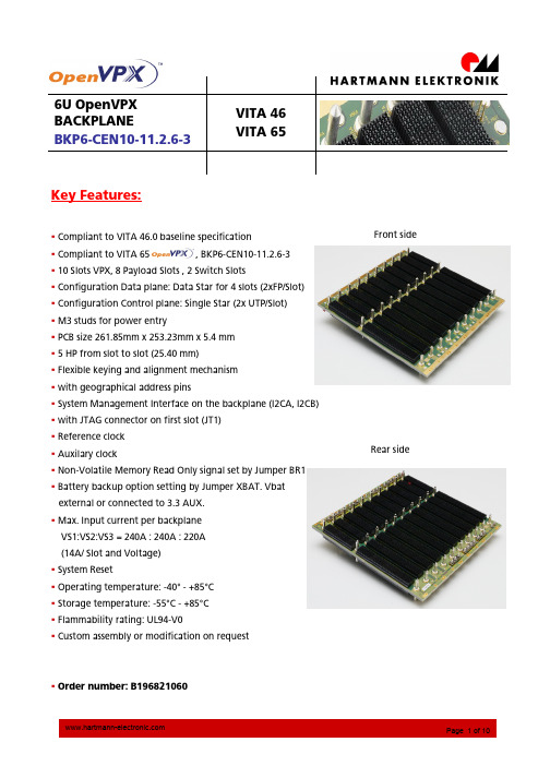
Expansion Plane Lanes of BKP6-CEN10-11.2.6-n
E P 0 1- T +
GND-J2
E P 0 1- R +
GND-J2
EP 02-T GND-J2
EP 02-R GND-J2
EP 03-T +
GND-J2
EP 03-R +
GND-J2
EP 04-T GND-J2
EP 04-R GND-J2
x4 using [7:4]
GND UD GND UD
EP 05-T GND EP 07-T GND
Expansion Plane lanes Payload slots of 10-slot backplane (DFP = 8 lanes)
EP(7:0) EP(7:0) EP(7:0) EP(7:0) EP(7:0) EP(7:0) EP(7:0) EP(7:0)
Type C Slot 1
EP(15:8)
Row C Even Row d
GND E P 0 1- R GND EP 03-R GND EP 05-R GND EP 07-R GND EP 09-R GND E P 11- R GND E P 13 - R GND E P 15 - R -
Row B Odd Row b
EP 00-R GND-J2
W25Q64中文资料精编版
W25Q64BV出版日期:2010年7月8日- 1 - 版本E64M位与串行闪存双路和四路SPIW25Q64BV- 2 -目录1,一般DESCRIPTION (5)2。
FEATURES (5)3引脚配置SOIC208-MIL.......................................... .. (6)4,焊垫配置WSON8X6-MM.......................................... . (6)5,焊垫配置PDIP300-MIL.......................................... . (7)6引脚说明SOIC208密耳,PDIP300密耳和WSON8X6-MM................................ 7......7引脚配置SOIC300mil的.......................................... .. (8)8引脚SOIC封装说明300-MIL (8)8.1包装Types (9)8.2片选(/CS) (9)8.3串行数据输入,输出和IO(DI,DO和IO0,IO1,IO2,IO3)............................. 9.......8.4写保护(/WP) (9)8.5控股(/HOLD) (9)8.6串行时钟(CLK) (9)9座DIAGRAM (10)10功能DESCRIPTION (11)10.1 SPI OPERATIONS (11)10.1.1标准SPI Instructions (11)10.1.2双SPI Instructions (11)10.1.3四路SPI Instructions (11)10.1.4保持功能 (11)10.2写保护 (12)10.2.1写保护Features (12)11,控制和状态寄存器............................................ .. (13)11.1状态REGISTER (13)11.1.1 BUSY (13)11.1.2写使能锁存(WEL) (13)11.1.3块保护位(BP2,BP1,BP0)..................................... .. (13)11.1.4顶/底块保护(TB)....................................... .................................................. ..1311.1.5部门/块保护(SEC) (13)11.1.6状态寄存器保护(SRP,SRP0)....................................... . (14)11.1.7四路启用(QE) (14)11.1.8状态寄存器内存保护........................................... .. (16)11.2 INSTRUCTIONS (17)11.2.1制造商和设备标识........................................... .. (17)11.2.2指令集表1 (18)W25Q64BV11.2.3指令表2(阅读说明书)....................................... (19)出版日期:2010年7月8日- 3 - 修订版E11.2.4写使能(06h) (20)11.2.5写禁止(04h) (20)11.2.6读状态寄存器1(05H)和读状态寄存器2(35H).............................. (21)11.2.7写状态寄存器(01H)......................................... .................................................. .. (22)11.2.8读取数据(03h) (23)11.2.9快速阅读(0Bh) (24)11.2.10快速读双输出(3BH)........................................ .................................................. 0.25 11.2.11快速读四路输出(6BH)........................................ .. (26)11.2.12快速读双I / O (BBh) (27)11.2.13快速读取四I/ O (EBh) (29)11.2.14八进制字读取四I/ O(E3H)..................................... (31)11.2.15页编程(02h) (33)11.2.16四路输入页编程(32H)........................................ . (34)11.2.17扇区擦除(20H) (35)11.2.1832KB的块擦除(52H) (36)11.2.1964KB的块擦除(D8h) (37)20年2月11日芯片擦除(C7H/ 60h) (38)21年2月11日擦除挂起(75h) (39)22年2月11日擦除恢复(7Ah) (40)23年11月2日掉电(B9h) (41)24年2月11日高性能模式(A3H)......................................... (42)25年2月11日发布掉电或高性能模式/设备ID(ABH) (42)26年2月11日读制造商/设备ID(90H)....................................... . (44)27年2月11日阅读唯一的ID号(4BH)........................................ . (45)28年2月11日读JEDEC的ID (9Fh) (46)29年2月11日连续读取模式复位(FFH或FFFFH)...................................... .. (47)12,电气特性.............................................. (48)12.1绝对最大Ratings (48)12.2操作范围 (48)12.3上电时序和写抑制阈值......................................... (49)12.4直流电气Characteristics (50)12.5 AC测量条件.............................................. .. (51)12.6 AC电气Characteristics (52)12.7 AC电气特性(续)......................................... . (53)12.8串行输出Timing (54)12.9输入Timing (54)12.10持有Timing (54)13包装SPECIFICATION (55)W25Q64BV13.18引脚SOIC208密耳(包装代号SS)..................................... .. (55)- 4 -13.28引脚PDIP300密耳(封装代码DA)..................................... (56)13.38触点WSON8x6毫米(封装代码ZE)....................................... (57)13.416引脚SOIC300密耳(封装代码SF)..................................... . (58)14订货INFORMA TION (59)14.1有效的部件号和顶端标记.......................................... (60)15版本HISTORY (61)W25Q64BV出版日期:2010年7月8日- 5 - 修订版E1概述该W25Q64BV(64M位)串行Flash存储器提供了有限的系统存储解决方案空间,引脚和电源。
PSMPS65-5中文资料

AC/DC Medical Power SupplyFEATURES Array● Medical Application● Low Cost, High Reliability● Compact Size, Light Weight● 100% Full Load Burn-In Test● Universal AC Input / Full Range● UL2601-1, EN60601-1 Approved● Built-In EMI Filter, Low Ripple Noise● High Efficiency, Low Working Temperature● Protections: Short Circuit /Overload /Over VoltageSPECIFICATIONS: PSMPS65 SeriesAll specifications are based on 25o C, Nominal Input Voltage, and Maximum Output Current unless otherwise noted.We reserve the right to change specifications based on technological advances.INPUT SPECIFICATIONSInput Voltage 90 – 264VAC (127 – 370VDC)Input Frequency 47 to 440HzAC Current (typical) 1.6A @ 115VAC / 0.9A @ 230VACInrush Current Cold start 15A @ 115VAC; 30A @ 230VACLeakage Current Less than 0.3mA @ 264VACOUTPUT SPECIFICATIONSOutput Voltage See TableVoltage Tolerance ±2.0% typicalOutput Adjustment Range ±10% rated output loadOutput Power 72W max with 18CFM minimum forced air flowLine Regulation ±1%Load Regulation ±2% typicalOutput Current See TableRipple & Noise (20MHz BW) 100mVp-p typicalSetup, Rise Time 800ms and 30ms @ 230VAC and full load / 800ms and 30ms @ 115VAC and full loadHold-Up Time 50ms @ 230VAC and full load / 16ms @ 115VAC and full load.Temperature Coefficient ±0.04%/°C (0~50°C)PROTECTIONOver Voltage Protection CH.1: 115~135% rated output voltageOverload Protection 73~105W hiccup mode, auto-recoveryGENERAL SPECIFICATIONSSwitching Frequency (fixed) 45KHzEfficiency Up to 80%Isolation Voltage (Input to Output) 4000VAC for 1 min.Isolation Voltage (Input to Field Ground) 1500VAC for 1 min.Isolation Resistance (Input to Output) 100MΩ / 500VDCENVIRONMENTAL SPECIFICATIONSOperating Temperature -10°C to +60°C (refer to derating curve)Storage Temperature -20°C to +85°COperating Humidity (non-condensing) 20% to 90% RHVibration 10~500Hz, 2G 10min./1cycle, Period for 60 minutes each along X, Y, and Z axes.MTBF 359,700 hours min. (According to MIL-HDBK-217) at 25°CPHYSICAL SPECIFICATIONSWeight 280gDimensions 127(L) x 76(W) x 42(H) mmSAFETY & EMCSafety Standards UL2601-1, TUV EN60601-1, IEC601-1 ApprovedEMC Standards EN55011 class B, EN61000-4-2,3,4,5,6,8,11, EN61000-3-2,3, EN60601-1-2, ENV50204AC/DC Medical Power SupplyOUTPUT VOLTAGE / CURRENT RATING CHARTModel Input VoltageOutput Voltage Output CurrentRange Output CurrentRipple & Noise Rated OutputPower PSMPS65-3.3 3.3 VDC 0 – 15.2A 12A 80mVp-p 39.6W PSMPS65-5 5 VDC 0 – 13.8A 12A 100mVp-p 60W PSMPS65-7.5 7.5 VDC 0 – 9.6A 8A 100mVp-p 60W PSMPS65-12 12 VDC 0 – 6A 5.2A 100mVp-p 62.4W PSMPS65-13.5 13.5 VDC 0 – 5.4A 4.7A 100mVp-p 63.5W PSMPS65-15 15 VDC 0 – 4.8A 4.2A 100mVp-p 63W PSMPS65-24 24 VDC 0 – 3A 2.7A 100mVp-p 64.8W PSMPS65-27 27 VDC 0 – 2.7A 2.4A 100mVp-p 64.8W PSMPS65-4890~264 VAC(127~370 VDC)48 VDC0 – 1.5A1.35A100mVp-p64.8WNOTES1. All parameters are specified at 230VAC input, rated load, 25°C ambient.2. Tolerances include set up tolerance, line regulation, load regulation.3. Line regulation is measured from low line to high line at rated load.4. Mounting holes M1 and M2 should be grounded for EMI purposes.5. Ripple & noise are measured at 20MHz by using a 12" twisted pair terminated with a 0.1uF & 47uF capacitor.BLOCK DIAGRAMDERATING CURVESTATIC CHARACTERISTICSAC/DC Medical Power SupplyMECHANICAL DRAWINGUnit: mmAC Input Connector (CN1): Molex 5277-02 or equivalentPin. NoAssignmentMating HousingTerminal1 AC/N2 AC/LMolex 5195or equivalent Molex 5194 or equivalentDC Output Connector (CN2): Molex 5273-06 or equivalentPin No. Assignment Mating Housing Terminal 1,2,3 +V 4,5,6 -V Molex 5195 or equivalentMolex 5194or equivalent。
EMS22P30-M25-LS6中文资料(bourns)中文数据手册「EasyDatasheet - 矽搜」

电气特性
解析度................................................................................................................................................................................................................ 1024国 绝缘电阻(500 VDC) ......................................................................................................................................................................1,000兆欧 电气行程........................................................................................................................................................................................................续 电源电压........................................................................................................................................................................5.0 VDC±10%,3.3 VDC±10% 电源电流.................................................................................................................................................................................................20 mA(最大值)
CommScope 65°高度宽度螺纹扁球型扬声器说明书

24-port sector antenna, 4x 694-960, 4x 1427-2690, 4x 1695-2180, 4x2490-2690 MHz, 65° HPBW, and 8x 3300-3800 MHz, 90° HPBW, 8xRETAntenna includes 2x Single Column X-Pol Arrays for 694-960MHz and 2x Single Column X-PolArrays for 1427-2690MHz, suitable for 4x MIMO applicationsIncludes 2x Single Column X-Pol Diplexed Arrays providing 4-Ports x 1695-2180MHz and 4 Portsx 2490-2690MHz, suitable for 4x MIMO applicationsRetractable tilt indicator rodsIncludes eight Internal RET’s. All 2490-2690MHz (Y1&Y4) ports share common RETM-LOC cluster connector for 3.3-3.8GHz, equipped with calibration portAntenna shape optimized for wind load reductionGeneral SpecificationsAntenna Type Sector- and beamformingBand MultibandCalibration Connector Interface M-LOCCalibration Connector Quantity1Color Light Gray (RAL 7035)Grounding Type RF connector inner conductor and body grounded to reflector and mountingbracketPerformance Note Outdoor usageRadome Material Fiberglass, UV resistantReflector Material AluminumRF Connector Interface 4.3-10 Female | M-LOCRF Connector Location BottomRF Connector Quantity, high band8RF Connector Quantity, mid band12RF Connector Quantity, low band4RF Connector Quantity, total24Remote Electrical Tilt (RET) InformationRET Hardware CommRET v2RET Interface8-pin DIN Female | 8-pin DIN MaleRET Interface, quantity 2 female | 2 male16Page ofPage of 26Input Voltage 10–30 VdcInternal RETHigh band (1) | Low band (2) | Mid band (5)Power Consumption, active state, maximum 8 W Power Consumption, idle state, maximum 1 WProtocol3GPP/AISG 2.0 (Single RET)DimensionsWidth 430 mm | 16.929 in Depth 197 mm | 7.756 in Length2100 mm | 82.677 in Net Weight, antenna only 41.2 kg | 90.83 lb TDD Column Spacing42 mm | 1.654 inArray LayoutPort ConfigurationElectrical SpecificationsImpedance50 ohmOperating Frequency Band1427 – 2690 MHz | 1695 – 2180 MHz | 2490 – 2690 MHz | 3300 – 3800MHz | 694 – 960 MHzPolarization±45°Total Input Power, maximum900 W @ 50 °CElectrical SpecificationsFrequency Band, MHz694–790790–890890–9601427–15181695–22002300–26901695–21802490–26903300–3800 Gain, dBi14.1151514.115.916.617.117.716706059696361696482 Beamwidth, Horizontal,degrees10.69.58.79.97.6 6.2 5.2 4.2 6.1 Beamwidth, Vertical,degreesBeam Tilt, degrees2–122–122–122–122–122–122–122–122–12USLS (First Lobe), dB201918131820192116313130343431323229Front-to-Back Ratio at 180°,dB26Coupling level, Amp,Antenna port to Cal port, dBCoupling level, max Amp ∆,±2Antenna port to Cal port, dB36Page ofCoupler, max Amp ∆,0.9Antenna port to Cal port, dB7Coupler, max Phase ∆,Antenna port to Cal port,degrees272727262626272725 Isolation, CrossPolarization, dBIsolation, Inter-band, dB272727262626262725 Isolation, Co-polarization, dB19VSWR | Return loss, dB 1.5 | 14.0 1.5 | 14.0 1.5 | 14.0 1.5 | 14.0 1.5 | 14.0 1.5 | 14.0 1.5 | 14.0 1.5 | 14.0 1.5 | 14.0-153-153-153-153-153-153-153-153-140PIM, 3rd Order, 2 x 20 W,dBc25025025020020015020015075Input Power per Port at 50°C, maximum, wattsElectrical Specifications, BASTAFrequency Band, MHz694–790790–890890–9601427–15181695–22002300–26901695–21802490–26903300–380013.614.614.613.715.316.216.617.415.3Gain by all Beam Tilts,average, dBiGain by all Beam Tilts±0.6±0.5±0.4±0.5±1±0.5±0.7±0.3±0.8 Tolerance, dB±8.3±4.6±4.7±7.3±8.4±4.1±6.4±2.5±22.1 Beamwidth, HorizontalTolerance, degreesBeamwidth, Vertical±0.7±0.7±0.4±0.7±0.9±0.5±0.4±0.2±0.6 Tolerance, degrees19.417.417.613.214.913.515.91513.2 USLS, beampeak to 20°above beampeak, dBFront-to-Back Total Power222421222826262422at 180° ± 30°, dBCPR at Boresight, dB222323161817182318 Electrical Specifications, Broadcast 65°Frequency Band, MHz3300–3800 Gain, dBi16.557 Beamwidth, Horizontal,degrees6.1 Beamwidth, Vertical,degreesFront-to-Back Total Power24at 180° ± 30°, dB1746Page ofUSLS (First Lobe), dB17 Electrical Specifications, Service BeamFrequency Band, MHz3300–3800 Steered 0° Gain, dBi20.823Steered 0° Beamwidth,Horizontal, degrees30Steered 0° Front-to-BackTotal Power at 180° ± 30°,dB15Steered 0° HorizontalSidelobe, dBSteered 30° Gain, dBi19.6 Steered 30° Beamwidth,28 Horizontal, degrees28Steered 30° Front-to-BackTotal Power at 180° ± 30°,dBElectrical Specifications, Soft SplitFrequency Band, MHz3300–3800 Gain, dBi19.7 Beamwidth, Horizontal,31degrees28Front-to-Back Total Powerat 180° ± 30°, dBHorizontal Sidelobe, dB16 Mechanical SpecificationsWind Loading @ Velocity, frontal495.0 N @ 150 km/h (111.3 lbf @ 150 km/h)Wind Loading @ Velocity, lateral253.0 N @ 150 km/h (56.9 lbf @ 150 km/h)Wind Loading @ Velocity, maximum745.0 N @ 150 km/h (167.5 lbf @ 150 km/h)Wind Loading @ Velocity, rear316.0 N @ 150 km/h (71.0 lbf @ 150 km/h)Wind Speed, maximum241 km/h (150 mph)Packaging and WeightsWidth, packed530 mm | 20.866 inDepth, packed349 mm | 13.74 in2272 mm | 89.449 in56Page ofLength, packed2272 mm | 89.449 inWeight, gross53.5 kg | 117.947 lbRegulatory Compliance/CertificationsAgency ClassificationCHINA-ROHS Below maximum concentration valueISO 9001:2015Designed, manufactured and/or distributed under this quality management system REACH-SVHC Compliant as per SVHC revision on /ProductCompliance ROHS CompliantUK-ROHSCompliant/ExemptedIncluded ProductsBSAMNT-3–Wide Profile Antenna Downtilt Mounting Kit for 2.4 - 4.5 in (60 - 115 mm) OD round members.Kit contains one scissor top bracket set and one bottom bracket set.* FootnotesPerformance Note Severe environmental conditions may degrade optimum performancePage of66。
- 1、下载文档前请自行甄别文档内容的完整性,平台不提供额外的编辑、内容补充、找答案等附加服务。
- 2、"仅部分预览"的文档,不可在线预览部分如存在完整性等问题,可反馈申请退款(可完整预览的文档不适用该条件!)。
- 3、如文档侵犯您的权益,请联系客服反馈,我们会尽快为您处理(人工客服工作时间:9:00-18:30)。
MIN.
TYPICAL
850
MAX.
30 250
UNITS
nm V mW mW/cm2 A/W A/W A/W ns pF pF nA WHz-1/2 nA/LUX
0.52
up to 7.5 0.20 0.55 0.15 3.5 15 3.5 1.0 3.3 x 10⁻¹⁴ 6
4.0 5.0
*All the parameters are characteristics of a photodiode operating at 23˚C, and connected to a load resistance of 50 ohms (where appropriate).
BPX-65 Series
ABSOLUTE MAXIMUM RATINGS
Max. Rating Storage Temperature Operating Temperature Active Element Dimensions Recommended Wavelength Range High Frequency Response Field of View (BPX-65) -55 to +100 -40 to +80 1x1 400 to 1000 up to 100 74 Unit ˚C ˚C mm nm MHz DEG BPX-65 BPX-65B BPX-65R AX65-R2F
28
ቤተ መጻሕፍቲ ባይዱ
2088 Anchor Court • Newbury Park • CA 91320-1601 805.499.5902 • Fax 805.499.7770 • Sales and Technical 1.800.700.2088
0703
High Speed Photodiodes
The BPX-65 is a high speed, high quality silicon photodetector which is manufactured in large quantity and offers an excellent price-to-performance ratio. Its high frequency response, sensitivity and low cost make the BPX-65 suitable for applications including fiber optic communications, shaft encoders, computer light pens, and laser instrumentations. The photodetector consists of a 1 mm2 active element mounted in a hermetically sealed TO-18 equivalent package. The cathode is connected to the case, although a special isolated version, the BPX-65R, is available upon request. This device is also available in a special package for fiber optic applications, the AX65-R2F; with a "bug eye" lens, the BPX-65B; or even in die form. Centro Vision Inc. can also supply the die in a special custom designed package and/or manufacture the device to MIL SPECS.
Type No.
Package 3 4 5 7
ELECTRO-OPTICAL SPECIFICATIONS*
Peak Sensitivity Operating Voltage Power Dissipation (at 25˚C) Response Linearity (to better than 1%) Responsivity at 450nm at 900nm at 1064nm Risetime (measured at 820nm)(Vr=20V) Capacitance (Vr=0V) Capacitance (Vr=20V) Dark Current (Vr=20V) Nep at 900nm (Vr=20V) Photosensitivity (at color temp of 2856˚K) (Vr=20V) BPX-65 and Bpx-65R)