54LS00中文资料
54LS47 74LS47 中文数据手册Data Sheet
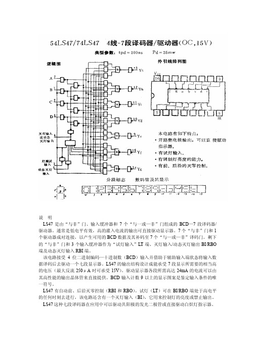
4. 当灭灯输入/脉动灭灯输出(BI/RBO)开路或保持“高”,且将“低”加到试灯输入时,所有段的输
出都得打开。
●BI/RBO 是用作灭灯输入(BI)与/或脉动灭灯输出(RBO)的线与逻辑。
符号
参数名称
规范表
Vcc 电源电压
54
74
VO(off) 关态输出电压
IO(on) 开态输出电流
54 74
IOH 输出高电平电流
BI/RBO 等效电路见附图 10;除 BI/RBO 外,其他输入的等效电路见附图 1。LT 和 RBI:Req=20kΩ, A、B、 C 和 D:Req=25kΩ a~g 典型输出线路见附图 17。 注:测ICC时,所有的输出端开路,输入端接 4.5V。、
BDTIC Semiconductor
/Semiconductor
LS47 有自动前、后沿灭零控制(RBI 和 RBO)。试灯(LT)可在 BI/RBO 端处于高电平 的任何时刻去进行,该电路还含有一个灭灯输入(BI),它用来控制灯的亮度或禁止输出。
LS47 这种七段译码器在应用中可以驱动共阳极的发光二极管或直接驱动白炽灯指示器。
功能表
十进制 或功能
输 LT RBI
入
BT/RBO
输
出
注
DCBA
●
a
b
c
d
e
fg
0
H
H
LLLL
H
开 开 开 开 开 开关
1
H
x
LLLH
H
关 开 开 关 关 关关
2
H
x
LLHL
H
开 开 关 开 开 关开
3
H
x
LLHH
汽车尾灯控制电路的几个芯片资料
‘00 最小 最大
Iik=-8mA
40
50
50
uA 20
IIL输入低电平电 流
Vcc=最大
VIL=0.4V VIL=0.5V
-1.6
-2
-0.4
-2
mA
IOS输出短路电 流
Vcc=最大
54 -20 -55 -40 -100 -40 -100 -20 -100
74
-18
-55
-40 -100 -40 -100 -20 -100 mA
ICCH输出高电平时电源电流 Vcc=最大
Vcc=最大
VIH=2.4V VIH=2.7V VIL=0.4V VIL=0.5V
54 74
40
-1.6
-20 -55 -18 -55
. ICCH输出高电平时电源电流
Vcc=最大
12
w ICCL输出低电平时电源电流
Vcc=最大
33
‘H04 最小 最大
-1.5
2.4 2.4
0.4 0.4 1
50
-2
-40 -100 -40 -100
电子器件采购平台: IC资料查询网站: 电子工程技术论坛:/bbs
电子器件采购平台: IC资料查询网站: 电子工程技术论坛:/bbs
Iik=-8mA Iik=-12mA
-1.5
Iik=-18mA
b VOH输出高电平 Vcc=最小VIL= 54
2.4
电压
最大 IOH=最大
74
2.4
b VOL输出低电平
Vcc=最大,
54
0.4
s 电压
VIH=2V,IOL=最大 74
0.4
‘H20 最小 最大
SN54LV00A中文资料

PACKAGING INFORMATIONOrderable Device Status(1)PackageType PackageDrawingPins PackageQtyEco Plan(2)Lead/Ball Finish MSL Peak Temp(3)SN74LV00AD ACTIVE SOIC D1450Green(RoHS&no Sb/Br)CU NIPDAU Level-1-260C-UNLIMSN74LV00ADBLE OBSOLETE SSOP DB14TBD Call TI Call TISN74LV00ADBR ACTIVE SSOP DB142000Green(RoHS&no Sb/Br)CU NIPDAU Level-1-260C-UNLIMSN74LV00ADBRG4ACTIVE SSOP DB142000Green(RoHS&no Sb/Br)CU NIPDAU Level-1-260C-UNLIMSN74LV00ADE4ACTIVE SOIC D1450Green(RoHS&no Sb/Br)CU NIPDAU Level-1-260C-UNLIMSN74LV00ADGVR ACTIVE TVSOP DGV142000Green(RoHS&no Sb/Br)CU NIPDAU Level-1-260C-UNLIMSN74LV00ADGVRE4ACTIVE TVSOP DGV142000Green(RoHS&no Sb/Br)CU NIPDAU Level-1-260C-UNLIMSN74LV00ADR ACTIVE SOIC D142500Green(RoHS&no Sb/Br)CU NIPDAU Level-1-260C-UNLIMSN74LV00ADRE4ACTIVE SOIC D142500Green(RoHS&no Sb/Br)CU NIPDAU Level-1-260C-UNLIMSN74LV00ANSR ACTIVE SO NS142000Green(RoHS&no Sb/Br)CU NIPDAU Level-1-260C-UNLIMSN74LV00ANSRG4ACTIVE SO NS142000Green(RoHS&no Sb/Br)CU NIPDAU Level-1-260C-UNLIMSN74LV00APW ACTIVE TSSOP PW1490Green(RoHS&no Sb/Br)CU NIPDAU Level-1-260C-UNLIMSN74LV00APWE4ACTIVE TSSOP PW1490Green(RoHS&no Sb/Br)CU NIPDAU Level-1-260C-UNLIMSN74LV00APWG4ACTIVE TSSOP PW1490Green(RoHS&no Sb/Br)CU NIPDAU Level-1-260C-UNLIM SN74LV00APWLE OBSOLETE TSSOP PW14TBD Call TI Call TISN74LV00APWR ACTIVE TSSOP PW142000Green(RoHS&no Sb/Br)CU NIPDAU Level-1-260C-UNLIMSN74LV00APWRE4ACTIVE TSSOP PW142000Green(RoHS&no Sb/Br)CU NIPDAU Level-1-260C-UNLIMSN74LV00APWRG4ACTIVE TSSOP PW142000Green(RoHS&no Sb/Br)CU NIPDAU Level-1-260C-UNLIMSN74LV00APWT ACTIVE TSSOP PW14250Green(RoHS&no Sb/Br)CU NIPDAU Level-1-260C-UNLIMSN74LV00APWTG4ACTIVE TSSOP PW14250Green(RoHS&no Sb/Br)CU NIPDAU Level-1-260C-UNLIMSN74LV00ARGYR ACTIVE QFN RGY141000Green(RoHS&no Sb/Br)CU NIPDAU Level-2-260C-1YEAR(1)The marketing status values are defined as follows:ACTIVE:Product device recommended for new designs.LIFEBUY:TI has announced that the device will be discontinued,and a lifetime-buy period is in effect.NRND:Not recommended for new designs.Device is in production to support existing customers,but TI does not recommend using this part in a new design.PREVIEW:Device has been announced but is not in production.Samples may or may not be available.OBSOLETE:TI has discontinued the production of the device.(2)Eco Plan-The planned eco-friendly classification:Pb-Free(RoHS)or Green(RoHS&no Sb/Br)-please check /productcontent for the latest availability information and additional product content details.TBD:The Pb-Free/Green conversion plan has not been defined.Pb-Free(RoHS):TI's terms"Lead-Free"or"Pb-Free"mean semiconductor products that are compatible with the current RoHS requirements for all6substances,including the requirement that lead not exceed0.1%by weight in homogeneous materials.Where designed to be soldered at high temperatures,TI Pb-Free products are suitable for use in specified lead-free processes.Green(RoHS&no Sb/Br):TI defines"Green"to mean Pb-Free(RoHS compatible),and free of Bromine(Br)and Antimony(Sb)based flame retardants(Br or Sb do not exceed0.1%by weight in homogeneous material)(3)MSL,Peak Temp.--The Moisture Sensitivity Level rating according to the JEDEC industry standard classifications,and peak solder temperature.Important Information and Disclaimer:The information provided on this page represents TI's knowledge and belief as of the date that it is provided.TI bases its knowledge and belief on information provided by third parties,and makes no representation or warranty as to the accuracy of such information.Efforts are underway to better integrate information from third parties.TI has taken and continues to take reasonable steps to provide representative and accurate information but may not have conducted destructive testing or chemical analysis on incoming materials and chemicals.TI and TI suppliers consider certain information to be proprietary,and thus CAS numbers and other limited information may not be available for release.In no event shall TI's liability arising out of such information exceed the total purchase price of the TI part(s)at issue in this document sold by TI to Customer on an annual basis.元器件交易网IMPORTANT NOTICETexas Instruments Incorporated and its subsidiaries (TI) reserve the right to make corrections, modifications,enhancements, improvements, and other changes to its products and services at any time and to discontinueany product or service without notice. Customers should obtain the latest relevant information before placingorders and should verify that such information is current and complete. All products are sold subject to TI’s termsand conditions of sale supplied at the time of order acknowledgment.TI warrants performance of its hardware products to the specifications applicable at the time of sale inaccordance with TI’s standard warranty. T esting and other quality control techniques are used to the extent TIdeems necessary to support this warranty. Except where mandated by government requirements, testing of allparameters of each product is not necessarily performed.TI assumes no liability for applications assistance or customer product design. Customers are responsible fortheir products and applications using TI components. T o minimize the risks associated with customer productsand applications, customers should provide adequate design and operating safeguards.TI does not warrant or represent that any license, either express or implied, is granted under any TI patent right,copyright, mask work right, or other TI intellectual property right relating to any combination, machine, or processin which TI products or services are used. Information published by TI regarding third-party products or servicesdoes not constitute a license from TI to use such products or services or a warranty or endorsement thereof.Use of such information may require a license from a third party under the patents or other intellectual propertyof the third party, or a license from TI under the patents or other intellectual property of TI.Reproduction of information in TI data books or data sheets is permissible only if reproduction is withoutalteration and is accompanied by all associated warranties, conditions, limitations, and notices. Reproductionof this information with alteration is an unfair and deceptive business practice. TI is not responsible or liable forsuch altered documentation.Resale of TI products or services with statements different from or beyond the parameters stated by TI for thatproduct or service voids all express and any implied warranties for the associated TI product or service andis an unfair and deceptive business practice. TI is not responsible or liable for any such statements.Following are URLs where you can obtain information on other Texas Instruments products and applicationsolutions:Products ApplicationsAmplifiers Audio /audioData Converters Automotive /automotiveDSP Broadband /broadbandInterface Digital Control /digitalcontrolLogic Military /militaryPower Mgmt Optical Networking /opticalnetworkMicrocontrollers Security /securityTelephony /telephonyVideo & Imaging /videoWireless /wirelessMailing Address:Texas InstrumentsPost Office Box 655303 Dallas, Texas 75265Copyright 2005, Texas Instruments Incorporated。
SN54LS123中文资料

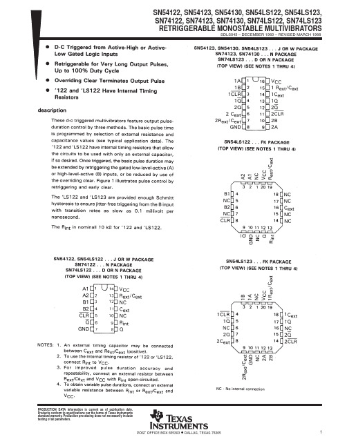
RETRIGGERABLE MONOSTABLE MULTIVIBRATORSThese dc triggered multivibrators feature pulse width control by three meth-ods. The basic pulse width is programmed by selection of external resistance and capacitance values. The LS122 has an internal timing resistor that allows the circuits to be used with only an external capacitor. Once triggered, the ba-sic pulse width may be extended by retriggering the gated low-level-active (A)or high-level-active (B) inputs, or be reduced by use of the overriding clear.•Overriding Clear Terminates Output Pulse•Compensated for V CC and T emperature Variations•DC Triggered from Active-High or Active-Low Gated Logic Inputs •Retriggerable for Very Long Output Pulses, up to 100% Duty Cycle •Internal Timing Resistors on LS122SN54/74LS122 (TOP VIEW)(SEE NOTES 1 THRU 4)SN54/74LS123 (TOP VIEW)(SEE NOTES 1 THRU 4)NOTES:1.An external timing capacitor may be connected between C ext and R ext /C ext (positive).2.To use the internal timing resistor of the LS122, connect R int to V CC .3.For improved pulse width accuracy connect an external resistor between R ext /C ext and V CC with R int open-circuited.4.To obtain variable pulse widths, connect an external variable resistance between R int /C ext and V CC .R ext/CR ext/C ext 11ĂRext/2CLRC extNC Ċ NO INTERNAL CONNECTION.。
54ls00芯片手册

54ls00芯片手册【最新版】目录1.54ls00 芯片概述2.54ls00 芯片的主要特性3.54ls00 芯片的引脚功能4.54ls00 芯片的内部结构5.54ls00 芯片的工作原理6.54ls00 芯片的应用实例正文一、54ls00 芯片概述54ls00 是一款 4 位同步十进制计数器,具有多种输入输出方式,可以实现多种计数功能。
该芯片主要应用于数字电路、计算机硬件、通信设备等领域。
二、54ls00 芯片的主要特性1.电源电压范围:54ls00 芯片的工作电压范围为 3V 至 30V,适应性强。
2.时钟输入:芯片有多种时钟输入方式,如 CP(时钟输入)、CLK(时钟锁存输入)等。
3.计数模式:54ls00 支持四种计数模式,分别为二进制、BCD、十进制和异步清零。
4.输出方式:芯片具有多种输出方式,如并行输出、串行输出和异步清零输出等。
三、54ls00 芯片的引脚功能1.CP(时钟输入):输入时钟信号,用于控制计数器的计数。
2.CLK(时钟锁存输入):输入时钟信号,用于锁存计数值。
3.EN(使能):控制计数器的启动和停止。
4.BCD OUT(BCD 输出):输出计数值的 BCD 编码。
5.PAR(并行输出):输出计数值的并行信号。
6.SISO(串行输出):输出计数值的串行信号。
7.OE(输出使能):控制输出信号的使能。
8.MR(异步清零):输入异步清零信号,用于清零计数值。
9.VCC(电源正极):连接电源正极。
10.GND(电源负极):连接电源负极。
四、54ls00 芯片的内部结构54ls00 芯片内部包含一个 4 位计数器、一个寄存器、一个译码器和多个逻辑门。
计数器用于计数输入时钟信号,寄存器用于存储计数值,译码器用于将计数值转换为 BCD 编码,逻辑门用于实现各种输入输出功能。
五、54ls00 芯片的工作原理1.当 CP(时钟输入)和 CLK(时钟锁存输入)同时为高电平时,计数器计数并锁存当前值。
SN54LS123J中文资料
PRODUCTION DATA information is current as of publication date.Products conform to specifications per the terms of Texas Instrumentsstandard warranty. Production processing does not necessarily includetesting of all parameters.1POST OFFICE BOX 655303 • DALLAS, TEXAS 752652POST OFFICE BOX 655303 • DALLAS, TEXAS 752653 POST OFFICE BOX 655303 • DALLAS, TEXAS 752654POST OFFICE BOX 655303 • DALLAS, TEXAS 752655 POST OFFICE BOX 655303 • DALLAS, TEXAS 752656POST OFFICE BOX 655303 • DALLAS, TEXAS 752657 POST OFFICE BOX 655303 • DALLAS, TEXAS 752658POST OFFICE BOX 655303 • DALLAS, TEXAS 752659 POST OFFICE BOX 655303 • DALLAS, TEXAS 75265PACKAGING INFORMATIONOrderable Device Status (1)Package Type Package DrawingPins Package Qty Eco Plan (2)Lead/Ball FinishMSL Peak Temp (3)5962-7603901VEA ACTIVE CDIP J 161None Call TI Level-NC-NC-NC 5962-7603901VFAACTIVE CFP W 161None Call TI Level-NC-NC-NC 7603901EA ACTIVE CDIP J 161None Call TI Level-NC-NC-NC 7603901FA ACTIVE CFP W 161None Call TI Level-NC-NC-NC JM38510/01203BEA ACTIVE CDIP J 161None Call TI Level-NC-NC-NC JM38510/31401B2A ACTIVE LCCC FK 201None Call TI Level-NC-NC-NC JM38510/31401BEA ACTIVE CDIP J 161None Call TI Level-NC-NC-NC JM38510/31401BFAACTIVE CFP W 161None Call TI Level-NC-NC-NC SN54122J OBSOLETE CDIP J 14None Call TI Call TISN54123J ACTIVE CDIP J 161None Call TI Level-NC-NC-NC SN54LS123J ACTIVE CDIP J 161None Call TI Level-NC-NC-NC SN74122N OBSOLETE PDIP N 14None Call TI Call TISN74123N ACTIVE PDIP N 1625Pb-Free (RoHS)CU NIPDAU Level-NC-NC-NC SN74123N3OBSOLETE PDIP N 16None Call TI Call TISN74LS122D ACTIVE SOIC D 1450Pb-Free (RoHS)CU NIPDAU Level-2-260C-1YEAR/Level-1-235C-UNLIM SN74LS122DR ACTIVE SOIC D 142500Pb-Free (RoHS)CU NIPDAU Level-2-260C-1YEAR/Level-1-235C-UNLIM SN74LS122N ACTIVE PDIP N 1425Pb-Free (RoHS)CU NIPDAU Level-NC-NC-NC SN74LS122N3OBSOLETE PDIP N 14None Call TI Call TISN74LS122NSR ACTIVE SO NS 142000Pb-Free (RoHS)CU NIPDAU Level-2-260C-1YEAR/Level-1-235C-UNLIM SN74LS123D ACTIVE SOIC D 1640Pb-Free (RoHS)CU NIPDAU Level-2-260C-1YEAR/Level-1-235C-UNLIM SN74LS123DR ACTIVE SOIC D 162500Pb-Free (RoHS)CU NIPDAU Level-2-260C-1YEAR/Level-1-235C-UNLIM SN74LS123J OBSOLETE CDIP J 16None Call TI Call TISN74LS123N ACTIVE PDIP N 1625Pb-Free (RoHS)CU NIPDAU Level-NC-NC-NC SN74LS123N3OBSOLETE PDIP N 16None Call TI Call TISN74LS123NSR ACTIVE SO NS 162000Pb-Free (RoHS)CU NIPDAU Level-2-260C-1YEAR/Level-1-235C-UNLIM SNJ54122J OBSOLETE CDIP J 14None Call TI Call TISNJ54123J ACTIVE CDIP J 161None Call TI Level-NC-NC-NC SNJ54123W ACTIVE CFP W 161None Call TI Level-NC-NC-NC SNJ54LS123FK ACTIVE LCCC FK 201None Call TI Level-NC-NC-NC SNJ54LS123J ACTIVE CDIP J 161None Call TI Level-NC-NC-NC SNJ54LS123WACTIVECFPW161NoneCall TILevel-NC-NC-NC(1)The marketing status values are defined as follows:ACTIVE:Product device recommended for new designs.LIFEBUY:TI has announced that the device will be discontinued,and a lifetime-buy period is in effect.NRND:Not recommended for new designs.Device is in production to support existing customers,but TI does not recommend using this part in a new design.PREVIEW:Device has been announced but is not in production.Samples may or may not be available.PACKAGE OPTION ADDENDUM28-Feb-2005Addendum-Page 1元器件交易网OBSOLETE:TI has discontinued the production of the device.(2)Eco Plan -May not be currently available -please check /productcontent for the latest availability information and additional product content details.None:Not yet available Lead (Pb-Free).Pb-Free (RoHS):TI's terms "Lead-Free"or "Pb-Free"mean semiconductor products that are compatible with the current RoHS requirements for all 6substances,including the requirement that lead not exceed 0.1%by weight in homogeneous materials.Where designed to be soldered at high temperatures,TI Pb-Free products are suitable for use in specified lead-free processes.Green (RoHS &no Sb/Br):TI defines "Green"to mean "Pb-Free"and in addition,uses package materials that do not contain halogens,including bromine (Br)or antimony (Sb)above 0.1%of total product weight.(3)MSL,Peak Temp.--The Moisture Sensitivity Level rating according to the JEDECindustry standard classifications,and peak solder temperature.Important Information and Disclaimer:The information provided on this page represents TI's knowledge and belief as of the date that it is provided.TI bases its knowledge and belief on information provided by third parties,and makes no representation or warranty as to the accuracy of such information.Efforts are underway to better integrate information from third parties.TI has taken and continues to take reasonable steps to provide representative and accurate information but may not have conducted destructive testing or chemical analysis on incoming materials and chemicals.TI and TI suppliers consider certain information to be proprietary,and thus CAS numbers and other limited information may not be available for release.In no event shall TI's liability arising out of such information exceed the total purchase price of the TI part(s)at issue in this document sold by TI to Customer on an annualbasis.PACKAGE OPTION ADDENDUM 28-Feb-2005Addendum-Page 2IMPORTANT NOTICETexas Instruments Incorporated and its subsidiaries (TI) reserve the right to make corrections, modifications, enhancements, improvements, and other changes to its products and services at any time and to discontinue any product or service without notice. Customers should obtain the latest relevant information before placing orders and should verify that such information is current and complete. All products are sold subject to TI’s terms and conditions of sale supplied at the time of order acknowledgment.TI warrants performance of its hardware products to the specifications applicable at the time of sale in accordance with TI’s standard warranty. T esting and other quality control techniques are used to the extent TI deems necessary to support this warranty. Except where mandated by government requirements, testing of all parameters of each product is not necessarily performed.TI assumes no liability for applications assistance or customer product design. Customers are responsible for their products and applications using TI components. T o minimize the risks associated with customer products and applications, customers should provide adequate design and operating safeguards.TI does not warrant or represent that any license, either express or implied, is granted under any TI patent right, copyright, mask work right, or other TI intellectual property right relating to any combination, machine, or process in which TI products or services are used. Information published by TI regarding third-party products or services does not constitute a license from TI to use such products or services or a warranty or endorsement thereof. Use of such information may require a license from a third party under the patents or other intellectual property of the third party, or a license from TI under the patents or other intellectual property of TI.Reproduction of information in TI data books or data sheets is permissible only if reproduction is without alteration and is accompanied by all associated warranties, conditions, limitations, and notices. Reproduction of this information with alteration is an unfair and deceptive business practice. TI is not responsible or liable for such altered documentation.Resale of TI products or services with statements different from or beyond the parameters stated by TI for that product or service voids all express and any implied warranties for the associated TI product or service and is an unfair and deceptive business practice. TI is not responsible or liable for any such statements. Following are URLs where you can obtain information on other Texas Instruments products and application solutions:Products ApplicationsAmplifiers Audio /audioData Converters Automotive /automotiveDSP Broadband /broadbandInterface Digital Control /digitalcontrolLogic Military /militaryPower Mgmt Optical Networking /opticalnetwork Microcontrollers Security /securityTelephony /telephonyVideo & Imaging /videoWireless /wirelessMailing Address:Texas InstrumentsPost Office Box 655303 Dallas, Texas 75265Copyright 2005, Texas Instruments Incorporated。
SNJ54LS02FK中文资料
PACKAGING INFORMATIONOrderable Device Status(1)PackageType PackageDrawingPins PackageQtyEco Plan(2)Lead/Ball Finish MSL Peak Temp(3)JM38510/00401BCA ACTIVE CDIP J141TBD Call TI Level-NC-NC-NCJM38510/00401BDA ACTIVE CFP W141TBD Call TI Level-NC-NC-NCJM38510/00401BDA ACTIVE CFP W141TBD Call TI Level-NC-NC-NCJM38510/07301BCA ACTIVE CDIP J141TBD Call TI Level-NC-NC-NCJM38510/07301BCA ACTIVE CDIP J141TBD Call TI Level-NC-NC-NCJM38510/07301BDA ACTIVE CFP W141TBD Call TI Level-NC-NC-NCJM38510/07301BDA ACTIVE CFP W141TBD Call TI Level-NC-NC-NCJM38510/30301B2A ACTIVE LCCC FK201TBD Call TI Level-NC-NC-NCJM38510/30301B2A ACTIVE LCCC FK201TBD Call TI Level-NC-NC-NCJM38510/30301BCA ACTIVE CDIP J141TBD Call TI Level-NC-NC-NCJM38510/30301BCA ACTIVE CDIP J141TBD Call TI Level-NC-NC-NCJM38510/30301BDA ACTIVE CFP W141TBD Call TI Level-NC-NC-NCJM38510/30301BDA ACTIVE CFP W141TBD Call TI Level-NC-NC-NCJM38510/30301SCA ACTIVE CDIP J141TBD Call TI Level-NC-NC-NCJM38510/30301SCA ACTIVE CDIP J141TBD Call TI Level-NC-NC-NCJM38510/30301SDA ACTIVE CFP W141TBD Call TI Level-NC-NC-NCJM38510/30301SDA ACTIVE CFP W141TBD Call TI Level-NC-NC-NC SN5402J ACTIVE CDIP J141TBD Call TI Level-NC-NC-NC SN5402J ACTIVE CDIP J141TBD Call TI Level-NC-NC-NC SN54LS02J ACTIVE CDIP J141TBD Call TI Level-NC-NC-NC SN54LS02J ACTIVE CDIP J141TBD Call TI Level-NC-NC-NC SN54S02J ACTIVE CDIP J141TBD Call TI Level-NC-NC-NC SN54S02J ACTIVE CDIP J141TBD Call TI Level-NC-NC-NC SN7402N ACTIVE PDIP N1425Pb-Free(RoHS)CU NIPDAU Level-NC-NC-NCSN7402N ACTIVE PDIP N1425Pb-Free(RoHS)CU NIPDAU Level-NC-NC-NC SN7402N3OBSOLETE PDIP N14TBD Call TI Call TISN7402N3OBSOLETE PDIP N14TBD Call TI Call TISN7402NE4ACTIVE PDIP N1425Pb-Free(RoHS)CU NIPDAU Level-NC-NC-NCSN7402NE4ACTIVE PDIP N1425Pb-Free(RoHS)CU NIPDAU Level-NC-NC-NCSN74LS02D ACTIVE SOIC D1450Green(RoHS&no Sb/Br)CU NIPDAU Level-1-260C-UNLIMSN74LS02D ACTIVE SOIC D1450Green(RoHS&no Sb/Br)CU NIPDAU Level-1-260C-UNLIMSN74LS02DE4ACTIVE SOIC D1450Green(RoHS&no Sb/Br)CU NIPDAU Level-1-260C-UNLIMSN74LS02DE4ACTIVE SOIC D1450Green(RoHS&no Sb/Br)CU NIPDAU Level-1-260C-UNLIMSN74LS02DR ACTIVE SOIC D142500Green(RoHS&no Sb/Br)CU NIPDAU Level-1-260C-UNLIMSN74LS02DR ACTIVE SOIC D142500Green(RoHS&no Sb/Br)CU NIPDAU Level-1-260C-UNLIMOrderable Device Status(1)PackageType PackageDrawingPins PackageQtyEco Plan(2)Lead/Ball Finish MSL Peak Temp(3)SN74LS02DRE4ACTIVE SOIC D142500Green(RoHS&no Sb/Br)CU NIPDAU Level-1-260C-UNLIMSN74LS02DRE4ACTIVE SOIC D142500Green(RoHS&no Sb/Br)CU NIPDAU Level-1-260C-UNLIM SN74LS02J OBSOLETE CDIP J14TBD Call TI Call TISN74LS02J OBSOLETE CDIP J14TBD Call TI Call TISN74LS02N ACTIVE PDIP N1425Pb-Free(RoHS)CU NIPDAU Level-NC-NC-NCSN74LS02N ACTIVE PDIP N1425Pb-Free(RoHS)CU NIPDAU Level-NC-NC-NC SN74LS02N3OBSOLETE PDIP N14TBD Call TI Call TISN74LS02N3OBSOLETE PDIP N14TBD Call TI Call TISN74LS02NE4ACTIVE PDIP N1425Pb-Free(RoHS)CU NIPDAU Level-NC-NC-NCSN74LS02NE4ACTIVE PDIP N1425Pb-Free(RoHS)CU NIPDAU Level-NC-NC-NCSN74LS02NSR ACTIVE SO NS142000Green(RoHS&no Sb/Br)CU NIPDAU Level-1-260C-UNLIMSN74LS02NSR ACTIVE SO NS142000Green(RoHS&no Sb/Br)CU NIPDAU Level-1-260C-UNLIMSN74LS02NSRG4ACTIVE SO NS142000Green(RoHS&no Sb/Br)CU NIPDAU Level-1-260C-UNLIMSN74LS02NSRG4ACTIVE SO NS142000Green(RoHS&no Sb/Br)CU NIPDAU Level-1-260C-UNLIMSN74S02D ACTIVE SOIC D1450Green(RoHS&no Sb/Br)CU NIPDAU Level-1-260C-UNLIMSN74S02D ACTIVE SOIC D1450Green(RoHS&no Sb/Br)CU NIPDAU Level-1-260C-UNLIMSN74S02DE4ACTIVE SOIC D1450Green(RoHS&no Sb/Br)CU NIPDAU Level-1-260C-UNLIMSN74S02DE4ACTIVE SOIC D1450Green(RoHS&no Sb/Br)CU NIPDAU Level-1-260C-UNLIM SN74S02DR OBSOLETE SOIC D14TBD Call TI Call TISN74S02DR OBSOLETE SOIC D14TBD Call TI Call TISN74S02N ACTIVE PDIP N1425Pb-Free(RoHS)CU NIPDAU Level-NC-NC-NCSN74S02N ACTIVE PDIP N1425Pb-Free(RoHS)CU NIPDAU Level-NC-NC-NC SN74S02N3OBSOLETE PDIP N14TBD Call TI Call TISN74S02N3OBSOLETE PDIP N14TBD Call TI Call TISN74S02NE4ACTIVE PDIP N1425Pb-Free(RoHS)CU NIPDAU Level-NC-NC-NCSN74S02NE4ACTIVE PDIP N1425Pb-Free(RoHS)CU NIPDAU Level-NC-NC-NC SNJ5402J ACTIVE CDIP J141TBD Call TI Level-NC-NC-NC SNJ5402J ACTIVE CDIP J141TBD Call TI Level-NC-NC-NC SNJ5402W ACTIVE CFP W141TBD Call TI Level-NC-NC-NC SNJ5402W ACTIVE CFP W141TBD Call TI Level-NC-NC-NC SNJ54LS02FK ACTIVE LCCC FK201TBD Call TI Level-NC-NC-NCOrderable Device Status(1)PackageType PackageDrawingPins PackageQtyEco Plan(2)Lead/Ball Finish MSL Peak Temp(3)SNJ54LS02FK ACTIVE LCCC FK201TBD Call TI Level-NC-NC-NC SNJ54LS02J ACTIVE CDIP J141TBD Call TI Level-NC-NC-NC SNJ54LS02J ACTIVE CDIP J141TBD Call TI Level-NC-NC-NC SNJ54LS02W ACTIVE CFP W141TBD Call TI Level-NC-NC-NC SNJ54LS02W ACTIVE CFP W141TBD Call TI Level-NC-NC-NC SNJ54S02FK ACTIVE LCCC FK201TBD Call TI Level-NC-NC-NC SNJ54S02FK ACTIVE LCCC FK201TBD Call TI Level-NC-NC-NCSNJ54S02J ACTIVE CDIP J141TBD Call TI Level-NC-NC-NCSNJ54S02J ACTIVE CDIP J141TBD Call TI Level-NC-NC-NCSNJ54S02W ACTIVE CFP W141TBD Call TI Level-NC-NC-NCSNJ54S02W ACTIVE CFP W141TBD Call TI Level-NC-NC-NC(1)The marketing status values are defined as follows:ACTIVE:Product device recommended for new designs.LIFEBUY:TI has announced that the device will be discontinued,and a lifetime-buy period is in effect.NRND:Not recommended for new designs.Device is in production to support existing customers,but TI does not recommend using this part in a new design.PREVIEW:Device has been announced but is not in production.Samples may or may not be available.OBSOLETE:TI has discontinued the production of the device.(2)Eco Plan-The planned eco-friendly classification:Pb-Free(RoHS)or Green(RoHS&no Sb/Br)-please check /productcontent for the latest availability information and additional product content details.TBD:The Pb-Free/Green conversion plan has not been defined.Pb-Free(RoHS):TI's terms"Lead-Free"or"Pb-Free"mean semiconductor products that are compatible with the current RoHS requirements for all6substances,including the requirement that lead not exceed0.1%by weight in homogeneous materials.Where designed to be soldered at high temperatures,TI Pb-Free products are suitable for use in specified lead-free processes.Green(RoHS&no Sb/Br):TI defines"Green"to mean Pb-Free(RoHS compatible),and free of Bromine(Br)and Antimony(Sb)based flame retardants(Br or Sb do not exceed0.1%by weight in homogeneous material)(3)MSL,Peak Temp.--The Moisture Sensitivity Level rating according to the JEDEC industry standard classifications,and peak solder temperature.Important Information and Disclaimer:The information provided on this page represents TI's knowledge and belief as of the date that it is provided.TI bases its knowledge and belief on information provided by third parties,and makes no representation or warranty as to the accuracy of such information.Efforts are underway to better integrate information from third parties.TI has taken and continues to take reasonable steps to provide representative and accurate information but may not have conducted destructive testing or chemical analysis on incoming materials and chemicals.TI and TI suppliers consider certain information to be proprietary,and thus CAS numbers and other limited information may not be available for release.In no event shall TI's liability arising out of such information exceed the total purchase price of the TI part(s)at issue in this document sold by TI to Customer on an annual basis.元器件交易网IMPORTANT NOTICETexas Instruments Incorporated and its subsidiaries (TI) reserve the right to make corrections, modifications, enhancements, improvements, and other changes to its products and services at any time and to discontinue any product or service without notice. Customers should obtain the latest relevant information before placing orders and should verify that such information is current and complete. All products are sold subject to TI’s terms and conditions of sale supplied at the time of order acknowledgment.TI warrants performance of its hardware products to the specifications applicable at the time of sale in accordance with TI’s standard warranty. T esting and other quality control techniques are used to the extent TI deems necessary to support this warranty. Except where mandated by government requirements, testing of all parameters of each product is not necessarily performed.TI assumes no liability for applications assistance or customer product design. Customers are responsible for their products and applications using TI components. T o minimize the risks associated with customer products and applications, customers should provide adequate design and operating safeguards.TI does not warrant or represent that any license, either express or implied, is granted under any TI patent right, copyright, mask work right, or other TI intellectual property right relating to any combination, machine, or process in which TI products or services are used. Information published by TI regarding third-party products or services does not constitute a license from TI to use such products or services or a warranty or endorsement thereof. Use of such information may require a license from a third party under the patents or other intellectual property of the third party, or a license from TI under the patents or other intellectual property of TI.Reproduction of information in TI data books or data sheets is permissible only if reproduction is without alteration and is accompanied by all associated warranties, conditions, limitations, and notices. Reproduction of this information with alteration is an unfair and deceptive business practice. TI is not responsible or liable for such altered documentation.Resale of TI products or services with statements different from or beyond the parameters stated by TI for that product or service voids all express and any implied warranties for the associated TI product or service and is an unfair and deceptive business practice. TI is not responsible or liable for any such statements. Following are URLs where you can obtain information on other Texas Instruments products and application solutions:Products ApplicationsAmplifiers Audio /audioData Converters Automotive /automotiveDSP Broadband /broadbandInterface Digital Control /digitalcontrolLogic Military /militaryPower Mgmt Optical Networking /opticalnetwork Microcontrollers Security /securityTelephony /telephonyVideo & Imaging /videoWireless /wirelessMailing Address:Texas InstrumentsPost Office Box 655303 Dallas, Texas 75265Copyright 2005, Texas Instruments Incorporated。
SN54LS07_91中文资料

元器件交易网SN54LS07, SN74LS07, SN74LS17HEX BUFFERS/DRIVERS WITHOPEN-COLLECTOR HIGH-VOLTAGE OUTPUTSCopyright 1991, Texas Instruments IncorporatedV OH High-level output voltage V SN54LS07SN54LS07, SN74LS07, SN74LS17HEX BUFFERS/DRIVERS WITH OPEN-COLLECTOR HIGH-VOLTAGE OUTPUTS元器件交易网I OHV OL V CC = MIN,V IL = 0.8 V V CC = MIN,V IH = 2 V V mA SN54LS07PARAMETERTEST CONDITIONS MIN TYP MAX UNIT A Y R L = 110 Ω,C L = 15 pF nsSN54LS07, SN74LS07, SN74LS17HEX BUFFERS/DRIVERS WITH OPEN-COLLECTOR HIGH-VOLTAGE OUTPUTS元器件交易网元器件交易网IMPORTANT NOTICETexas Instruments (TI) reserves the right to make changes to its products or to discontinue any semiconductorproduct or service without notice, and advises its customers to obtain the latest version of relevant informationto verify, before placing orders, that the information being relied on is current.TI warrants performance of its semiconductor products and related software to the specifications applicable atthe time of sale in accordance with TI’s standard warranty. Testing and other quality control techniques areutilized to the extent TI deems necessary to support this warranty. Specific testing of all parameters of eachdevice is not necessarily performed, except those mandated by government requirements.Certain applications using semiconductor products may involve potential risks of death, personal injury, orsevere property or environmental damage (“Critical Applications”).TI SEMICONDUCTOR PRODUCTS ARE NOT DESIGNED, INTENDED, AUTHORIZED, OR WARRANTEDTO BE SUITABLE FOR USE IN LIFE-SUPPORT APPLICATIONS, DEVICES OR SYSTEMS OR OTHERCRITICAL APPLICATIONS.Inclusion of TI products in such applications is understood to be fully at the risk of the customer. Use of TIproducts in such applications requires the written approval of an appropriate TI officer. Questions concerningpotential risk applications should be directed to TI through a local SC sales office.In order to minimize risks associated with the customer’s applications, adequate design and operatingsafeguards should be provided by the customer to minimize inherent or procedural hazards.TI assumes no liability for applications assistance, customer product design, software performance, orinfringement of patents or services described herein. Nor does TI warrant or represent that any license, eitherexpress or implied, is granted under any patent right, copyright, mask work right, or other intellectual propertyright of TI covering or relating to any combination, machine, or process in which such semiconductor productsor services might be or are used.Copyright © 1995, Texas Instruments Incorporated。
54LS08中文资料

54LS08中⽂资料TL F 634754LS08 DM54LS08 DM74LS08 Quad 2-Input AND GatesJune198954LS08 DM54LS08 DM74LS08Quad2-Input AND Gates General DescriptionThis device contains four independent gates each of whichperforms the logic AND functionFeaturesY Alternate Military Aerospace device(54LS08)is avail-able Contact a National Semiconductor Sales OfficeDistributor for specificationsConnection DiagramDual-In-Line PackageTL F 6347–1 Order Number54LS08DMQB 54LS08FMQB 54LS08LMQB DM54LS08J DM54LS08W DM74LS08M orDM74LS08NSee NS Package Number E20A J14A M14A N14A or W14BFunction TableY e ABInputs OutputA B YL L LL H LH L LH H HH e High Logic LevelL e Low Logic LevelC1995National Semiconductor Corporation RRD-B30M105 Printed in U S AAbsolute Maximum Ratings(Note)If Military Aerospace specified devices are required please contact the National Semiconductor Sales Office Distributors for availability and specifications Supply Voltage7V Input Voltage7V Operating Free Air Temperature RangeDM54LS and54LS b55 C to a125 C DM74LS0 C to a70 C Storage Temperature Range b65 C to a150 C Note The‘‘Absolute Maximum Ratings’’are those values beyond which the safety of the device cannot be guaran-teed The device should not be operated at these limits The parametric values defined in the‘‘Electrical Characteristics’’table are not guaranteed at the absolute maximum ratings The‘‘Recommended Operating Conditions’’table will define the conditions for actual device operationRecommended Operating ConditionsSymbol ParameterDM54LS08DM74LS08Units Min Nom Max Min Nom MaxV CC Supply Voltage4 555 54 7555 25V V IH High Level Input Voltage22V V IL Low Level Input Voltage0 70 8V I OH High Level Output Current b0 4b0 4mA I OL Low Level Output Current48mA T A Free Air Operating Temperature b55125070 C Electrical Characteristics over recommended operating free air temperature range(unless otherwise noted)Symbol Parameter Conditions MinTypMax Units (Note1)V I Input Clamp Voltage V CC e Min I I e b18mA b1 5V V OH High Level Output V CC e Min I OH e Max DM542 53 4V Voltage V IH e Min DM742 73 4V OL Low Level Output V CC e Min I OL e Max DM540 250 4 Voltage V IL e Max DM740 350 5VI OL e4mA V CC e Min DM740 250 4I I Input Current Max V CC e Max V I e7V0 1mAInput VoltageI IH High Level Input Current V CC e Max V I e2 7V20m A I IL Low Level Input Current V CC e Max V I e0 4V b0 36mAI OS Short Circuit V CC e Max DM54b20b100mA Output Current(Note2)DM74b20b100I CCH Supply Current with V CC e Max2 44 8mAOutputs HighI CCL Supply Current with V CC e Max4 48 8mAOutputs LowSwitching Characteristics at V CC e5V and T A e25 C(See Section1for Test Waveforms and Output Load)R L e2k XSymbol Parameter C L e15pF C L e50pF UnitsMin Max Min Maxt PLH Propagation Delay Time413618ns Low to High Level Outputt PHL Propagation Delay Time311518ns High to Low Level OutputNote1 All typicals are at V CC e5V T A e25 CNote2 Not more than one output should be shorted at a time and the duration should not exceed one second23Physical Dimensions inches(millimeters)Ceramic Leadless Chip Carrier Package(E)Order Number54LS08LMQBNS Package Number E20A14-Lead Ceramic Dual-In-Line Package(J)Order Number54LS08DMQB or DM54LS08JNS Package Number J14A4Physical Dimensions inches(millimeters)(Continued)14-Lead Small Outline Molded Package(M)Order Number DM74LS08MNS Package Number M14A14-Lead Molded Dual-In-Line Package(N)Order Number DM74LS08NNS Package Number N14A554L S 08 D M 54L S 08 D M 74L S 08Q u a d 2-I n p u t A N D G a t e sPhysical Dimensions inches (millimeters)(Continued)14-Lead Ceramic Flat Package (W)Order Number 54LS08FMQB or DM54LS08WNS Package Number W14BLIFE SUPPORT POLICYNATIONAL’S PRODUCTS ARE NOT AUTHORIZED FOR USE AS CRITICAL COMPONENTS IN LIFE SUPPORT DEVICES OR SYSTEMS WITHOUT THE EXPRESS WRITTEN APPROVAL OF THE PRESIDENT OF NATIONAL SEMICONDUCTOR CORPORATION As used herein 1 Life support devices or systems are devices or 2 A critical component is any component of a life systems which (a)are intended for surgical implant support device or system whose failure to perform can into the body or (b)support or sustain life and whose be reasonably expected to cause the failure of the life failure to perform when properly used in accordance support device or system or to affect its safety or with instructions for use provided in the labeling can effectivenessbe reasonably expected to result in a significant injury to the userNational Semiconductor National Semiconductor National Semiconductor National Semiconductor CorporationEuropeHong Kong LtdJapan Ltd1111West Bardin RoadFax (a 49)0-180-530858613th Floor Straight Block Tel 81-043-299-2309。
SN54LS365A资料

3-STATE HEX BUFFERS
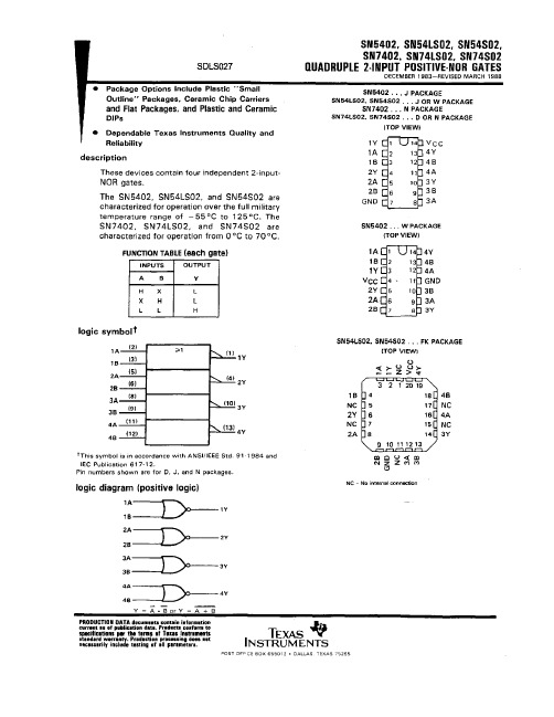
These devices are high speed hex buffers with 3-state outputs. They are organized as single 6-bit or 2-bit / 4-bit, with inverting or non-inverting data (D) paths. The outputs are designed to drive 15 TTL Unit Loads or 60 Low Power Schottky loads when the Enable (E) is LOW. When the Output Enable (E) is HIGH, the outputs are forced to a high impedance “off” state. If the outputs of the 3-state devices are tied together, all but one device must be in the high impedance state to avoid high currents that would exceed the maximum ratings. Designers should ensure that Output Enable signals to 3-state devices whose outputs are tied together are designed so there is no overlap.
2
3
4
5
6
7
8 GND
TRUTH TABLE
INPUTS E1 L L H X E2 L L X H D L H X X L H (Z) (Z) OUTPUT L L H X
74ls00中文资料_数据手册_参数

74LS00包类型包画画引脚包数量生态计划 (2)铅/球完成 MSL峰值温度 (3) SNJ5400W活性 CFP W ^ 14 1没有打电话给TI等级-NCNC-NC SNJ5400WA已过时 CFP WA 14没有打电话给TI等级-NC-NC-NC SNJ54LS00FK活性 LCCC FK 20 1没有打电话给TI等级SNJ54LS00J 活性 CDIP ? 14 1没有打电话给TI等级SNJ54LS00W活性 CFP W ^ 14 1没有打电话给TI等级SNJ54S00FK活性 LCCC FK 20 1没有打电话给TI 等级SNJ54S00J活性 CDIP ? 14 1没有打电话给TI等级74LS00活性 CFP W ^ 14 1没有打电话给TI等级(1) 营销状况值定义如下: ACTIVE:74LS00推荐用于新设计的产品设备. LIFEBUY:TI已经宣布该设备将停产,终身购买期限已经生效. NRND:不建议用于新设 计.器件正在生产中以支持现有客户,但TI不建议使用此74LS00部分一个新的设计.预览:设备已被宣布,但尚未投入生产.样品或提供或 不提供.停产:TI已停止生产该设备. (2) 生态计划 - 目前可能无法使用 - 74LS00请查阅取新的可用性信息和附加信息产品内容细节. 无:尚未提供铅(无铅).无铅(ROHS):TI的术语“无铅”或“无铅”是指符合当前ROHS要求的半导体产品对于所有6种物 质,74LS00包括在均质材料中铅含量不超过0.1%的
SN54LS48FK中文资料

Copyright © 1988, Texas Instruments Incorporated PRODUCTION DATA information is current as of publication date.Products conform to specifications per the terms of Texas Instrumentsstandard warranty. Production processing does not necessarily includetesting of all parameters.11 POST OFFICE BOX 655303 • DALLAS, TEXAS 7526512POST OFFICE BOX 655303 • DALLAS, TEXAS 7526513 POST OFFICE BOX 655303 • DALLAS, TEXAS 75265元器件交易网IMPORTANT NOTICETexas Instruments and its subsidiaries (TI) reserve the right to make changes to their products or to discontinueany product or service without notice, and advise customers to obtain the latest version of relevant informationto verify, before placing orders, that information being relied on is current and complete. All products are soldsubject to the terms and conditions of sale supplied at the time of order acknowledgement, including thosepertaining to warranty, patent infringement, and limitation of liability.TI warrants performance of its semiconductor products to the specifications applicable at the time of sale inaccordance with TI’s standard warranty. Testing and other quality control techniques are utilized to the extentTI deems necessary to support this warranty. Specific testing of all parameters of each device is not necessarilyperformed, except those mandated by government requirements.CERTAIN APPLICATIONS USING SEMICONDUCTOR PRODUCTS MAY INVOLVE POTENTIAL RISKS OFDEATH, PERSONAL INJURY, OR SEVERE PROPERTY OR ENVIRONMENTAL DAMAGE (“CRITICALAPPLICATIONS”). TI SEMICONDUCTOR PRODUCTS ARE NOT DESIGNED, AUTHORIZED, ORWARRANTED TO BE SUITABLE FOR USE IN LIFE-SUPPORT DEVICES OR SYSTEMS OR OTHERCRITICAL APPLICATIONS. INCLUSION OF TI PRODUCTS IN SUCH APPLICATIONS IS UNDERSTOOD TOBE FULLY AT THE CUSTOMER’S RISK.In order to minimize risks associated with the customer’s applications, adequate design and operatingsafeguards must be provided by the customer to minimize inherent or procedural hazards.TI assumes no liability for applications assistance or customer product design. TI does not warrant or representthat any license, either express or implied, is granted under any patent right, copyright, mask work right, or otherintellectual property right of TI covering or relating to any combination, machine, or process in which suchsemiconductor products or services might be or are used. TI’s publication of information regarding any thirdparty’s products or services does not constitute TI’s approval, warranty or endorsement thereof.Copyright © 1999, Texas Instruments Incorporated。
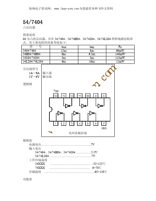
7400中文

54XXX …………………………………. -55~125℃ 74XXX …………………………………. 0~70℃ 存储温度 ………………………………………….-65~150℃
功能表
推荐工作条件
5400/7400
54H00/74H00
54S00/74S00
54LS00/74LS00
单
最小 额定 最大 最小 额定 最大 最小 额定 最大 最小 额定 最大 位
-2
-40 -100 -40 -100
16.8 40
‘S00 最小 最大
-1.2 2.5 2.7
0.5 0.5 1
50
-2 -40 -100 -40 -100
16 36
‘LS00 最小 最大
-1.5 2.5 2.7
0.4 0.5
0.1
20 -0.4
-20 -100 -20 -100
1.6 4.4
单位
40
IIL输入低电平电流 Vcc=最大
VIL=0.4V VIL=0.5V
-1.6
IOS输出短路电流
Vcc=最大
54 -20 -55 74 -18 -55
ICCH输出高电平时电源电流
Vcc=最大
8
ICCL输出低电平时电源电流
Vcc=.5
2.4 2.4
0.4 0.4 1
50
电 源 电 压 54 4.5
5
5.5 4.5
5
5.5 4.5
5
Vcc
74 4.75 5 5.25 4.75 5 5.25 4.75 5
5.5 4.5 5.25 4.75
5 5
5.5 5.25
V
输入高电平电压ViH
SN54LS40W中文资料
Copyright © 1988, Texas Instruments Incorporated PRODUCTION DATA information is current as of publication date.Products conform to specifications per the terms of Texas Instrumentsstandard warranty. Production processing does not necessarily includetesting of all parameters.POST OFFICE BOX 655303 • DALLAS, TEXAS 752652POST OFFICE BOX 655303 • DALLAS, TEXAS 752653 POST OFFICE BOX 655303 • DALLAS, TEXAS 752654POST OFFICE BOX 655303 • DALLAS, TEXAS 752655 POST OFFICE BOX 655303 • DALLAS, TEXAS 75265元器件交易网IMPORTANT NOTICETexas Instruments and its subsidiaries (TI) reserve the right to make changes to their products or to discontinueany product or service without notice, and advise customers to obtain the latest version of relevant informationto verify, before placing orders, that information being relied on is current and complete. All products are soldsubject to the terms and conditions of sale supplied at the time of order acknowledgement, including thosepertaining to warranty, patent infringement, and limitation of liability.TI warrants performance of its semiconductor products to the specifications applicable at the time of sale inaccordance with TI’s standard warranty. Testing and other quality control techniques are utilized to the extentTI deems necessary to support this warranty. Specific testing of all parameters of each device is not necessarilyperformed, except those mandated by government requirements.CERTAIN APPLICATIONS USING SEMICONDUCTOR PRODUCTS MAY INVOLVE POTENTIAL RISKS OFDEATH, PERSONAL INJURY, OR SEVERE PROPERTY OR ENVIRONMENTAL DAMAGE (“CRITICALAPPLICATIONS”). TI SEMICONDUCTOR PRODUCTS ARE NOT DESIGNED, AUTHORIZED, ORWARRANTED TO BE SUITABLE FOR USE IN LIFE-SUPPORT DEVICES OR SYSTEMS OR OTHERCRITICAL APPLICATIONS. INCLUSION OF TI PRODUCTS IN SUCH APPLICATIONS IS UNDERSTOOD TOBE FULLY AT THE CUSTOMER’S RISK.In order to minimize risks associated with the customer’s applications, adequate design and operatingsafeguards must be provided by the customer to minimize inherent or procedural hazards.TI assumes no liability for applications assistance or customer product design. TI does not warrant or representthat any license, either express or implied, is granted under any patent right, copyright, mask work right, or otherintellectual property right of TI covering or relating to any combination, machine, or process in which suchsemiconductor products or services might be or are used. TI’s publication of information regarding any thirdparty’s products or services does not constitute TI’s approval, warranty or endorsement thereof.Copyright © 1999, Texas Instruments Incorporated。
74ls00中文资料_数据手册_参数
74LS00包类型包画画引脚包数量生态计划 (2)铅/球完成 MSL峰值温度 (3) SNJ5400W活性 CFP W ^ 14 1没有打电话给TI等级-NCNC-NC SNJ5400WA已过时 CFP WA 14没有打电话给TI等级-NC-NC-NC SNJ54LS00FK活性 LCCC FK 20 1没有打电话给TI等级SNJ54LS00J 活性 CDIP ? 14 1没有打电话给TI等级SNJ54LS00W活性 CFP W ^ 14 1没有打电话给TI等级SNJ54S00FK活性 LCCC FK 20 1没有打电话给TI 等级SNJ54S00J活性 CDIP ? 14 1没有打电话给TI等级74LS00活性 CFP W ^ 14 1没有打电话给TI等级(1) 营销状况值定义如下: ACTIVE:74LS00推荐用于新设计的产品设备. LIFEBUY:TI已经宣布该设备将停产,终身购买期限已经生效. NRND:不建议用于新设 计.器件正在生产中以支持现有客户,但TI不建议使用此74LS00部分一个新的设计.预览:设备已被宣布,但尚未投入生产.样品或提供或 不提供.停产:TI已停止生产该设备. (2) 生态计划 - 目前可能无法使用 - 74LS00请查阅取新的可用性信息和附加信息产品内容细节. 无:尚未提供铅(无铅).无铅(ROHS):TI的术语“无铅”或“无铅”是指符合当前ROHS要求的半导体产品对于所有6种物 质,74LS00包括在均质材料中铅含量不超过0.1%的要求.在哪里设计焊接在高温下,TI无铅产品适用于特定的无铅工艺.绿色(ROHS和 无SB / BR):TI将“绿色”定义为“无铅”,另外使用不含卤素的包装材料,包括总产品重量的0.1%以上的溴(BR)或锑(SB). (3) MSL,PEAK TEMP. - 根据JEDEC行业标准分类
SNJ54LS00W中文资料
PACKAGING INFORMATIONOrderable Device Status(1)PackageType PackageDrawingPins PackageQtyEco Plan(2)Lead/Ball Finish MSL Peak Temp(3)JM38510/00104BCA ACTIVE CDIP J141None Call TI Level-NC-NC-NC JM38510/00104BDA ACTIVE CFP W141None Call TI Level-NC-NC-NC JM38510/07001BCA ACTIVE CDIP J141None Call TI Level-NC-NC-NC JM38510/07001BDA ACTIVE CFP W141None Call TI Level-NC-NC-NC JM38510/30001B2A ACTIVE LCCC FK201None Call TI Level-NC-NC-NC JM38510/30001BCA ACTIVE CDIP J141None Call TI Level-NC-NC-NC JM38510/30001BDA ACTIVE CFP W141None Call TI Level-NC-NC-NC JM38510/30001SCA ACTIVE CDIP J141None Call TI Level-NC-NC-NC JM38510/30001SDA ACTIVE CFP W141None Call TI Level-NC-NC-NC SN5400J ACTIVE CDIP J141None Call TI Level-NC-NC-NC SN54LS00J ACTIVE CDIP J141None Call TI Level-NC-NC-NC SN54S00J ACTIVE CDIP J141None Call TI Level-NC-NC-NCSN7400D ACTIVE SOIC D1450Pb-Free(RoHS)CU NIPDAU Level-2-260C-1YEAR/Level-1-235C-UNLIMSN7400DR ACTIVE SOIC D142500Pb-Free(RoHS)CU NIPDAU Level-2-260C-1YEAR/Level-1-235C-UNLIMSN7400N ACTIVE PDIP N1425Pb-Free(RoHS)CU NIPDAU Level-NC-NC-NC SN7400N3OBSOLETE PDIP N14None Call TI Call TISN7400NSR ACTIVE SO NS142000Pb-Free(RoHS)CU NIPDAU Level-2-260C-1YEAR/Level-1-235C-UNLIMSN74LS00D ACTIVE SOIC D1450Pb-Free(RoHS)CU NIPDAU Level-2-260C-1YEAR/Level-1-235C-UNLIMSN74LS00DBLE OBSOLETE SSOP DB14None Call TI Call TISN74LS00DBR ACTIVE SSOP DB142000Pb-Free(RoHS)CU NIPDAU Level-2-260C-1YEAR/Level-1-235C-UNLIMSN74LS00DR ACTIVE SOIC D142500Pb-Free(RoHS)CU NIPDAU Level-2-260C-1YEAR/Level-1-235C-UNLIMSN74LS00J OBSOLETE CDIP J14None Call TI Call TISN74LS00N ACTIVE PDIP N1425Pb-Free(RoHS)CU NIPDAU Level-NC-NC-NCSN74LS00NSR ACTIVE SO NS142000Pb-Free(RoHS)CU NIPDAU Level-2-260C-1YEAR/Level-1-235C-UNLIMSN74LS00PSR ACTIVE SO PS82000Pb-Free(RoHS)CU NIPDAU Level-2-260C-1YEAR/Level-1-235C-UNLIMSN74S00D ACTIVE SOIC D1450Pb-Free(RoHS)CU NIPDAU Level-2-260C-1YEAR/Level-1-235C-UNLIMSN74S00DR ACTIVE SOIC D142500Pb-Free(RoHS)CU NIPDAU Level-2-260C-1YEAR/Level-1-235C-UNLIMSN74S00N ACTIVE PDIP N1425Pb-Free(RoHS)CU NIPDAU Level-NC-NC-NC SN74S00N3OBSOLETE PDIP N14None Call TI Call TISN74S00NSR ACTIVE SO NS142000Pb-Free(RoHS)CU NIPDAU Level-2-260C-1YEAR/Level-1-235C-UNLIMSN74S00PSR ACTIVE SO PS82000Pb-Free(RoHS)CU NIPDAU Level-2-260C-1YEAR/Level-1-235C-UNLIMSNJ5400J ACTIVE CDIP J141None Call TI Level-NC-NC-NCOrderable Device Status(1)PackageType PackageDrawingPins PackageQtyEco Plan(2)Lead/Ball Finish MSL Peak Temp(3)SNJ5400W ACTIVE CFP W141None Call TI Level-NC-NC-NCSNJ5400WA OBSOLETE CFP WA14None Call TI Level-NC-NC-NC SNJ54LS00FK ACTIVE LCCC FK201None Call TI Level-NC-NC-NC SNJ54LS00J ACTIVE CDIP J141None Call TI Level-NC-NC-NC SNJ54LS00W ACTIVE CFP W141None Call TI Level-NC-NC-NC SNJ54S00FK ACTIVE LCCC FK201None Call TI Level-NC-NC-NCSNJ54S00J ACTIVE CDIP J141None Call TI Level-NC-NC-NCSNJ54S00W ACTIVE CFP W141None Call TI Level-NC-NC-NC(1)The marketing status values are defined as follows:ACTIVE:Product device recommended for new designs.LIFEBUY:TI has announced that the device will be discontinued,and a lifetime-buy period is in effect.NRND:Not recommended for new designs.Device is in production to support existing customers,but TI does not recommend using this part in a new design.PREVIEW:Device has been announced but is not in production.Samples may or may not be available.OBSOLETE:TI has discontinued the production of the device.(2)Eco Plan-May not be currently available-please check /productcontent for the latest availability information and additional product content details.None:Not yet available Lead(Pb-Free).Pb-Free(RoHS):TI's terms"Lead-Free"or"Pb-Free"mean semiconductor products that are compatible with the current RoHS requirements for all6substances,including the requirement that lead not exceed0.1%by weight in homogeneous materials.Where designed to be soldered at high temperatures,TI Pb-Free products are suitable for use in specified lead-free processes.Green(RoHS&no Sb/Br):TI defines"Green"to mean"Pb-Free"and in addition,uses package materials that do not contain halogens, including bromine(Br)or antimony(Sb)above0.1%of total product weight.(3)MSL,Peak Temp.--The Moisture Sensitivity Level rating according to the JEDECindustry standard classifications,and peak solder temperature.Important Information and Disclaimer:The information provided on this page represents TI's knowledge and belief as of the date that it is provided.TI bases its knowledge and belief on information provided by third parties,and makes no representation or warranty as to the accuracy of such information.Efforts are underway to better integrate information from third parties.TI has taken and continues to take reasonable steps to provide representative and accurate information but may not have conducted destructive testing or chemical analysis on incoming materials and chemicals.TI and TI suppliers consider certain information to be proprietary,and thus CAS numbers and other limited information may not be available for release.In no event shall TI's liability arising out of such information exceed the total purchase price of the TI part(s)at issue in this document sold by TI to Customer on an annual basis.元器件交易网元器件交易网IMPORTANT NOTICETexas Instruments Incorporated and its subsidiaries (TI) reserve the right to make corrections, modifications,enhancements, improvements, and other changes to its products and services at any time and to discontinueany product or service without notice. Customers should obtain the latest relevant information before placingorders and should verify that such information is current and complete. All products are sold subject to TI’s termsand conditions of sale supplied at the time of order acknowledgment.TI warrants performance of its hardware products to the specifications applicable at the time of sale inaccordance with TI’s standard warranty. T esting and other quality control techniques are used to the extent TIdeems necessary to support this warranty. Except where mandated by government requirements, testing of allparameters of each product is not necessarily performed.TI assumes no liability for applications assistance or customer product design. Customers are responsible fortheir products and applications using TI components. T o minimize the risks associated with customer productsand applications, customers should provide adequate design and operating safeguards.TI does not warrant or represent that any license, either express or implied, is granted under any TI patent right,copyright, mask work right, or other TI intellectual property right relating to any combination, machine, or processin which TI products or services are used. Information published by TI regarding third-party products or servicesdoes not constitute a license from TI to use such products or services or a warranty or endorsement thereof.Use of such information may require a license from a third party under the patents or other intellectual propertyof the third party, or a license from TI under the patents or other intellectual property of TI.Reproduction of information in TI data books or data sheets is permissible only if reproduction is withoutalteration and is accompanied by all associated warranties, conditions, limitations, and notices. Reproductionof this information with alteration is an unfair and deceptive business practice. TI is not responsible or liable forsuch altered documentation.Resale of TI products or services with statements different from or beyond the parameters stated by TI for thatproduct or service voids all express and any implied warranties for the associated TI product or service andis an unfair and deceptive business practice. TI is not responsible or liable for any such statements.Following are URLs where you can obtain information on other Texas Instruments products and applicationsolutions:Products ApplicationsAmplifiers Audio /audioData Converters Automotive /automotiveDSP Broadband /broadbandInterface Digital Control /digitalcontrolLogic Military /militaryPower Mgmt Optical Networking /opticalnetworkMicrocontrollers Security /securityTelephony /telephonyVideo & Imaging /videoWireless /wirelessMailing Address:Texas InstrumentsPost Office Box 655303 Dallas, Texas 75265Copyright 2005, Texas Instruments Incorporated。
芯片引脚图
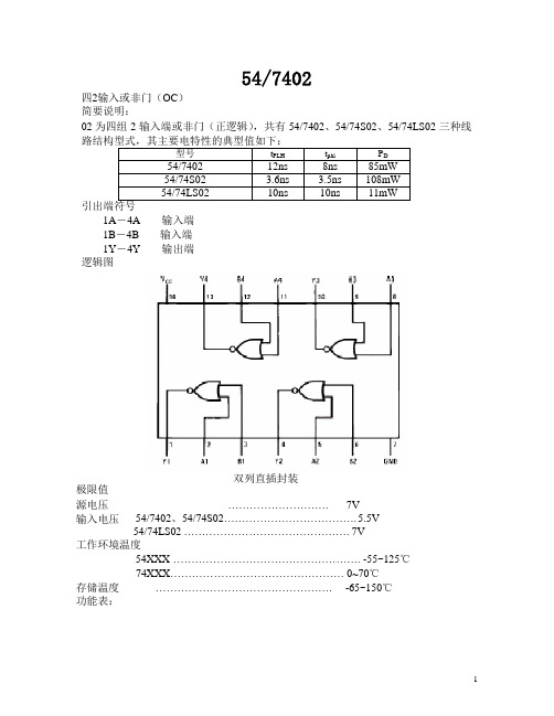
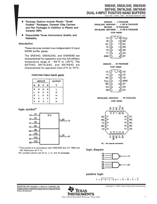
54/7402四2输入或非门(OC)简要说明:02 为四组2 输入端或非门(正逻辑),共有54/7402、54/74S02、54/74LS02 三种线1A-4A 输入端1B-4B 输入端1Y-4Y 输出端逻辑图双列直插封装极限值源电压 (7V)输入电压54/7402、54/74S02……………………………….5.5V54/74LS02 (7V)工作环境温度54XXX ……………………………………………. -55~125℃74XXX………………………………………… 0~70℃存储温度………………………………………….-65~150℃功能表:74LS00四2输入与非门简要说明00 为四组2 输入端与非门(正逻辑),共有 54/7400、54/74H00、54/74S00、54/74LS001A-4A,1B-4B 输入端1Y-4Y 输出端逻辑图双列直插封装极限值电源电压 (7V)输入电压 54/7400、54/74H00、54/74S00…………….5.5V54/74LS00 (7V)A-B 间电压除 54/74LS00 外………………………………5.5V工作环境温度 54XXX …………………. -55~125℃74XXX …………………. 0~70℃存储温度………………………………………….-65~150℃功能表:54/7408四2输入与门简要说明08 为四组2 输入端与门(正逻辑),共有54/7408、54/74S08、54/74LS08 三种线路1A-4A 输入端1B-4B 输入端1Y-4Y 输出端双列直插封装极限值电源电压 (7V)输入电压 54/7408、54/74S08……………………………… 5.5V54/74LS08 (7V)A-B 间电压 54/7408、54/74S08………………………………5.5V输出截止态电压 (7V)工作环境温度 54XXX ……………………………………………. -55~125℃ 74XXX………………………………………… 0~70℃存储温度…………………………………………. -65~150℃功能表:54/7420双4输入与非门简要说明20 为两组4 输入端与非门(正逻辑),共有54/7420、54/74H20、54/74S20、54/74LS20引出端符号1A,2A 输入端1B,2B 输入端1C,2C 输入端1D,2D 输入端1Y,2Y 输出端逻辑图双列直插封装极限值电源电压 (7V)输入电压54/7420、54/74H20、54/74S20…………….5.5V54/74LS20 (7V)A-B-C-D 间电压除54/74LS20 外………………………………5.5V工作环境温度54XXX ………………………………….-55~125℃74XXX ……………………….0~70℃存储温度………………………………65~150℃功能表:54/7454四路输入与或非门 简要说明54 为与或非门(正逻辑),其中 54/7454 是 2-2-2-2 输入端,54/74H54 是 2-2 -3-引出端符号A -H (‘H54 为 I ,’LS 为 J ) 输入端Y 输出端逻辑图54/7454 双列直插封装 ‘LS54 双列直插封装 ‘LS54PLCC 封装极限值电源电压 (7V)输入电压54/7454…………………………………………. 5.5V54/74LS54 (7V)A-B,C-D,E-F,G-H 间电压54/7454…………………………………………. 5.5V工作环境温度54XXX ……………………………………………. -55~545℃74XXX………………………………………… 0~70℃存储温度………………………………………….-65~150℃原理图:74ls13874HC138管脚图:74LS138 为3 线-8 线译码器,共有 54/74S138和54/74LS138 两种线路结构型式,其工作原理如下:当一个选通端(G1)为高电平,另两个选通端(/(G2A)和/(G2B))为低电平时,可将地址端(A、B、C)的二进制编码在一个对应的输出端以低电平译出。
74ls00
测试条件
tPLH 传输延迟 tPHL 传输延迟
A或B A或B
Y Y
CL=15pF RL=2kΩ
最小
参数值 典型
9 10
最大 15 15
单位
ns ns
天水天光半导体有限责任公司(八七一厂) 2005.1 版
电 性 能:(除特别说明外,均为全温度范围)
74Ⅱ
符号 参数名称
测试条件
参数值
最小 典型 最大
VIK 输入钳位电压
Vcc=最小 II=-18mA
VOH 输出高电平电压
Vcc=最小 VIL=最大 2.7 IOH=最大
VOL 输出低电平电压
Vcc=最小 VIH=2V IOL=最大
输入电流 II (最大输入电压时) Vcc=最大 VI=7V
典型参数:
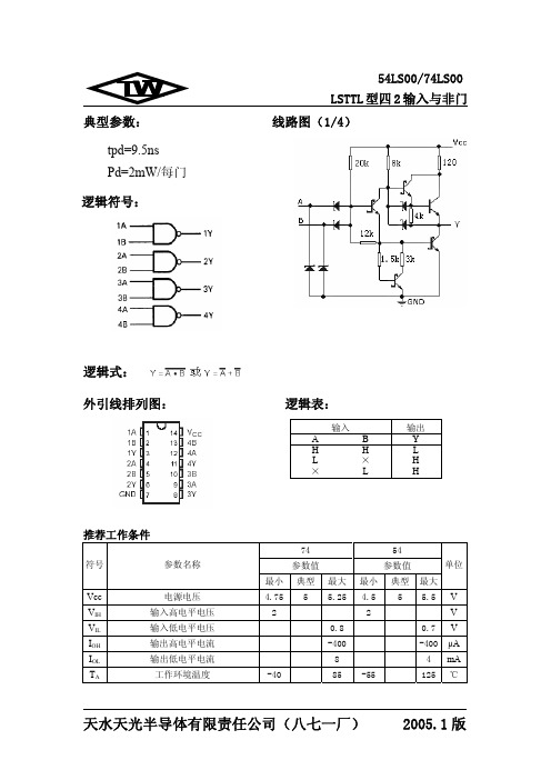
tpd=9.5ns Pd=2mW/每门 逻辑符号:
54LS00/74LS00 LSTTL 型四 2 输入与非门 线路图(1/4)
逻辑式: 外引线排列图:
逻辑表:
输入
A
B
H
H
L
×
×
L
输出 Y L H H
推荐工作条件
符号
参数名称
Vcc
电源电压
VIH
输入高电平电压
VIL
输入低电平电压
IOH
输出高电平电流
-1.5
0.5 0.1
IIH 输入高电平电流 Vcc=最大 VI=2.7V
IIL 输入低电平电流 Vcc=最大 VI=0.4V
IOS 输出短路电流
Vcc=最大 VO=0V -20
ICCH 高电平电源电流 Vcc=最大 VI=0V
ICCL 低电平电源电流 Vcc=最大 输入开路
74HC00中文资料

单位
ns ns
参数
tPLH输出由低到高传输延迟时间 tPHL输出由高到低传输延迟时间
测试条件
Vcc =5V,CL=50Pf(‘H00 为 25Pf) RL=400Ω(‘H00 和‘S00 为 260Ω,
‘LS00 为 2KΩ
‘00 最大
22
15
‘H00 最大
10
10
‘S00 最大 4.5
5
‘LS00 最大 15
15
54S00/74S00
54LS00/74LS00
单
最小 额定 最大 最小 额定 最大 最小 额定 最大 最小 额定 最大 位
电 源 电 压 54 4.5
5
5.5 4.5
5
5.5 4.5
5
Vcc
74 4.75 5 5.25 4.75 5 5.25 4.75 5
5.5 4.5 5.25 4.75
5 5
5.5 5.25
Vcc=最大
VI=5.5V VI=7V
1
IIH输入高电平电流 Vcc=最大
VIH=2.4V VIH=2.7V
40
IIL输入低电平电流 Vcc=最大
VIL=0.4V VIL=0.5V
-1.6
IOS输出短路电流
Vcc=最大
54 -20 -55 74 -18 -55
ICCH输出高电平时电源电流
Vcc=最大
海纳电子资讯网:www.fpga-arm.com 为您提供各种IC中文资料
54XXX …………………………………. -55~125℃ 74XXX …………………………………. 0~70℃ 存储温度 ………………………………………….-65~150℃ 功能表
- 1、下载文档前请自行甄别文档内容的完整性,平台不提供额外的编辑、内容补充、找答案等附加服务。
- 2、"仅部分预览"的文档,不可在线预览部分如存在完整性等问题,可反馈申请退款(可完整预览的文档不适用该条件!)。
- 3、如文档侵犯您的权益,请联系客服反馈,我们会尽快为您处理(人工客服工作时间:9:00-18:30)。
Original Creation Date: 04/23/98Last Update Date: 05/14/98Last Major Revision Date: 04/23/98MNDM54LS00-X REV 1A0MICROCIRCUIT DATA SHEETQUAD 2-INPUT NAND GATEGeneral DescriptionThis device contains four independent gates, each of which performs the logic NAND function.NS Part NumbersDM54LS00E/883DM54LS00J/883DM54LS00W/883Industry Part Number54LS00Prime DieL000ProcessingMIL-STD-883, Method 5004Quality Conformance InspectionMIL-STD-883, Method 5005Subgrp Description Temp ( C)o 1Static tests at +252Static tests at +1253Static tests at -554Dynamic tests at +255Dynamic tests at +1256Dynamic tests at -557Functional tests at +258A Functional tests at +1258B Functional tests at -559Switching tests at +2510Switching tests at +12511Switching tests at-55MICROCIRCUIT DATA SHEET MNDM54LS00-X REV 1A0FeaturesMICROCIRCUIT DATA SHEET MNDM54LS00-X REV 1A0(Absolute Maximum Ratings)(Note 1)Storage Temperature-65 C to +150 CAmbient Temperature under Bias-55 C to +125 CInput Voltage-0.5V to +10.0VVCC Pin Potential to Ground Pin-0.5V to +7.0VJunction Temperature under Bias-55 C to +175 CCurrent Applied to Output in LOW state (Max)twice the rated Iol (ma)Note 1:Absolute Maximum ratings are those values beyond which the device may be damaged or have its useful life impaired. Functional operation under these conditions is notimplied.Recommended Operating ConditionsFree Air Ambient TemperatureMilitary-55 C to +125 CSupply VoltageMilitary+4.5V to +5.5VMNDM54LS00-X REV 1A0MICROCIRCUIT DATA SHEETElectrical CharacteristicsDC PARAMETER(The following conditions apply to all the following parameters, unless otherwise specified.)DC:VCC 4.5V to 5.5V, Temp range: -55C to 125CSYMBOL PARAMETER CONDITIONS NOTES PIN-NAME MIN MAX UNITSUB-GROUPSIIH Input HighCurrent VCC=5.5V, VM=2.7V, VINH=4.5V,VINL=0.0V1, 3INPUTS20.0uA1, 2,3IBVI Input HighCurrent VCC=5.5V, VM=10.0V, VINH=4.5V,VINL=0.0V1, 3INPUTS100uA1, 2,3IIL Input LOW Current VCC=5.5V, VM=0.4V, VINH=4.5V1, 3INPUTS-0.03-0.4mA1, 2,3VOL Output LOWVoltage VCC=4.5V, VIH=2.0V, IOL=4.0mA,VINH=4.5V1, 3OUTPUTS0.4V1, 2,3VOH Output HIGHVoltage VCC=4.5V, VIL=0.7V, IOH=-0.4mA,VINH=4.5V1, 3OUTPUTS 2.5V1, 2,3IOS Short-CircuitCurrent VCC=5.5V, VINL=0.0V, VOUT=0.0V1, 3OUTPUTS-20-100mA1, 2,3VCD Input Clamp DiodeVoltage VCC=4.5V, IM=-18mA, VINH=4.5V1, 3INPUTS-1.5V1, 2,3ICCH Supply Current VCC=5.5V, VINL=0.0V1, 3VCC 1.6mA1, 2,3ICCL Supply Current VCC=5.5V, VINH=4.5V1, 3VCC 4.4mA1, 2,3AC PARAMETER - 15pF(The following conditions apply to all the following parameters, unless otherwise specified.)AC:CL=15pF, RL=2k ohms Temp range: +25CtpLH Propagation Delay VCC=5.0V5In toOn10.0ns9tpHL Propagation Delay VCC=5.0V5In toOn10.0ns9AC PARAMETER - 50pF(The following conditions apply to all the following parameters, unless otherwise specified.)AC:CL=50pF, RL=2k ohms Temp range: -55C to +125CtpLH Propagation Delay VCC=5.0V2, 4In toOn2.015.0ns92, 4In toOn2.020.0ns10, 11tpHL Propagation Delay VCC=5.0V2, 4In toOn2.017.0ns92, 4In toOn2.024.0ns10, 11Note 1:Screen tested 100% on each device at -55C, +25C & +125C temperature, subgroups A1, 2, 3, 7 & 8.Note 2:Screen tested 100% on each device at +25C temperature only, subgroup A9.MNDM54LS00-X REV 1A0MICROCIRCUIT DATA SHEET(Continued)Note 3:Sample tested (Method 5005, Table 1) on each MFG. lot at +25C, +125C & -55Ctemperature, subgroups A1, 2, 3, 7 & 8.Note 4:Sample tested (Method 5005, Table 1) on each MFG. lot at +25C, subgroup A9.Subgroups 10 & 11 are guaranteed, not tested.Note 5:Guaranteed, not tested.MICROCIRCUIT DATA SHEET MNDM54LS00-X REV 1A0Revision HistoryRev ECN #Rel Date Originator Changes1A0M000120005/14/98Linda Collins Initial release: MNDM54LS00-X Rev. 1A0Added note 4 tothe AC (50pF) notes reference column.Reworded note 4from "and periodically at +125C & -55C,subgroups 10 &11" to "Subgroups 10 & 11 are guaranteed, nottested".Changed the VOL test condition from VIL=2.0Vto VIH=2.0V.。