HD74HC27RPEL中文资料
HD74HC375P中文资料

HD74HC375Quad. Bistable LatchesADE-205-500 (Z)1st. EditionSep. 2000 DescriptionThis latch is ideally suited for use as temporary storage for binary information between processing units and input/output or indicator units. Information present at a data (D) input is transferred to the Q output when the enable (G) is high and the Q output will follow the data input as long as the enable remains high. When the enable goes low, the information (that was present at the data input at the time the transition occurred) is retained at the Q output until the enable goes high.Features• High Speed Operation: t pd (Data to Q, Q) = 10 ns typ (C L = 50 pF)• High Output Current: Fanout of 10 LSTTL Loads• Wide Operating Voltage: V CC = 2 to 6 V• Low Input Current: 1 µA max• Low Quiescent Supply Current: I CC (static) = 4 µA max (Ta = 25°C)Function TableInputs OutputsD G Q QL H L HH H H LX L no change no changeHD74HC375 Pin Arrangement2HD74HC3753DC CharacteristicsTa = 25°CTa = –40 to +85°CItem Symbol V CC (V)Min Typ Max MinMax Unit Test ConditionsInput voltageV IH2.0 1.5—— 1.5—V4.5 3.15—— 3.15—6.04.2—— 4.2—V IL2.0——0.5—0.5V 4.5—— 1.35—1.356.0——1.8— 1.8Output voltageV OH2.0 1.9 2.0— 1.9—VVin = V IH or V IL I OH = –20 µA4.5 4.4 4.5— 4.4—6.05.96.0— 5.9—4.5 4.18—— 4.13—I OH = –4 mA 6.05.68——5.63—I OH = –5.2 mAV OL2.0—0.00.1—0.1VVin = V IH or V IL I OL = 20 µA4.5—0.00.1—0.16.0—0.00.1—0.14.5——0.26—0.33I OL = 4 mA 6.0——0.26—0.33I OL = 5.2 mAInput current Iin 6.0——±0.1—±1.0µA Vin = V CC or GNDQuiescent supply currentI CC6.0——4.0—40µAVin = V CC or GND, Iout = 0 µAHD74HC3754AC Characteristics (C L = 50 pF, Input t r = t f = 6 ns)Ta = 25°CTa = –40 to +85°CItem Symbol V CC (V)Min Typ Max MinMax Unit Test Conditions Propagation delay t PLH2.0——145—180nsData to Q or Qtimet PHL 4.5—1029—366.0——25—31t PLH 2.0——160—200nsG to Q or Qt PHL4.5—1132—406.0——27—34Pulse widtht w2.080——100—ns 4.5165—20—6.014——17—Setup timet su2.0100——125—ns 4.5202—25—6.017——21—Hold timet h2.05——5—ns 4.55–1—5—6.05——5—Output rise/fall t TLH 2.0——75—95ns timet THL 4.5—515—196.0——13—16Input capacitanceCin——510—10pFHD74HC375 Package Dimensions5HD74HC3756HD74HC3757Cautions1.Hitachi neither warrants nor grants licenses of any rights of Hitachi’s or any third party’s patent,copyright, trademark, or other intellectual property rights for information contained in this document.Hitachi bears no responsibility for problems that may arise with third party’s rights, includingintellectual property rights, in connection with use of the information contained in this document.2.Products and product specifications may be subject to change without notice. Confirm that you have received the latest product standards or specifications before final design, purchase or use.3.Hitachi makes every attempt to ensure that its products are of high quality and reliability. However,contact Hitachi’s sales office before using the product in an application that demands especially high quality and reliability or where its failure or malfunction may directly threaten human life or cause risk of bodily injury, such as aerospace, aeronautics, nuclear power, combustion control, transportation,traffic, safety equipment or medical equipment for life support.4.Design your application so that the product is used within the ranges guaranteed by Hitachi particularly for maximum rating, operating supply voltage range, heat radiation characteristics, installationconditions and other characteristics. Hitachi bears no responsibility for failure or damage when used beyond the guaranteed ranges. Even within the guaranteed ranges, consider normally foreseeable failure rates or failure modes in semiconductor devices and employ systemic measures such as fail-safes, so that the equipment incorporating Hitachi product does not cause bodily injury, fire or other consequential damage due to operation of the Hitachi product.5.This product is not designed to be radiation resistant.6.No one is permitted to reproduce or duplicate, in any form, the whole or part of this document without written approval from Hitachi.7.Contact Hitachi’s sales office for any questions regarding this document or Hitachi semiconductor products.Hitachi, Ltd.Semiconductor & Integrated Circuits.Nippon Bldg., 2-6-2, Ohte-machi, Chiyoda-ku, Tokyo 100-0004, Japan Tel: Tokyo (03) 3270-2111 Fax: (03) 3270-5109Copyright © Hitachi, Ltd., 2000. All rights reserved. Printed in Japan.Hitachi Asia Ltd. Hitachi Tower16 Collyer Quay #20-00, Singapore 049318Tel : <65>-538-6533/538-8577 Fax : <65>-538-6933/538-3877URL : .sg URLNorthAmerica : /Europe : /hel/ecg Asia : Japan : http://www.hitachi.co.jp/Sicd/indx.htmHitachi Asia Ltd.(Taipei Branch Office)4/F, No. 167, Tun Hwa North Road, Hung-Kuo Building, Taipei (105), Taiwan Tel : <886>-(2)-2718-3666 Fax : <886>-(2)-2718-8180 Telex : 23222 HAS-TPURL : Hitachi Asia (Hong Kong) Ltd. Group III (Electronic Components) 7/F., North Tower, World Finance Centre,Harbour City, Canton Road Tsim Sha Tsui, Kowloon, Hong KongTel : <852>-(2)-735-9218 Fax : <852>-(2)-730-0281URL : Hitachi Europe Ltd.Electronic Components Group.Whitebrook ParkLower Cookham Road MaidenheadBerkshire SL6 8YA, United Kingdom Tel: <44> (1628) 585000Fax: <44> (1628) 585160Hitachi Europe GmbHElectronic Components Group Dornacher Stra βe 3D-85622 Feldkirchen, Munich GermanyTel: <49> (89) 9 9180-0Fax: <49> (89) 9 29 30 00Hitachi Semiconductor (America) Inc.179 East Tasman Drive,San Jose,CA 95134 Tel: <1> (408) 433-1990Fax: <1>(408) 433-0223For further information write to:Colophon 2.0。
HD74LV27ARPEL中文资料

HD74LV27ATriple 3-input Positive NOR GatesREJ03D0238–0300Z(Previous ADE-205-256A (Z))Rev.3.00Jun. 01, 2004 DescriptionThe HD74LV27A performs the Boolean functions Y = A•B•C or Y = A+B+C in positive logic.Low-voltage and high-speed operation is suitable for the battery-powered products (e.g., notebook computers), and the low-power consumption extends the battery life.Features•V CC = 2.0 V to 5.5 V operation•All inputs V IH (Max.) = 5.5 V (@V CC = 0 V to 5.5 V)•All outputs V O (Max.) = 5.5 V (@V CC = 0 V)•Typical V OL ground bounce < 0.8 V (@V CC = 3.3 V, Ta = 25°C)•Typical V OH undershoot > 2.3 V (@V CC = 3.3 V, Ta = 25°C)•Output current ±6 mA (@V CC = 3.0 V to 3.6 V), ±12 mA (@V CC = 4.5 V to 5.5 V)•Ordering InformationPart Name Package Type Package Code PackageAbbreviation Taping Abbreviation (Quantity)HD74LV27AFPEL SOP–14 pin(JEITA)FP–14DAV FP EL (2,000 pcs/reel) HD74LV27ARPEL SOP–14 pin(JEDEC)FP–14DNV RP EL (2,500 pcs/reel) HD74LV27ATELL TSSOP–14 pin TTP–14DV T ELL (2,000 pcs/reel) Note: Please consult the sales office for the above package availability.Function TableInputsA B C Output YH X X LX H X LX X H LL L L HNote:H: High levelL: Low levelX: ImmaterialPin ArrangementAbsolute Maximum RatingsItemSymbol Ratings Unit ConditionsSupply voltage range V CC –0.5 to 7.0V Input voltage range*V I –0.5 to 7.0V –0.5 to V CC + 0.5Output: H or L Output voltage range*V O–0.5 to 7.0V V CC : OFF Input clamp current I IK –20mA V I < 0Output clamp currentI OK ±50mA V O < 0 or V O > V CC Continuous output current I O±25mA V O = 0 to V CCContinuous current through V CC or GNDI CC or I GND ±50mA P T 785SOP Maximum power dissipation atTa = 25°C (in still air)*3500mW TSSOPStorage temperatureTstg–65 to 150°CNotes:The absolute maximum ratings are values, which must not be individually be exceeded, and furthermore, no twoof which may be realized at the same time.1.The input and output voltage ratings may be exceeded even if the input and output clamp-current ratings areobserved.2.This value is limited to 5.5 V maximum.3.The maximum package power dissipation was calculated using a junction temperature of 150°C.Recommended Operating ConditionsItemSymbol Min Max Unit ConditionsSupply voltage range V CC 2.0 5.5V Input voltage range V I 0 5.5V Output voltage range V O 0V CC V —–50µA V CC = 2.0 V—–2V CC = 2.3 to 2.7 V —–6V CC = 3.0 to 3.6 V I OH—–12mAV CC = 4.5 to 5.5 V —50µA V CC = 2.0 V—2V CC = 2.3 to 2.7 V —6V CC = 3.0 to 3.6 V Output currentI OL—12mAV CC = 4.5 to 5.5 V 0200V CC = 2.3 to 2.7 V 0100V CC = 3.0 to 3.6 V Input transition rise or fall rate ∆t /∆v 020ns/VV CC = 4.5 to 5.5 VOperating free-air temperature Ta –4085°CNote:Unused or floating inputs must be held high or low.Logic DiagramDC Electrical CharacteristicsTa = –40 to 85°CItem Symbol V CC (V)*Min Typ Max Unit Test Conditions2.01.5——2.3 to 2.7V CC × 0.7——3.0 to 3.6V CC × 0.7——V IH4.5 to5.5V CC × 0.7——2.0——0.52.3 to 2.7——V CC × 0.33.0 to 3.6——V CC × 0.3Input voltageV IL4.5 to5.5——V CC × 0.3VMin to Max V CC – 0.1——I OH = –50 µA 2.3 2.0——I OH = –2 mA 3.0 2.48——I OH = –6 mA V OH 4.53.8——I OH = –12 mA Min to Max ——0.1I OL = 50 µA 2.3——0.4I OL = 2 mA 3.0——0.44I OL = 6 mA Output voltage V OL4.5——0.55VI OL = 12 mAInput currentI IN 0 to 5.5——±1µA V IN = 5.5 V or GNDQuiescent supply current I CC 5.5——20µA V IN = V CC or GND, I O = 0Output leakage currentI OFF 0——5µA V I or V O = 0 V to 5.5 V Input capacitanceC IN3.3—3.5—pFV I = V CC or GNDNote:For conditions shown as Min or Max, use the appropriate values under recommended operating conditions.Switching CharacteristicsV CC = 2.5 ± 0.2 VTa = 25°CTa = –40 to 85°C Item Symbol Min Typ Max Min Max Unit TestConditions FROM (Input)TO(Output)—8.313.8 1.016.0C L = 15 pF Propagation delay timet PLH t PHL—10.017.51.021.0nsC L = 50 pFA, B,or CYV CC = 3.3 ± 0.3 VTa = 25°CTa = –40 to 85°C Item Symbol Min Typ Max Min Max Unit TestConditions FROM (Input)TO(Output)— 6.28.8 1.010.5C L = 15 pF Propagation delay timet PLH t PHL—8.712.31.014.0nsC L = 50 pFA, B,or CYV CC = 5.0 ± 0.5 VTa = 25°C Ta = –40 to 85°C Item Symbol Min Typ Max Min Max Unit TestConditions FROM (Input)TO(Output)— 4.1 5.9 1.07.0C L = 15 pF Propagation delay timet PLH t PHL—5.67.91.09.0nsC L = 50 pFA, B,or CYOperating CharacteristicsC L = 50 pFTa = 25°CItem Symbol V CC (V)Min Typ Max Unit Test ConditionspF f = 10 MHzPower dissipation capacitance C PD3.3—9.5—5.0—11.0—Noise CharacteristicsC L = 50 pFTa = 25°CItem Symbol V CC (V)Min Typ Max Unit Test ConditionsV OL (P) 3.3—0.20.8VQuiet output, maximumdynamic V OLV OL (V) 3.3—–0.1–0.8VQuiet output, minimumdynamic V OLV OH (V) 3.3— 3.2—VQuiet output, minimumdynamic V OHV IH (D) 3.3 2.31——VHigh-level dynamic inputvoltageV IL (D) 3.3——0.99VLow-level dynamic inoutvoltageTest CircuitPackage Dimensions RENESAS SALES OFFICESRenesas Technology America, Inc.450 Holger Way, San Jose, CA 95134-1368, U.S.ATel: <1> (408) 382-7500 Fax: <1> (408) 382-7501Renesas Technology Europe Limited.Dukes Meadow, Millboard Road, Bourne End, Buckinghamshire, SL8 5FH, United KingdomTel: <44> (1628) 585 100, Fax: <44> (1628) 585 900Renesas Technology Europe GmbHDornacher Str. 3, D-85622 Feldkirchen, GermanyTel: <49> (89) 380 70 0, Fax: <49> (89) 929 30 11Renesas Technology Hong Kong Ltd.7/F., North Tower, World Finance Centre, Harbour City, Canton Road, Hong KongTel: <852> 2265-6688, Fax: <852> 2375-6836Renesas Technology Taiwan Co., Ltd.FL 10, #99, Fu-Hsing N. Rd., Taipei, TaiwanTel: <886> (2) 2715-2888, Fax: <886> (2) 2713-2999Renesas Technology (Shanghai) Co., Ltd.26/F., Ruijin Building, No.205 Maoming Road (S), Shanghai 200020, ChinaTel: <86> (21) 6472-1001, Fax: <86> (21) 6415-2952Renesas Technology Singapore Pte. Ltd.1, Harbour Front Avenue, #06-10, Keppel Bay Tower, Singapore 098632Tel: <65> 6213-0200, Fax: <65> 6278-8001Colophon .1.0。
HD74HC240P中文资料

HD74HC240Octal Buffers/Line Drivers/Line Receivers(with inverted 3-state outputs)REJ03D0594–0200(Previous ADE-205-471)Rev.2.00Jan 31, 2006 DescriptionThe HD74HC240 is an inverting buffer and has two active low enables (1G and 2G). Each enable independently controls 4 buffers. This device does not have schmitt trigger inputs.Features• High Speed Operation: t pd = 10 ns typ (C L = 50 pF)• High Output Current: Fanout of 15 LSTTL Loads• Wide Operating Voltage: V CC = 2 to 6 V• Low Input Current: 1 µA max• Low Quiescent Supply Current: I CC (static) = 4 µA max (Ta = 25°C)• Ordering InformationPart Name Package TypePackage Code(Previous Code)PackageAbbreviationTaping Abbreviation(Quantity)HD74HC240P DILP-20pin PRDP0020AC-B(DP-20NEV)P —HD74HC240FPEL SOP-20 pin (JEITA) PRSP0020DD-B(FP-20DAV)FP EL (2,000 pcs/reel)HD74HC240RPEL SOP-20 pin (JEDEC) PRSP0020DC-A(FP-20DBV)RP EL (1,000 pcs/reel)HD74HC240TELL TSSOP-20pin PTSP0020JB-A(TTP-20DAV)T ELL (2,000 pcs/reel)Note: Please consult the sales office for the above package availability.Function TableInputs OutputG A YH X ZL H LL L HH : high levelL : low levelX : irrelevantZ : off (high-impedance) state of a 3-state outputPin ArrangementLogic DiagramAbsolute Maximum RatingsItem Symbol Ratings UnitSupply voltage range V CC –0.5 to 7.0 V Input / Output voltage V IN , V OUT –0.5 to V CC +0.5 V Input / Output diode current I IK , I OK ±20 mA Output current I O ±35 mA V CC , GND current I CC or I GND ±75 mA Power dissipation P T 500 mW Storage temperature Tstg –65 to +150 °C Note: The absolute maximum ratings are values, which must not individually be exceeded, and furthermore, no two ofwhich may be realized at the same time.Recommended Operating ConditionsItem Symbol Ratings Unit ConditionsSupply voltage V CC 2 to 6 V Input / Output voltage V IN , V OUT 0 to V CC V Operating temperature Ta –40 to 85 °C 0 to 1000 V CC = 2.0 V0 to 500 V CC = 4.5 V Input rise / fall time *1 t r , t f 0 to 400 ns V CC = 6.0 V Notes: 1. This item guarantees maximum limit when one input switches.Waveform: Refer to test circuit of switching characteristics.Electrical CharacteristicsTa = 25°C Ta = –40 to+85°CItem Symbol V CC (V)Min Typ Max Min MaxUnitTest Conditions2.0 1.5 — — 1.5— 4.5 3.15 — — 3.15 — V IH6.0 4.2 — — 4.2 —V 2.0 — — 0.5 — 0.5 4.5 — — 1.35 — 1.35Input voltageV IL6.0 — — 1.8 — 1.8V 2.0 1.9 2.0 — 1.9 — 4.5 4.4 4.5 — 4.4 — 6.0 5.9 6.0 — 5.9 — I OH = –20 µA 4.5 4.18 — — 4.13 — I OH = –6 mA V OH6.0 5.68 — — 5.63— V Vin = V IH or V IL I OH = –7.8 mA2.0 — 0.0 0.1 —0.1 4.5 — 0.0 0.1 — 0.1 6.0 — 0.0 0.1 — 0.1 I OL = 20 µA 4.5 — — 0.26 — 0.33 I OL = 6 mA Output voltage V OL6.0 — — 0.26 —0.33 V Vin = V IH or V IL I OL = 7.8 mA Off-state output currentI OZ 6.0— — ±0.5 — ±5.0 µA Vin = V IH or V IL ,Vout = V CC or GNDInput current Iin 6.0 — — ±0.1 — ±1.0 µA Vin = V CC or GNDQuiescent supply current I CC 6.0— — 4.0 — 40 µA Vin = V CC or GND, Iout = 0 µASwitching Characteristics(C L = 50 pF, Input t r = t f = 6 ns)Ta = 25°C Ta = –40 to +85°CItem Symbol V CC (V)Min Typ Max Min MaxUnitTest Conditions2.0 — — 90 — 115 4.5 — 10 18 — 23 t PHL6.0 — — 15 — 20 ns 2.0 — — 90 — 115 4.5 — 10 18 — 23 Propagation delaytimet PLH6.0 — — 15 — 20 ns 2.0 — — 150 — 190 4.5 — 11 30 — 38 t ZL6.0 — — 26 — 33 ns 2.0 — — 150 — 190 4.5 — 12 30 — 38 Output enable time t ZH6.0 — — 26 — 33 ns 2.0 — — 150 — 190 4.5 — 16 30 — 38 t LZ6.0 — — 26 — 33 ns 2.0 — — 150 — 190 4.5 — 19 30 — 38 Output disabletimet HZ6.0 — — 26 —33 ns 2.0 — — 60 —75 4.5 — 4 12 — 15 Output rise/fall timet TLH t THL 6.0 — — 10 — 13 ns Input capacitance Cin— — 5 10—10 pFTest CircuitWaveformsPackage Dimensions RENESAS SALES OFFICESRefer to "/en/network" for the latest and detailed information.Renesas Technology America, Inc.450 Holger Way, San Jose, CA 95134-1368, U.S.ATel: <1> (408) 382-7500, Fax: <1> (408) 382-7501Renesas Technology Europe LimitedDukes Meadow, Millboard Road, Bourne End, Buckinghamshire, SL8 5FH, U.K.Tel: <44> (1628) 585-100, Fax: <44> (1628) 585-900Renesas Technology (Shanghai) Co., Ltd.Unit 205, AZIA Center, No.133 Yincheng Rd (n), Pudong District, Shanghai 200120, ChinaTel: <86> (21) 5877-1818, Fax: <86> (21) 6887-7898Renesas Technology Hong Kong Ltd.7th Floor, North Tower, World Finance Centre, Harbour City, 1 Canton Road, Tsimshatsui, Kowloon, Hong KongTel: <852> 2265-6688, Fax: <852> 2730-6071Renesas Technology Taiwan Co., Ltd.10th Floor, No.99, Fushing North Road, Taipei, TaiwanTel: <886> (2) 2715-2888, Fax: <886> (2) 2713-2999Renesas Technology Singapore Pte. Ltd.1 Harbour Front Avenue, #06-10, Keppel Bay Tower, Singapore 098632Tel: <65> 6213-0200, Fax: <65> 6278-8001Renesas Technology Korea Co., Ltd.Kukje Center Bldg. 18th Fl., 191, 2-ka, Hangang-ro, Yongsan-ku, Seoul 140-702, KoreaTel: <82> (2) 796-3115, Fax: <82> (2) 796-2145Renesas Technology Malaysia Sdn. BhdUnit 906, Block B, Menara Amcorp, Amcorp Trade Centre, No.18, Jalan Persiaran Barat, 46050 Petaling Jaya, Selangor Darul Ehsan, MalaysiaTel: <603> 7955-9390, Fax: <603> 7955-9510© 2006. Renesas Technology Corp., All rights reserved. Printed in Japan.。
HD74HC174中文资料

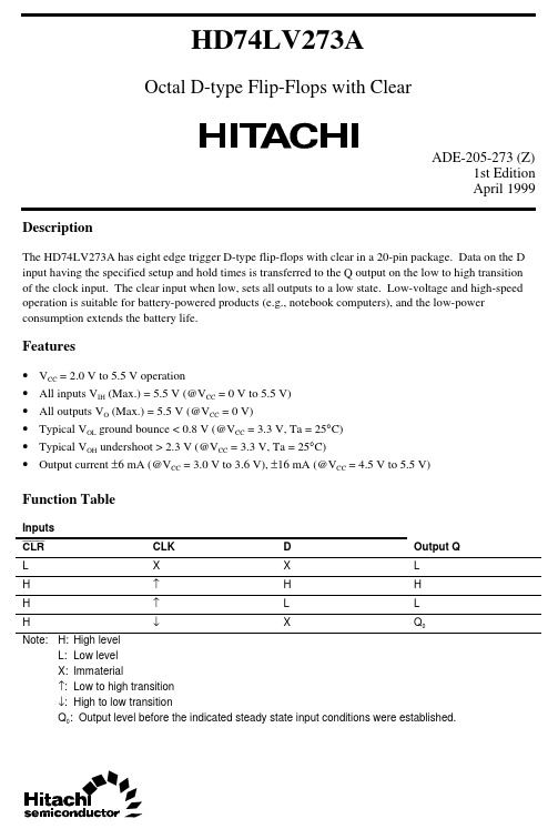
Q CLR
D CK
Q CLR
CK D
16 VCC 15 6Q 14 6D
D CK CLR
Q
CK D CLR
Q
13 5D 12 5Q
D CK CLR
Q
CK D CLR
Q
11 4D 10 4Q
9 Clock
(Top view)
Clock 1D
Clear 2D
3D
4D
5D
6D
CK
Q
1Q
D CL
CK Q
3. Hitachi makes every attempt to ensure that its products are of high quality and reliability. However, contact Hitachi’s sales office before using the product in an application that demands especially high quality and reliability or where its failure or malfunction may directly threaten human life or cause risk of bodily injury, such as aerospace, aeronautics, nuclear power, combustion control, transportation, traffic, safety equipment or medical equipment for life support.
Unit: mm
7.80
+ –
74HC27D中文资料

December 1990
3
元器件交易网
Philips Semiconductors
Triple 3-input NOR gate
Product specification
74HC/HCT27
DC CHARACTERISTICS FOR 74HC
For the DC characteristics see “74HC/HCT/HCU/HCMOS Logic Family Specifications”.
74HC/HCT27 Triple 3-input NOR gate
Product specification File under Integrated Circuits, IC06
December 1990
元器件交易网
Philips Semiconductors
Triple 3-input NOR gate
NAME AND FUNCTION data inputs data inputs data inputs ground (0 V) data outputs positive supply voltage
Product specification
74HC/HCT27
Fig.1 Pin configuration. Fig.4 Functional diagram.
+25
−40 to +85
−40 to +125
UNIT
VCC (V)
WAVEFORMS
min. typ. max. min. max. min. max.
tPHL/ tPLH propagation delay nA, nB, nC to nY
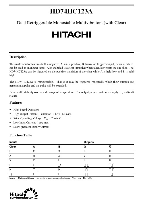
HD74HC123中文资料
DP-16 Conforms Conforms 1.07 g
元器件交易网
10.06
10.5 Max
16
9
5.5
1
8
0.80 Max
2.20 Max
0.10 ± 0.10
1.27
*0.42 ± 0.08 0.40 ± 0.06
0.15 0.12 M
*Dimension including the plating thickness Base material dimension
Output rise time tTLH
2.0
— — 75 — 95 ns
4.5
— 5 15 — 19
6.0
— — 13 — 16
Output fall time tTHL
2.0
— — 75 — 95 ns
4.5
— 5 15 — 19
6.0
— — 13 — 16
Pulse width
tw
2.0
150 — — 190 — ns A, B, Clear
VCC (V) 2.0 4.5
Min Typ Max Min — — 210 — — 22 42 —
Max Unit 265 ns 53
Test Conditions A, B or Clear to Q
6.0
— — 36 — 45
t PHL
2.0
— — 240 — 300 ns A, B or Clear to Q
4.5
— 1.0 — — — ms Cext = 0.1 µF, Rext = 10 kΩ
—
— 5 10 — 10 pF
Caution in use: In order to prevent any malfunctions due to noise, connect a high-frequency performance
HD74HC352RP中文资料
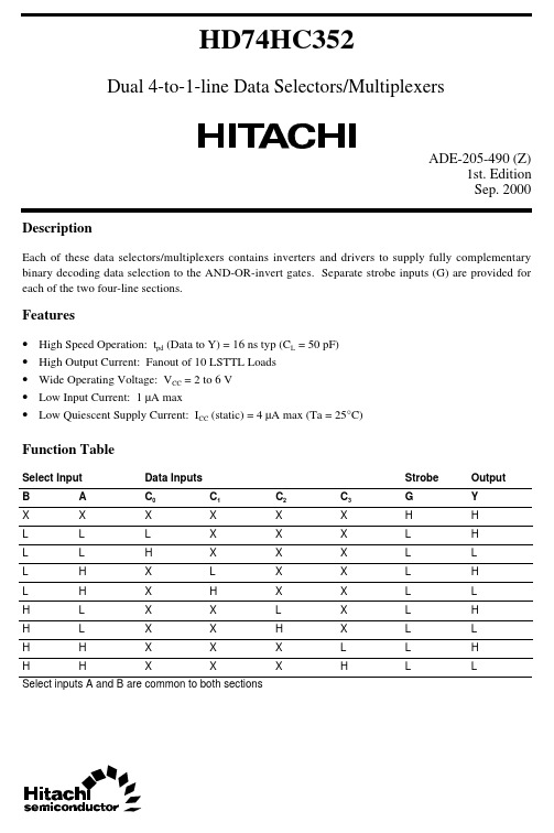
HD74HC352Dual 4-to-1-line Data Selectors/MultiplexersADE-205-490 (Z)1st. EditionSep. 2000 DescriptionEach of these data selectors/multiplexers contains inverters and drivers to supply fully complementary binary decoding data selection to the AND-OR-invert gates. Separate strobe inputs (G) are provided for each of the two four-line sections.Features• High Speed Operation: t pd (Data to Y) = 16 ns typ (C L = 50 pF)• High Output Current: Fanout of 10 LSTTL Loads• Wide Operating Voltage: V CC = 2 to 6 V• Low Input Current: 1 µA max• Low Quiescent Supply Current: I CC (static) = 4 µA max (Ta = 25°C)Function TableSelect Input Data Inputs Strobe OutputB A C0C1C2C3G YX X X X X X H H L L L X X X L H L L H X X X L L L H X L X X L H L H X H X X L L H L X X L X L H H L X X H X L L H H X X X L L H H H X X X H L L Select inputs A and B are common to both sectionsHD74HC352 Pin Arrangement2HD74HC352 Logic Diagram3HD74HC3524DC CharacteristicsTa = 25°CTa = –40 to +85°CItem Symbol V CC (V)Min Typ Max MinMax Unit Test ConditionsInput voltageV IH2.0 1.5—— 1.5—V4.5 3.15—— 3.15—6.04.2—— 4.2—V IL2.0——0.5—0.5V 4.5—— 1.35—1.356.0——1.8— 1.8Output voltageV OH2.0 1.9 2.0— 1.9—VVin = V IH or V IL I OH = –20 µA4.5 4.4 4.5— 4.4—6.05.96.0— 5.9—4.5 4.18—— 4.13—I OH = –4 mA 6.05.68——5.63—I OH = –5.2 mAV OL2.0—0.00.1—0.1VVin = V IH or V IL I OL = 20 µA4.5—0.00.1—0.16.0—0.00.1—0.14.5——0.26—0.33I OL = 4 mA 6.0——0.26—0.33I OL = 5.2 mAInput current Iin 6.0——±0.1—±1.0µA Vin = V CC or GNDQuiescent supply currentI CC6.0——4.0—40µAVin = V CC or GND, Iout = 0 µAHD74HC3525AC Characteristics (C L = 50 pF, Input t r = t f = 6 ns)Ta = 25°CTa = –40 to +85°CItem Symbol V CC (V)Min Typ Max MinMax Unit Test Conditions Propagation delay t PLH2.0——125—155nsData to Ytimet PHL4.5—1625—316.0——21—262.0——160—200nsA orB to Y4.5—1832—406.0——27—342.0——100—125nsG to Y4.5—1020—256.0——17—21Output rise/fall t TLH 2.0——75—95ns timet THL 4.5—515—196.0——13—16Input capacitanceCin——510—10pFHD74HC352 Package Dimensions6HD74HC3527HD74HC3528Cautions1.Hitachi neither warrants nor grants licenses of any rights of Hitachi’s or any third party’s patent,copyright, trademark, or other intellectual property rights for information contained in this document.Hitachi bears no responsibility for problems that may arise with third party’s rights, includingintellectual property rights, in connection with use of the information contained in this document.2.Products and product specifications may be subject to change without notice. Confirm that you have received the latest product standards or specifications before final design, purchase or use.3.Hitachi makes every attempt to ensure that its products are of high quality and reliability. However,contact Hitachi’s sales office before using the product in an application that demands especially high quality and reliability or where its failure or malfunction may directly threaten human life or cause risk of bodily injury, such as aerospace, aeronautics, nuclear power, combustion control, transportation,traffic, safety equipment or medical equipment for life support.4.Design your application so that the product is used within the ranges guaranteed by Hitachi particularly for maximum rating, operating supply voltage range, heat radiation characteristics, installationconditions and other characteristics. Hitachi bears no responsibility for failure or damage when used beyond the guaranteed ranges. Even within the guaranteed ranges, consider normally foreseeable failure rates or failure modes in semiconductor devices and employ systemic measures such as fail-safes, so that the equipment incorporating Hitachi product does not cause bodily injury, fire or other consequential damage due to operation of the Hitachi product.5.This product is not designed to be radiation resistant.6.No one is permitted to reproduce or duplicate, in any form, the whole or part of this document without written approval from Hitachi.7.Contact Hitachi’s sales office for any questions regarding this document or Hitachi semiconductor products.Hitachi, Ltd.Semiconductor & Integrated Circuits.Nippon Bldg., 2-6-2, Ohte-machi, Chiyoda-ku, Tokyo 100-0004, Japan Tel: Tokyo (03) 3270-2111 Fax: (03) 3270-5109Copyright © Hitachi, Ltd., 2000. All rights reserved. Printed in Japan.Hitachi Asia Ltd. Hitachi Tower16 Collyer Quay #20-00, Singapore 049318Tel : <65>-538-6533/538-8577 Fax : <65>-538-6933/538-3877URL : .sg URLNorthAmerica : /Europe : /hel/ecg Asia : Japan : http://www.hitachi.co.jp/Sicd/indx.htmHitachi Asia Ltd.(Taipei Branch Office)4/F, No. 167, Tun Hwa North Road, Hung-Kuo Building, Taipei (105), Taiwan Tel : <886>-(2)-2718-3666 Fax : <886>-(2)-2718-8180 Telex : 23222 HAS-TPURL : Hitachi Asia (Hong Kong) Ltd. Group III (Electronic Components) 7/F., North Tower, World Finance Centre,Harbour City, Canton Road Tsim Sha Tsui, Kowloon, Hong KongTel : <852>-(2)-735-9218 Fax : <852>-(2)-730-0281URL : Hitachi Europe Ltd.Electronic Components Group.Whitebrook ParkLower Cookham Road MaidenheadBerkshire SL6 8YA, United Kingdom Tel: <44> (1628) 585000Fax: <44> (1628) 585160Hitachi Europe GmbHElectronic Components Group Dornacher Stra βe 3D-85622 Feldkirchen, Munich GermanyTel: <49> (89) 9 9180-0Fax: <49> (89) 9 29 30 00Hitachi Semiconductor (America) Inc.179 East Tasman Drive,San Jose,CA 95134 Tel: <1> (408) 433-1990Fax: <1>(408) 433-0223For further information write to:Colophon 2.0。
HD74HC292P中文资料

HD74HC292/HD74HC294Programmable Frequency Divider/Digital TimerDescriptionThis device divides the incoming clock frequency by a number (a power of 2) that is preset by the Programming inputs. It has two Clock inputs, either of which may be used as a clock inhibit. The device also has an active-low Reset, which initializes the internal flip-flop states. Test Point outputs (TP1, TP2, TP3) are provided with HD74HC292 to facilitate incoming inspections.Test Point output is provided with HD74HC294 to facilitate incoming inspections.Features• High Speed Operation: t pd (Clock to Q) = 16 ns typ (C L = 50 pF)• High Output Current: Fanout of 10 LSTTL Loads• Wide Operating Voltage: V CC = 2 to 6 V• Low Input Current: 1 µA max• Low Quiescent Supply Current: I CC (static) = 4 µA max (Ta = 25°C)Function TableCLR CLK1CLK2Q Output ModeL X X Cleared to LH H X InhibitH X H InhibitHD74HC292/HD74HC294HD74HC292ProgrammingInputs Frequency DivisionQ Out TP1TP2TP3E D C B A Binary Decimal Binary Decimal Binary Decimal Binary DecimalL L L L L Inhibit Inhibit Inhibit Inhibit Inhibit Inhibit Inhibit Inhibit L L L L H Inhibit Inhibit Inhibit Inhibit Inhibit Inhibit Inhibit Inhibit L L L H L22429512217131,07222416,777,216 L L L H H23829512217131,07222416,777,216 L L H L L241629512217131,07222416,777,216 L L H L H253229512217131,07222416,777,216 L L H H L266429512217131,07222416,777,216 L L H H H2712829512217131,07222416,777,216 L H L L L2825629512217131,072224 L H L L H2951229512217131,072224 L H L H L2101,02429512217131,0722416 L H L H H2112,04829512217131,0722416 L H H L L2124,09629512217131,0722664 L H H L H2138,19229512217131,0722664 L H H H L21416,38429512Disabled LOW28256 L H H H H21532,76829512Disabled LOW28256 H L L L L21665,536295122382101,024 H L L L H217131,072295122382101,024 H L L H L218262,1442951225322124,096 H L L H H219524,2882951225322124,096 H L H L L2201,048,576295122712821416,384 H L H L H2212,097,152295122712821416,384 H L H H L2224,194,304Disabled LOW2951221665,536 H L H H H2238,388,608Disabled LOW2951221665,536 H H L L L22416,777,2162382112,048218262,144 H H L L H22533,554,4322382112,048218262,144 H H L H L22667,108,86425322138,1922201,048,576 H H L H H227134,217,72825322138,1922201,048,576 H H H L L228268,435,4562712821532,7682224,194,304 H H H L H229536,870,9122712821532,7682224,194,304 H H H H L2301,073,741,82429512217131,07222416,777,216 H H H H H2312,147,483,64829512217131,07222416,777,2162HD74HC292/HD74HC294HD74HC294Programming Inputs Frequency DivisionQ Output TP OutputD C B A Binary Decimal Binary DecimalL L L L Inhibit Inhibit Inhibit Inhibit L L L H Inhibit Inhibit Inhibit Inhibit L L H L22429512 L L H H23829512 L H L L241629512 L H L H253229512 L H H L266429512 L H H H27128Disabled LOW H L L L28256224 H L L H29512238 H L H L2101,0242416 H L H H2112,0482532 H H L L2124,0962664 H H L H2138,19227128 H H H L21416,38428256 H H H H21532,768295123HD74HC292/HD74HC294 Pin ArrangementHD74HC292HD74HC2944HD74HC292/HD74HC294 Logic DiagramHD74HC2925HD74HC292/HD74HC294 HD74HC2946HD74HC292/HD74HC2947DC CharacteristicsTa = 25°CTa = –40 to +85°CItem Symbol V CC (V)Min Typ Max MinMax Unit Test ConditionsInput voltageV IH2.0 1.5—— 1.5—V4.5 3.15—— 3.15—6.04.2—— 4.2—V IL2.0——0.5—0.5V 4.5—— 1.35—1.356.0——1.8— 1.8Output voltageV OH2.0 1.9 2.0— 1.9—VVin = V IH or V IL I OH = –20 µA4.5 4.4 4.5— 4.4—6.05.96.0— 5.9—4.5 4.18—— 4.13—I OH = –4 mA 6.05.68——5.63—I OH = –5.2 mAV OL2.0—0.00.1—0.1VVin = V IH or V IL I OL = 20 µA4.5—0.00.1—0.16.0—0.00.1—0.14.5——0.26—0.33I OL = 4 mA 6.0——0.26—0.33I OL = 5.2 mAInput current Iin 6.0——±0.1—±1.0µA Vin = V CC or GNDQuiescent supply currentI CC6.0——4.0—40µAVin = V CC or GND, Iout = 0 µAHD74HC292/HD74HC2948AC Characteristics (C L = 50 pF, Input t r = t f = 6 ns)Ta = 25°CTa = –40 to +85°CItemSymbol V CC (V)Min Typ Max MinMax Unit Test ConditionsMaximum clock f max2.0——5—4MHzfrequency4.5——27—216.0——31—24Propagation delay t PLH 2.0——600—750nsClock to outputtime4.5—16120—1506.0——100—125Removal timet rem2.0100——125—ns 4.520–4—25—6.017——21—Pulse widtht w2.080——100—ns 4.51614—20—6.014–—17—Output rise/fall t TLH 2.0——75—95ns timet THL 4.5—515—196.0——13—16Input capacitanceCin——510—10pFHitachi CodeJEDECEIAJWeight (reference value)DP-16 Conforms Conforms 1.07 gHitachi Code JEDEC EIAJWeight (reference value)FP-16DA —Conforms 0.24 g*Dimension including the plating thicknessBase material dimension° – 8°Hitachi CodeJEDECEIAJWeight (reference value)FP-16DNConformsConforms0.15 gUnit: mm*Dimension including the plating thickness Base material dimension° – 8°元器件交易网Cautions1.Hitachi neither warrants nor grants licenses of any rights of Hitachi’s or any third party’s patent,copyright, trademark, or other intellectual property rights for information contained in this document.Hitachi bears no responsibility for problems that may arise with third party’s rights, includingintellectual property rights, in connection with use of the information contained in this document.2.Products and product specifications may be subject to change without notice. Confirm that you have received the latest product standards or specifications before final design, purchase or use.3.Hitachi makes every attempt to ensure that its products are of high quality and reliability. However,contact Hitachi’s sales office before using the product in an application that demands especially high quality and reliability or where its failure or malfunction may directly threaten human life or cause risk of bodily injury, such as aerospace, aeronautics, nuclear power, combustion control, transportation,traffic, safety equipment or medical equipment for life support.4.Design your application so that the product is used within the ranges guaranteed by Hitachi particularly for maximum rating, operating supply voltage range, heat radiation characteristics, installationconditions and other characteristics. Hitachi bears no responsibility for failure or damage when used beyond the guaranteed ranges. Even within the guaranteed ranges, consider normally foreseeable failure rates or failure modes in semiconductor devices and employ systemic measures such as fail-safes, so that the equipment incorporating Hitachi product does not cause bodily injury, fire or other consequential damage due to operation of the Hitachi product.5.This product is not designed to be radiation resistant.6.No one is permitted to reproduce or duplicate, in any form, the whole or part of this document without written approval from Hitachi.7.Contact Hitachi’s sales office for any questions regarding this document or Hitachi semiconductor products.Hitachi, Ltd.Semiconductor & Integrated Circuits.Nippon Bldg., 2-6-2, Ohte-machi, Chiyoda-ku, Tokyo 100-0004, Japan Tel: Tokyo (03) 3270-2111 Fax: (03) 3270-5109Copyright ' Hitachi, Ltd., 1999. All rights reserved. Printed in Japan.Hitachi Asia Pte. Ltd.16 Collyer Quay #20-00Hitachi TowerSingapore 049318Tel: 535-2100Fax: 535-1533URLNorthAmerica : http:/Europe : /hel/ecg Asia (Singapore): .sg/grp3/sicd/index.htm Asia (Taiwan): /E/Product/SICD_Frame.htm Asia (HongKong): /eng/bo/grp3/index.htm Japan : http://www.hitachi.co.jp/Sicd/indx.htmHitachi Asia Ltd.Taipei Branch Office3F, Hung Kuo Building. No.167, Tun-Hwa North Road, Taipei (105)Tel: <886> (2) 2718-3666Fax: <886> (2) 2718-8180Hitachi Asia (Hong Kong) Ltd.Group III (Electronic Components)7/F., North Tower, World Finance Centre,Harbour City, Canton Road, Tsim Sha Tsui,Kowloon, Hong Kong Tel: <852> (2) 735 9218Fax: <852> (2) 730 0281 Telex: 40815 HITEC HXHitachi Europe Ltd.Electronic Components Group.Whitebrook ParkLower Cookham Road MaidenheadBerkshire SL6 8YA, United Kingdom Tel: <44> (1628) 585000Fax: <44> (1628) 778322Hitachi Europe GmbHElectronic components Group Dornacher Stra§e 3D-85622 Feldkirchen, Munich GermanyTel: <49> (89) 9 9180-0Fax: <49> (89) 9 29 30 00Hitachi Semiconductor (America) Inc.179 East Tasman Drive,San Jose,CA 95134 Tel: <1> (408) 433-1990Fax: <1>(408) 433-0223For further information write to:。
HD74LV123AFPEL资料
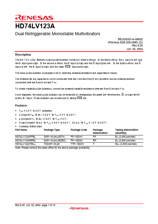
HD74LV123ADual Retriggerable Monostable MultivibratorsREJ03D0314–0600Z(Previous ADE-205-258D (Z))Rev.6.00Jun. 02, 2004 DescriptionThe HD74LV123A features output pulse-duration control by three methods. In the first method, the A input is low and the B input goes high. In the second method, the B input is high and the A input goes low. In the third method, the A input is low, the B input is high, and the clear (CLR) input goes high.The basic pulse duration is programmed by selecting external resistance and capacitance values.The external timing capacitor must be connected between Cext and Rext/Cext (positive) and an external resistor connected between Rext/Cext and VccTo obtain variable pulse durations, connect an external variable resistance between Rext/Cext and Vcc.Once triggered, the basic pulse duration can be extended by retriggering the gated low-level-active (A) or high-level-active (B) input. Pulse duration can be reduced by taking CLR low.Features•V CC = 2.0 V to 5.5 V operation•All inputs V IH (Max.) = 5.5 V (@V CC = 0 V to 5.5 V)•All outputs V O (Max.) = 5.5 V (@V CC = 0 V)•Output current ±6 mA (@V CC = 3.0 V to 3.6 V), ±12 mA (@V CC = 4.5 V to 5.5 V)•Ordering InformationPart Name Package Type Package Code PackageAbbreviation Taping Abbreviation (Quantity)HD74LV123AFPEL SOP–16 pin(JEITA)FP–16DAV FP EL (2,000 pcs/reel) HD74LV123ARPEL SOP–16 pin(JEDEC)FP–16DNV RP EL (2,500 pcs/reel) HD74LV123ATELL TSSOP–16 pin TTP–16DAV T ELL (2,000 pcs/reel) Note: Please consult the sales office for the above package availability.Function TableInputs OutputsCLR A B Q Q L X X L H H H X L HL:Low levelX:Immaterial↑:Low to high transition↓:High to low transition:High level pulse:Low level pulsePin ArrangementAbsolute Maximum RatingsItemSymbol Ratings Unit ConditionsSupply voltage range V CC –0.5 to 7.0V Input voltage range*V I –0.5 to 7.0V –0.5 to V CC + 0.5Output: H or L Output voltage range*V O–0.5 to 7.0V V CC : OFF Input clamp current I IK –20mA V I < 0Output clamp currentI OK ±50mA V O < 0 or V O > V CC Continuous output current I O±25mA V O = 0 to V CCContinuous current through V CC or GNDI CC or I GND ±50mA 785SOP Maximum power dissipation at Ta = 25°C (in still air)*3P T 500mW TSSOPStorage temperatureTstg–65 to 150°CNotes:The absolute maximum ratings are values, which must not individually be exceeded, and furthermore, no two ofwhich may be realized at the same time.1.The input and output voltage ratings may be exceeded if the input and output clamp-current ratings areobserved.2.This value is limited to 5.5 V maximum.3.The maximum package power dissipation was calculated using a junction temperature of 150°C.Recommended Operating ConditionsItemSymbol Min Typ Max Unit ConditionsSupply voltage range V CC 2.0— 5.5V Input voltage range V I 0— 5.5V Output voltage range V O 0—V CC V ——–50µA V CC = 2.0 V——–2V CC = 2.3 to 2.7 V ——–6V CC = 3.0 to 3.6 V I OH——–12mAV CC = 4.5 to 5.5 V ——50µA V CC = 2.0 V——2V CC = 2.3 to 2.7 V ——6V CC = 3.0 to 3.6 V Output currentI OL——12mAV CC = 4.5 to 5.5 V 0—200V CC = 2.3 to 2.7 V 0—100V CC = 3.0 to 3.6 V Input transition rise or fall rate ∆t /∆v 0—20ns/VV CC = 4.5 to 5.5 V 5——V CC = 2.0 V External timing resistance Rext 1——k ΩV CC ≥ 2.3 VExternal timing capacitance Cext —Unlimited —F Power-up ramp rate∆t /∆V CC 1——ms/V Operating free-air temperatureTa–40—85°CNote:Unused or floating inputs must be held high or low.Logic DiagramDC Electrical CharacteristicsTa = –40 to 85°CItem Symbol V CC (V)*Min Typ Max Unit Test Conditions2.01.5——2.3 to 2.7V CC × 0.7——3.0 to 3.6V CC × 0.7——V IH4.5 to5.5V CC × 0.7——2.0——0.52.3 to 2.7——V CC × 0.33.0 to 3.6——V CC × 0.3Input voltageV IL4.5 to5.5——V CC × 0.3VMin to Max V CC – 0.1——I OH = –50 µA 2.3 2.0——I OH = –2 mA 3.0 2.48——I OH = –6 mA V OH 4.53.8——I OH = –12 mA Min to Max ——0.1I OL = 50 µA 2.3——0.4I OL = 2 mA 3.0——0.44I OL = 6 mA Output voltage V OL4.5——0.55VI OL = 12 mAInput current I IN 0 to 5.5——±1µA V IN = 5.5 V or GND Input current Rext / Cext I IN 5.5——±2.5µA V IN = V CC or GND Quiescent supply currentI CC 5.5——20µA V IN = V CC or GND, I O = 02.3——2203.0——2804.5——650Active state supply current (per circuit)∆I CC5.5——975µAV IN = V CC or GND Rext/Cext = 0.5 V CCOutput leakage currentI OFF 0——5µA V I or V O = 0 V to 5.5 V Input capacitanceC IN3.3—4.0—pFV I = V CC or GNDNote:For conditions shown as Min or Max, use the appropriate values under recommended operating conditions.Switching CharacteristicsV CC = 2.5 ± 0.2 VTa = 25°CTa = –40 to 85°C Item Symbol Min Typ Max Min Max Unit TestConditionsFROM (Input)TO(Output)—13.531.4 1.037.0C L = 15 pF —16.036.0 1.042.0C L = 50 pF A or B Q or Q —11.025.0 1.029.5C L = 15 pF —13.032.8 1.034.5C L = 50 pF —14.033.4 1.039.0C L = 15 pF Propagation delay timet PLH t PHL—16.038.0 1.044.0nsC L = 50 pFCLR (Trigger)Q or Q—170260—320ns C L = 50 pF, Cext = 28 pF, Rext = 2 k Ω9010011090110µs C L = 50 pF,Cext = 0.01 µF, Rext = 10 k Ωt wQ0.91.0 1.10.9 1.1ms C L = 50 pF,Cext = 0.1 µF, Rext = 10 k ΩOutput pulse width∆t wQ —±1———%C L = 50 pF Pulse width t w 6.0—— 6.5—ns A , B or CLR—40———ns A , or B(Rext = 1 k Ω, Cext = 100 pF)Retrigger timet rr—1.5———µsA , or B(Rext = 1 k Ω, Cext = 0.01 µF)V CC = 3.3 ± 0.3 VTa = 25°CTa = –40 to 85°C Item Symbol Min Typ Max Min Max Unit TestConditions FROM (Input)TO(Output)—9.720.6 1.024.0C L = 15 pF —11.524.1 1.027.5C L = 50 pF A or B Q or Q —8.015.8 1.018.5C L = 15 pF —9.519.3 1.022.0C L = 50 pF CLR Q or Q —9.922.4 1.026.0C L = 15 pF Propagation delay timet PLH t PHL—11.525.9 1.029.5nsC L = 50 pF(Trigger)Q or Q—150240—300ns C L = 50 pF, Cext = 28 pF, Rext = 2 k Ω9010011090110µs C L = 50 pF,Cext = 0.01 µF, Rext = 10 k Ωt wQ0.91.0 1.10.9 1.1ms C L = 50 pF,Cext = 0.1 µF, Rext = 10 k ΩOutput pulse width∆t wQ —±1———%C L = 50 pF Pulse width t w 5.0—— 5.0—ns A , B or CLR—30———ns A , or B(Rext = 1 k Ω, Cext = 100 pF)Retrigger timet rr—1.2———µsA , or B(Rext = 1 k Ω, Cext = 0.01 µF)Switching Characteristics (cont)V CC = 5.0 ± 0.5 VTa = 25°CTa = –40 to 85°C Item Symbol Min Typ Max Min Max Unit TestConditionsFROM (Input)TO(Output)—7.312.0 1.014.0C L = 15 pF —8.514.0 1.016.0C L = 50 pF A or B Q or Q — 5.99.4 1.011.0C L = 15 pF —7.511.4 1.013.0C L = 50 pF —7.312.9 1.015.0C L = 15 pF Propagation delay timet PLH t PHL—8.714.9 1.017.0nsC L = 50 pFCLR (Trigger)Q or Q—140200—240ns C L = 50 pF, Cext = 28 pF, Rext = 2 k Ω9010011090110µs C L = 50 pF,Cext = 0.01 µF, Rext = 10 k Ωt wQ0.91.0 1.10.9 1.1ms C L = 50 pF,Cext = 0.1 µF, Rext = 10 k ΩOutput pulse width∆t wQ —±1———%C L = 50 pF Pulse width t w 5.0—— 5.0—ns A , B or CLR—20———ns A , or B(Rext = 1 k Ω, Cext = 100 pF)Retrigger timet rr—0.95———µsA , or B(Rext = 1 k Ω, Cext = 0.01 µF)Operating CharacteristicsC L = 50 pFTa = 25°CItemSymbol V CC (V)Min Typ Max Unit Test Conditions 3.3—74.0—Power dissipation capacitanceC PD5.0—86.0—pFf = 10 MHzTest CircuitTiming diagramApplication DataPackage Dimensions RENESAS SALES OFFICESRenesas Technology America, Inc.450 Holger Way, San Jose, CA 95134-1368, U.S.ATel: <1> (408) 382-7500 Fax: <1> (408) 382-7501Renesas Technology Europe Limited.Dukes Meadow, Millboard Road, Bourne End, Buckinghamshire, SL8 5FH, United KingdomTel: <44> (1628) 585 100, Fax: <44> (1628) 585 900Renesas Technology Europe GmbHDornacher Str. 3, D-85622 Feldkirchen, GermanyTel: <49> (89) 380 70 0, Fax: <49> (89) 929 30 11Renesas Technology Hong Kong Ltd.7/F., North Tower, World Finance Centre, Harbour City, Canton Road, Hong KongTel: <852> 2265-6688, Fax: <852> 2375-6836Renesas Technology Taiwan Co., Ltd.FL 10, #99, Fu-Hsing N. Rd., Taipei, TaiwanTel: <886> (2) 2715-2888, Fax: <886> (2) 2713-2999Renesas Technology (Shanghai) Co., Ltd.26/F., Ruijin Building, No.205 Maoming Road (S), Shanghai 200020, ChinaTel: <86> (21) 6472-1001, Fax: <86> (21) 6415-2952Renesas Technology Singapore Pte. Ltd.1, Harbour Front Avenue, #06-10, Keppel Bay Tower, Singapore 098632Tel: <65> 6213-0200, Fax: <65> 6278-8001Colophon .1.0。
HD74AC273P中文资料

HD74AC273Octal D-Type Flip-FlopADE-205-386 (Z)1st. EditionSep. 2000 DescriptionThe HD74AC273 has eight edge-triggered D-type flip-flops with individual D inputs and Q outputs. The common buffered Clock (CP) and Master Reset (MR) inputs load and reset (clear) all flip-flops simultaneously.The register is fully edge-triggered. The state of each D input, one setup time before the Low-to-High clock transition, is transferred to the corresponding flip-flops’s Q outputAll outputs will be forced Low independently of Clock or Data inputs by a Low voltage level on the MR input. The device is useful for applications where the true output only is required and the Clock and Master Reset are common to all storage elements.Features• Ideal Buffer for MOS Microprocessor or Memory• Eight Edge-Triggered D Flip-Flops• Buffered Common Clock• Buffered, Asynchronous Master Reset• See HD74AC373 for Transparent Latch Version• See HD74AC374 for 3-State Version• Outputs Source/Sink 24 mAHD74AC2732Pin ArrangementLogic SymbolPin NamesD 0 – D 7Data Inputs MR Master Reset CP Clock Pulse Input Q 0 – Q 7Data OutputsHD74AC2733Logic DiagramMode Select-Truth TableInputsOutputs Operating Mode MR CP D n Q n Reset (Clear)L XX L L :Low Voltage Level X :Immaterial:Low-to-High Clock TransitionDC Characteristics (unless otherwise specified)ItemSymbol Max Unit ConditionMaximum quiescent supply current I CC 80µA V IN = V CC or ground, V CC = 5.5 V,Ta = Worst caseMaximum quiescent supply currentI CC8.0µAV IN = V CC or ground, V CC = 5.5 V,Ta = 25°CHD74AC2734AC Characteristics: HD74AC273Ta = +25°C C L = 50 pFTa = –40°C to +85°C C L = 50 pF ItemSymbol V CC (V)*1Min Typ Max Min Max Unit Maximum clock f max3.390125—75—MHzfrequency 5.0140175—125—Propagation delay t PLH 3.3 1.07.012.5 1.014.0ns Clock to output 5.0 1.0 5.59.0 1.010.0Propagation delay t PHL 3.3 1.07.013.0 1.014.5ns Clock to output 5.0 1.0 5.010.0 1.011.0Propagation delay t PHL 3.3 1.07.013.0 1.014.0ns MR to output 5.01.05.010.01.010.5Note:1.Voltage Range 3.3 is 3.3 V ± 0.3 VVoltage Range 5.0 is 5.0 V ± 0.5 VAC Operating Requirements: HD74AC273Ta = +25°C C L = 50 pFTa = –40°C to +85°C C L = 50 pFItemSymbol V CC (V)*1Typ Guaranteed MinimumUnit Setup time, HIGH or LOW t su3.3 3.5 5.5 6.0nsData to CP5.0 2.5 4.0 4.5Hold time, HIGH or LOW t h3.3–2.00.00.0ns Data to CP 5.0–1.0 1.0 1.0Clock pulse width t w 3.3 3.5 5.5 6.0ns HIGH or LOW 5.0 2.54.0 4.5MR Pulse width t w 3.3 2.05.56.0ns HIGH or LOW 5.0 1.5 4.0 4.5Recovery time t rec 3.3 1.5 3.5 4.5ns MR to CP 5.01.02.03.0Note:1.Voltage Range 3.3 is 3.3 V ± 0.3 VVoltage Range 5.0 is 5.0 V ± 0.5 VHD74AC2735CapacitanceItemSymbol Typ Unit Condition Input capacitanceC IN 4.5pF V CC = 5.5 V Power dissipation capacitanceC PD50.0pFV CC = 5.0 VHD74AC273 Package Dimensions6HD74AC2737HD74AC2738Cautions1.Hitachi neither warrants nor grants licenses of any rights of Hitachi’s or any third party’s patent,copyright, trademark, or other intellectual property rights for information contained in this document.Hitachi bears no responsibility for problems that may arise with third party’s rights, includingintellectual property rights, in connection with use of the information contained in this document.2.Products and product specifications may be subject to change without notice. Confirm that you have received the latest product standards or specifications before final design, purchase or use.3.Hitachi makes every attempt to ensure that its products are of high quality and reliability. However,contact Hitachi’s sales office before using the product in an application that demands especially high quality and reliability or where its failure or malfunction may directly threaten human life or cause risk of bodily injury, such as aerospace, aeronautics, nuclear power, combustion control, transportation,traffic, safety equipment or medical equipment for life support.4.Design your application so that the product is used within the ranges guaranteed by Hitachi particularly for maximum rating, operating supply voltage range, heat radiation characteristics, installationconditions and other characteristics. Hitachi bears no responsibility for failure or damage when used beyond the guaranteed ranges. Even within the guaranteed ranges, consider normally foreseeable failure rates or failure modes in semiconductor devices and employ systemic measures such as fail-safes, so that the equipment incorporating Hitachi product does not cause bodily injury, fire or other consequential damage due to operation of the Hitachi product.5.This product is not designed to be radiation resistant.6.No one is permitted to reproduce or duplicate, in any form, the whole or part of this document without written approval from Hitachi.7.Contact Hitachi’s sales office for any questions regarding this document or Hitachi semiconductor products.Hitachi, Ltd.Semiconductor & Integrated Circuits.Nippon Bldg., 2-6-2, Ohte-machi, Chiyoda-ku, Tokyo 100-0004, Japan Tel: Tokyo (03) 3270-2111 Fax: (03) 3270-5109Copyright © Hitachi, Ltd., 2000. All rights reserved. Printed in Japan.Hitachi Asia Ltd. Hitachi Tower16 Collyer Quay #20-00, Singapore 049318Tel : <65>-538-6533/538-8577 Fax : <65>-538-6933/538-3877URL : .sg URLNorthAmerica : /Europe : /hel/ecg Asia : Japan : http://www.hitachi.co.jp/Sicd/indx.htmHitachi Asia Ltd.(Taipei Branch Office)4/F, No. 167, Tun Hwa North Road, Hung-Kuo Building, Taipei (105), Taiwan Tel : <886>-(2)-2718-3666 Fax : <886>-(2)-2718-8180 Telex : 23222 HAS-TPURL : Hitachi Asia (Hong Kong) Ltd. Group III (Electronic Components) 7/F., North Tower, World Finance Centre,Harbour City, Canton Road Tsim Sha Tsui, Kowloon, Hong KongTel : <852>-(2)-735-9218 Fax : <852>-(2)-730-0281URL : Hitachi Europe Ltd.Electronic Components Group.Whitebrook ParkLower Cookham Road MaidenheadBerkshire SL6 8YA, United Kingdom Tel: <44> (1628) 585000Fax: <44> (1628) 585160Hitachi Europe GmbHElectronic Components Group Dornacher Stra βe 3D-85622 Feldkirchen, Munich GermanyTel: <49> (89) 9 9180-0Fax: <49> (89) 9 29 30 00Hitachi Semiconductor (America) Inc.179 East Tasman Drive,San Jose,CA 95134 Tel: <1> (408) 433-1990Fax: <1>(408) 433-0223For further information write to:Colophon 2.0。
74系列功能大全(中文)

74HC157 QUAD 2-INPUT MUX 四个双端多路器
ቤተ መጻሕፍቲ ባይዱ74HC161 BINARY COUNTER 二进制计数器
74HC163 DECADE COUNTERS 十进制计数器
74HC164 SERIAL-PARALLEL SHIFT REG 串入并出
7404 HEX INVERTING GATES 反向器
7406 HEX INVERTING GATES HV 高输出反向器
7408 QUAD 2-INPUT AND GATE 与门
7409 QUAD 2-INPUT AND GATES OC 与门
7410 TRIPLE 3-INPUT NAND GATES 与非门
7420 DUAL 4-INPUT NAND GATES 双四输入与非门
7426 QUAD 2-INPUT NAND GATES 与非门
7427 TRIPLE 3-INPUT NOR GATES 三输入或非门
7430 8-INPUT NAND GATES 八输入端与非门
7432 QUAD 2-INPUT OR GATES 二输入或门
7485 4-BIT MAGNITUDE COMPARATOR 四位比较器
7486 2-INPUT EXCLUSIVE OR GATES 双端异或门
74HC00 QUAD 2-INPUT NAND GATES 双输入与非门
74HC02 QUAD 2-INPUT NOR GATES 双输入或非门
74HC195 4BIT PARALLEL SHIFT 4位并行移位寄存器
74HC20 QUAD 4-INPUT NAND GATE 四个四入与非门
HD74ACT374RP中文资料

Setup time, HIGH or LOW
t su
3.3
2.0
Dn to CP
5.0
1.0
Hold time, HIGH or LOW
th
3.3
–1.0
Dn to CP
5.0
–4.0
CP pulse width, HIGH or LOW tw
3.3
4.0
5.0
2.5
Note: 1. Voltage Range 3.3 is 3.3 V ± 0.3 V Voltage Range 5.0 is 5.0 V ± 0.5 V
5.0
0.0
CP pulse width, HIGH or LOW tw
5.0
2.0
Note: 1. Voltage Range 5.0 is 5.0 V ± 0.5 V
Ta = –40°C to +85°C CL = 50 pF
Guar5
1.5
7.0
5.0
Max — — 13.5 9.5 12.5 9.0 11.5 8.5 11.5 8.5 12.5 11.0 11.5 8.5
Ta = –40°C to +85°C CL = 50 pF
Min
Max
60
—
100
—
1.0
15.5
1.0
10.5
1.0
14.0
1.0
10.0
1.0
13.0
1.0
9.5
1.0
13.0
D0
D1
D2
D3
D4
D5
D6
D7
CP
CP D QQ
HD74HC21RP中文资料

HD74HC21Dual 4-input AND GatesADE-205-414 (Z)1st. EditionSep. 2000 Features• High Speed Operation: t pd = 11 ns typ (C L = 50 pF)• High Output Current: Fanout of 10 LSTTL Loads• Wide Operating Voltage: V CC = 2 to 6 V• Low Input Current: 1 µA max• Low Quiescent Supply Current: I CC (static) = 1 µA max (Ta = 25°C)Pin ArrangementHD74HC212DC CharacteristicsTa = 25°CTa = –40 to +85°CItem Symbol V CC (V)Min Typ Max MinMax Unit Test ConditionsInput voltageV IH2.0 1.5—— 1.5—V4.5 3.15—— 3.15—6.04.2—— 4.2—V IL2.0——0.5—0.5V 4.5—— 1.35—1.356.0——1.8— 1.8Output voltageV OH2.0 1.9 2.0— 1.9—VVin = V IH or V IL I OH = –20 µA4.5 4.4 4.5— 4.4—6.05.96.0— 5.9—4.5 4.18—— 4.13—I OH = –4 mA 6.05.68——5.63—I OH = –5.2 mAV OL2.0—0.00.1—0.1VVin = V IH or V IL I OL = 20 µA4.5—0.00.1—0.16.0—0.00.1—0.14.5——0.26—0.33I OL = 4 mA 6.0——0.26—0.33I OL = 5.2 mAInput current Iin 6.0——±0.1—±1.0µA Vin = V CC or GNDQuiescent supply currentI CC6.0——1.0—10µAVin = V CC or GND, Iout = 0 µAHD74HC213AC Characteristics (C L = 50 pF, Input t r = t f = 6 ns)Ta = 25°CTa = –40 to +85°CItem SymbolV CC (V)Min Typ Max MinMax Unit Test ConditionsPropagation delay t PLH2.0——100—125nstime4.5—1020—256.0——17—21t PHL 2.0——100—125ns 4.5—1220—256.0——17—21Output rise timet TLH2.0——75—95ns 4.5—515—196.0——13—16Output fall timet THL2.0——75—95ns 4.5—515—196.0——13—16Input capacitanceCin——510—10pFHD74HC21 Package Dimensions4HD74HC215HD74HC216Cautions1.Hitachi neither warrants nor grants licenses of any rights of Hitachi’s or any third party’s patent,copyright, trademark, or other intellectual property rights for information contained in this document.Hitachi bears no responsibility for problems that may arise with third party’s rights, includingintellectual property rights, in connection with use of the information contained in this document.2.Products and product specifications may be subject to change without notice. Confirm that you have received the latest product standards or specifications before final design, purchase or use.3.Hitachi makes every attempt to ensure that its products are of high quality and reliability. However,contact Hitachi’s sales office before using the product in an application that demands especially high quality and reliability or where its failure or malfunction may directly threaten human life or cause risk of bodily injury, such as aerospace, aeronautics, nuclear power, combustion control, transportation,traffic, safety equipment or medical equipment for life support.4.Design your application so that the product is used within the ranges guaranteed by Hitachi particularly for maximum rating, operating supply voltage range, heat radiation characteristics, installationconditions and other characteristics. Hitachi bears no responsibility for failure or damage when used beyond the guaranteed ranges. Even within the guaranteed ranges, consider normally foreseeable failure rates or failure modes in semiconductor devices and employ systemic measures such as fail-safes, so that the equipment incorporating Hitachi product does not cause bodily injury, fire or other consequential damage due to operation of the Hitachi product.5.This product is not designed to be radiation resistant.6.No one is permitted to reproduce or duplicate, in any form, the whole or part of this document without written approval from Hitachi.7.Contact Hitachi’s sales office for any questions regarding this document or Hitachi semiconductor products.Hitachi, Ltd.Semiconductor & Integrated Circuits.Nippon Bldg., 2-6-2, Ohte-machi, Chiyoda-ku, Tokyo 100-0004, Japan Tel: Tokyo (03) 3270-2111 Fax: (03) 3270-5109Copyright © Hitachi, Ltd., 2000. All rights reserved. Printed in Japan.Hitachi Asia Ltd. Hitachi Tower16 Collyer Quay #20-00, Singapore 049318Tel : <65>-538-6533/538-8577 Fax : <65>-538-6933/538-3877URL : .sg URLNorthAmerica : /Europe : /hel/ecg Asia : Japan : http://www.hitachi.co.jp/Sicd/indx.htmHitachi Asia Ltd.(Taipei Branch Office)4/F, No. 167, Tun Hwa North Road, Hung-Kuo Building, Taipei (105), Taiwan Tel : <886>-(2)-2718-3666 Fax : <886>-(2)-2718-8180 Telex : 23222 HAS-TPURL : Hitachi Asia (Hong Kong) Ltd. Group III (Electronic Components) 7/F., North Tower, World Finance Centre,Harbour City, Canton Road Tsim Sha Tsui, Kowloon, Hong KongTel : <852>-(2)-735-9218 Fax : <852>-(2)-730-0281URL : Hitachi Europe Ltd.Electronic Components Group.Whitebrook ParkLower Cookham Road MaidenheadBerkshire SL6 8YA, United Kingdom Tel: <44> (1628) 585000Fax: <44> (1628) 585160Hitachi Europe GmbHElectronic Components Group Dornacher Stra βe 3D-85622 Feldkirchen, Munich GermanyTel: <49> (89) 9 9180-0Fax: <49> (89) 9 29 30 00Hitachi Semiconductor (America) Inc.179 East Tasman Drive,San Jose,CA 95134 Tel: <1> (408) 433-1990Fax: <1>(408) 433-0223For further information write to:Colophon 2.0。
HD74HC00P中文资料

HD74HC00Quad. 2-input NAND GatesREJ03D0531-0200(Previous ADE-205-403)Rev.2.00Oct 06, 2005 Features• High Speed Operation: t pd = 8.5 ns typ (C L = 50 pF)• High Output Current: Fanout of 10 LSTTL Loads• Wide Operating Voltage: V CC = 2 to 6 V• Low Input Current: 1 µA max• Low Quiescent Supply Current: I CC (static) = 1 µA max (Ta = 25°C)• Ordering InformationPart Name Package TypePackage Code(Previous Code)PackageAbbreviationTaping Abbreviation(Quantity)HD74HC00P DILP-14pin PRDP0014AB-B(DP-14AV)P —HD74HC00FPEL SOP-14 pin (JEITA) PRSP0014DF-B(FP-14DAV)FP EL (2,000 pcs/reel)HD74HC00RPEL SOP-14 pin (JEDEC) PRSP0014DE-A(FP-14DNV)RP EL (2,500 pcs/reel)HD74HC00TELL TSSOP-14pin PTSP0014JA-B(TTP-14DV)T ELL(2,000pcs/reel)Note: Please consult the sales office for the above package availability.Function TableInputs OutputA B YL L HL H HH L HH H LH : High levelL : Low levelPin ArrangementAbsolute Maximum RatingsItem Symbol Ratings UnitSupply voltage range V CC –0.5 to 7.0 V Input / Output voltage Vin, Vout –0.5 to V CC +0.5VInput / Output diode current I IK , I OK ±20 mAOutput current I O±25 mAV CC , GND current I CC or I GND ±50 mAPower dissipationP T 500 mWStorage temperature Tstg –65 to +150 °CNote: The absolute maximum ratings are values, which must not individually be exceeded, and furthermore, no two ofwhich may be realized at the same time.Recommended Operating ConditionsItem Symbol Ratings Unit ConditionsSupply voltage V CC 2 to 6 V Input / Output voltage V IN , V OUT 0 to V CC V Operating temperature Ta –40 to 85 °C 0 to 1000 V CC = 2.0 V 0 to 500V CC = 4.5 V Input rise / fall time *1t r , t f0 to 400nsV CC = 6.0 VNote: 1. This item guarantees maximum limit when one input switches. Waveform: Refer to test circuit of switching characteristics.Electrical CharacteristicsTa = 25°CTa = –40 to+85°CItem Symbol V CC (V) Min Typ Max Min Max UnitTest Conditions2.0 1.5 — — 1.5 — 4.53.15 — — 3.15 —V IH 6.0 4.2 — — 4.2 —V2.0 — — 0.5 — 0.5 4.5 — — 1.35 — 1.35Input voltage V IL6.0 — — 1.8 — 1.8 V 2.0 1.9 2.0 — 1.9 — 4.5 4.4 4.5 — 4.4 — 6.0 5.9 6.0 — 5.9 — I OH = –20 µA 4.5 4.18 — — 4.13 — I OH = –4 mA V OH6.0 5.68 — — 5.63 —V Vin = V IH or V IL I OH = –5.2 mA2.0 — 0.0 0.1 — 0.1 4.5 — 0.0 0.1 — 0.1 6.0 — 0.0 0.1 — 0.1 I OL = 20 µA 4.5 — — 0.26 — 0.33I OL = 4 mAOutput voltage V OL6.0 — — 0.26 — 0.33 V Vin = V IH or V IL I OL = 5.2 mA Input current Iin6.0 — — ±0.1 — ±1.0 µA Vin = V CC or GNDQuiescent supplycurrent I CC 6.0 — — 1.0 — 10 µA Vin = V CC or GND, Iout = 0 µASwitching Characteristics (C L = 50 pF, Input t r = t f = 6 ns)Ta = 25°CTa = –40 to +85°CItem Symbol V CC (V) Min Typ Max MinMax UnitTest Conditions2.0 — — 90 — 115 4.5 — 9 18 —23 t PLH 6.0 — — 15 —20 ns 2.0 — — 90 —115 4.5 — 8 18 — 23 Propagation delay time t PHL 6.0 — — 15 —20ns 2.0 — — 75 —95 4.5 — 7 15 — 19 Output rise time t TLH 6.0 — — 13 —16ns 2.0 — — 75 —95 4.5 — 7 15 — 19 Output fall time t THL 6.0 — — 13 —16 ns Input capacitance Cin — — 5 10 — 10 pFTest CircuitWaveformsPackage Dimensions RENESAS SALES OFFICESRefer to "/en/network" for the latest and detailed information.Renesas Technology America, Inc.450 Holger Way, San Jose, CA 95134-1368, U.S.ATel: <1> (408) 382-7500, Fax: <1> (408) 382-7501Renesas Technology Europe LimitedDukes Meadow, Millboard Road, Bourne End, Buckinghamshire, SL8 5FH, U.K.Tel: <44> (1628) 585-100, Fax: <44> (1628) 585-900Renesas Technology Hong Kong Ltd.7th Floor, North Tower, World Finance Centre, Harbour City, 1 Canton Road, Tsimshatsui, Kowloon, Hong KongTel: <852> 2265-6688, Fax: <852> 2730-6071Renesas Technology Taiwan Co., Ltd.10th Floor, No.99, Fushing North Road, Taipei, TaiwanTel: <886> (2) 2715-2888, Fax: <886> (2) 2713-2999Renesas Technology (Shanghai) Co., Ltd.Unit2607 Ruijing Building, No.205 Maoming Road (S), Shanghai 200020, ChinaTel: <86> (21) 6472-1001, Fax: <86> (21) 6415-2952Renesas Technology Singapore Pte. Ltd.1 Harbour Front Avenue, #06-10, Keppel Bay Tower, Singapore 098632Tel: <65> 6213-0200, Fax: <65> 6278-8001Renesas Technology Korea Co., Ltd.Kukje Center Bldg. 18th Fl., 191, 2-ka, Hangang-ro, Yongsan-ku, Seoul 140-702, KoreaTel: <82> 2-796-3115, Fax: <82> 2-796-2145Renesas Technology Malaysia Sdn. Bhd.Unit 906, Block B, Menara Amcorp, Amcorp Trade Centre, No.18, Jalan Persiaran Barat, 46050 Petaling Jaya, Selangor Darul Ehsan, MalaysiaTel: <603> 7955-9390, Fax: <603> 7955-9510。
74系列芯片型号与功能简介
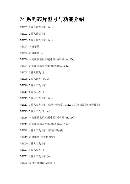
74系列芯片型号与功能介绍74HC01 2输入四与非门 (oc)74HC02 2输入四或非门74HC03 2输入四与非门 (oc)74HC04 六倒相器74HC05 六倒相器(oc)74HC06 六高压输出反相缓冲器/驱动器(oc,30v)74HC07 六高压输出缓冲器/驱动器(oc,30v)74HC08 2输入四与门74HC09 2输入四与门(oc)74HC10 3输入三与非门74HC11 3输入三与门74HC12 3输入三与非门 (oc)74HC13 4输入双与非门 (斯密特触发) 74HC14 六倒相器(斯密特触发) 74HC15 3输入三与门 (oc)74HC16 六高压输出反相缓冲器/驱动器(oc,15v)74HC17 六高压输出缓冲器/驱动器(oc,15v)74HC18 4输入双与非门 (斯密特触发)74HC19 六倒相器(斯密特触发)74HC20 4输入双与非门74HC21 4输入双与门74HC22 4输入双与非门(oc)74HC23 双可扩展的输入或非门74HC24 2输入四与非门(斯密特触发)74HC25 4输入双或非门(有选通)74HC26 2输入四高电平接口与非缓冲器(oc,15v) 74HC27 3输入三或非门74HC28 2输入四或非缓冲器74HC30 8输入与非门74HC31 延迟电路74HC32 2输入四或门74HC33 2输入四或非缓冲器(集电极开路输出) 74HC34 六缓冲器74HC35 六缓冲器(oc)74HC36 2输入四或非门(有选通)74HC37 2输入四与非缓冲器74HC38 2输入四或非缓冲器(集电极开路输出) 74HC39 2输入四或非缓冲器(集电极开路输出) 74HC40 4输入双与非缓冲器74HC41 bcd-十进制计数器74HC42 4线-10线译码器(bcd输入)74HC43 4线-10线译码器(余3码输入)74HC44 4线-10线译码器(余3葛莱码输入)74HC45 bcd-十进制译码器/驱动器74HC46 bcd-七段译码器/驱动器74HC47 bcd-七段译码器/驱动器74HC48 bcd-七段译码器/驱动器74HC49 bcd-七段译码器/驱动器(oc)74HC50 双二路2-2输入与或非门(一门可扩展)74HC51 双二路2-2输入与或非门74HC51 二路3-3输入,二路2-2输入与或非门74HC52 四路2-3-2-2输入与或门(可扩展)74HC53 四路2-2-2-2输入与或非门(可扩展)74HC53 四路2-2-3-2输入与或非门(可扩展)74HC54 四路2-2-2-2输入与或非门74HC54 四路2-3-3-2输入与或非门74HC54 四路2-2-3-2输入与或非门74HC55 二路4-4输入与或非门(可扩展)74HC60 双四输入与扩展74HC61 三3输入与扩展74HC62 四路2-3-3-2输入与或扩展器74HC63 六电流读出接口门74HC64 四路4-2-3-2输入与或非门74HC65 四路4-2-3-2输入与或非门(oc)74HC70 与门输入上升沿jk触发器74HC71 与输入r-s主从触发器74HC72 与门输入主从jk触发器74HC73 双j-k触发器(带清除端)74HC74 正沿触发双d型触发器(带预置端和清除端) 74HC75 4位双稳锁存器74HC76 双j-k触发器(带预置端和清除端)74HC77 4位双稳态锁存器74HC78 双j-k触发器(带预置端,公共清除端和公共时钟端) 74HC80 门控全加器74HC81 16位随机存取存储器74HC82 2位二进制全加器(快速进位)74HC83 4位二进制全加器(快速进位)74HC84 16位随机存取存储器74HC85 4位数字比较器74HC86 2输入四异或门74HC87 四位二进制原码/反码/oi单元74HC89 64位读/写存储器74HC90 十进制计数器74HC91 八位移位寄存器74HC92 12分频计数器(2分频和6分频)74HC93 4位二进制计数器74HC94 4位移位寄存器(异步)74HC157 四2选1数据选择器/多路选择器74HC158 四2选1数据选择器(反相输出)74HC160 可预置bcd计数器(异步清除)74HC161 可预置四位二进制计数器(并清除异步)74HC162 可预置bcd计数器(异步清除)74HC163 可预置四位二进制计数器(并清除异步)74HC164 8位并行输出串行移位寄存器74HC165 并行输入8位移位寄存器(补码输出)74HC167 同步十进制比率乘法器74HC168 4位加/减同步计数器(十进制) 74HC169 同步二进制可逆计数器74HC170 4*4寄存器堆74HC171 四d触发器(带清除端)74HC172 16位寄存器堆74HC173 4位d型寄存器(带清除端)74HC174 六d触发器74HC175 四d触发器74HC176 十进制可预置计数器74HC177 2-8-16进制可预置计数器74HC178 四位通用移位寄存器74HC179 四位通用移位寄存器74HC180 九位奇偶产生/校验器74HC181 算术逻辑单元/功能发生器74HC182 先行进位发生器74HC183 双保留进位全加器74HC184 bcd-二进制转换器74HC185 二进制-bcd转换器74HC190 同步可逆计数器(bcd,二进制) 74HC191 同步可逆计数器(bcd,二进制) 74HC192 同步可逆计数器(bcd,二进制) 74HC193 同步可逆计数器(bcd,二进制)74HC210 2-5-10进制计数器74HC213 2-n-10可变进制计数器74HC221 双单稳触发器74HC230 八3态总线驱动器74HC231 八3态总线反向驱动器74HC240 八缓冲器/线驱动器/线接收器(反码三态输出) 74HC241 八缓冲器/线驱动器/线接收器(原码三态输出) 74HC242 八缓冲器/线驱动器/线接收器74HC243 4同相三态总线收发器74HC244 八缓冲器/线驱动器/线接收器74HC245 八双向总线收发器74HC246 4线-七段译码/驱动器(30v)74HC247 4线-七段译码/驱动器(15v)74HC248 4线-七段译码/驱动器74HC249 4线-七段译码/驱动器74HC251 8选1数据选择器(三态输出)74HC253 双四选1数据选择器(三态输出)74HC256 双四位可寻址锁存器74HC257 四2选1数据选择器(三态输出)74HC258 四2选1数据选择器(反码三态输出)74HC259 8为可寻址锁存器74HC260 双5输入或非门74HC261 4*2并行二进制乘法器74HC265 四互补输出元件74HC266 2输入四异或非门(oc)74HC270 2048位rom (512位四字节,oc)74HC271 2048位rom (256位八字节,oc)74HC273 八d触发器74HC274 4*4并行二进制乘法器74HC275 七位片式华莱士树乘法器74HC276 四jk触发器74HC278 四位可级联优先寄存器74HC279 四s-r锁存器74HC280 9位奇数/偶数奇偶发生器/较验器74HC283 4位二进制全加器74HC290 十进制计数器74HC291 32位可编程模74HC293 4位二进制计数器74HC294 16位可编程模74HC295 四位双向通用移位寄存器74HC298 四-2输入多路转换器(带选通)74HC299 八位通用移位寄存器(三态输出)74HC348 8-3线优先编码器(三态输出)74HC352 双四选1数据选择器/多路转换器74HC353 双4-1线数据选择器(三态输出)74HC354 8输入端多路转换器/数据选择器/寄存器,三态补码输出74HC355 8输入端多路转换器/数据选择器/寄存器,三态补码输出74HC356 8输入端多路转换器/数据选择器/寄存器,三态补码输出74HC357 8输入端多路转换器/数据选择器/寄存器,三态补码输出74HC365 6总线驱动器74HC366 六反向三态缓冲器/线驱动器74HC367 六同向三态缓冲器/线驱动器74HC368 六反向三态缓冲器/线驱动器74HC373 八d锁存器74HC374 八d触发器(三态同相)74HC375 4位双稳态锁存器74HC377 带使能的八d触发器74HC378 六d触发器74HC379 四d触发器74HC381 算术逻辑单元/函数发生器74HC382 算术逻辑单元/函数发生器74HC384 8位*1位补码乘法器74HC385 四串行加法器/乘法器74HC386 2输入四异或门74HC390 双十进制计数器74HC391 双四位二进制计数器74HC395 4位通用移位寄存器74HC396 八位存储寄存器74HC398 四2输入端多路开关(双路输出)74HC399 四-2输入多路转换器(带选通)74HC422 单稳态触发器74HC423 双单稳态触发器74HC440 四3方向总线收发器,集电极开路74HC441 四3方向总线收发器,集电极开路74HC442 四3方向总线收发器,三态输出74HC443 四3方向总线收发器,三态输出74HC444 四3方向总线收发器,三态输出74HC445 bcd-十进制译码器/驱动器,三态输出74HC446 有方向控制的双总线收发器74HC448 四3方向总线收发器,三态输出74HC449 有方向控制的双总线收发器74HC465 八三态线缓冲器74HC466 八三态线反向缓冲器74HC467 八三态线缓冲器74HC468 八三态线反向缓冲器74HC490 双十进制计数器74HC540 八位三态总线缓冲器(反向)74HC541 八位三态总线缓冲器74HC589 有输入锁存的并入串出移位寄存器74HC590 带输出寄存器的8位二进制计数器74HC591 带输出寄存器的8位二进制计数器74HC592 带输出寄存器的8位二进制计数器74HC593 带输出寄存器的8位二进制计数器74HC594 带输出锁存的8位串入并出移位寄存器74HC595 8位输出锁存移位寄存器74HC596 带输出锁存的8位串入并出移位寄存器74HC597 8位输出锁存移位寄存器74HC598 带输入锁存的并入串出移位寄存器74HC599 带输出锁存的8位串入并出移位寄存器74HC604 双8位锁存器74HC605 双8位锁存器74HC606 双8位锁存器74HC607 双8位锁存器74HC620 8位三态总线发送接收器(反相)74HC621 8位总线收发器74HC622 8位总线收发器74HC623 8位总线收发器74HC640 反相总线收发器(三态输出)74HC641 同相8总线收发器,集电极开路74HC642 同相8总线收发器,集电极开路74HC643 8位三态总线发送接收器74HC644 真值反相8总线收发器,集电极开路74HC645 三态同相8总线收发器74HC646 八位总线收发器,寄存器74HC647 八位总线收发器,寄存器74HC648 八位总线收发器,寄存器74HC649 八位总线收发器,寄存器74HC651 三态反相8总线收发器74HC652 三态反相8总线收发器74HC653 反相8总线收发器,集电极开路74HC654 同相8总线收发器,集电极开路74HC668 4位同步加/减十进制计数器74HC669 带先行进位的4位同步二进制可逆计数器74HC670 4*4寄存器堆(三态)74HC671 带输出寄存的四位并入并出移位寄存器74HC672 带输出寄存的四位并入并出移位寄存器74HC673 16位并行输出存储器,16位串入串出移位寄存器74HC674 16位并行输入串行输出移位寄存器74HC681 4位并行二进制累加器74HC682 8位数值比较器(图腾柱输出)74HC683 8位数值比较器(集电极开路)74HC684 8位数值比较器(图腾柱输出)74HC685 8位数值比较器(集电极开路)74HC686 8位数值比较器(图腾柱输出)74HC687 8位数值比较器(集电极开路)74HC688 8位数字比较器(oc输出)74HC689 8位数字比较器74HC690 同步十进制计数器/寄存器(带数选,三态输出,直接清除)。
HD74LV273A中文资料
0
—
—
5
current
µA
VI or VO = 0 V to 5.5 V
Input
CIN
3.3
—
2
—
pF
VI = VCC or GND
capacitance
Note: For conditions shown as Min or Max, use the appropriate values under recommended operating conditions.
Setup time
Symbol fmax
tPHL
tPLH / tPHL tPHL tPLH / tPHL tSU
Min Typ 120 205
80 160 — 4.7
— 4.8 — 6.0 — 6.2 4.5 —
Max Min — 100
— 70 8.5 1.0
9.0 1.0 10.5 1.0 11.0 1.0 — 4.5
CL = 50 pF ns
ns ns
FROM (Iபைடு நூலகம்put)
TO (Output)
CLR
Q
CLK
Q
CLR
Q
CLK
Q
Data
CLR inactive
CLR L CLK H or L
6
HD74LV273A
Switching Characteristics (cont)
• VCC = 3.3 ± 0.3 V
Function Table
Inputs
CLR
CLK
D
Output Q
L
X
X
L
H
↑
HD74LS273P中文资料
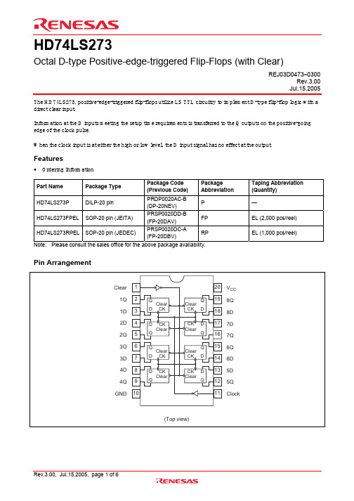
HD74LS273Octal D-type Positive-edge-triggered Flip-Flops (with Clear)REJ03D0473–0300Rev.3.00 Jul.15.2005The HD74LS273, positive-edge-triggered flip-flops utilize LS TTL circuitry to implement D-type flip-flop logic with a direct clear input.Information at the D inputs meeting the setup time requirements is transferred to the Q outputs on the positive-going edge of the clock pulse.When the clock input is at either the high or low level, the D input signal has no effect at the output.Features• Ordering InformationPart NamePackage TypePackage Code (Previous Code) PackageAbbreviationTaping Abbreviation (Quantity)HD74LS273P DILP-20 pin PRDP0020AC-B (DP-20NEV) P — HD74LS273FPEL SOP-20 pin (JEITA) PRSP0020DD-B (FP-20DAV)FPEL (2,000 pcs/reel) HD74LS273RPEL SOP-20 pin (JEDEC)PRSP0020DC-A(FP-20DBV)RPEL (1,000 pcs/reel)Note: Please consult the sales office for the above package availability.Pin ArrangementFunction TableInputs Output Clear Clock D QL X X LH ↑ H HH ↑ L LH L X Q0Notes: H; high level, L; low level, X; irrelevant↑; transition from low to high levelQ0; level of Q before the indicated steady-state input conditions were established.Block DiagramAbsolute Maximum RatingsUnitRatingsItem SymbolSupply voltage V CC 7 VInput voltage V IN 7 VPower dissipation P T 400 mWStorage temperature Tstg –65 to +150 °CNote: Voltage value, unless otherwise noted, are with respect to network ground terminal.Recommended Operating ConditionsMaxTypUnitMinItem SymbolSupply voltage V CC 4.75 5.00 5.25 VI OH — — –400 µAOutput currentI OL — — 8 mA°C75Operating temperature Topr25–20Clock frequency ƒclock 0 — 30 MHzClock pulse width t w (clock) 20 — — nsClear pulse width t w (clear) 20 — — nsData setup time t su (data) 20↑ — — nsClear (inactive-state) setup time t su (clear) 25↑ — — nsData hold time t h (data)5↑ — — nsElectrical Characteristics(Ta = –20 to +75 °C)Item Symbol min. typ.* max. UnitConditionV IH 2.0 — — VInput voltageV IL — — 0.8 VV OH 2.7 — — VV CC = 4.75 V, V IH = 2 V, V IL = 0.8 V,I OH = –400 µA— — 0.5 I OL = 8 mA Output voltageV OL — — 0.4 VI OL = 4 mA V CC = 4.75 V, V IH = 2 V,V IL = 0.8 VI IH — 20 µA V CC = 5.25 V, V I = 2.7 V I IL — –0.4 mA V CC = 5.25 V, V I = 0.4 VInput currentI I —0.1 mA V CC = 5.25 V, V I = 7 V Short-circuit output currentI OS –20 — –100 mA V CC = 5.25 V Supply currentI CC ** — 17 27 mA V CC = 5.25 V Input clamp voltage VIK — — –1.5 V V CC = 4.75 V, I IN = –18 mANotes: * V CC = 5 V, Ta = 25°C ** With all outputs open and 4.5 V applied to all data and clear inputs, I CC is measured after a momentaryground, then 4.5 V is applied to clock.Switching Characteristics(V CC = 5 V, Ta = 25°C)Item Symbol Inputs min. typ. max. Unit ConditionMaximum clock frequency ƒmax Clock 30 40 — MHzt PHL Clear — 18 27t PLH — 17 27Propagation delay time t PHL Clock— 18 27 ns C L = 15 pF, R L = 2 k ΩTesting MethodTest CircuitWaveforms 1Waveforms 2Package Dimensions RENESAS SALES OFFICESRefer to "/en/network" for the latest and detailed information.Renesas Technology America, Inc.450 Holger Way, San Jose, CA 95134-1368, U.S.ATel: <1> (408) 382-7500, Fax: <1> (408) 382-7501Renesas Technology Europe LimitedDukes Meadow, Millboard Road, Bourne End, Buckinghamshire, SL8 5FH, U.K.Tel: <44> (1628) 585-100, Fax: <44> (1628) 585-900Renesas Technology Hong Kong Ltd.7th Floor, North Tower, World Finance Centre, Harbour City, 1 Canton Road, Tsimshatsui, Kowloon, Hong KongTel: <852> 2265-6688, Fax: <852> 2730-6071Renesas Technology Taiwan Co., Ltd.10th Floor, No.99, Fushing North Road, Taipei, TaiwanTel: <886> (2) 2715-2888, Fax: <886> (2) 2713-2999Renesas Technology (Shanghai) Co., Ltd.Unit2607 Ruijing Building, No.205 Maoming Road (S), Shanghai 200020, ChinaTel: <86> (21) 6472-1001, Fax: <86> (21) 6415-2952Renesas Technology Singapore Pte. Ltd.1 Harbour Front Avenue, #06-10, Keppel Bay Tower, Singapore 098632Tel: <65> 6213-0200, Fax: <65> 6278-8001Renesas Technology Korea Co., Ltd.Kukje Center Bldg. 18th Fl., 191, 2-ka, Hangang-ro, Yongsan-ku, Seoul 140-702, KoreaTel: <82> 2-796-3115, Fax: <82> 2-796-2145Renesas Technology Malaysia Sdn. Bhd.Unit 906, Block B, Menara Amcorp, Amcorp Trade Centre, No.18, Jalan Persiaran Barat, 46050 Petaling Jaya, Selangor Darul Ehsan, MalaysiaTel: <603> 7955-9390, Fax: <603> 7955-9510。
HD74HC238RP中文资料

HD74HC2383-to-8-line Decoder/DemultiplexerREJ03D0593–0200(Previous ADE-205-470)Rev.2.00Jan 31, 2006 DescriptionThe HD74HC238 has 3 binary select inputs (A, B and C). If the device is enabled these inputs determine which one of the eight normally high outputs will go low. Two active low and one active high enables (G1, G2A and G2B) are provided to ease the cascading of decoders.Features• High Speed Operation: t pd (Data to Y) = 15 ns typ (C L = 50 pF)• High Output Current: Fanout of 10 LSTTL Loads• Wide Operating Voltage: V CC = 2 to 6 V• Low Input Current: 1 µA max• Low Quiescent Supply Current: I CC (static) = 4 µA max (Ta = 25°C)• Ordering InformationPart Name Package TypePackage Code(Previous Code)PackageAbbreviationTaping Abbreviation(Quantity)HD74HC238P DILP-16pin PRDP0016AE-B(DP-16FV)P —HD74HC238FPEL SOP-16 pin (JEITA) PRSP0016DH-B(FP-16DAV)FP EL (2,000 pcs/reel)HD74HC238RPEL SOP-16 pin (JEDEC) PRSP0016DG-A(FP-16DNV)RP EL (2,500 pcs/reel)Note: Please consult the sales office for the above package availability.Function TableInputsEnable SelectOutputsG1G2A G2B C B A Y0Y1Y2Y3Y4Y5Y6Y7 X X H X X X L L L L L L L L X H X X X X L L L L L L L L L X X X X X L L L L L L L LH L L L L L H L L L L L L LH L L L L H L H L L L L L LH L L L H L L L H L L L L LH L L L H H L L L H L L L LH L L H L L L L L L H L L LH L L H L H L L L L L H L LH L L H H L L L L L L L H LH L L H H H L L L L L L L H H : High levelL : Low levelX : IrrelevantPin ArrangementLogic DiagramAbsolute Maximum RatingsItem Symbol Ratings UnitSupply voltage range V CC –0.5 to 7.0 V Input / Output voltage V IN , V OUT –0.5 to V CC +0.5 V Input / Output diode current I IK , I OK ±20 mA Output current I O ±35 mA V CC , GND current I CC or I GND ±75 mA Power dissipation P T 500 mW Storage temperature Tstg –65 to +150 °C Note: The absolute maximum ratings are values, which must not individually be exceeded, and furthermore, no two ofwhich may be realized at the same time.Recommended Operating ConditionsItem Symbol Ratings Unit ConditionsSupply voltage V CC 2 to 6 V Input / Output voltage V IN , V OUT 0 to V CC V Operating temperature Ta –40 to 85 °C 0 to 1000 V CC = 2.0 V0 to 500 V CC = 4.5 V Input rise / fall time *1 t r , t f 0 to 400 ns V CC = 6.0 V Notes: 1. This item guarantees maximum limit when one input switches.Waveform: Refer to test circuit of switching characteristics.Electrical CharacteristicsTa = 25°C Ta = –40 to+85°CItem Symbol V CC (V)Min Typ Max Min MaxUnitTest Conditions2.0 1.5 — — 1.5— 4.5 3.15 — — 3.15 — V IH6.0 4.2 — — 4.2 —V 2.0 — — 0.5 — 0.5 4.5 — — 1.35 — 1.35Input voltageV IL6.0 — — 1.8 — 1.8V 2.0 1.9 2.0 — 1.9 — 4.5 4.4 4.5 — 4.4 — 6.0 5.9 6.0 — 5.9 — I OH = –20 µA 4.5 4.18 — — 4.13 — I OH = –4 mA V OH6.0 5.68 — — 5.63— V Vin = V IH or V IL I OH = –5.2 mA2.0 — 0.0 0.1 —0.1 4.5 — 0.0 0.1 — 0.1 6.0 — 0.0 0.1 — 0.1 I OL = 20 µA 4.5 — — 0.26 — 0.33 I OL = 4 mA Output voltage V OL6.0 — — 0.26 —0.33 V Vin = V IH or V IL I OL = 5.2 mA Off-state output currentI OZ 6.0— — ±0.5 — ±5.0 µA Vin = V IH or V IL ,Vout = V CC or GNDInput current Iin 6.0 — — ±0.1 — ±1.0 µA Vin = V CC or GNDQuiescent supply current I CC 6.0— — 4.0 — 40 µA Vin = V CC or GND, Iout = 0 µASwitching Characteristics(C L = 50 pF, Input t r = t f = 6 ns)Ta = 25°C Ta = –40 to +85°CItem Symbol V CC (V)Min Typ Max MinMaxUnit Test Conditions2.0 — — 150 — 190 4.5 — 15 30 — 38 6.0 — — 26 — 33 ns Select to Y 2.0 — — 150 — 190 4.5 — 13 30 — 38 Propagation delaytimet PLHt PHL6.0 — — 26 — 33ns Enable to Y 2.0 — — 75 — 95 4.5 — 5 15 — 19 Output rise/falltimet TLH t THL 6.0 — — 13 — 16 ns Input capacitance Cin— — 5 10 — 10 pFTest CircuitWaveformsPackage Dimensions RENESAS SALES OFFICESRefer to "/en/network" for the latest and detailed information.Renesas Technology America, Inc.450 Holger Way, San Jose, CA 95134-1368, U.S.ATel: <1> (408) 382-7500, Fax: <1> (408) 382-7501Renesas Technology Europe LimitedDukes Meadow, Millboard Road, Bourne End, Buckinghamshire, SL8 5FH, U.K.Tel: <44> (1628) 585-100, Fax: <44> (1628) 585-900Renesas Technology (Shanghai) Co., Ltd.Unit 205, AZIA Center, No.133 Yincheng Rd (n), Pudong District, Shanghai 200120, ChinaTel: <86> (21) 5877-1818, Fax: <86> (21) 6887-7898Renesas Technology Hong Kong Ltd.7th Floor, North Tower, World Finance Centre, Harbour City, 1 Canton Road, Tsimshatsui, Kowloon, Hong KongTel: <852> 2265-6688, Fax: <852> 2730-6071Renesas Technology Taiwan Co., Ltd.10th Floor, No.99, Fushing North Road, Taipei, TaiwanTel: <886> (2) 2715-2888, Fax: <886> (2) 2713-2999Renesas Technology Singapore Pte. Ltd.1 Harbour Front Avenue, #06-10, Keppel Bay Tower, Singapore 098632Tel: <65> 6213-0200, Fax: <65> 6278-8001Renesas Technology Korea Co., Ltd.Kukje Center Bldg. 18th Fl., 191, 2-ka, Hangang-ro, Yongsan-ku, Seoul 140-702, KoreaTel: <82> (2) 796-3115, Fax: <82> (2) 796-2145Renesas Technology Malaysia Sdn. BhdUnit 906, Block B, Menara Amcorp, Amcorp Trade Centre, No.18, Jalan Persiaran Barat, 46050 Petaling Jaya, Selangor Darul Ehsan, MalaysiaTel: <603> 7955-9390, Fax: <603> 7955-9510© 2006. Renesas Technology Corp., All rights reserved. Printed in Japan.。
74VHC27MX资料

74VHC27 — Triple 3-Input NOR GateTriple 3-Input NOR GateFeatures■ High speed: t PD = 4.1ns (typ) at T A = 25°C■ Low power dissipation: I CC = 2µA (max) at T A = 25°C ■ High noise immunity: V NIH = V NIL = 28% V CC (min.) ■ Power down protection is provided on all inputs ■ Low noise: V OLP = 0.8V (max.)■ Pin and function compatible with 74HC27General DescriptionThe VHC27 is an advanced high speed CMOS 3-Input NOR Gate fabricated with silicon gate CMOS technol-ogy. It achieves the high-speed operation similar to equivalent Bipolar Schottky TTL while maintaining the CMOS low power dissipation.The internal circuit is composed of 3 stages including buffer output, which provide high noise immunity and stable output. An input protection circuit insures that 0V to 7V can be applied to the input pins without regard to the supply voltage. This device can be used to interface 5V to 3V systems and two supply systems such as bat-tery backup. This circuit prevents device destruction due to mismatched supply and input voltages.Ordering InformationDevice also available in Tape and Reel. Specify by appending suffix letter “X” to the ordering number.All packages are lead free per JEDEC: J-STD-020B standard.Order NumberPackage NumberPackage Description74VHC27M M14A 14-Lead Small Outline Integrated Circuit (SOIC), JEDEC MS-012, 0.150" Narrow74VHC27SJ M14D 14-Lead Small Outline Package (SOP), EIAJ TYPE II, 5.3mm Wide 74VHC27MTCMTC1414-Lead Thin Shrink Small Outline Package (TSSOP), JEDEC MO-153, 4.4mm Wide元器件交易网74VHC27 — Triple 3-Input NOR GatePin DescriptionsTruth TableX = Don't CarePin NamesDescriptionA n ,B n ,C n Inputs Y nOutputsA B C YH X X L X H XLX X H LL LLH元器件交易网74VHC27 — Triple 3-Input NOR GateRecommended Operating Conditions (1)The Recommended Operating Conditions table defines the conditions for actual device operation. Recommended operating conditions are specified to ensure optimal performance to the datasheet specifications. Fairchild does not recommend exceeding them or designing to absolute maximum ratings.Note:1.Unused inputs must be held HIGH or LOW. They may not float.V CC Supply Voltage –0.5V to +7.0V V IN DC Input Voltage –0.5V to +7.0V V OUT DC Output Voltage –0.5V to V CC + 0.5VI IK Input Diode Current –20mA I OK Output Diode Current ±20mA I OUT DC Output Current ±25mA I CC DC V CC /GND Current ±50mAT STG Storage Temperature–65°C to +150°CT LLead Temperature (Soldering, 10 seconds)260°CSymbol ParameterRatingV CC Supply Voltage 2.0V to +5.5V V IN Input Voltage 0V to +5.5V V OUT Output Voltage 0V to V CCT OPR Operating Temperature –40°C to +85°C t r , t fInput Rise and Fall Time, V CC = 3.3V ± 0.3VV CC =5.0V ± 0.5V0ns/V ∼ 100ns/V 0ns/V ∼20ns/V元器件交易网74VHC27 — Triple 3-Input NOR GateNoise CharacteristicsNote:2.Parameter guaranteed by design.Input Voltage 3.0–5.5 0.7 x V CC0.7 x V CCV IL LOW Level Input Voltage 2.0 0.500.50 V3.0–5.5 0.3 x V CC0.3 x V CCV OHHIGH Level Output Voltage2.0V IN = V IH or V ILI OH = –50µA1.92.0 1.9 V3.0 2.9 3.0 2.94.5 4.44.54.43.0 I OH = –4mA 2.58 2.484.5I OH = –8mA3.943.80V OLLOW Level Output Voltage2.0V IN = V IH or V ILI OL = 50µA 0.0 0.1 0.1 V3.0 0.0 0.1 0.14.5 0.00.1 0.13.0 I OL = 4mA 0.36 0.444.5I OL = 8mA0.36 0.44 I IN Input Leakage Current 0–5.5V IN = 5.5V or GND ±0.1 ±1.0 µA I CCQuiescent Supply Current5.5V IN = V CC or GND2.020.0µASymbolParameterV CC (V)ConditionsT A = 25°CUnitsTyp.LimitsV OLP (2) Quiet Output Maximum Dynamic V OL5.0 C L = 50pF 0.30.8V V OLV (2) Quiet Output Minimum Dynamic V OL5.0 C L = 50pF –0.3–0.8V V IHD (2) Minimum HIGH Level Dynamic Input Voltage 5.0 C L = 50pF 3.5V V ILD (2)Maximum LOW Level Dynamic Input Voltage5.0C L =50pF1.5V元器件交易网74VHC27 — Triple 3-Input NOR GateNote:3.C PD is defined as the value of the internal equivalent capacitance which is calculated from the operating current consumption without load. Average operating current can be obtained by the equation: I CC (opr.) = C PD • V CC • f IN + I CC / 3 (per gate).5.0 ± 0.5C L = 15pF 4.1 5.9 1.0 7.0 ns C L = 50pF 5.6 7.9 1.09.0 C IN Input Capacitance V CC = Open4 1010pF C PDPower Dissipation Capacitance(3)20pF元器件交易网Figure 1. 14-Lead Small Outline Integrated Circuit (SOIC), JEDEC MS-012, 0.150" NarrowPackage drawings are provided as a service to customers considering Fairchild components. Drawings may change in any manner LAND PATTERN RECOMMENDATIONNOTES:UNLESS OTHERWISE SPECIFIEDA)THIS PACKAGE CONFORMS TO JEDECMS-012,VARIATION AB,ISSUE C,B)ALL DIMENSIONS ARE IN MILLIMETERS.C)DIMENSIONS DO NOT INCLUDE MOLDFLASH OR BURRS.D)LANDPATTERN STANDARD:SOIC127P600X145-14ME)DRAWING CONFORMS TO ASME Y14.5M-1994F)DRAWING FILE NAME:M14AREV13PIN ONE INDICATOR8°0°SEATING PLANEDETAIL ASCALE:20:1GAGE PLANE 0.25X 45°10.10C CB C A7MSEE DETAIL A1.70 1.27(0.33)1.270.510.351.75MAX1.501.250.250.100.250.19(1.04)0.900.500.36R0.10R0.100.500.25Figure 2. 14-Lead Small Outline Package (SOP), EIAJ TYPE II, 5.3mm WidePackage drawings are provided as a service to customers considering Fairchild components. Drawings may change in any mannerFigure 3. 14-Lead Thin Shrink Small Outline Package (TSSOP), JEDEC MO-153, 4.4mm WidePackage drawings are provided as a service to customers considering Fairchild components. Drawings may change in any manner without notice. Please note the revision and/or date on the drawing and contact a Fairchild Semiconductor representative to verify or obtain the most recent revision. Package specifications do not expand the terms of Fairchild’s worldwide terms and conditions, specifically the warranty therein, which covers Fairchild products.C.DIMENSIONS ARE EXCLUSIVE OF BURRS,MOLD FLASH,AND TIE BAR EXTRUSIONSF.DRAWING FILE NAME:MTC14REV6R0.09min12.00°TOP&BOTTOM1.00D.DIMENSIONING AND TOLERANCES PER ANSI Y14.5M,1982R0.09minNDPATTERN STANDARD:SOP65P640X110-14M 6.100.45A.CONFORMS TO JEDEC REGISTRATION MO-153,VARIATION AB,REF NOTE 6B.DIMENSIONS ARE IN MILLIMETERSsubsidiaries,and is not intended to be an exhaustive list of all such trademarks.ACEx ®Build it Now ™CorePLUS ™CROSSVOLT ™CTL™Current Transfer Logic™EcoSPARK ®EZSWITCH™*™®Fairchild®Fairchild Semiconductor ®FACT Quiet Series™FACT ®FAST ®FastvCore ™FlashWriter ®*FPS ™FRFET ®Global Power Resource SM Green FPS ™Green FPS ™e-Series ™GTO ™i-Lo ™IntelliMAX ™ISOPLANAR ™MegaBuck™MICROCOUPLER ™MicroFET ™MicroPak ™MillerDrive™Motion-SPM™OPTOLOGIC ®OPTOPLANAR ®®PDP-SPM™Power220®Power247®POWEREDGE ®Power-SPM ™PowerTrench ®Programmable Active Droop ™QFET ®QS ™QT Optoelectronics ™Quiet Series ™RapidConfigure ™SMART START ™SPM ®STEALTH™SuperFET ™SuperSOT ™-3SuperSOT ™-6SuperSOT ™-8SyncFET™®The Power Franchise ®TinyBoost ™TinyBuck ™TinyLogic ®TINYOPTO ™TinyPower ™TinyPWM ™TinyWire ™µSerDes ™UHC ®Ultra FRFET ™UniFET ™VCX ™*EZSWITCH™and FlashWriter ®are trademarks of System General Corporation,used under license by Fairchild Semiconductor.DISCLAIMERFAIRCHILD SEMICONDUCTOR RESERVES THE RIGHT TO MAKE CHANGES WITHOUT FURTHER NOTICE TO ANY PRODUCTS HEREIN TO IMPROVE RELIABILITY,FUNCTION,OR DESIGN.FAIRCHILD DOES NOT ASSUME ANY LIABILITY ARISING OUT OF THE APPLICATION OR USE OF ANY PRODUCT OR CIRCUIT DESCRIBED HEREIN;NEITHER DOES IT CONVEY ANY LICENSE UNDER ITS PATENT RIGHTS,NOR THE RIGHTS OF OTHERS.THESE SPECIFICATIONS DO NOT EXPAND THE TERMS OF FAIRCHILD’S WORLDWIDE TERMS AND CONDITIONS,SPECIFICALLY THE WARRANTY THEREIN,WHICH COVERS THESE PRODUCTS.LIFE SUPPORT POLICYFAIRCHILD’S PRODUCTS ARE NOT AUTHORIZED FOR USE AS CRITICAL COMPONENTS IN LIFE SUPPORT DEVICES OR SYSTEMS WITHOUT THE EXPRESS WRITTEN APPROVAL OF FAIRCHILD SEMICONDUCTOR CORPORATION.As used herein:1.Life support devices or systems are devices or systems which,(a)are intended for surgical implant into the body or (b)support or sustain life,and (c)whose failure to perform when properly used in accordance with instructions for use provided in the labeling,can be reasonably expected to result in a significant injury of the user.2.A critical component in any component of a life support,device,or system whose failure to perform can be reasonably expected to cause the failure of the life support device or system,or to affect its safety or effectiveness.PRODUCT STATUS DEFINITIONS Definition of Terms Datasheet Identification Product Status DefinitionAdvance InformationForm First Productionative or In DesignThis datasheet contains the design specifications for productdevelopment.Specifications may change in any manner without notice.PreliminaryThis datasheet contains preliminary data;supplementary data will be published at a later date.Fairchild Semiconductor reserves the right to make changes at any time without notice to improve design.74VHC27 — Triple 3-Input NOR Gate。
Philips273GDH说明书
This marking on the product or on its packaging illustrates that, under European Directive 2002/96/EC governing used electrical and electronic appliances, this product may not be disposed of with normal household waste. You are responsible for disposal of this equipment through a designated waste electrical and electronic equipment collection. To determine the locations for dropping off such waste electrical and electronic, contact your local government office, the waste disposal organization that serves your household or the store at which you purchased the product. Your new monitor contains materials that can be recycled and reused. Specialized companies can recycle your product to increase the amount of reusable materials and to minimize the amount to be disposed of. All redundant packing material has been omitted. We have done our utmost to make the packaging easily separable into mono materials. Please find out about the local regulations on how to dispose of your old monitor and packing from your sales representative. Recycling Information for Customers Your display is manufactured with high quality materials and components which can be recycled and reused. To learn more about our recycling program please visit /about/sustainability/ recycling.
- 1、下载文档前请自行甄别文档内容的完整性,平台不提供额外的编辑、内容补充、找答案等附加服务。
- 2、"仅部分预览"的文档,不可在线预览部分如存在完整性等问题,可反馈申请退款(可完整预览的文档不适用该条件!)。
- 3、如文档侵犯您的权益,请联系客服反馈,我们会尽快为您处理(人工客服工作时间:9:00-18:30)。
HD74HC27Triple 3-input NOR GatesREJ03D0543-0200(Previous ADE-205-415)Rev.2.00Oct 06, 2005 Features• High Speed Operation: t pd = 10 ns typ (C L = 50 pF)• High Output Current: Fanout of 10 LSTTL Loads• Wide Operating Voltage: V CC = 2 to 6 V• Low Input Current: 1 µA max• Low Quiescent Supply Current: I CC (static) = 1 µA max (Ta = 25°C)• Ordering InformationPart Name Package TypePackage Code(Previous Code)PackageAbbreviationTaping Abbreviation(Quantity)HD74HC27P DILP-14pin PRDP0014AB-B(DP-14AV)P —HD74HC27FPEL SOP-14 pin (JEITA) PRSP0014DF-B(FP-14DAV)FP EL (2,000 pcs/reel)HD74HC27RPEL SOP-14 pin (JEDEC) PRSP0014DE-A(FP-14DNV)RP EL (2,500 pcs/reel)Note: Please consult the sales office for the above package availability.Function TableInputs OutputA B C YL L L HH L L LL H L LH H L LL L H LH L H LL H H LH H H LH : High levelL : Low levelPin ArrangementAbsolute Maximum RatingsItem Symbol Ratings UnitSupply voltage range V CC –0.5 to 7.0 V Input / Output voltage Vin, Vout –0.5 to V CC +0.5VInput / Output diode current I IK , I OK ±20 mAOutput current I O±25 mAV CC , GND current I CC or I GND ±50 mAPower dissipationP T 500 mWStorage temperature Tstg –65 to +150 °CNote: The absolute maximum ratings are values, which must not individually be exceeded, and furthermore, no two ofwhich may be realized at the same time.Recommended Operating ConditionsItem Symbol Ratings Unit ConditionsSupply voltage V CC 2 to 6 V Input / Output voltage V IN , V OUT 0 to V CC V Operating temperature Ta –40 to 85 °C 0 to 1000 V CC = 2.0 V 0 to 500V CC = 4.5 V Input rise / fall time *1t r , t f0 to 400nsV CC = 6.0 VNote: 1. This item guarantees maximum limit when one input switches. Waveform: Refer to test circuit of switching characteristics.Electrical CharacteristicsTa = 25°CTa = –40 to+85°CItem Symbol V CC (V) Min Typ Max Min Max UnitTest Conditions2.0 1.5 — — 1.5 — 4.53.15 — — 3.15 —V IH 6.0 4.2 — — 4.2 —V2.0 — — 0.5 — 0.5 4.5 — — 1.35 — 1.35Input voltage V IL6.0 — — 1.8 — 1.8 V 2.0 1.9 2.0 — 1.9 — 4.5 4.4 4.5 — 4.4 — 6.0 5.9 6.0 — 5.9 — I OH = –20 µA 4.5 4.18 — — 4.13 — I OH = –4 mA V OH6.0 5.68 — — 5.63 —V Vin = V IH or V IL I OH = –5.2 mA2.0 — 0.0 0.1 — 0.1 4.5 — 0.0 0.1 — 0.1 6.0 — 0.0 0.1 — 0.1 I OL = 20 µA 4.5 — — 0.26 — 0.33I OL = 4 mAOutput voltage V OL6.0 — — 0.26 — 0.33 V Vin = V IH or V IL I OL = 5.2 mA Input current Iin6.0 — — ±0.1 — ±1.0 µA Vin = V CC or GNDQuiescent supplycurrent I CC 6.0 — — 1.0 — 10 µA Vin = V CC or GND, Iout = 0 µASwitching Characteristics (C L = 50 pF, Input t r = t f = 6 ns)Ta = 25°CTa = –40 to +85°CItem Symbol V CC (V) Min Typ Max Min Max UnitTest Conditions2.0 — — 90 — 115 4.5 — 10 18 — 23t PLH 6.0 — — 15 — 20ns 2.0 — — 90 — 115 4.5 — 10 18 — 23 Propagation delay time t PHL6.0 — — 15 — 20ns 2.0 — — 75 — 95 4.5 — 5 15 — 19 Output rise time t TLH6.0 — — 13 — 16ns 2.0 — — 75 — 95 4.5 — 5 15 — 19 Output fall timet THL6.0 — — 13 — 16 ns Input capacitance Cin— — 5 10 — 10 pFTest CircuitWaveformsPackage Dimensions RENESAS SALES OFFICESRefer to "/en/network" for the latest and detailed information.Renesas Technology America, Inc.450 Holger Way, San Jose, CA 95134-1368, U.S.ATel: <1> (408) 382-7500, Fax: <1> (408) 382-7501Renesas Technology Europe LimitedDukes Meadow, Millboard Road, Bourne End, Buckinghamshire, SL8 5FH, U.K.Tel: <44> (1628) 585-100, Fax: <44> (1628) 585-900Renesas Technology Hong Kong Ltd.7th Floor, North Tower, World Finance Centre, Harbour City, 1 Canton Road, Tsimshatsui, Kowloon, Hong KongTel: <852> 2265-6688, Fax: <852> 2730-6071Renesas Technology Taiwan Co., Ltd.10th Floor, No.99, Fushing North Road, Taipei, TaiwanTel: <886> (2) 2715-2888, Fax: <886> (2) 2713-2999Renesas Technology (Shanghai) Co., Ltd.Unit2607 Ruijing Building, No.205 Maoming Road (S), Shanghai 200020, ChinaTel: <86> (21) 6472-1001, Fax: <86> (21) 6415-2952Renesas Technology Singapore Pte. Ltd.1 Harbour Front Avenue, #06-10, Keppel Bay Tower, Singapore 098632Tel: <65> 6213-0200, Fax: <65> 6278-8001Renesas Technology Korea Co., Ltd.Kukje Center Bldg. 18th Fl., 191, 2-ka, Hangang-ro, Yongsan-ku, Seoul 140-702, KoreaTel: <82> 2-796-3115, Fax: <82> 2-796-2145Renesas Technology Malaysia Sdn. Bhd.Unit 906, Block B, Menara Amcorp, Amcorp Trade Centre, No.18, Jalan Persiaran Barat, 46050 Petaling Jaya, Selangor Darul Ehsan, MalaysiaTel: <603> 7955-9390, Fax: <603> 7955-9510。