FJPF5021中文资料
F5021参数
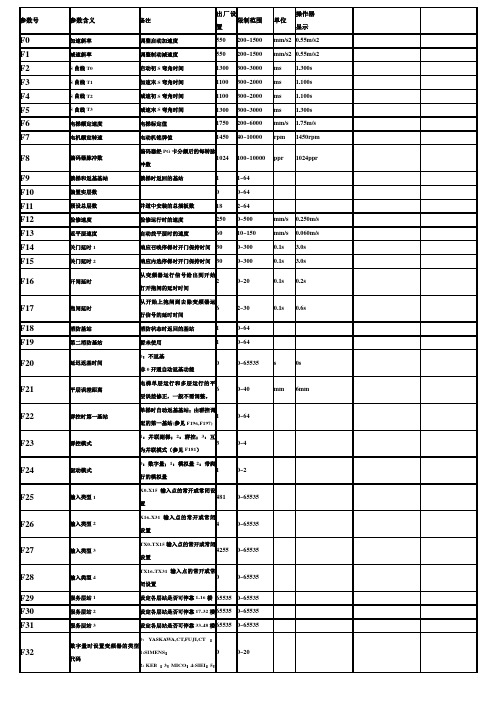
自动运行间隔
5
0~60
s
5s
F34
自动运行次数
0
0~65535
F35
消防模式
0:中国标准(包括港、澳);
0
0~3
F36
抱闸开关触点检测模式
0:无检测;1:大陆检测模式;2:香港检测模式
0
0~65535
F37~F40
备用
F41
DTZ-III-DC-SC型称重装置空满载学习,参看F164 = 0,3.
5500
0~65535
mm
5.500m
F158
五层减速距离
只有五个段速时也是多层减速距离,只有四个以下段速时不用
6500
0~65535
mm
6.500m
F160
是否开通人工去除错误指令功能
1-开通0-不开通
1
0~65535
F161
是否开通时间段楼层封锁功能
1-仅开通楼层指令封锁2-仅开通楼层外呼封锁,3-开通楼层指令和外呼封锁.0-不开通.
返平层速度
自动找平层时的速度
60
10~150
mm/s
0.060m/s
F14
关门延时1
响应召唤停梯时开门保持时间
30
0~300
0.1s
3.0s
F15
关门延时2
响应内选停梯时开门保持时间
30
0~300
0.1s
3.0s
F16
开闸延时
从变频器运行信号给出到开始打开抱闸的延时时间
2
0~20
0.1s
0.2s
F17
0
0~65535
F56
上平层调整
新时达F5021说明手册

第二章 串行控制系统简介 .......................................................................................................................................... 10
2.3.1 主控制板........................................................................................................................................................ 12 2.3.2 轿厢控制板.................................................................................................................................................... 16 2.3.3 指令控制板.................................................................................................................................................... 20 2.3.4 召唤控制板&显示控制板 ............................................................................................................................. 22 2.3.5 群控板 SM-GC .............................................................................................................................................. 31
FYD-5021KLX-XX中文资料

PartNO.:FYD-5021KX/LX-XXADD:NO.115QiXin Road NingBo Zhejiang China ZIP.:315051DESCRIPTION●12.70mm (0.50”)Dual digit numeric display series.●Standard brightness.●Low current operation.●Excellent character apperance.●Easy mounting on P.C.boards or socketsPackage Dimensions &Internal Circuit DiagramNotes:·All dimensions are in millimeters (inches)·Tolerance is ±0.25(0.01")unless otherwise noted.·Specificaions are subject to change whitoutnotice.PartNO.:FYD-5021KX/LX-XXADD:NO.115QiXin Road NingBo Zhejiang China ZIP.:315051:Absolute maximum ratings (Ta=25℃)ValueParameter Symbol Test ConditionMinMaxUnitReverse V oltage VR IR=30μA 5-----V ForwardCurrentIF -----------30mA Power Dissipation Pd -----------100mW Pulse Current Ipeak Duty=0.1mS,1KHz ------150mA Operating Temperature Topr ------40+85°C Storage TemperatureTstr------40+85°C■Description:·Color Code &Chip characteristics:(Test Condition:IF=20mA)Forward Voltage(VF)Unit:V Emitting Color Dice Material PeakWaveLength (λP )Spectral Line halfwidth(△λ1/2)Typ Max Luminous Intensity (Iv)Unit:ucd HRed GaP/GaP700nm 90nm 2.25 2.50500S Hi Red GaAlAs/GaAs,SH 660nm 20nm 1.85 2.203500D Super Red GaAlAs/GaAs,DH 660nm 20nm 1.85 2.206000UR Ultra Red GaAlAs/GaAs,DD H660nm 20nm 1.85 2.2012000E Orange GaAsP/GaP 635nm 35nm 2.10 2.502500Y Yellow GaAsP/GaP 585nm 35nm 2.10 2.502000GGreenGaP/GaP570nm30nm2.202.502500·-XX:Surface /Lens color :Number12345Ref Surface Color White Black Gray Red Green Epoxy ColorWater clearWhite diffusedRed DiffusedGreen DiffusedYellow DiffusedPartNO.:FYD-5021KX/LX-XXADD:NO.115QiXin Road NingBo Zhejiang China ZIP.:3150511.00.53504004505005506006507007508008509009501000(A)(B)(C)(D)(2)(3)(8)(4)(1)(6)(5)(9)(10)Wavelength(nm)RELATIVE INTENSITY Vs WAVELENGTH()λp (1)-GaAsP/GaAs 655nm/Red (2)-GaP 570nm/Yellow Green (3)-GaAsP/GaP 585nm/Yellow(4)-GaAsp/GaP 635nm/Orange &Hi-Eff Red (5)-GaP 700nm/Bright Red(6)-GaAlAs/GaAs 660nm/Super Red (8)-GaAsP/GaP 610nm/Super Red(9)-GaAlAs 880nm(10)-GaAs/GaAs &GaAlAs/GaAs 940nm (A)-GaN/SiC 430nm/Blue (B)-InGaN/SiC 470nm/Blue(C)-(D)-InGaN/SiC 505nm/Ultra Green InGaAl/SiC 525nm/Ultra Green504030201001.21.62.0 2.4 2.63.016345285040302010020406080100162,4,8,A 353210.50.20.1-30-20-10102030405060701542310987654321110100100010,00010KHz 3KHz1KHz 300KHz 100KHz F-REFRESH RATE100KHz 30KHz10KHz 3KHz 1KHz 300Hz 100Hz 10987654321110100100010,000FORWARD VOLT AGE (Vf)FORWARD CURRENT VS.FORWARD VOLTAGERELATIVE LUMINOUSINTENSITY VS.FORWARD CURRENTAMBIENT TEMPERATURE T a()℃FORWARD CURRENT VS.AMBIENT TEMPERATUREtp-PULSE DURATION uS (1,2,3,4,6,8,B.D.J.K)NOTE:25free air temperature unless otherwise specified℃tp-PULSE DURATION uSFORWARD CURRENT(mA)FORWARD CURRENT (mA)RELA TIVE LUMINOUS INTENSITYFORWARD CURRENT(mA)RELATIVE LUMINOUS INTENSITYAMBIENT TEMPERATURE T a()℃(5)Ipeak MAX.IDC MAX.Ipeak MAX.IDC MAX.PartNO.:FYD-5021KX/LX-XXADD:NO.115QiXin Road NingBo Zhejiang China ZIP.:315051tapy QTY/foam(pcs)QTY /Bundle (pcs)QTY /CARTONDimensionFYD-5021KLx-xx 5*13=6565*16=10401040*4=4160。
新宝FGP中文说明书

数字式测力仪使用说明书使用前,请务必阅读使用前,在阅读使用说明书的同时,还要认真阅读“安全注意事项”,做到正确使用。
FGP-0.2/0.5/1/2/5/10/20/50/10092752A日本电产新宝株式会社安全注意事项●阅读完使用说明书后,请务必保管在使用者能随时看得见的地方。
安全注意事项使用时的注意事项1.本产品的特征 42.确认附属品 43.各部位的名称和作用 5 3.1.主体部分 5 3.2.显示部分 63.2.1.各部位名称 63.2.2.数值显示部位 63.2.3.单位显示部位 63.2.4.峰值保持显示部位 63.2.5.MAX・MIN显示部位 64.使用前注意事项 7 4.1.充电 7 4.2.计测头的安装 7 4.3.吊架的安装 7 4.4.跟踪功能 8 4.5.功能设定 84.5.1.设定显示符号:f01 94.5.2.设定显示周期: f02 94.5.3.设定电源自动关闭: f03 94.5.4.设定RS-232C波特率: f04 104.5.5.设定计测过滤: f05 104.5.6.设定外部输出切换: f06 104.5.7.结束功能模式 104.6.上下倒转显示 115.功能及操作 11 5.1.操作概要 11 5.2.计测模式 125.2.1通常计测模式 125.2.2峰值保持模式 12 5.3.单位切换功能 12 5.4.归零功能 12 5.5.比较功能 135.5.1.关于比较功能 135.5.2.比较・存储设定模式的设定方法 135.5.3.设定比较上限值 135.5.4.设定比较下限值 145.5.5.液晶显示比较判定结果 145.5.6.输出比较判定结果 145.6.存储功能 145.6.1.设定存储模式 165.6.2.数据登记方法 175.6.2.1.连续存储模式的数据登记方法 175.6.2.2.单独存储模式的数据登记方法 175.6.2.3.标准存储模式的数据登记方法 17 5.7.存储登记数据显示方法 185.7.1.连续存储模式 185.7.1.1.显示计测值存储数据 185.7.1.2.显示统计数据 195.7.2.单独存储模式 205.7.2.1.显示计测值存储数据 205.7.2.2.显示统计数据 215.7.3.标准存储模式 215.7.3.1.显示计测值存储数据 225.7.3.2.显示统计数据 23 5.8.存储登记数据的删除方法 235.8.1.删除最后一条数据 235.8.2.删除全部数据 245.8.3.无存储登记数据 24 B通信功能 245.9.1.Toriemon USB(中文版)的特征 245.9.2.Toriemon USB(中文版)的下载步骤 24B的使用注意事项 246.外部连接端口 25 6.1.针脚分配 25 6.2.RS-232C输出 256.2.1.RS-232C接口规格 256.2.2.RS-232C的通信命令 266.2.3.连接示例 27 6.3.模拟输出 276.4.过载/比较输出 277.常见问题 28 7.1.无动作、或疑为故障的问题 287.2.其它的一般问题 288.维护支持 29 8.1.关于修理和校正 298.2.保证 299.规格和外形尺寸 29目录-3-4--4- 2.确认附属品1.本产品的特征●采用镍氢电池,故可长时间使用 → 见4.1.充电●使用USB,可向电脑传送数据 → 见B 通信功能●存储功能可存储计测数据(最多可存储1000条) → 见5.6.存储功能●有比较功能,可判断产品是否合格(有判定结果的I/O 输出功能) → 见5.5.比较功能●额定容量2.000N(200.0gf)~1000N(100.0kgf)之间的全系列机种 → 见9.规格和外形尺寸●采用简单操作可实现显示数值和显示单位倒转的倒转式显示 →见4.6.上下倒转显示●一键操作可实现N、kgf(gf)、lbf(ozf)等各单位的切换→见5.3.单位切换功能●可分别计测正值和负值的峰值(峰值保持)→见5.2.2.峰值保持模式●1000次/秒的高速峰值计测→ 见5.2.2.峰值保持模式●最高可从20次/秒选择计测次数(表示周期)→ 见5.2.1.通常计测模式-5-3.各部分的名称和作用 3.1.主体部分①計測軸施加推拉力的螺栓。
BP5021资料

C1 is a slow-start capacitor for mitigating the excessive rush current that flows into the hybrid IC when the switch is turned on.
317
元器件交易网 Regulator ICs
FOperation notes (1) The output current should be reduced according to an increase in the input voltage or ambient temperature. Use the IC within the derating curve range. (2) Pins 5 and 7 are not used. (3) No circuit is installed in the IC to protect against excessive output currents. Take physical safety measures such as fusing if short-circuit loading is probable. (4) A large rush current may flow in the IC when the input voltage is applied or the output ON / OFF is controlled with pin 4 without a capacitor such as C1 in application 2. Comply with the safe operation ranges shown in Figs. 13, 16, and 19. FElectrical characteristic curves For the BP5020
FJP5021中文资料

FJP5021NPN Silicon TransistorAbsolute Maximum Ratings T C =25°C unless otherwise notedElectrical Characteristics T C =25°C unless otherwise notedh FE ClassificationSymbol ParameterValue Units V CBO Collector-Base Voltage 800V V CEO Collector-Emitter Voltage 500V V EBO Emitter-Base Voltage 7V I C Collector Current (DC) 5A I CPCollector Current (Pulse) 10A I BBase Current2A P C Collector Dissipation (T C =25°C) 50W T J Junction Temperature 150°C T STGStorage Temperature- 55 ~ 150°CSymbol ParameterTest Condition Min.Typ.Max.Units BV CBO Collector-Base Breakdown Voltage I C = 1mA, I E = 0800V BV CEO Collector-Emitter Breakdown Voltage I C = 5mA, I B = 0500V BV EBOEmitter-Base Breakdown Voltage I E = 1mA, I C = 0 7V V CEX (sus)Collector-Emitter Sustaining Voltage I C = 2.5A, I B1 = -I B2 = 1A L = 1mH, Clamped 500VI CBO Collector Cut-off Current V CB = 500V, I E = 010µA I EBO Emitter Cut-off Current V EB = 5V, I C = 010µAh FE1 h FE2 DC Current GainV CE = 5V, I C = 0.6A V CE = 5V, I C = 3A 15 850 V CE (sat) Collector-Emitter Saturation Voltage I C = 3A, I B = 0.6A 1V V BE (sat) Base-Emitter Saturation Voltage I C = 3A, I B = 0.6A1.5V C ob Output CapacitanceV CB = 10V, I E = 0, f=1MHz 80pF f T Current Gain Bandwidth Product V CE = 10V, I C = 0.6A 18MHz t ON Turn On Time V CC = 200VI C = 5I B1 = -2.5I B2 = 4A R L = 50Ω0.5µs t STG Storage Time 3µs t FFall Time0.10.3µsClassificationR O Y h FE115 ~ 3020 ~ 4030 ~ 50FJP5021High Voltage and High Reliability•High Speed Switching : t F = 0.1µs (Typ.)•Wide SOA1.Base2.Collector3.Emitter1TO-220FJP5021TRADEMARKSThe following are registered and unregistered trademarks Fairchild Semiconductor owns or is authorized to use and is not intended to be an exhaustive list of all such trademarks.DISCLAIMERFAIRCHILD SEMICONDUCTOR RESERVES THE RIGHT TO MAKE CHANGES WITHOUT FURTHER NOTICE TO ANY PRODUCTS HEREIN TO IMPROVE RELIABILITY, FUNCTION OR DESIGN. FAIRCHILD DOES NOT ASSUME ANY LIABILITY ARISING OUT OF THE APPLICATION OR USE OF ANY PRODUCT OR CIRCUIT DESCRIBED HEREIN;NEITHER DOES IT CONVEY ANY LICENSE UNDER ITS PATENT RIGHTS, NOR THE RIGHTS OF OTHERS.LIFE SUPPORT POLICYFAIRCHILD’S PRODUCTS ARE NOT AUTHORIZED FOR USE AS CRITICAL COMPONENTS IN LIFE SUPPORT DEVICES OR SYSTEMS WITHOUT THE EXPRESS WRITTEN APPROVAL OF FAIRCHILD SEMICONDUCTOR CORPORATION.As used herein:1. Life support devices or systems are devices or systems which, (a) are intended for surgical implant into the body,or (b) support or sustain life, or (c) whose failure to perform when properly used in accordance with instructions for use provided in the labeling, can be reasonably expected to result in significant injury to the user.2. A critical component is any component of a life support device or system whose failure to perform can be reasonably expected to cause the failure of the life support device or system, or to affect its safety or effectiveness.PRODUCT STATUS DEFINITIONS Definition of TermsDatasheet Identification Product Status DefinitionAdvance InformationFormative or In Design This datasheet contains the design specifications for product development. Specifications may change in any manner without notice.PreliminaryFirst ProductionThis datasheet contains preliminary data, andsupplementary data will be published at a later date.Fairchild Semiconductor reserves the right to make changes at any time without notice in order to improve design.No Identification Needed Full ProductionThis datasheet contains final specifications. Fairchild Semiconductor reserves the right to make changes at any time without notice in order to improve design.Obsolete Not In ProductionThis datasheet contains specifications on a product that has been discontinued by Fairchild semiconductor.The datasheet is printed for reference information only.FACT™FACT Quiet series™FAST ®FASTr™FRFET™GlobalOptoisolator™GTO™HiSeC™I 2C™ImpliedDisconnect™ISOPLANAR™LittleFET™MicroFET™MicroPak™MICROWIRE™MSX™MSXPro™OCX™OCXPro™OPTOLOGIC ®OPTOPLANAR™PACMAN™POP™Power247™PowerTrench ®QFET™QS™QT Optoelectronics™Quiet Series™RapidConfigure™RapidConnect™SILENT SWITCHER ®SMART START™SPM™Stealth™SuperSOT™-3SuperSOT™-6SuperSOT™-8SyncFET™TinyLogic ®TruTranslation™UHC™UltraFET ®VCX™ACEx™ActiveArray™Bottomless™CoolFET™CROSSVOLT ™DOME™EcoSPARK™E 2CMOS™EnSigna™Across the board. Around the world.™The Power Franchise™Programmable Active Droop™。
福乐斯材料简介快速版

我公司为福乐斯的一级代理商,可为您提供福乐斯橡塑发泡保温材料。
零级福乐斯:闭泡,柔性,灰色,丁腈橡胶为基材,通过零级防火标准,优异隔热性能。
可提供管材,板材和胶带。
一级福乐斯:闭泡,柔性,黑色,丁腈橡胶为基材,通过一级防火标准及国标防火要求,优异隔热性能。
优秀阻湿性能。
可提供管材、管材和胶带。
HT福乐斯:闭泡结构,良好的耐候性,三元乙丙为基材,最高的工作温度达到150℃。
NH福乐斯:不含卤素,闭泡结构,丁腈橡胶为基材,具有非常低的毒性,具有多项船级社认证。
福乐斯管道支撑:福乐斯保温材料符合硬质支撑材料外敷铝合金外壳,可有效防止冷/热桥的产生。
福乐斯管道支撑是冷管线完全隔绝水汽和放凝露的最佳选择。
福乐斯附件产品:福乐斯520胶水作为福乐斯的专用粘结剂,福乐斯625胶水是高温福乐斯的专用粘结剂。
福乐斯820胶水是福乐斯国产胶水。
福乐斯防晒漆,用于室外施工中保护福乐斯不受紫外线伤害。
福乐斯材料的保障系统:1 防止水汽渗透:福乐斯多层的闭泡结构构成了一个防潮层,即使材料表面出现小孔或裂口,福乐斯保温材料不会受到水汽的威胁。
这样福乐斯保温系统终生都得到抗水汽的保证。
2 长期稳定的热阻性能:因为没有毛细作用和福乐斯闭泡结构,使得水汽不能渗透到福乐斯保温层里,水汽不能通过专业熟练安装的福乐斯保温材料。
3 超长的使用寿命:没有脆弱的隔气层-福乐斯本身的结构使得终生具有优异的隔汽性能。
4 避免产生“冷/热”桥现象:福乐斯保温系统是严密的系统,其自身具有的技术性能提供了安全保证。
5 防霉:福乐斯防霉首先要求减少水汽的渗入。
第二个要求没有纤维,光滑表面不易存留灰尘。
6 不含甲醛:您可以确信福乐斯是基本上不挥发的材料,同时它含有的有机挥发物也非常少。
7 健康和室内空气质量的保障:福乐斯无粉尘无纤维即使切割成各种形状和管件也不挥发有害气体和纤维不含氟利昂和氢化氟利昂等有害物质8 生产的监督和技术评估:福乐斯产品拥有FM认证管理-承诺监控产品与公布的技术性能的一致性优异的防护性能优异的阻湿性能稳定的导热系数9 质量保准的监督:ISO注册机构确认阿乐斯公司在管理质量控制过程上达到客户要求。
502胶水参数

502胶水参数
性能丙烯酸酯胶。
单组份.由α-氰基丙烯酸乙酯、增塑剂、增调剂、稳定剂等组成。
固化速度极快,瞬间即能固化,施工工艺简单。
具有较高的胶接强度。
能胶接多种材料。
但脆性较大,咬接持久性及耐水性较差。
外观无色透明液体
粘度(MPa·s) 2~10
密度(g/cm3) 1.06
折射率 1.4373
表面张力(×10-5N/cm) 35.1
剪切强度(MPa) 13~15
拉伸强度,MPa) >25
应用领域通用型粘合剂。
使用温度范围-50~70℃。
广泛用于钢、铜、铝、橡胶、硬塑料、有机玻璃、聚苯乙烯、电木、木材、陶瓷、玻璃等材料的胶接。
但不宜用于大面积或间隙较大场合的胶接。
快速OPEX主板F5021 1.5V中文说明

2: KEB
3: MICO
4: SIEI
5: Dietz
0
33
自动运行间隔
5
s
5s
34
自动运行次数
0
35
消防模式
0:中国标准
1:苏州迅达模式(仅区别于消防时允许关门)
0
36
抱闸开关检测模式
0:没有抱闸开关设置
1:在除香港以外的其它地区使用
2:在香港地区使用
43
司机状态外呼蜂鸣闪烁功能选择
参数
参数含义
备注
出厂值
单位
读做
0
加速斜率
调整启动加速度
550
mm/s2
0.55m/ s2
1
减速斜率
调整制动减速度
550
mm/s2
0.55m/ s2
2
S曲线T0
启动初S弯角时间
1300
0.01s
1.300s
3
S曲线T1
加速末S弯角时间
1100
0.01s
1.100s
4
S曲线T2
减速初S弯角时间
1100
0.01s
注:不接手持编程器时严禁将J2短接.
LED指示灯:上排是输入信号指示灯,从左到右为: X0,X1,...,... X25
下排右上方是高压输入信号指示灯,从上到下为: X26,X27,X28,X29
下排是输出信号指示灯,从左到右为:Y0, Y1, Y2, ...,... Y14, Y15
2.主板参数说明(配无参数分类操作器使用)
只有一个段速时也是多层减速距离
1300
mm
1.300m
46
双层或多层减速距离
F5021调试说明书

解读井道数据(监视状态)的含义: 单位mm1: 下端站平层基准位置0 mm 2: 2 楼平层离开下端站平层位置(mm)3: 3 楼平层离开下端站平层位置(mm)4: 4 楼平层离开下端站平层位置(mm)...64: 64楼平层离开下端站平层位置(mm)65: 平层插板的长度(以 2 楼的插板为基准,mm)66: 平层感应器间距(mm)67: 上行 1 级减速开关到上端站的距离(mm)68: 上行 2 级减速开关到上端站的距离(mm)69: 上行 3 级减速开关到上端站的距离(mm)70: 上行 4 级减速开关到上端站的距离(mm)71: 下行 1 级减速开关到下端站的距离(mm)72: 下行 2 级减速开关到下端站的距离(mm)73: 下行 3 级减速开关到下端站的距离(mm)74: 下行 4 级减速开关到下端站的距离(mm)作用1、检查参数F182(减速开关级数) 以及输入类型设置是否正确2、自学习后检查减速开关的距离是否符合规定3、自学习两遍检查两次自学习的楼层数据是否一致(最大误差<= 3mm),以排除编码器干扰二: 平层调不好的原因有一些现场反映平层调不好,经过总结有如下问题,请按顺序检查1: 以下参数设置不合理会导致平层调不好检查F21(平层感应器延迟调整),出厂值 6 mm. 1.75m/s 以下电梯使用光电平层感应器时都可以设置为6mm高速电梯(3.0m/s 或以上)使用光电平层感应器时都可以设置为10 mm高速电梯(5.0m/s 或以上)使用光电平层感应器时都可以设置为16 mmF56 上行平层调整,出厂值50 mmF57 下行平层调整,出厂值50 mm平层微调:把每一层平层平层微调都设置为出厂值20 mm2: 编码器干扰1) 编码器屏蔽线没有接地,或者信号线和动力线不分开,受到动力线的干扰。
这个问题在同步电机现场更为严重。
Sincos 编码器或旋转变压器是小模拟量信号,比较容易受干扰。
LM500F、510F技术说明书07.07
FLA_502说明书(含通信协议)
FLA-502汽车排气分析仪使用说明书Va.3粤制06000117号-1市福立分析仪器市福立分析仪器分公司■目录前言 (3)质量保证承若及责任 (3)名称与功能 (5)●前视图 (5)●后视图 (5)测量前准备 (6)●连接取样元件和排气管 (6)●检查过滤元件 (6)●检查保险丝 (7)●检查电源 (7)●气管连接 (7)日常操作与测量 (8)日常操作 (8)●动作检查 (8)●泄漏检查 (9)●H C吸附测试 (10)●时钟设置 (11)●符号选择 (11)●通讯设置 (11)●燃料H/C设置 (12)●转速信息设置 (12)●校准 (13)●零气选择 (13)●标定 (14)状态检查 (17)简易诊断 (18)维修注意事项 (19)元件更换 (19)●过滤元件的更换 (19)●传感器的更换 (19)保养检查 (21)技术参数 (22)输出信号说明 (24)■前言本公司生产的FLA-502汽车排气分析仪采用具有国际水平的进口红外检测器,该仪器能同时测定汽车排气中的HC、CO、CO2、或/和O2、NO四组份或五组份之浓度值,还可以测试汽车发动机转速、空燃比及机油温度,环境温度与湿度、大气压力。
FLA-502采用大屏幕液晶显示,全中文提示,多燃料测试,有多种测量模式,包括双怠速测试。
其中:HC、CO、CO2组份检测采用不分光红外检测器,NO组份检测可采用不分光红外检测器(使用寿命长,响应速度快)或电化学传感器(NO检测器根据用户需要选择安装),O2采用电化学传感器。
为了能正确使用仪器,在使用之前请仔细阅读本使用说明书,并请妥善保管,以备需要时查阅。
■质量保证承诺及责任您所购买的FLA-502汽车排气分析仪享有市福立分析仪器提供的一年保修期。
在此期间,仪器如有任何属于本公司责任的故障,我们将会为您免费维修或更换零件。
此保修围不包括以下几点:由于使用不当而无常工作的;由于不是本公司授权的任何单位或个人所修理过或改变过而不能正常工作的;由于在不适宜的工作环境下使用而引起不能正常工作;由于意外事故而引起的不能正常工作;由于跌落而造成的不能正常工作;市福立分析仪器任何时候都保留有对该产品及其设计或本使用说明书进行更改的权利,如有更改,恕不另行通知。
LM5021MM-1中文资料
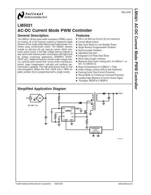
LM5021AC-DC Current Mode PWM ControllerGeneral DescriptionThe LM5021off-line pulse width modulation (PWM)control-ler contains all of the features needed to implement highly efficient off-line single-ended flyback and forward power con-verters using current-mode control.The LM5021features include an ultra-low (25µA)start-up current,which mini-mizes power losses in the high voltage start-up network.A skip cycle mode reduces power consumption with light loads for energy conserving applications (ENERGY STAR ®,CECP ,etc.).Additional features include under-voltage lock-out,cycle-by-cycle current limit,hiccup mode overload pro-tection,slope compensation,soft-start and oscillator syn-chronization capability.This high performance 8-pin IC has total propagation delays less than 100nS and a 1MHz ca-pable oscillator that is programmed with a single resistor.Featuresn Ultra Low Start-up Current (25µA maximum)n Current Mode Controln Skip Cycle Mode for Low Standby Power n Single Resistor Programmable Oscillator n Synchronizable Oscillator n Adjustable Soft-startn Integrated 0.7A Peak Gate Driver n Direct Opto-Coupler Interfacen Maximum Duty Cycle Limiting (80%for LM5021-1or 50%for LM5021-2)n Slope Compensation for (LM5021-1Only)n Under Voltage Lockout (UVLO)with Hysteresis n Cycle-by-Cycle Over-Current Protectionn Hiccup Mode for Continuous Overload Protection n Leading Edge Blanking of Current Sense Signal nPackages:MSOP-8or MDIP-8Simplified Application Diagram20144201May 2005LM5021AC-DC Current Mode PWM Controller©2005National Semiconductor Corporation Connection DiagramTop View20144202MSOP-8and MDIP-8Ordering InformationOrder Number Description Package Type Supplied AsLM5021MM-180%Duty Cycle Limit MSOP-8Available Soon LM5021MMX-180%Duty Cycle Limit MSOP-8Available Soon LM5021NA-180%Duty Cycle Limit MDIP-840Units per Rail LM5021MM-250%Duty Cycle Limit MSOP-8Available Soon LM5021MMX-250%Duty Cycle Limit MSOP-8Available Soon LM5021NA-250%Duty Cycle LimitMDIP-840Units per RailPin DescriptionPIN NAME DESCRIPTIONAPPLICATION INFORMATION1COMP Control input for the Pulse Width Modulator and Hiccup P pull-up is provided by an internal 5K resistor which may be used to bias an opto-coupler transistor.2VIN Input voltage.Input to start-up regulator.The VIN pin is clamped at 36V by an internal zener diode.3VCCOutput of a linear bias supply regulator.Nominally 8.5V.VCC provides bias to controller and gate drive sections of the LM5021.An external capacitor must be connected from this pin to ground.4OUTMOSFET gate driver output.High current output to the external MOSFET gate input with source/sink current capability of 0.3A and 0.7A respectively.5GND Ground return.6CSCurrent Sense input.Current sense input for current mode control andover-current protection.Current limiting is accomplished using a dedicated current sense comparator.If the CS comparator input exceeds 0.5Volts the OUT pinswitches low for cycle-by-cycle current limit.CS is held low for 90ns after OUT switches high to blank the leading edge current spike.7RT /SYNC Oscillator timing resistor pin andsynchronization input.An external resistor connected from RT to GND sets the oscillator frequency.This pin will also accept synchronization pulses from an external clock.8SSSoft-start /Hiccup timeAn external capacitor and an internal 22µA current source set the soft-start ramp.The soft -start capacitor controls both the soft-start rate and the hiccup mode period.L M 5021 2Absolute Maximum Ratings(Note1)If Military/Aerospace specified devices are required, please contact the National Semiconductor Sales Office/ Distributors for availability and specifications.VIN to GND-0.3V to30V VIN Clamp Continuous Current5mA CS to GND-0.3V to1.25V RT to GND-0.3V to5.5V All other pins to GND-0.3V to7.0VESD Rating(Note2)Human Body Model2kV Storage Temperature-65˚C to+150˚C Operating Junction Temperature+150˚COperating Ratings(Note1)VIN Voltage(Note5)8V to30V Junction Temperature-40˚C to+125˚CElectrical Characteristics Specifications in standard type face are for TJ=+25˚C and those in boldfacetype apply over the full Operating Junction Temperature Range.Unless otherwise specified:V IN=15V,R T=44.2KΩ.(Note3)Symbol Parameter Conditions Min Typ Max Unit STARTUP CIRCUITStart Up Current Before VCC Enable1825µAVCC Regulator enable threshold172023VVCC Regulator disablethreshold7.25VVIN ESD Clamp voltage I=5mA303640VI VIN Operating supply current COMP=0VDC 2.5 3.75mAVCC SUPPLYController enable threshold 6.577.5VController disable threshold 5.3 5.8 6.3VVCC regulated output No External Load88.59VVCC dropout voltage(VIN-VCC)I=5mA 1.7VVCC regulator current limit VCC=7.5V(Note4)1522mASKIP CYCLE MODE COMPARATORSkip Cycle mode enablethreshold1⁄3[COMP-1.25V]75125175mV Skip Cycle mode hysteresis5mV CURRENT LIMITCS limit to OUT delay CS stepped from0to0.6V,time to OUTtransition low,C load=0.35nsCS limit threshold0.450.50.55VLeading Edge Blanking time90nsCS blanking sinking impedance3555ΩSOFT-STARTV SS-OCV SS pin open-circuit voltage 4.3 5.2 6.1V Soft-start Current Source152230µASoft-start to COMP Offset0.350.550.75VCOMP sinking impedance During SS ramp60ΩOSCILLATORFrequency1(RT=44.2K)135150165kHzFrequency2(RT=13.3K)440500560kHzSync threshold 2.4 3.2 3.8VLM50213Electrical Characteristics Specifications in standard type face are for T J =+25˚C and those in boldface typeapply over the full Operating Junction Temperature Range .Unless otherwise specified:V IN =15V,R T =44.2K Ω.(Note 3)(Continued)SymbolParameterConditionsMinTypMaxUnitPWM COMPARATORCOMP to OUT delayCOMP set to 2V CS stepped 0to 0.4V,time to OUT transition low,C load =0.20nsMin Duty CycleCOMP =0V0%Max Duty Cycle (-1Device)758085%Max Duty Cycle (-2Device)50%COMP to PWM comparator gain 0.33COMP Open Circuit Voltage 4.25.16V COMP at Max Duty Cycle 2.75V COMP Short Circuit CurrentCOMP =0V 0.6 1.1 1.5mA SLOPE COMPENSATIONSlope Comp Amplitude (LM5021-1only)CS pin to PWMComparator offset at maximum duty cycle 7090110mVOUTPUT SECTIONOUT High Saturation IOUT =50mA,VCC -OUT0.6 1.1V OUT Low Saturation IOUT =100mA 0.31V Peak Source Current OUT =VCC/2.0.3A Peak Sink Current OUT =VCC/2.0.7A Rise time C load =1nF 25ns Fall timeC load =1nF 10ns HICCUP MODE V OVLD Over load detection threshold COMP pin V SS-OCV –0.8V SS-OCV –0.6V SS-OCV –0.4V V HIC Hiccup mode threshold SS pin V SS-OCV –0.8V SS-OCV –0.6V SS-OCV –0.4V V RST Hiccup mode Restart threshold SS pin0.10.30.5V I DTCS Dead-time current source 0.10.250.4µA I OVCSOverload detection timer current source61014µATHERMAL RESISTANCEθJA MSOP-8Junction to Ambient 0LFM 200˚C/W θJAMDIP-8Junction to Ambient0LFM107˚C/WNote 1:Absolute Maximum Ratings are limits beyond which damage to the device may occur.Operating Ratings are conditions under which operation of the device is intended to be functional.For guaranteed specifications and test conditions,see the Electrical Characteristics.Note 2:The human body model is a 100pF capacitor discharged through a 1.5k Ωresistor into each pin.Note 3:Min and Max limits are 100%production tested at 25˚C.Limits over the operating temperature range are guaranteed through correlation using Statistical Quality Control (SQC)methods.Limits are used to calculate National’s Average Outgoing Quality Level (AOQL).Note 4:Device thermal limitations may limit usable range.Note 5:After initial turn-on at VIN =20V.L M 5021 4LM5021 Simplified Block Diagram20144203FIGURE1.5Typical Performance CharacteristicsUnless otherwise specified:T J =25˚C.VIN Start-Up CurrentVIN UVLO2014420420144205VIN Current vs OUT Load VIN Voltage Falling vs VCC Voltage2014420620144207OUT Driver Current vs Temperature Hiccup Mode Deadtime vs Softstart Capacitance2014420820144209L M 5021 6Typical Performance Characteristics Unless otherwise specified:T J =25˚C.(Continued)Output Switching Frequency vs RT20144210Detailed Operating DescriptionSTART UP CIRCUITReferring to Figure 2,the input capacitor C VIN is trickle charged through the start-up resistor Rstart,when the recti-fied ac input voltage HV is applied.The VIN current con-sumed by the LM5021is only 18µA (nominal)while the capacitor C VIN is initially charged to the start-up threshold.When the input voltage,VIN reaches the upper VIN UVLO threshold of 20V,the internal VCC linear regulator is en-abled.The VCC regulator will remain on until VIN falls to the lower UVLO threshold of 7.25V (12.5V hysteresis).When the VCC regulator is turned on,the external capacitor at the VCC pin begins to charge.The PWM controller,soft-start circuit and gate driver are enabled when the VCC voltage reaches the VCC UVLO upper threshold of 7V.The VCC UVLO has 1.2V hysteresis between the upper and lowerthresholds to avoid chattering during transients on the VCC pin.When the VCC UVLO enables the switching power supply,energy is transferred from the primary to the second-ary transformer winding(s).A bias winding,shown in Figure 2,delivers power to the VIN pin to sustain the VCC regulator.The voltage supplied should be from 11V (VCC regulated voltage maximum plus VCC regulator dropout voltage)to 30V (maximum operating VIN voltage).The start-up se-quence is completed and normal operation begins when the voltage from the bias winding is sufficient to maintain VCC level greater than the VCC UVLO threshold (5.8V typical).The size of the start-up resistor Rstart not only affects power supply start-up time,but also power supply efficiency since the resistor dissipates power in normal operation.The ultra low start-up current of the LM5021allows a large value Rstart resistor (up to 3M Ω)for improved efficiency with reasonable start-up time.20144211FIGURE 2.Start-Up Circuit Block DiagramLM50217Detailed Operating Description(Continued)RELATIONSHIP BETWEEN INPUT CAPACITOR C IN &V CC CAPACITOR C VCCThe internal VCC linear regulator is enabled when VIN reaches 20V.The drop in VIN due to charge transfer from C VIN to C VCC after the regulator is enabled can be calculated from the following equations where VIN’is the voltage on C VIN immediately after the VCC regulator charges C VCC .∆VIN x C VIN =∆VCC x C VCC (20V –V IN’)C VIN =8.5V C VCCAssuming C VIN value as 10µF,and C VCC of 1µF,then the drop in VIN will be 0.85V,or the VIN value drops to 19.15V.The value of the VCC capacitor can be small (less than 1uF)as it supplies only transient gate drive current of a short duration.The C VIN capacitor must be sized to supply the gate drive current and the quiescent current of LM5021until the transformer bias winding delivers sufficient voltage to VIN to sustain the VCC voltage.The C VIN capacitor value can be calculated from the operat-ing VCC load current after it’s output voltage reaches the VCC UVLO threshold.For example,if the LM5021is driving an external MOSFET with total gate charge (Qg)of 25nC,the average gate drive current is Qg x Fsw,where Fsw is the switching frequency.Assuming a switching frequency of 150KHz,the average gate drive current is 3.75mA.Since the IC consumes approximately 2.5mA operating current in ad-dition to the gate current,the total current drawn from C VIN capacitor is the operating current plus the gate charge cur-rent,or 6.25mA.The C VIN capacitor must supply this current for a brief time until the transformer bias winding takes over.The C VIN voltage must not fall below 8.5V during the start-up sequence or the cycle will be restarted.The maximum allow-able start-up time can be calculated using the value of C VIN ,the change in voltage allow at VIN (19.15V –8.5V)and the VCC regulator current (6.25mA).Tmax,the maximum time allowed to energize the bias winding is:If the calculated value of Tmax is too small,the value of Cin should be increased further to allow more time before the transformer bias winding takes over and delivers the oper-ating current to the VCC regulator.Increasing C VIN will in-crease the time from the application of the rectified ac (HV in the Figure 2)to the time when VIN reaches the 20V start threshold.The initial charging time of C VIN is:PWM COMPARATOR/SLOPE COMPENSATIONThe PWM comparator compares the current sense signal with the loop error voltage from the COMP pin.The COMP pin voltage is reduced by 1.25V then attenuated by a 3:1resistor divider.The PWM comparator input offset voltage is designed such that less than 1.25V at the COMP pin will result in a zero duty cycle at the controller output.For duty cycles greater than 50percent,current mode con-trol circuits are subject to sub-harmonic oscillation.By add-ing an additional fixed slope voltage ramp signal (slope compensation)to the current sense signal,this oscillation can be avoided.The LM5021-1integrates this slope com-pensation by summing a ramp signal generated by the os-cillator with the current sense signal.The slope compensa-tion is generated by a current ramp driven through an internal 1.8k Ωresistor connected to the CS pin.Additional slope compensation may be added by increasing the resis-tance between the current sense filter capacitor and the CS pin,thereby increasing the voltage ramp created by the oscillator current ramp.Since the LM5021-2is not capable of duty cycles greater than 50%,there is no slope compensa-tion feature in this device.CURRENT LIMIT/CURRENT SENSEThe LM5021provides a cycle-by-cycle over current protec-tion feature.Current limit is triggered by an internal current sense comparator threshold which is set at 500mV.If the CS pin voltage plus the slope compensation voltage exceeds 500mV,the OUT pin output pulse will be immediately termi-nated.An RC filter,located near the LM5021,is recommended for the CS pin to attenuate the noise coupled from the power FET’s gate to source.The CS pin capacitance is discharged at the end of each PWM clock cycle by an internal switch.The discharge switch remains on for an additional 90ns leading edge blanking interval to attenuate the current sense transient that occurs when the external power FET is turned on.In addition to providing leading edge blanking,this circuit also improves dynamic performance by discharging the cur-rent sense filter capacitor at the conclusion of every cycle.The LM5021CS comparator is very fast,and may respond to short duration noise yout considerations are critical for the current sense filter and sense resistor.The capacitor associated with the CS filter must be placed very close to the device and connected directly to the pins of the IC (CS and GND).If a current sense transformer is used,both leads of the transformer secondary should be routed to the sense resistor,which should also be located close to the IC.If a current sense resistor located in the power FET’s source is used for current sense,a low inductance resistor is required.In this case,all of the noise sensitive low current grounds should be connected in common near the IC and then a single connection should be made to the power ground (sense resistor ground point).OSCILLATOR,SHUTDOWN and SYNC CAPABILITYA single external resistor connected between RT and GND pins sets the LM5021oscillator frequency.The LM5021-2device,with 50%maximum duty cycle,includes an internal flip-flop that divides the oscillator frequency by two.This method produces a precise 50%maximum duty cycle limit.Because of this frequency divider,the oscillator frequency of the LM5021-2is actually twice the frequency of the gate drive output (OUT).For the LM5021-1device,the oscillatorL M 5021 8Detailed Operating Description(Continued)frequency and the operational output frequency are the same.To set a desired output switching frequency (Fsw),the RT resistor can be calculated from:LM5021-1:LM5021-2:The LM5021can also be synchronized to an external clock.The external clock must have a higher frequency than the free running oscillator frequency set by the RT resistor.The clock signal should be capacitively coupled into the RT pin with a 100pF capacitor.A peak voltage level greater than 3.8Volts at the RT pin is required for detection of the sync pulse.The dc voltage across the RT resistor is internally regulated at 2volts.Therefore,the ac pulse superimposed on the RT resistor must have 1.8V or greater amplitude to successfully synchronize the oscillator.The sync pulse width should be set between 15ns to 150ns by the external components.The RT resistor is always required,whether the oscillator is free running or externally synchronized.The RT resistor should be located very close to the device and connected directly to the pins of the LM5021(RT and GND).GATE DRIVER and MAX DUTY CYCLE LIMITThe LM5021provides a gate driver (OUT),which can source peak current of 0.3A and sink 0.7A.The LM5021is available in two duty-cycle limit options.The maximum output duty-cycle is typically 80%for the LM5021-1option,and precisely equal to 50%for the LM5021-2option.The maximum duty cycle function for the LM5021-2is accomplished with an internal toggle flip-flop to ensure an accurate duty cycle limit.The internal oscillator frequency of the LM5021-2is there-fore twice the switching frequency of the PWM controller (OUT pin).The 80%maximum duty-cycle function for the LM5021-1is determined by the internal oscillator.For the LM5021-1the internal oscillator frequency and the switching frequency of the PWM controller are the same.SOFT-STARTThe soft-start feature allows the power converter to gradually reach the initial steady state operating point,thus reducing start-up stresses and current surges.An internal 22µA current source charges an external capacitor connected to the SS pin.The capacitor voltage will ramp up slowly,limiting the COMP pin voltage and the duty cycle of the output pulses.The soft-start capacitor is also used to generate the hiccup mode delay time when the output of the switching power supply is continuously overloaded.HICCUP MODE OVERLOAD CURRENT LIMITINGHiccup mode is a method of protecting the power supply from over-heating and damage during an extended overload condition.When the output fault is removed the power sup-ply will automatically restart.Figure 3,Figure 4and Figure 5illustrate the equivalent circuit of the hiccup mode for LM5021and the relevant waveforms.During start-up and in normal operation,the external soft-start capacitor Css is pulled up by a current source that delivers 22µA to the SS pin capacitor.In normal operation,the soft-start capacitor continues to charge and eventually reaches the saturation voltage of the current source (V SS_OCV ,nominally 5.2V).During start-up the COMP pin voltage follows the SS capacitor voltage and gradually increases the peak current delivered by the power supply.When the output of the switching power supply reaches the desired voltage,the voltage feedback amplifier takes control of the COMP signal (via the opto-coupler).In normal operation the COMP level is held at an intermediate voltage between 1.25V and 2.75V controlled by the voltage regulation loop.When the COMP pin voltage is below 1.25V,the duty-cycle is zero.When the COMP level is above 2.75V,the duty cycle will be limited by the 0.5V threshold of cycle-by-cycle current limit comparator.If the output of the power supply is overloaded,the voltage regulation loop demands more current by increasing the COMP pin control voltage.When the COMP pin exceeds the over voltage detection threshold (V OVLD ,nominally 4.6V),the SS capacitor Css will be discharged by a 10µA overload detection timer current source,I OVCS .If COMP remains above V OVLD long enough for the SS capacitor to discharge to the Hiccup mode threshold (V HIC ,nominally 4.6V),the controller enters the hiccup mode.The OUT pin is then latched low and the SS capacitor discharge current source is reduced from 10µA to 0.25µA,the dead-time current source,I DTCS .The SS pin voltage is slowly reduced until it reaches the Restart threshold (V RST ,nominally 0.3V).Then a new start-up sequence commences with 22µA current source charging the capacitor C SS .The slow discharge of the SS capacitor from the Hiccup threshold to the Restart threshold provides an extended off time that reduces the overheating of components including diodes and MOSFETs due to the continuous overload.The off time during the hiccup mode can be calculated from the following equation:Example:Toff =808ms,assuming the C SS capacitor value is 0.047µF Short duration intermittent overloads will not trigger the hic-cup mode.The overload duration required to trigger the hiccup response is set by the capacitor C SS ,the 10µA discharge current source and voltage difference between the saturation level of the SS pin and the Hiccup mode thresh-old.Figure 5shows the waveform of SS pin with a short duration overload condition.The overload time required to enter the hiccup mode can be calculated from the following equation:Example:Toverload =2.82ms,assuming the C SS capacitor value is 0.047µFLM50219Detailed Operating Description(Continued)20144219FIGURE 3.Hiccup Mode Control20144220FIGURE 4.Waveform at SS and COMP Pin due to Continuous OverloadL M 5021 10Detailed Operating Description(Continued)SKIP CYCLE OPERATIONDuring light load conditions,the efficiency of the switching power supply typically drops as the losses associated with switching and operating bias currents of the converter be-come a significant percentage of the power delivered to the load.The largest component of the power loss is the switch-ing loss associated with the gate driver and external MOS-FET gate charge.Each PWM cycle consumes a finite amout of energy as the MOSFET is turned on and then turned off. These switching losses are proportional to the frequency of operation.The Skip Cycle function integrated within the LM5021controller reduces the average switching frequency to reduce switching losses and improve efficiency during light load conditions.When a light load condition occurs,the COMP pin voltage is reduced by the voltage feedback loop to reduce the peak current delivered by the controller.Referring to Figure6,the PWM comparator input tracks the COMP pin voltage through a1.25V level shift circuit and a3:1resistor divider.As the COMP pin voltage falls,the input to the PWM comparator falls proportionately.When the PWM comparator input falls to125mV,the Skip Cycle comparator detects the light load condition and disables output pulses from the controller.The controller continues to skip switching cycles until the power supply output falls and the COMP pin voltage increases to demand more output current.The number of cycles skipped will depend on the load and the response time of the fre-quency compensation network.Eventually the COMP volt-age will increase when the voltage loop requires more cur-rent to sustain the regulated output voltage.When the PWM comparator input exceeds130mV(5mV hysteresis),normal fixed frequency switching resumes.Typical power supply designs will produce a short burst of output pulses followed by a long skip cycle interval.The average switching fre-quency in the Skip Cycle mode can be a small fraction of the normal operating frequency of the power supply.20144221FIGURE5.Waveform at SS and COMP Pin due to Brief OverloadLM502111Detailed Operating Description(Continued)20144222FIGURE 6.Skip Cycle ControlL M 5021 12T y p i c a l A p p l i c a t i o n C i r c u i t20144223LM502113Physical Dimensionsinches (millimeters)unless otherwise noted8Lead MSOP Package NS Package Number MUA08A8Lead MDIP Package NS Package Number N08EL M 5021 14NotesNational does not assume any responsibility for use of any circuitry described,no circuit patent licenses are implied and National reserves the right at any time without notice to change said circuitry and specifications.For the most current product information visit us at .LIFE SUPPORT POLICYNATIONAL’S PRODUCTS ARE NOT AUTHORIZED FOR USE AS CRITICAL COMPONENTS IN LIFE SUPPORT DEVICES OR SYSTEMS WITHOUT THE EXPRESS WRITTEN APPROVAL OF THE PRESIDENT AND GENERAL COUNSEL OF NATIONAL SEMICONDUCTOR CORPORATION.As used herein:1.Life support devices or systems are devices or systemswhich,(a)are intended for surgical implant into the body,or(b)support or sustain life,and whose failure to perform whenproperly used in accordance with instructions for use provided in the labeling,can be reasonably expected to result in a significant injury to the user.2.A critical component is any component of a life supportdevice or system whose failure to perform can be reasonably expected to cause the failure of the life support device or system,or to affect its safety or effectiveness.BANNED SUBSTANCE COMPLIANCENational Semiconductor manufactures products and uses packing materials that meet the provisions of the Customer Products Stewardship Specification(CSP-9-111C2)and the Banned Substances and Materials of Interest Specification(CSP-9-111S2)and contain no‘‘Banned Substances’’as defined in CSP-9-111S2.National Semiconductor Americas CustomerSupport CenterEmail:new.feedback@ Tel:1-800-272-9959National SemiconductorEurope Customer Support CenterFax:+49(0)180-5308586Email:europe.support@Deutsch Tel:+49(0)6995086208English Tel:+44(0)8702402171Français Tel:+33(0)141918790National SemiconductorAsia Pacific CustomerSupport CenterEmail:ap.support@National SemiconductorJapan Customer Support CenterFax:81-3-5639-7507Email:jpn.feedback@Tel:81-3-5639-7560 LM5021 AC-DC Current Mode PWM Controller。
F5021-32与西威调试指导指导书

F5021-32微机控制系统与SIEI变频器现场调试指导书关于F5021-32控制系统与SIEI变频器在调试时发生的问题及注意事项,请参照指导书步骤。
一、通电前的检查工作(A)机械安装检查(1)当电梯、支架、导轨、对重、轿厢、钢丝绳、控制柜、限速器等按标准安装到位后,还需确认轿厢缓冲、对重缓冲是否也已安装到位,并确认安装尺寸是否符合安装要求,耗能型缓冲器:150-400mm,蓄能型缓冲器:200-350mm.。
(2)轿厢安全钳是否装配到位,安全钳间隙是否符合要求。
(3)确认导轨接头是否已处理,并达到要求的标准。
(4)检查曳引机制动器外表有无损伤,制动间隙一致。
(5)各厅门和轿门都安装到位。
(B)电气开关、线路及电源检查(1)首先确认电梯输入电源是否是三相五线制电源,电压是否符合380± 7%的要求,零线N与接线PE需分开,且接地线(PE)是否可靠。
(2)确认所有安全回路:轿厢急停、轿顶急停、控制柜急停、限速器开关、上下极限开关、安全钳开关、断绳开关、轿厢缓冲器开关、对重缓冲器开关、安全窗开关、安全杆开关是否都已安装到位,并通过万用表测量通断来确认各开关动作有效,最终处于接通状态。
(3)检查所有厅门、轿门门锁都已接线,并动作有效处于接通状态。
(4)检查电梯总电源箱至控制柜的三相输入线连接是否正确,接线端要压紧。
(5)检查控制柜V1、U1、W1至主机马达三相进线的接线(并测量线圈阻值)、主机抱闸线圈、抱闸开关检测、电机热保护的接线。
(6)曳引机旋转编码器与变频器的连线是否正确插好,特别注意连接变频器插头在调试中发现个别插针有松动现象,所以最好接插时检查一下。
(7)安全回路102、120是否处在导通状态,门锁回路120、118是否处在导通状态。
(8)轿顶接线是否正确,并确认门机电源,光幕电源是否接插正确,电源等级是否和实际电器部件的电源等级相符,特别是光幕电源与信号会插错。
(9)限速器对无机房电梯来说,通常有两个回路,一个是限速器开关回路属安全回路,另一个回路是限速器动作及电气开关复位回路,两个回路中的电压等级不一样,因此首先确认哪个是属于安全回路开关,哪个是动作及复位回路,切记不可把两个回路混在一起,以免接错线烧坏动作及复位线圈,并根据线圈所标识的实际电压,提供相应的电源,在调试中已发现过,开关与线圈混接的现象。
F5021系统端口及指示灯说明

河北.黄骅 戴嘉良
共 12 页 第 8 页
2015.01.01 编辑
G6132 ᇹᄻ࣡ాૺᒎာࡾႁී!
河北.黄骅 戴嘉良
共 12 页 第 9 页
2015.01.01 编辑
G6132 ᇹᄻ࣡ాૺᒎာࡾႁී!
4/ ୶ሥ!ۇTN/130H!
河北.黄骅 戴嘉良
共 12 页 第 10 页
2015.01.01 编辑
G6132 ᇹᄻ࣡ాૺᒎာࡾႁී!
3.1 轿厢板 SM.02/G 端口说明
河北.黄骅 戴嘉良
共 12 页 第 11 页
2015.01.01 编辑
G6132 ᇹᄻ࣡ాૺᒎာࡾႁී!
5/ᄦᅪመာ ۇTN/15WT0Z
4.1 厅外显示板 SM.04VS/Y 端口说明
河北.黄骅 戴嘉良
共 12 页 第 12 页
2/3 ాถ!ܭ
河北.黄骅 戴嘉良
共 12 页 第 3 页
!
2015.01.01 编辑
G6132 ᇹᄻ࣡ాૺᒎာࡾႁී!
河北.黄骅 戴嘉良
共 12 页 第 4 页
2015.01.01 编辑
G6132 ᇹᄻ࣡ాૺᒎာࡾႁී!
河北.黄骅 戴嘉良
共 12 页 第 5 页
2015.01.01 编辑
G6132 ᇹᄻ࣡ాૺᒎာࡾႁී!
2/ TN/12/G6132 ᓍۇဣᑍ!
河北.黄骅 戴嘉良
共 12 页 第 1 页
2015.01.01 编辑
G6132 ᇹᄻ࣡ాૺᒎာࡾႁී!
2/2 TN/12/G6132 ᓍాۇᅄ!
河北.黄骅 戴嘉良
共 12 页 第 2 页
2015.01.01 编辑
FJ电动车辆交流控制系统说明书
FJ AC-V2 电动车辆交流控制系统 产品说明书及使用手册2013年11月18日目录1 引言1.1 关于凡己科控公司...............................................................1.2 关于这本手册...................................................................1.3 有关注意事项...................................................................1.4 产品保修信息...................................................................2 FJ AC-V2 产品概述2.1 产品描述和原理图...............................................................2.2 技术说明.......................................................................2.3 包装配置.......................................................................2.4 产品标签.......................................................................3 安装和连接3.1 概述和典型应用连接示意图.......................................................3.2 安装控制器.....................................................................3.3 冷却要求.......................................................................3.3.1 散热器通风................................................................3.3.2 散热底板..................................................................3.4 端子连接和针脚输出............................................................3.4.1 主控单元与车辆电气连接和针脚输出.........................................3.4.2 主控单元与驱动单元的连接.................................................3.5 外部设备......................................................................3.5.1 FJ紧凑型显示器............................................................3.5.2 可编程的参数..............................................................4 诊断和维修4.1 警告指示灯和警告代码清单...................................................4.2 维修.......................................................................4.3 配件清单1 引言1.1关于北京凡己科控技术有限公司北京凡己科控技术有限公司(以下简称:凡己科控)秉承为在中国普及电动车辆应用开拓进取的远大目标,以当地化产品应用和当地化服务为中国用户的环保节能发展助力为理念。
- 1、下载文档前请自行甄别文档内容的完整性,平台不提供额外的编辑、内容补充、找答案等附加服务。
- 2、"仅部分预览"的文档,不可在线预览部分如存在完整性等问题,可反馈申请退款(可完整预览的文档不适用该条件!)。
- 3、如文档侵犯您的权益,请联系客服反馈,我们会尽快为您处理(人工客服工作时间:9:00-18:30)。
FJPF5021
FJPF5021
TRADEMARKS
The following are registered and unregistered trademarks Fairchild Semiconductor owns or is authorized to use and is not intended to be an exhaustive list of all such trademarks.
DISCLAIMER
FAIRCHILD SEMICONDUCTOR RESERVES THE RIGHT TO MAKE CHANGES WITHOUT FURTHER NOTICE TO ANY PRODUCTS HEREIN TO IMPROVE RELIABILITY, FUNCTION OR DESIGN. FAIRCHILD DOES NOT ASSUME ANY LIABILITY ARISING OUT OF THE APPLICATION OR USE OF ANY PRODUCT OR CIRCUIT DESCRIBED HEREIN;NEITHER DOES IT CONVEY ANY LICENSE UNDER ITS PATENT RIGHTS, NOR THE RIGHTS OF OTHERS.
LIFE SUPPORT POLICY
FAIRCHILD’S PRODUCTS ARE NOT AUTHORIZED FOR USE AS CRITICAL COMPONENTS IN LIFE SUPPORT DEVICES OR SYSTEMS WITHOUT THE EXPRESS WRITTEN APPROVAL OF FAIRCHILD SEMICONDUCTOR CORPORATION.As used herein:
1. Life support devices or systems are devices or systems which, (a) are intended for surgical implant into the body,or (b) support or sustain life, or (c) whose failure to perform when properly used in accordance with instructions for use provided in the labeling, can be reasonably expected to result in significant injury to the user.
2. A critical component is any component of a life support device or system whose failure to perform can be reasonably expected to cause the failure of the life support device or system, or to affect its safety or effectiveness.
PRODUCT STATUS DEFINITIONS Definition of Terms
Datasheet Identification Product Status Definition
Advance Information
Formative or In Design This datasheet contains the design specifications for product development. Specifications may change in any manner without notice.
Preliminary
First Production
This datasheet contains preliminary data, and
supplementary data will be published at a later date.Fairchild Semiconductor reserves the right to make changes at any time without notice in order to improve design.
No Identification Needed Full Production
This datasheet contains final specifications. Fairchild Semiconductor reserves the right to make changes at any time without notice in order to improve design.Obsolete Not In Production
This datasheet contains specifications on a product that has been discontinued by Fairchild semiconductor.The datasheet is printed for reference information only.
FACT™FACT Quiet series™FAST ®
FASTr™FRFET™
GlobalOptoisolator™GTO™HiSeC™I 2C™
ImpliedDisconnect™ISOPLANAR™LittleFET™MicroFET™MicroPak™MICROWIRE™MSX™MSXPro™OCX™OCXPro™OPTOLOGIC ®OPTOPLANAR™PACMAN™POP™
Power247™PowerTrench ®QFET™QS™
QT Optoelectronics™Quiet Series™RapidConfigure™RapidConnect™
SILENT SWITCHER ®SMART START™
SPM™Stealth™
SuperSOT™-3SuperSOT™-6SuperSOT™-8SyncFET™TinyLogic ®
TruTranslation™UHC™UltraFET ®VCX™
ACEx™ActiveArray™Bottomless™CoolFET™
CROSSVOLT ™DOME™
EcoSPARK™E 2CMOS™EnSigna™Across the board. Around the world.™The Power Franchise™
Programmable Active Droop™。
