QPS-100A 胎压传感器芯片(PCB)
安诺精密 SmartLine STA800 绝对气压传感器说明书

SmartLineIntroductionPart of the SmartLine® family of products, the STA800 and STA80L are high performance absolute pressuretransmitters featuring piezoresistive sensor technologycombining pressure sensing with on chip temperaturecompensation capabilities providing high accuracy, stability and performance over a wide range of applicationpressures and temperatures. The SmartLine family is also fully tested and compliant with Experion® PKS providing the highest level of compatibility assurance and integrationcapabilities. SmartLine easily meets the most demandingapplication needs for pressure measurement applications..Best in Class Features:•Accuracies up to 0.0375% of span standard &0.025% of span optional.•Stability up to 0.01% of URL per year for 15 years. •Automatic temperature compensation. •Rangeability up to 100:1.•Response times as fast as 80ms.•Multiple local display capabilities.•External zero, span, & configuration capability. •Polarity insensitive electrical connections. •Comprehensive on-board diagnostic capabilities. •Integral Dual Seal design for highest safety based on ANSI/NFPA 70-202 and ANSI/ISA 12.27.2.•Full compliance to SIL 2/3 requirements.•Modular design characteristics.•Available with additional 15-year warranty. •Plugged Impulse Line Detection Option.•Supports NAMUR NE-107 Extended Diagnostics (FF). •Dual/Triple Calibration Option (HART & Fieldbus Only).Figure 1 – STA800 Absolute Pressure Transmitters feature field-proven piezoresistive sensor technology Communications/Output Options:•4-20mA•Honeywell Digitally Enhanced (DE)•HART ® (version 7.0)•FOUNDATION™ FieldbusAll transmitters are available with the above listedcommunications protocols.Span & Range Limits:2 STA800 Smart Pressure TransmitterDescriptionThe SmartLine family of gauge pressure, differential pressure, and absolute pressure transmitters is designed around a high performance piezo-resistive sensor. This one sensor actually integrates multiple sensors linking process pressure measurement with on-board static pressure (DP Models) and temperature compensation measurements resulting in the best total performance available. This level of performance allows the ST 800 to replace virtually any competitive transmitter available today. (√)Unique Indication/Display OptionsThe ST 800 modular design accommodates a standard alphanumeric LCD display or a unique advanced graphics LCD display with many unparalleled features.Standard LCD Display Features•Modular (may be added or removed in the field). •Supports HART protocol variant.•0, 90,180, & 270 degree position adjustments.•Four configurable screens.•Standard and custom measurement units available. •Display calculated flow (square root) value in addition to analog output signal.• 2 Lines 6 digits PV (9.95H x 4.20W mm) 8 Characters. •Write protect Indication.•Built-in Basic Device Configuration through Internal or External Buttons – Range/Engineering Unit/Loop Test/Loop Calibration/Zero /Span Setting.•Multiple language capabilities (EN, RU).Advanced Graphics LCD Display Features•Modular (may be added or removed in the field). •0, 90, 180, & 270-degree position adjustments. •Standard and custom measurement units available. •Up to eight display screens with 3 formats are possible.•Large PV with Bar Graph or PV with Trend Graph. •Configurable screen rotation timing (1 to 30 sec). •Display calculated flow (square root) value in addition to analog output signal.•Unique “Health Watch” indication provides instant visibility of diagnostics.•Multiple language capability (EN, DE, FR, IT, ES, RU, TR, CN, & JP).DiagnosticsSmartLine transmitters all offer digitally accessible diagnostics which aid in providing advanced warning of possible failure events minimizing unplanned shutdowns, providing lower overall operational costs.Configuration ToolsIntegral Three Button Configuration OptionSuitable for all electrical and environmental requirements, SmartLine offer the ability to configure the transmitter and display via three externally accessible buttons when either display option is selected. Zero/span capabilities are also optionally available via these buttons with or withoutselection of a display option.Handheld ConfigurationSmartLine transmitters feature two-way communication and configuration capability between the operator and the transmitter. All Honeywell transmitters are designed andtested for compliance with the offered communication protocols and are designed to operate with any standards compliant handheld configuration device, such as the Honeywell Versatilis Configurator.Personal Computer ConfigurationOn a personal computer or laptop, Honeywell Field Device Manager (FDM) Software and FDM Express can be used for managing HART & Fieldbus device configurations.System Integration•SmartLine communications protocols all meet the most current published standards for HART/DE/Fieldbus.•Integration with Honeywell’s Experion PKS offers the following unique advantages.o Transmitter messaging.o Maintenance mode indication.o Tamper reporting.o FDM Plant Area Views with Health summaries.o All ST 800 units are Experion tested to providethe highest level of compatibility assurance.STA800 Smart Pressure Transmitter 3Modular DesignTo help contain maintenance & inventory costs, all ST 800 transmitters are modular in design supporting the user’s ability to replace meter bodies, add indicators or change electronic modules without affecting overall performance or approval body certifications. Each meter body is uniquely characterized to provide in-tolerance performance over a wide range of application variations in temperature and pressure and due to the Honeywell advanced interface, electronic modules may be swapped with any electronics module without losing in-tolerance performance characteristics.Modular Features•Meter body replacement•Exchange/replace electronics/comms modules*•Add or remove integral indicators*•Add or remove lightning protection (terminalconnection)** Field replaceable in all electrical environments (including IS) except flameproof without violating agency approvals.With no performance effects, Honeywell’s unique modularity results in lower inventory needs and lower overall operating costs. Plugged Impulse Line DetectionSTA800 models are offered with a PILD option which provides indication of a plugged impulse line or process connection. When used in conjunction with an advanced display, a non-critical diagnostic indication appears on the integral display. For units without an integral display, an indication can be seen via the host or handheld device when HART Protocol is utilized.Dual/Triple CalibrationSTA800 models are optionally offered with multiple calibrations. In lieu of a standard factory calibration, units can be supplied with 1, 2, or 3 customer specified calibrations. These calibrations are stored in the meter body and provide users with factory calibrated performance at up to three different calibrated ranges. This increases application flexibility without requiring any costly recalibration or additional inventory.4 STA800 Smart Pressure Transmitter Performance SpecificationsReference Accuracy:(conformance to +/-3 Sigma)Performance SpecificationsAccuracy at Specified Span and Temperature: (Combined Zero & Span, conformance to +/-3 Sigma)STA800 Smart Pressure Transmitter 5 Total Performance (% of Span):Total Performance Calculation: = +/- √(Accuracy)2 + (Temperature Effect)2Total Performance Examples (for comparison): standard accuracy 5:1 Turndown, +/-50o F (28o C) shiftTypical Calibration Frequency:Calibration verification is recommended every four (4) years.Notes:1. Terminal Based Accuracy - Includes combined effects of linearity, hysteresis, and repeatability. Analog output adds 0 .005% of span.2. For zero based spans and reference conditions of: 25o C (77o F), 10 to 55% RH, and 316 Stainless Steel barrier diaphragm.Operating Conditions – All ModelsLCD Display operating temperature -20︒C to +70︒C Storage temperature -30︒C to 80︒C.2Silicone 704 minimum temperature rating is 0o C (32o F). CTFE minimum temperature rating is -40︒C (-40︒F).3Short term equals 2 hours at 70︒C (158︒F)4 Units can withstand overpressure of 1.5 x MAWP without damage5Consult factory for MAWP of ST 700 transmitters with CRN approval6 STA800 Smart Pressure TransmitterFigure 2 - Measured pressure versus meter body temperature chart for STA722, 72LFigure 3 - Supply voltage and loop resistance chart & calculationsSTA800 Smart Pressure Transmitter 7 Performance Under Rated Conditions – All Models8 STA800 Smart Pressure Transmitter Materials Specifications(see model selection guide for availability/restrictions with various models)3 Monel® 400 or UNS N044004 Supplied as 316 SS or as Grade CF8M, the casting equivalent of 316 SS.5 Carbon Steel heads are zinc-plated and not recommended for water service due to hydrogen migration. For that service, use 316 stainless steel wettedProcess Heads.6 Hastelloy® C-276 or UNS N10276. Supplied as indicated or as Grade CW12MW, the casting equivalent of Hastelloy® C-2767 Monel® 400 or UNS N04400. Supplied as indicated or as Grade M30C, the casting equivalent of Monel® 400STA800 Smart Pressure Transmitter 9 Communications Protocols & DiagnosticsHART ProtocolVersion: HART 7Foundation Fieldbus (FF)* AI block may have two (2) additional instantiations.All available function blocks adhere to FOUNDATION Fieldbus standards. PID blocks support ideal & robust PID algorithms with full implementation of Auto-tuning.Link Active SchedulerTransmitters can perform as a backup Link ActiveScheduler and take over when the host is disconnected. Acting as a LAS, the device ensures scheduled data transfers typically used for the regular, cyclic transfer of control loop data between devices on the Fieldbus.Number of Devices/SegmentEntity IS model: 6 devices/segmentSchedule Entries18 maximum schedule entriesNumber of VCR’s: 24 maxCompliance Testing: Tested according to ITK 6.0.1 Software DownloadUtilizes Class-3 of the Common Software Download procedure as per FF-883 which allows the field devices of any manufacturer to receive software upgrades from any host. Honeywell Digitally Enhanced (DE)DE is a Honeywell proprietary protocol which provides digital communications between Honeywell DE enabled field devices and hosts.Standard DiagnosticsST 800 top level diagnostics are reported as either critical or non-critical and are readable via the DD/DTM/FDI tools or integral display. All critical diagnostics will appear on the Advanced and Standard integral displays, and some non-critical diagnostics will also appear on the Advanced integral display. Some of the diagnostics are listed below. Critical Diagnostics•Electronics Module Fault.•Meter body Memory Corruption.•Config Data Corruption.•Electronics Module Diagnostics Failure.•Meter body Critical Failure.•Sensor Communication Timeout.Non-Critical Diagnostics•Electronics Module Fault.•Display Failure.•Electronics Module Comm Failure.•Meter body Excess Correct.•Sensor Over Temperature.•Fixed Current Mode.•PV Out of Range.•No DAC Compensation.•Tamper Attempt Alarm.Refer to the product user manual for comprehensive list of diagnostics and details.Other Certification OptionsMaterialso NACE MRO175, MRO103, ISO1515610 STA800 Smart Pressure Transmitter Hazardous Areal CertificationsII 2 D Ex tb IIIC T95 Intrinsically Safe: SIRA 12ATEX2233XII 2 D Ex ia IIIC T125FISCO Field Device (Only for FF Option) Zone 2, Intrinsically Safe: SIRA12ATEX4234XFISCO Field Device (Only for FF Option) II 3 G Ex ic IIC T4 GcII 2 D Ex tb IIIC T95 Intrinsically Safe: CSAE 22UKEX1021XII 2 D Ex ia IIIC T125FISCO Field Device (Only for FF Option) Zone 2, Intrinsically Safe: CSAE22UKEX1008XFISCO Field Device (Only for FF Option) II 3 G Ex ic IIC T4 Gc1.Operating Parameters:Voltage = 11 to 42 VDC = 9 to 32 V (FF) Current = 4-20 mA Normal = 30 mA (FF)2.Intrinsically Safe Entity Parametersa. Analog/ DE/ HART Entity Values:Vmax = Ui = 30V Imax= Ii = 105mA Ci = 4.2nF Li = 984 uH Pi = 0.9WTransmitter with Terminal Block revision E or LaterVmax = Ui = 30V Imax= Ii = 225mA Ci = 4.2nF Li = 0 Pi = 0.9WNote : Transmitter with Terminal Block revision E or laterThe revision is on the label that is on the module. There will be two lines of text on the label:•First is the Module Part #: 50049839-001 or 50049839-002•Second line has the supplier information, along with the REVISION:XXXXXXX-EXXXX, THE “X” is production related, THE POSITION of the “E” IS THE REVISI ON.b. Foundation Fieldbus - Entity ValuesVmax= Ui = 30V Imax= Ii = 180mA Ci = 0nF Li = 984 uH Pi = 1WTransmitter with Terminal Block revision F or LaterVmax= Ui = 30V Imax= Ii= 225mA Ci = 0nF Li = 0 Pi = 1 WImax= Ii= 380 mA Ci = 0nF Li = 0 Pi = 5.32 W FISCO Field DeviceVmax= Ui = 17.5VNote : Transmitter with Terminal Block revision F or laterThe revision is on the label that is on the module. There will be two lines of text on the label:•First is the Module Part #: 50049839-003 or 50049839-004•Second line has the supplier information, along with the REVISION:XXXXXXX-EXXXX, THE “X” is production related, THE POSITION of the “E” IS THE REVISION.Approval CertificationsMounting & Dimensional DrawingsReference Dimensions:millimetersinchesMounting Configurations (Dual head design)Dimensions (Dual head design)Figure 4 – Typical mounting dimensions of STA822 & STA840 for referenceReference Dimensions:millimeters inchesMounting Configurations (Inline Designs)Dimension (Inline Design)Figure 5 – Typical mounting dimensions of STA82L, STA84L, & STA87L for referenceModel Selection GuideModel Selection Guides are subject to change and are inserted into the specifications as guidance only.Model STA800 & STA80LAbsolute Pressure TransmittersModel Selection Guide 34-ST-16-85, Issue 32Except Carbon Steel Heads shall use 316SS Vent/Drain & Plugs1aSTA822,840 supplied via 1/2" flange adapter same material as process head except carbon steel shall use 316 SS 1bReference head available only with Dual head models. In-line models supplied with process head only1cWhen selected for In-Line Gage models the Process Head / Bonnet is supplied in Dual Certified SS316/316LInstructions:Make selections from all Tables using column below the proper arrow. Asterisk indicates availability. Letter (a) refers to restrictions highlighted in the restrictions table. Tables delimited with dashes.List Price:Price equals the sum of prices for all selections made.3 NAMUR Output Limits 3.8 - 20.5mAdc can be configured by the customSTA800 Smart Pressure Transmitter211The PM option is available on all Smartline Pressure Transmitter process wetted parts such as process heads, flanges, bushings and vent plugs except plated carbon steel process heads and flanges. PM option information is also available on diaphragms except Gold plated and STG and STA in-line construction pressure transmitters.For more informationTo learn more about SmartLine Pressure Transmitters visit Or contact your Honeywell Account ManagerProcess Solutions Honeywell1250 W Sam Houston Pkwy S Houston, TX 77042Honeywell Control Systems LtdHoneywell House, Skimped Hill Lane Bracknell, England, RG12 1EB34-ST-03-85 October 2023©2023 Honeywell International Inc.Shanghai City Centre, 100 Jungi Road Shanghai, China 20061Sales and ServiceFor application assistance, current specifications, ordering, pricing, and name of the nearest Authorized Distributor, contact one of the offices below.ASIA PACIFICHoneywell Process Solutions, Phone: + 800 12026455 or +44 (0) 1202645583 (TAC) hfs-tac-*********************AustraliaHoneywell LimitedPhone: +(61) 7-3846 1255 FAX: +(61) 7-3840 6481 Toll Free 1300-36-39-36 Toll Free Fax: 1300-36-04-70China – PRC - Shanghai Honeywell China Inc.Phone: (86-21) 5257-4568 Fax: (86-21) 6237-2826SingaporeHoneywell Pte Ltd.Phone: +(65) 6580 3278 Fax: +(65) 6445-3033South KoreaHoneywell Korea Co Ltd Phone: +(822) 799 6114 Fax: +(822) 792 9015EMEAHoneywell Process Solutions, Phone: + 800 12026455 or +44 (0) 1202645583Email: (Sales)*************************** or (TAC)*****************************WebKnowledge Base search engine http://bit.ly/2N5VldiAMERICASHoneywell Process Solutions, Phone: (TAC) (800) 423-9883 or (215) 641-3610(Sales) 1-800-343-0228Email: (Sales)*************************** or (TAC)*****************************WebKnowledge Base search engine http://bit.ly/2N5VldiSpecifications are subject to change without notice.。
深圳市富满电子集团股份有限公司 DW07D 二合一锂电池保护 IC 说明书

DW07D 二合一锂电池保护IC一、 概述DW07D 产品是单节锂离子/锂聚合物高压可充电电池组保护的高集成度解决方案。
DW07D 包括了先进的功率MOSFET ,高精度的电压检测电路和延时电路。
DW07D 具有非常小的SOT23-6的封装,这使得该器件非常适合应用于空间限制得非常小的可充电电池组应用。
DW07D 具有过充,过放,过流,短路等所有的电池所需保护功能,并且工作时功耗非常低。
该芯片不仅仅是为手机而设计,也适用于一切需要锂离子或锂聚合物可充电电池长时间供电的各种信息产品的应用场合。
二、 特点¾ 内部集成等效50m Ω左右的先进的功率MOSFET ;¾ 3段过流保护:过放电流1、过放电流2(可选)、负载短路电流; ¾ 充电器检测功能; ¾ 允许0V 充电功能¾ 延时时间内部设定; ¾ 高精度电压检测;¾ 低静态耗电流:正常工作电流3.8uA ¾ 兼容ROHS 和无铅标准。
¾采用SOT23-6封装形式塑封。
三、 应用¾ 单芯锂离子电池组;¾ 锂聚合物电池组。
四、 订货信息型号封装过充检测电压 [V CU ](V ) 过充解除电压[V CL ](V )过放检测电压[V DL ](V )过放解除电压 [V DR ](V )过流 (A )打印标记DW07D SOT23-6 4.4 4.2 2.8 3.0 3A DW07D五、 引脚图及说明DW07D二合一锂电池保护IC六、 极限参数参数符号参数范围单位电源电压VDD VSS-0.3~VSS+12 V CSI输入管脚电压VCSI VDD+15~VDD+0.3 V 工作温度Topr -40~+85 ℃存储温度Tstg -40~+125 ℃七、 电气特性参数参数符号测试条件最小值典型值最大值单位工作电压工作电压VDD -- 1.5--10V 电流消耗工作电流IDD VDD= 3.9V --3.06.0 uA检测电压过充电检测电压A档VOCP --4.350 4.375V B档 4.375 4.400 4.425C档 4.425 4.450过充电释放电压VOCR -- 4.15 4.20 4.25 V 过放电检测电压VODP -- 2.72 2.80 2.88 V 过放电释放电压VODR -- 2.92 3.00 3.08 V 过电流1检测电压VOI1 -- 0.12 0.15 0.18 V 过电流2(短路电流)检测电压VOI2 VDD= 3.6V 0.80 1.00 1.20 V 过电流复位电阻Rshort VDD= 3.6V 50100150 KΩ过电器检测电压VCHA -- -0.8 -0.5 -0.2 V 向0V电池充电的功能充电器起始电压V0CH 允许向0V电池充电功能1.2 -- -- V迟延时间过充电检测迟延时间TOC VDD= 3.6V~4.4V -- 110 200 ms过放电检测迟延时间TOD VDD= 3.6V~2.0V -- 80 140 ms过电流1检测迟延时间TOI1 VDD= 3.6V 51320 ms过电流2(短路电流)检测迟延时间TOI2 VDD= 3.6V --550 usMOS参数单个MOS管漏极到源极的导通阻抗R DS(on) V GS = 2.5V, I D =0.5A-- 22.0 30.0 mΩR DS(on) V GS = 4.5V, I D = 1.0A-- 16.0 25.0过流I ODC VDD= 3.6V 2.0 3.0 4.0 A 漏-源击穿电压V(BR)DSS V GS = 0V, I D= 250μA19 20 -- V连续的漏极电流I D(DeviceRef.)T J= 25°C 5 ADW07D二合一锂电池保护IC 栅极阈值电压V GS(th)V DS=VGS, I D=250μA0.55 0.65 0.95 V漏-源极电流I DSS V DS=20V, V GS= 0V,T J= 25°C1 uA栅-源极电流I GSS V GS= ±10V 100 nA 八、功能描述DW07D监控电池的电压和电流,并通过断开充电器或负载,保护单节可充电锂电池不会因为过充电压,过放电压,过放电流以及短路等情况而损坏。
PCS-9705_X_说明书_国内中文_国内标准版_X_R1.03_(ZL_CKZZ5305.1108)

ii
南京南瑞继保电气有限公司
目录
PCS-9705 系列系列测控装置
前言.................................................................................................................................................... i 目录.................................................................................................................................................. iii 第 1 章 概述...................................................................................................................................... 1
额定值 在接入交流电压电流回路或直流电源回路时,请确认他们符合装置的额定参数。
印刷电路板 在装置带电时 ,不允许插入或拔出印刷电路板,否则可能导致装置不正确动作 。
外部回路 当把装置输出的接点连接到外部回路时 ,须仔细检查所用的外部电源电压 , 以防止所连接的回
路过热。 连接电缆
仔细处理连接的电缆避免施加过大的外力 。
南京南瑞继保电气有限公司
i
PCS-9705 系列系列测控装置
警告 !
曝露端子 在装置带电时不要触碰曝露的端子等 ,因为可能会产生危险的高电压 。
残余电压 在装置电源关闭后 ,直流回路中仍然可能存在危险的电压。这些电压需在数秒钟后才会消失。
ABB 100 GP 100 ULTRA 500 PRO系列pH 红液氧氧含量传感器电极套装安装说明
—A B B M E A SU R EM ENT & A N A LY TI C S | I NS TRUC TI O N | I N/A N A I NS T/038-EN R E V. A100 GP/100 ULTRA/500 PRO seriespH/Redox (ORP) sensorsDip pole assemblyMeasurement made easyIntroductionThis publication details part numbers and installation procedures for sensor dip pole accessories (ABB-supplied pole and customer-supplied pole) for use with 100 GP, 100 ULTRA and 500 PRO series pH / Redox (ORP) sensors. Tools required• Small flat-headed screwdriver• Solvent cement• PTFE tape For more informationPublications for the associated sensors multi-input transmitters are available for free download from: /measurementor by scanning this code:Search for or click on: Operating instruction100 GP, 100 ULTRA, 500 PRO3/4 in pH/Redox (ORP) sensorsOI/100/500-ENOperating instructionOI/AWT210 2-wire conductivitypH/ORP transmitterOI/AWT210-ENOperating instructionAWT440 multi-input transmitter OI/AWT440-EN Operating instructionAWT420 universal 4-wire single-and dual-input transmitterOI/AWT420-ENData sheetAWT210 2-wire transmitter DS/AWT210-EN Data sheetAWT440 multi-input transmitter DS/AWT440-EN Data sheetAWT420 universal 4-wire single-and dual-input transmitterDS/AWT420-EN2100 G P/100 U LTR A/500 PRO A N D 700 U LTR A S E R I E S| D I P P O L E A SSEM B LY | I N/A N A I NS T/038-EN R E V. A1 SafetyPotential safety hazardsThe sensor operates on 3.3 V DC. There are no hazardousvoltages present in the sensor.2 SpecificationABB-supplied dip pole materials• Lower mounting adapter: ABS• Dip pole: ABS• O-ring: Nitrile• End cap: ABS• Gland nut: Nylon• Screw: stainless Steel3 Accessory part numbers/kits Description Part number Qty 2.5 m dip pole assembly – 11/4 in. NBcomprising: dip pole, pole mountingadaptor, end cap assembly3KXA163000L002111.0 m dip pole assembly – 11/4 in. NBcomprising: dip pole, pole mountingadaptor, end cap assembly3KXA163000L00221Pole mounting adaptor kit –comprising: pole mounting adaptor, end capassembly, O-ring (excludes dip pole)3KXA163000L00231Wall mounting accessory ATS40007001 Rail mounting kit for 40mm or 1.25 in. dia dippole, suitable for 42 or 51 mm (1.7 or 2.0 in.) diahandrail (tilt only)ATS40007601Open tank flanged dip mount (for mountingon user-supplied mounting bracket)ATS40007851 Guard for 3/4 in style bodies3KXA163000L00241 This publication -100 GP/100 ULTRA/500 PRO seriespH/Redox (ORP) sensorsIN/ANAINST/038-EN1 Table 1 Dip pole assemblies and pole mounting adaptor kit 4 OverviewA Gland nutB Split gland bodyC End capD Self-tapping screwE O-ringF Dip poleG Lower mounting adaptor Figure 1 Dip pole assembly overview5 Dimensions*Dimensions for ABB-supplied pole only. Figure 2 Dip pole dimensions3 100 G P/100 U LTR A/500 PRO A N D 700 U LTR A S E R I E S| D I P P O L E A SSEM B LY | I N/A N A I NS T/038-EN R E V. A6 Fitting the sensorFitting the sensor to ABB-supplied pole Referring to Figure 3:1 Unscrew self-tapping screw A and remove end cap B andO-ring C from upper end of dip pole D.2 Pass cable E through lower mounting adaptor F and dippole D.3 Wrap PTFE tape (or similar) around thread G and screwsensor H into lower mounting adaptor F. Ensure cable E is not twisted.Note. Do not overtighten to prevent damage to sensor or adaptor.4 Unscrew gland nut I and remove internal (split) rubbergrommet and plastic seat (not shown) from split glandbody J.5 Pass cable E through O-ring C, end cap B and split glandbody J.6 Refit O-ring C and end cap B over upper end of dip pole Dand secure using self-tapping screw A.7 Position (split) rubber grommet and plastic seat over cable E, slide them into split gland body J and refit gland nut I.Figure 3 Fitting the sensor to ABB-supplied pole Fitting the sensor customer-supplied pole Referring to Figure 4:1 Clean mating surfaces of mounting adaptor A andcustomer-supplied dip pole B thoroughly and use solvent cement (not supplied) to bond the 2 items together.Note. Leave solvent cement to cure for at least 12 hours.2 Pass cable C through mounting adaptor A and dippole B.3 Wrap PTFE tape (or similar) around thread D and screwsensor E into mounting adaptor A. Ensure cable C is not twisted.Note. Do not overtighten to prevent damage to sensor or adaptor.4 Unscrew gland nut F and remove internal (split) rubbergrommet and plastic seat (not shown) from split gland body G.5 Pass cable C through O-ring H, end cap I and split glandbody G.6 Fit O-ring H and end cap I over upper end of dip pole Band secure using self-tapping screw J.7 Position (split) rubber grommet and plastic seat over cable C, slide them into split gland body G and refit gland nut F.Figure 4 Fitting the sensor to customer-supplied poleI N /A N A I N S T /038-E N R e v . A 01.2020—ABB LimitedMeasurement & Analytics Oldends Lane Stonehouse Gloucestershire GL10 3TA UKTel: +44 (0)1453 826 661 Fax: +44 (0)1453 829 671Email: **********************.com ABB Inc.Measurement & Analytics 125 E. County Line Road Warminster PA 18974 USATel: +1 215 674 6000 Fax: +1 215 674 /measurement—We reserve the right to make technical changes or modify the contents of this document without prior notice. With regard to purchase orders, the agreed particulars shall prevail. ABB does not accept any responsibility whatsoever for potential errors or possible lack of information in this document.We reserve all rights in this document and in the subject matter and illustrations contained therein. Any reproduction, disclosure to third parties or utilization of its contents – in whole or in parts – is forbidden without prior written consent of ABB.© ABB 2020。
西门子 NXGPro+ 控制系统手册_操作手册说明书
3.4
单元通讯的协议 ............................................................................................................ 36
3.5
NXGpro+ 高级安全 .......................................................................................................37
3.2
功率拓扑 ......................................................................................................................34
3.3
控制系统概述 ...............................................................................................................35
NXGPro+ 控制系统手册
NXGPro+ 控制系统手册
操作手册
AC
A5E50491925J
安全性信息
1
安全注意事项
2
控制系统简介
3
NXGPro+ 控制系统简介
4
硬件用户界面说明
5
参数配置/地址
6
运行控制系统
7
高级的操作功能
8
软件用户界面
9
运行软件
10
故障和报警检修
11
深圳市富满电子集团股份有限公司 TC2120 双节锂电池保护 IC 说明书

TC2120(文件编号:S&CIC0927)双节锂电池保护IC概述TC2120系列IC,内置高精度电压检测电路和延时电路,是用于2节串联锂离子/锂聚合物可再充电电池的保护IC。
此系列IC适合于对2节串联可再充电锂离子/锂聚合物电池的过充电、过放电和过电流进行保护。
特点TC2120全系列IC具备如下特点:(1)高精度电压检测电路过充电检测电压V CUn(n=1,2) 4.10V~4.50V精度±25mV过充电释放电压V CRn(n=1,2) 3.90V~4.30V精度±50mV过放电检测电压V DLn(n=1,2) 2.00V~3.00V精度±80mV过放电释放电压V DRn(n=1,2) 2.30V~3.40V精度±100mV放电过流检测电压(可选择)充电过流检测电压(可选择)精度±30mV负载短路检测电压 1.0V(固定)精度±0.4V(2)各延迟时间由内部电路设置(不需外接电容)过充电检测延迟时间典型值1000ms过放电检测延迟时间典型值110ms放电过流检测延迟时间典型值10ms充电过流检测延迟时间典型值7ms负载短路检测延迟时间典型值250μs(3)低耗电流工作模式典型值5.0μA,最大值9.0μA(VDD=7.8V)休眠模式最大值0.1μA(VDD=4.0V)(4)连接充电器的端子采用高耐压设计(CS端子和OC端子,绝对最大额定值是33V)(5)允许向0V电池充电功能(6)宽工作温度范围:-40℃~+85℃(7)小型封装:SOT-23-6(8)TC2120系列是无卤素绿色环保产品产品应用2节串联锂离子可再充电电池组。
2节串联锂聚合物可再充电电池组。
产品目录参数型号过充电检测电压过充电释放电压过放电检测电压过放电释放电压放电过流检测电压充电过流检测电压向0V电池充电功能V CUn V CRn V DLn V DRn V DIP V CIP V0CHTC2120-BB 4.35±0.025V 4.15±0.05V 2.30±0.08V 3.00±0.1V200±30mV-210±30mV允许TC2120-CB(A档)4.28±0.025V 4.08±0.05V 2.90±0.08V 3.00±0.1V200±30mV-210±30mV允许TC2120(文件编号:S&CIC0927)双节锂电池保护ICTC2120(文件编号:S&CIC0927)双节锂电池保护IC 绝对最大额定值(VSS=0V,Ta=25°C,除非特别说明)电气特性(VSS=0V,Ta=25°C,除非特别说明)TC2120(文件编号:S&CIC0927)双节锂电池保护ICTC2120(文件编号:S&CIC0927)双节锂电池保护IC *3、C1和C2有稳定VDD电压的作用,请不要连接0.01μF以下的电容。
aec q100标准
aecq100标准一、标准概述aecq100标准是汽车电子控制系统工程设计标准的简称,该标准旨在为汽车电子控制系统的设计、开发、测试和验证提供规范和指导。
该标准适用于汽车电子控制系统中的传感器、执行器、控制器等电子部件,以及整个系统的集成和测试。
二、标准内容1.设计原则aecq100标准强调汽车电子控制系统的安全性和可靠性,要求设计时应遵循以下原则:(1)安全性:系统应具备足够的安全性,避免因故障导致车辆安全事故的发生。
(2)可靠性:系统应具备较高的可靠性,避免因电子部件的故障或误操作导致系统失效。
(3)可维护性:系统应易于维护和诊断,方便工程师对系统进行故障排查和修复。
2.传感器要求aecq100标准对传感器提出了以下要求:(1)传感器应具备高精度和高可靠性,能够准确感知车辆行驶状态。
(2)传感器应具备耐高温、耐低温、防水、防震等防护性能,确保在各种恶劣环境下正常工作。
(3)传感器应与控制器进行可靠连接,确保数据传输的稳定性和准确性。
3.执行器要求aecq100标准对执行器提出了以下要求:(1)执行器应具备高精度和高灵敏度,能够准确执行控制指令。
(2)执行器应具备耐高温、耐低温等性能,能够适应汽车各种运行环境。
(3)执行器的控制信号应具备稳定性和可靠性,避免因信号干扰导致执行器误动作。
4.控制器要求aecq100标准对控制器提出了以下要求:(1)控制器应具备高性能处理能力和实时性,能够快速响应传感器的输入和执行器的输出。
(2)控制器应具备故障诊断和报警功能,方便工程师对系统进行故障排查和修复。
(3)控制器应与传感器和执行器进行可靠连接,确保数据传输的稳定性和准确性。
三、测试与验证在汽车电子控制系统的开发过程中,测试与验证是至关重要的一环。
aecq100标准要求对电子部件和整个系统进行严格测试,以确保系统的安全性和可靠性。
具体测试内容包括但不限于:1.功能性测试:验证系统是否能够按照预期的方式工作。
R328硬件设计指南V1.0-20190418
1.6. Flash 电路设计............................................................................................................................................ 14
市研读慧科者技有对限 象
市研慧科技有限
深圳 本文档主要适用于: 深圳
硬件开发工程师
软件开发工程师
技术支持工程师
公司Yanhui 市研慧科技有限 深圳
公司Yanhui 市研慧科技有限 深圳
公 市研慧科技有限 深圳
公司Yanhui 市研慧科技有限 深圳
公司Yanhui 市研慧科技有限 深圳
公司Yanhui 市研慧科技有限 深圳
目录.................................................................................................................................................................................3
1.3.3. 上电时序设计................................................................................................................................ 13
1.4. 复位电路设计............................................................................................................................................ 14
QPN-I介绍

• 跨领域的交流模型和合作模型 • 更早的将生产场地联系到过程中 • 更早的将主机厂,参与部门,以及供应商关联到改进过程中 • 继续进行和大众康采恩其他外购件流程的整合工作(QTR,样件认可,多阶段2TP,TAD)
货 5.3 产品开发 5.4 过程保障
6.1 PPF(产品和 过程认可) 6.2 供货链/零件供
货
7.1 更改管理 7.2 项目管理 7.3 过程保障 7.4 批量保障
9
21
36
28
29
27
19
7
Seite 22
大众康采恩的成熟度保障
PF
KE
DE
DF
BF
LF
VFF PVS
0S
SOP
ME
PEP 39 38 37 36 35 34 33 32 31 30 29 28 27 26 25 24 23 22 21 20 19 18 17 16 15 14 13 12 11 10 9 8 7 6 5 4 3 2 1 0 1 2 3
17个月 项目准备
13 个月 模具制造
9 个月 零件优化轮次
将伴随项目的花费支出(人力,物力,财力)转移到项目 早期
Seite 24
将成熟度保障和现存会议进行连接
Set-会议
项目会议
专业组会议
DKM (座椅/ 造型模块)
Strak-会 议
VSC-会议
DCM 供应商回顾
外购件管理承诺会议
Cubing会议
电器硬件
从现有质量工具中提取最实用的核心方法和体系 协调,统一,整合
BD SENSORS GmbH DPT 100 差压传感器设备说明说明书

BD SENSORS GmbH BD-Sensors-Straße 1 Tel.: +49 (0) 92 35 / 98 11- 0 www.bdsensors.de D - 95199 ThiersteinFax: +49 (0) 92 35 / 98 11- 11*****************DPT 100Differential Pressure Transmitter for Process Industryaccuracy according to IEC 60770: 0.1 % FSODifferential pressure from 10 mbar up to 20 bar Static pressure max. 400 bar Output signal 2-wire: 4 ... 20 mARS485 with Modbus RTU protocol Special characteristics► compact design ► fast response time ► aluminium die cast case ►zero adjustment via buttonOptional versions►several process connectionsThe differential pressure transmitter DPT 100 has been especially designed for fast test processes in leakage and flow measurement, where a fast response time and high sampling rate are necessary.The compact design of the DPT 100 facilitates the usage in standardised applications. For instance, the installation in 19" racks.The DPT 100 with optionally RS485 interface uses the communication protocol Modbus RTU which has found the way in industrial communi-cation as an open protocol. The Modbus proto-col is based on a master Slave architecture with which up to 247 Slaves can be questioned by a master – the data will transfer in binary form. Preferred areas of use are Test engineering / leak testingMachine and plant engineering Environmental technologyEnergy productionpressure measurementMiscellaneousMounting bracket (optionally) material C-steel or stainless steel 1.4401 (304)weight 0.45 kg (incl. bolts and nuts)Ingress protection IP 66 / IP 67Installation position any 2Weight approx. 1800 gCurrent consumption approx. 23 mAOperational life 100 million load cyclesCE-conformity EMC Directive: 2014/30/EU Pressure Equipment Directive: 2014/68/EU (module A) 32 Pressure transmitters are calibrated in a vertical position with the pressure connection down. If this position is changed on installation there can be slight deviations in the zero point. Press the button for zero adjustment (see operating manual).3 This directive is only valid for devices with maximum permissible overpressure > 200 bar.ConnectionsElectrical connection terminal clamps in clamping chamber (for cable-Ø max.2.5 mm²)Process connectionsStandardoption internal thread 1/4" - 18 NPT / fixing 7/16 UNFinternal thread 1/4" - 18 NPT / fixing M10 others: on requestWiring diagram2-wire-system (current)RS485 / Modbus RTUPin configurationElectrical connection terminal clamps M12x1 / metal (4-pin)Supply +Supply –for RS485 / Modbus RTU:A (+)B (–) + Ub- UbAB1324Ground plug housing Dimensions (mm / in)DPT100_E_110422 Tel.: +49 (0) 92 35 / 98 11- 0 www.bdsensors.deFax: +49 (0) 92 35 / 98 11- 11 *****************©2 0 2 2 B D | S E N S O R S G m b H –T h e s p e c i f i c a t i o n s g i v e n i n t h i s d o c u m e n t r e p r e s e n t t h e s t a t e o f e n g i n e e r i n g a t t h e t i m e o f p u b l i s h i n g . W e r e s e r v e t h e r i g h t t o m a k e m o d i f i c a t i o n s t o t h e s p e c i f i c a t i o n s a n d m a t e r i a l s .psupply +supply –V S = 12 ... 32 V DC Isupply+psupply–V S = 9 ... 32 V DCA (+)B (-)RS 485www.bdsensors.de-----------34510 mbar 010060 mbar 0600100 mbar 1000400 mbar 40002.5 bar 250120 bar2002-10 … 10 mbar S 010-60 … 60 mbar S 060-100 … 100 mbar S 100-400 … 400 mbarS 400customer9999consult1L59consultp N ≥ 60 mbar:0.1 % FSO 1p N < 60 mbar:0.2 % FSO B customer9consultaluminium L customer9consultA K 2M 17customer999consultN 20N 21N 30N 31customer999consult012with vent (bottom)31299consult1199consultFKM 1EPDM 3NBR 5PTFE 4customer9consult000999consult11.04.2022standard customerstainless steel 1.4435 (316L) / silicone oilcustomer1/4" - 18 NPT F / fixing 7/16 UNF1/4" - 18 NPT (F / vertical) / fixing M10terminals / cable gland M12x1.5male plug M12x1 (4-pin) / metalwithout customer1/4" - 18 NPT (F / vertical) / fixing 7/16 UNF1/4" - 18 NPT F / fixing M10© 2022 B D |S E N S O R S G m b H - T h e s p e c i f i c a t i o n s g i v e n i n t h i s d o c u m e n t r e p r e s e n t t h e s t a t e o f e n g i n e e r i n g a t t h e t i m e o f p u b l i s h i n g . W e r e s e r v e t h e r i g h t t o m a k e m o d i f i c a t i o n s t o t h e s p e c i f i c a t i o n s a n d m a t e r i a l s .DPT 100RS485 Modbus RTU4 … 20 mA / 2-wire customerdifferential pressurestainless steel 1.4401 (316 SS)with vent with vent (top)。
南京拓品微电子有限公司 TP4100 TP4101 TP4102 线性锂电池 充电、放电保护芯片 数
南京拓品微电子有限公司NanJing Top Power ASIC Corp.数据手册DATASHEETTP4100/TP4101/TP4102 (1000mA/500mA/1000mA线性锂电池充电、放电保护芯片)特点·首创5V电源反接保护;·兼容大小3mA-1000mA的可编程充电电流;·锂电池正负极反接保护;·涓流-恒定电流-恒定电压三段式充电;·充电模式电源功率自适应;·精度达到±1%的4.2V预设充电电压;·最高输入可达8V;·20%恒流预充电;·C/10充电终止;·充电待机模式下的电源电流80uA,·放电模式下BAT待机电流4uA;·电池2.6V欠压保护停机,充电自恢复;·过充保护,输出短路保护,输出过流保护;·保护后,8秒后自恢复;·多种封装DFN3*3-8/TSOT23-6/DFN2*2-8。
应用·微型锂电池设备·可穿戴、高集成度锂电池设备·锂电池便携设备等典型应用TP4100单节锂离子电池1A充电电路绝对最大额定值·输入电源电压(VCC):-5.5V~9V ·PROG:-0.3V~VCC+0.3V·BAT:-4.2V~9V·CHRG:-0.3V~9V·BAT短路持续时间:连续·BAT引脚电流:1200mA·PROG引脚电流:1500uA·最大结温:145℃·工作环境温度范围:-40℃~85℃·贮存温度范围:-65℃~125℃·引脚温度(焊接时间10秒):260℃1A电流完整的充电循环(1000mAh)描述TP4100/TP4101/TP4102是一款完整的单节锂离子电池充电管理、放电保护芯片,首创5V电源正负极反接保护,带电池正负极反接保护,兼容大小3mA-1000mA充电电流。
爱乐高ACS706ELC-05C双向1.5mΩ霍尔效应线性电流传感器IC电路使用手册说明书

NOTE: For detailed information on purchasing options, contact your local Allegro field applications engineer or sales representative.Allegro MicroSystems, Inc. reserves the right to make, from time to time, revisions to the anticipated product life cycle plan for a product to accommodate changes in production capabilities, alternative product availabilities, or market demand. The information included herein is believed to be accurate and reliable. However, Allegro MicroSystems, Inc. assumes no respon-sibility for its use; nor for any infringements of patents or other rights of third parties which may result from its use.Recommended Substitutions:For existing customer transition, and for new customers or new appli-cations, refer to the ACS712.Bidirectional 1.5 mΩ Hall Effect Based Linear Current Sensor ICwith V oltage Isolation and 15 A Dynamic RangeACS706ELC-05CDate of status change: December 26, 2006These parts are in production but have been determined to beNOT FOR NEW DESIGN. This classification indicates that sale of this device is currently restricted to existing customer applications. The device should not be purchased for new design applications because obsolescence in the near future is probable. Samples are no longer available.Not for New DesignFeatures and Benefits• Small footprint, low-profile SOIC8 package• 1.5 m Ω internal conductor resistance• 1600 V RMS minimum isolation voltage between pins 1-4 and 5-8• 4.5 to 5.5 V, single supply operation • 50 kHz bandwidth• 133 mV/A output sensitivity and 15 A dynamic range • Output voltage proportional to ac and dc currents • Factory-trimmed for accuracy• Extremely stable output offset voltage • Near-zero magnetic hysteresis• Ratiometric output from supply voltageThe Allegro ACS706 family of current sensor ICs provides economical and precise solutions for current sensing in industrial, automotive, commercial, and communications systems. The device package allows for easy implementation by the customer. Typical applications include motor control, load detection and management, switch-mode power supplies, and overcurrent fault protection.The device consists of a precision, low-offset linear Hall circuit with a copper conduction path located near the surface of the die. Applied current flowing through this copper conduction path generates a magnetic field which the Hall IC converts into a proportional voltage. Device accuracy is optimized through the close proximity of the magnetic signal to the Hall transducer. A precise, proportional voltage is provided by the low-offset, chopper-stabilized BiCMOS Hall IC, which is programmed for accuracy at the factory.The output of the device has a positive slope (>V CC / 2) when an increasing current flows through the primary copper conduction path (from pins 1 and 2, to pins 3 and 4), which is the path used for current sampling. The internal resistance of this conductive path is typically 1.5 m Ω, providing low power loss. The thickness of the copper conductor allows survival of the device at up to 5× overcurrent conditions. The terminals of the conductive path are electrically isolated from the signal leads (pins 5 through 8). This allows the ACS706 to be used in applications requiring electrical isolation without the use of opto-isolators or other costly isolation techniques.The ACS706 is provided in a small, surface mount SOIC8 package. The leadframe is plated with 100% matte tin, which is compatible with standard lead (Pb) free printed circuit board assembly processes. Internally, the flip-chip uses high-temperature Pb-based solder balls, currently exempt from RoHS. The device is fully calibrated prior to shipment from the factory.Use the following complete part number when ordering:Part NumberPackageACS706ELC-05CSOIC8 surface mountTÜV AmericaCertificate Number:U8V 04 12 54214 005AB S O L UTE MAX I M UM RAT I NGSSupply V oltage, V CC ..........................................16 V Reverse Supply V oltage, V RCC ........................–16 V Output V oltage, V OUT ........................................16 V Reverse Output V oltage, V ROUT ......................–0.1 V Output Current Source, I OUT(Source) ................. 3 mA Output Current Sink, I OUT(Sink) .......................10 mA Maximum Transient Sensed Current *, I R(max) ...100 A Operating Temperature, Maximum Junction, T J(max).......................165°C Storage Temperature, T S ......................–65 to 170°C*Junction Temperature, T J < TJ(max).*100 total pulses, 250 ms duration each, applied at a rate of1 pulse every 100 seconds.Nominal Operating Temperature, T A Range E ............................................–40 to 85ºC Overcurrent Transient Tolerance*, I P ................60 ABidirectional 1.5 m Ω Hall Effect Based Linear Current Sensorwith Voltage Isolation and 15 A Dynamic RangePackage LCPin 1: IP+Pin 2: IP+Pin 3: IP–Pin 4: IP–Pin 8: VCC Pin 7: VOUTPin 6: N.C.Pin 5: GNDPins 6 and 7 are internally connected in shipping product. For compatibility with future devices, leave pin 6 floating.Functional Block Diagram0.1 μFPERFORMANCE CHARACTERISTICS, over operating ambient temperature range, unless otherwise specifiedPropagation Time t PROP I P =±5 A, T A = 25°C– 3.15–μs Response Time t RESPONSE I P =±5 A, T A = 25°C–6–μs Rise Time t r I P =±5 A, T A = 25°C–7.45–μs Frequency Bandwidth f–3 dB, T A = 25°C; I P is 10 A peak-to-peak; no external filter–50–kHzSensitivity Sens Over full range of I P , I P applied for 5 ms; T A = 25°C–133–mV/A Over full range of I P , I P applied for 5 ms124–142mV/ANoise V NOISE Peak-to-peak, T A = 25°C, no external filter–90–mV Root Mean Square, T A = 25°C, no external filter–16–mVLinearity E LIN Over full range of I P , I P applied for 5 ms–±1±4.7% Symmetry E SYM Over full range of I P , I P applied for 5 ms98100104.5% Zero Current Output Voltage V OUT(Q)I P = 0 A, T A = 25°C–V CC / 2–VElectrical Offset Voltage V OE I P = 0 A, T A = 25°C–15–15mV I P = 0 A–65–65mVMagnetic Offset Error I ERROM I P = 0 A, after excursion of 5 A–±0.01±0.05ATotal Output Error1E TOT I P =±5 A, I P applied for 5 ms;T A = 25°C–±1.5–% I P = ±5 A, I P applied for 5 ms––±12.5%Characteristic Symbol Test Conditions Min.Typ.Max.Units ELECTRICAL CHARACTERISTICS, over operating ambient temperature range unless otherwise specifiedOptimized Accuracy Range I P–5–5A Linear Sensing Range I R–15–15A Supply Voltage V CC 4.5 5.0 5.5V Supply Current I CC V CC = 5.0 V, output open5810mA Output Resistance R OUT I OUT = 1.2 mA–12ΩOutput Capacitance Load C LOAD VOUT to GND––10nF Output Resistive Load R LOAD VOUT to GND 4.7––kΩPrimary Conductor Resistance R PRIMARY T A = 25°C– 1.5–mΩRMS Isolation Voltage V ISORMS Pins 1-4 and 5-8; 60 Hz, 1 minute16002500–V DC Isolation Voltage V ISODC–5000–V OPERATING CHARACTERISTICSTHERMAL CHARACTERISTICS2,3, T A = –40°C to 125°C, V CC = 5 V unless otherwise specified–Value–UnitsJunction-to-Lead Thermal Resistance RθJLMounted on the Allegro ASEK 70x evaluation board; additionalinformation about reference boards and tests is available on theAllegro Web site–5–°C/WJunction-to-Ambient Thermal Resistance RθJAMounted on the Allegro ASEK 70x evaluation board; additionalinformation about reference boards and tests is available on theAllegro Web site–41–°C/W1Percentage of I P, with I P = 5 A. Output filtered. Up to a 2.0% shift in E TOT may be observed at end-of-life for this device.2 The Allegro evaluation board has 1500 mm2 of 2 oz. copper on each side, connected to pins 1 and 2, and to pins3 and 4, with thermal vias connect-ing the layers. Performance values include the power consumed by the PWB. Further details on the board are available from the ACS704 Frequently Asked Questions document on our website. Further information about board design and thermal performance also can be found on pages 16 and 17 of this datasheet.3RθJA values shown in this table are typical values, measured on the Allegro evaluation board. The actual thermal performance depends on the board design, the airflow in the system, and thermal interactions between the device and surrounding components through the PCB and the ambient air. To improve thermal performance, see our applications material on the Allegro Web site.Typical Performance Characteristics-50-25255075100125150Supply Current versus Ambient TemperatureV CC = 5 VT A (°C)I C C (m A )4.54.64.74.84.95 5.15.25.35.45.5V CC (V)I C C (m A )8.008.058.108.158.208.258.308.358.408.458.50Supply Current versus Applied VCC11.01.52.02.53.03.54.0-9-8-7-6-5-4-3-2-10123456789V O U T (V )Output Voltage versus Primary CurrentV CC = 5 VI P (A)110115120125130135140145150160S e n s (m V /A )-9-8-7-6-5-4-3-2-1123456789I P (A)Sensitivity versus Primary CurrentV CC = 5 V-50-250255075100125150V O U T (Q ) (V )2.4702.5802.4902.5002.5102.5202.530Zero Current Output Voltage vs. Ambient TemperatureT A (°C)I P = 0 AZero Current Output Currrent versus Ambient Temperature(Data in above chart converted to amperes)I V O U T (Q ) (A )–0.3–0.2–0.10.10.20.3–50–25255075100125150T A (°C)V O M (m A )-1.0-0.8-0.6-0.4-0.200.20.40.60.81.0-50-25255075150100125T A (°C)Magnetic Offset Error versus Ambient TemperatureV CC = 5 V; I P= 0 A, after excursion to 5 A-50-25255075150100125T A (°C)00.51.01.52.02.53.0E L I N (%)Nonlinearity versus Ambient TemperatureV CC = 5 V I P= 5 ATypical Peak-to-Peak Noise of ACS706ELC-05C at T A =25°CStep Response of ACS706ELC-05C at T A =25°CACS706 Output (mV)5 A Excitation SignalTime = 10 μs/div.Excitation signal = 1.00 A/div.Output = 100 mV/div.Time = 20 μs/div.Noise = 20.0 mV/div.ACS706ELC-05C Noise Filtering and Frequency Response Performance Break Frequencyof Filter on Output(kHz)Resistance,R F (kΩ)Capacitance,C F (μF)NominalProgrammedSensitivity(mV/A)FilteredPeak-to-Peak Noise(mV)Resolutionwith Filtering(A)Rise Timefor 5A Step,Filtered(μs)Unfiltered––133 900.6777.45800.2000.01 75.90.5718.26500.32064.70.48610.08 400.39260.30.45311.39 200.80043.30.32617.56 10 1.628.90.21831.96 7.0 3.1518.30.13754.55 3.3 4.813.80.10481.77 0.626 1.90.015404.16 0.3530.760.00573732.89OUTTypical Application DrawingThe ACS706 outputs an analog signal, V Sig. that varies linearly with the bidirectional primarysensed current, I P, within the range specified. R F and C F, are recommended for noise management,with values that depend on the application, as shown in the noise filtering table.Sensitivity (Sens). The change in device output in response to a 1 A change through the primary conductor. The sensitivity is the prod-uct of the magnetic circuit sensitivity (G / A ) and the linear IC amplifier gain (mV/G). The linear IC amplifier gain is programmed at the factory to optimize the sensitivity (mV/A) for the full-scale current of the device.Noise (V NOISE ). The product of the linear IC amplifier gain (mV/G) and the noise floor for the Allegro Hall effect linear IC (≈1 G). The noise floor is derived from the thermal and shot noise observed in Hall elements. Dividing the noise (mV) by the sensitivity (mV/A) provides the smallest current that the device is able to resolve.Linearity (E LIN ): The degree to which the voltage output from the device varies in direct proportion to the primary current through its full-scale amplitude. Nonlinearity in the output can be attributed to the saturation of the flux concentrator approaching the full-scale current. The following equation is used to derive the linearity:Definitions of Accuracy Characteristics1001– [{[{V out_full-scale amperes –V OUT(Q)()2 (V out_half-scale amperes –V OUT(Q))100where V out_full-scale amperes = the output voltage (V) when the sensed current approximates full-scale ±I P .Symmetry (E SYM ). The degree to which the absolute voltage output from the device varies in proportion to either a positive or nega-tive full-scale primary current. The following formula is used to derive symmetry:Quiescent output voltage (V OUT(Q)). The output of the device when the primary current is zero. For a unipolar supply voltage, it nominally remains at V CC ⁄ 2. Thus, V CC = 5 V translates into V OUT(Q) = 2.5 V . Variation in V OUT(Q) can be attributed to the resolution of the Allegro linear IC quiescent voltage trim and thermal drift.Electrical offset voltage (V OE ). The deviation of the device output from its ideal quiescent value of V CC / 2 due to nonmagnetic causes. To convert this voltage to amperes, divide by the device sensitivity, Sens.Accuracy (E TOT ). The accuracy represents the maximum deviation of the actual output from its ideal value. This is also known as the total ouput error. The accuracy is illustrated graphically in the Output V oltage versus Current chart on the following page.Accuracy is divided into four areas:∙ 0 A at 25°C. Accuracy at zero current flow at 25°C, without the effects of temperature.∙ 0 A over Δ temperature. Accuracy at zero current flow including temperature effects.∙ Full-scale current at 25°C. Accuracy at the full-scale current at 25°C, without the effects of temperature.∙ Full-scale current over Δ temperature. Accuracy at full-scale current flow including temperature effects.Ratiometry . The ratiometric feature means that its 0 A output, V OUT(Q), (nominally equal to V CC /2) and sensitivity, Sens, are propor-tional to its supply voltage, V CC . The following formula is used to derive the ratiometric change in 0 A output voltage, ∆V OUT(Q)RAT (%):100V IOUT(Q)VCC /V IOUT(Q)5VV CC /5 VThe ratiometric change in sensitivity, ∆Sens RAT (%), is defined as:100Sens VCC /Sens 5V V CC /5 V ‰Output voltage vs. current, illustrating device accuracy at 0 A and at full-scale currentDefinitions of Dynamic Response CharacteristicsPropagation delay (t PROP): The time required for the device output to reflect a change in the primary cur-rent signal. Propagation delay is attributed to inductive loading within the linear IC package, as well as in the inductive loop formed by the primary conductor geometry. Propagation delay can be considered as a fixed time offset and may be compensated.Response time (t RESPONSE): The time interval between a) when the primary current signal reaches 90% of its final value, and b) when the device reaches 90% of its output corresponding to the applied current.Rise time (t r): The time interval between a) when the device reaches 10% of its full scale value, and b) when it reaches 90% of its full scale value. The rise time to a step response is used to derive the bandwidth of the device, in which ƒ(–3 dB) = 0.35 / t r. Both t r and t RESPONSE are detrimentally affected by eddy current losses observed in the conductive IC ground plane.Device Branding Key (Two alternative styles are used)ACS706T ELC05C YYWWA ACS Allegro Current Sensor706Device family numberT Indicator of 100% matte tin leadframe platingE Operating ambient temperature range codeLC Package type designator05C Primary sensed currentYY Manufacturing date code: Calendar year (last two digits) WW Manufacturing date code: Calendar weekA Manufacturing date code: Shift codeACS706T ELC05CL...L YYWWACS Allegro Current Sensor706Device family numberT Indicator of 100% matte tin leadframe platingE Operating ambient temperature range codeLC Package type designator05C Primary sensed currentL...L Manufacturing lot codeYY Manufacturing date code: Calendar year (last two digits)WW Manufacturing date code: Calendar week Standards and Physical SpecificationsParameter SpecificationFlammability (package molding compound)UL recognized to UL 94V-0Fire and Electric Shock UL60950-1:2003EN60950-1:2001CAN/CSA C22.2 No. 60950-1:2003Chopper Stabilization TechniqueChopper Stabilization is an innovative circuit technique that is used to minimize the offset voltage of a Hall element and an associated on-chip amplifier. Allegro patented a Chopper Stabilization technique that nearly eliminates Hall IC output drift induced by temperature or package stress effects. This offset reduction technique is based on a signal modulation-demodulation process. Modulation is used to separate the undesired dc offset signal from the magnetically induced signal in the frequency domain. Then, using a low-pass filter, the modu-lated dc offset is suppressed while the magnetically induced signal passes through the filter. As a result of this chopper stabilization approach, the output voltage from the Hall IC is desensitized to the effects of temperature and mechanical stress. This technique produces devices that have an extremely stable Electrical Offset V oltage, are immune to thermal stress, and have precise recoverability after temperature cycling.This technique is made possible through the use of a BiCMOS process that allows the use of low-offset and low-noise amplifiers in combination with high-density logic integration and sample and hold circuits.Concept of Chopper Stabilization TechniqueApplications InformationIn order to quantify transient common-mode voltage rejection for the ACS706, a device was soldered onto a printedcircuit board. A 0.1 μF bypass capacitor and a 5 V dc power supply were connected between VCC and GND (pins 8 and5) for this device. A 10 k Ω load resistor and a 0.01 μF capacitor were connected in parallel between the VOUT pin andthe GND pin of the device (pins 7 and 5).A function generator was connected between the primary current conductor (pins 1 thru 4) and the GND pin ofthe device (pin 5). This function generator was configured to generate a 10 V peak (20 V peak-to-peak) sinewave between pins 1-4 and pin 5. Note that the sinusoidal stimulus was applied such that no electrical currentwould flow through the copper conductor composed of pins 1-4 of this device.The frequency of this sine wave was varied from 60 Hz to 5 MHz in discrete steps. At each frequency, thestatistics feature of an oscilloscope was used to measure the voltage variations (noise) on the ACS706 outputin mV (peak to peak). The noise was measured both before and after the application of the stimulus. Transientcommon-mode voltage rejection as a function of frequency is shown in the following figure.Transient Common-Mode Voltage Rejection in the ACS706(kHz)Frequency of 20 V Peak-to-Peak Stimulus –60–55–50–45–40–35–30Tr a nsi e ntR ej ect i o n(d B)The Effect of PCB Layout on ACS706 Thermal PerformanceEight different PC boards were fabricated to characterize the effect of PCB design on the operating junction temperature of the Hall-effect IC inside of the ACS706. These PC boards are shown in the figure below. 2 oz. Cu on one side of board 2 oz. Cu on both sides of board An ACS706 device was soldered on to each PCB for thermal testing. The results of the testing are shown in the following table.Test Results on Eight Thermal Characterization PCBsTested at 15A, T A = 20°C, still air, 2 oz. copper traces, current carried on and off boardby 14 gauge wiresPC BoardsSides with Traces Trace Width (mm)Trace Length (mm)Temperature Rise Above Ambient (°C)1 450901.550Overheated 410481.5101102450531.550106410381.51054Improved PC Board DesignsThe eight PC boards in the figure above do not represent an ideal PC board for use with the ACS706. The ACS706 evaluation boards, for sale at the Allegro Web site On-Line Store, represent a more optimal PC board design (see photo below). On the evaluation boards, the current to be sensed flows through very wide traces that were fabricated using 2 layers of 2 oz. copper. Thermal management tests were conducted on the Allegro evaluation boards and all tests were performed using the same test conditions described in the bulleted list above. The results for these thermal tests are shown in the table below. When using the Allegro evaluation boards we see that even at an applied current of 20 A the junction temperature of the ACS706 is only ≈30 degrees above ambient temperature.Test Results on Eight Electrical Characterization PCBsTested at T A = 20°C, still airApplied Current(A)Temp Rise Above Ambient( C)1522 2031Allegro Current sensor IC evaluation board with ACS706 and external connections.The products described herein are manufactured under one or more of the following U.S. patents: 5,045,920; 5,264,783; 5,442,283; 5,389,889; 5,581,179; 5,517,112; 5,619,137; 5,621,319; 5,650,719; 5,686,894; 5,694,038; 5,729,130; 5,917,320; and other patents pending.Allegro MicroSystems, Inc. reserves the right to make, from time to time, such de p ar t ures from the detail spec i f i c a t ions as may be required topermit improvements in the per f or m ance, reliability, or manufacturability of its products. Before placing an order, the user is cautioned to verify that the information being relied upon is current.Allegro products are not authorized for use as critical components in life-support devices or sys t ems without express written approval.The in f or m a t ion in c lud e d herein is believed to be ac c u r ate and reliable. How e v e r, Allegro MicroSystems, Inc. assumes no re s pon s i b il i t y for its use; nor for any in f ringe m ent of patents or other rights of third parties which may result from its use.Copyright©2005, 2006 Allegro MicroSystems, Inc.Package LC, 8-pin SOICPreliminary dimensions, for reference onlyDimensions in millimetersU.S. Customary dimensions (in.) in brackets, for reference only(reference JEDEC MS-012 AA)Dimensions exclusive of mold flash, gate burrs, and dambar protrusionsExact case and lead configuration at supplier discretion within limits shownA Terminal #1 mark area。
E150EV系列维修手册(上篇)1114
E150EV 2013 目录
2.11 冷却系统 ........................ቤተ መጻሕፍቲ ባይዱ.............................................................................................. 77 2.12 其它部分 ........................................................................................................................ 80
5 组合仪表 ....................................... 17
5.1 概述 ................................................................................................................................. 17 5.2 接口定义 ......................................................................................................................... 18 5.3 拆装 ................................................................................................................................. 19 5.4 组合仪表上的指示灯 ..................................................................................................... 21 5.5 保养周期显示:复位 ..................................................................................................... 22
PVS压力传感器
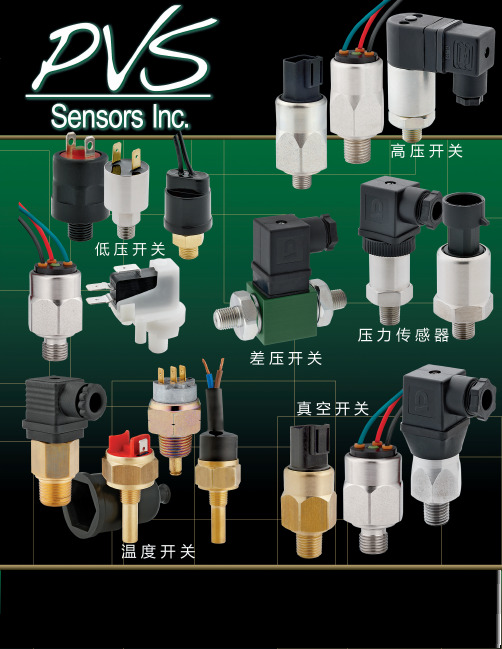
开关的保护:标准的PVS系列开关可以为绝大多数应用提供优质长寿命 的保护。开关具有防水保护,开关的浸润部分采用防腐材料构成,膜 片通常采用VITON® KAPTON®或EPDM膜片,能满足苛刻的行业应 用。外壳可选用钢铁,黄铜或不锈钢材质。
FTDATOWRFTTATINMOHWRALNOGARECELOGREUENCPTERAULILPSTOAAALNIPILOOANARNLCCANNR:ACCEEM:CSALSEEDM:ALEAS THREE PLACE
DO NOT S
PROHIBITED.
DO NOT SC
机械寿命: 1,000,000次
1 2 3
端子
公共端 常闭 常开
BPA FL CATALOG CUT AWAY A
接线
调压塞 上盖 密封圈
微动开关 顶杆
限位器 外壳
硅胶密封
调节头 弹簧 微动开关外壳
托盘 压盖 缓冲垫 膜片
BPA系列 结构示意图
上海办事处:18930221175 (江楠)Q:2244983398
3
Conv
MVA/MVF 真 空 开 关
.79 1.799.9 19.9
1.29 13.22.99 32.9
DIN型
Deutsch
TITLE:
2810 Blue RidgCe B29lv6d9.6 West Union, SC 29696
TIATALIIENN:PPTTCECEGGAARTRTAAAALLLLOODDGEGEUUATATCSCSSHSHYY
*不适用于 MPA/MVA
RTQ6050GF 高侧测量电流模拟芯片评估板评估板 EVB_RTQ6050GF-00 2023年5

High-Side Measurement Current-Shunt MonitorEvaluation BoardGeneral DescriptionThis document provides information on the function and use of the RTQ6050 evaluation board (EVB), as well as instructions for operating and modifying the board and circuit to meet individual requirements. Additionally, it includes details on the schematic diagram, bill of materials, and evaluation board layout.Table of ContentsGeneral Description (1)Performance Specification Summary (2)Power-up & Measurement Procedure (2)Detailed Description of Hardware (3)Bill of Materials (4)Typical Applications (5)Evaluation Board Layout (7)More Information (8)Important Notice for Richtek Evaluation Board (8)Performance Specification SummarySummary of the RTQ6050GF Evaluation Board performance specificiaiton is provided in Table 1. The ambient temperature is 25°C.Table 1. RTQ6050GF Evaluation Board Performance Specification SummaryDefault Input Voltage Default = 12V 2 -- 80 V Supply Voltage Default = 12V 2.9 -- 18 V Sensing Current -- 0.5 -- A Output Voltage -- 5 -- V Gain -- 20 -- V/V Gain Error -- -- ±2 % Offset Voltage, RTI -- ±0.5 ±2.5 mV Quiescent Current V OUT = 2V, T A = −40o C to 125o C -- -- 1200 μAPower-up & Measurement ProcedureSuggestion Required Equipments●RTQ6050GF Evaluation Board●DC Power Supply (Chroma, 62006P-100-25)●Electronic load capable of 6A●Function Generator●DC Meter●OscilloscopeQuick Start Procedures1. Apply VCC = 12V input power supply (2.9V < VCC < 18V) to VCC and GND terminals.2. Apply VIN+ = 12V input power supply (2V < VIN+ < 80V) to VIN+ and GND terminals.3. The default sense resistance is 100mΩ.4. Connect an external load to VIN- and GND terminals, and keep loading current = 0.5A.5. Measure the sense voltage (approximately 50mV) between VIN+ and VIN-.6. Measure the output voltage (approximately 1V) between VOUT and GND.Comparator Input, R3, and R4The RTQ6050 devices incorporate an open-drain comparator. This comparator typically has 1.3μs (typical) response time. The output of the comparator latches and is reset through the #RESET pin. The negative terminal is connected to a 0.6V internal reference, and the positive comparator input is connected to the CMPI pin of the device. Adjust R3 and R4 (show in EVB schematic) to set the comparator trip point for the intended application, where CMPI = (OUT × R4) / (R3 + R4) = 0.6V.Detailed Description of HardwareHeaders Description and PlacementCarefully inspect all the components used in the EVB according to the following Bill of Materials table, and then make sure all the components are undamaged and correctly installed. If there is any missing or damaged component, which may occur during transportation, please contact our distributors or e-mail us *************************.Test PointsThe EVB is provided with the test points and pin names listed in the table below.FunctionVCC Power input test point.OUT Output Voltage test point.CMPI Comparator input test point.GND Ground.#RESET Reset input pin.CMPO Open-drain comparator output.VIN- Negative current-sensing input.VIN+ Positive current-sensing input.JP1 VCC to ground test point.JP2 RESET jumper. Connect RESET to ground or pull high to VCC.SW1 RESET control switch. Connect RESET to ground or pull high to VCC.Bill of MaterialsC1, C2, C5 3 GRM188R71H104KA93D 0.1µF/25V/X7R/0603 Capacitor,Ceramic0603 MURATAR1, R2 2 RTT05000JTP 0/0805 Resistor 0805 RALEC R3, R4 2 RTT031001FTP 1k/0603 Resistor 0603 RALEC R5 1 WR06X1003FTL 100k/0603 Resistor 0603 WALSIN R6 1 RTT034701FTP 4.7k/0603 Resistor 0603 RALEC RSEN1 1 RTT25R100FTE 0.1 Resistor 2512 RALEC U1 1 RTQ6052GF RTQ6052GF CSOP MSOP-8 RICHTEKTypical ApplicationsEVB Schematic DiagramNote:1. Do not hot-plug input voltage and supply voltage on the boar. If hot-plugging is required, add ~100µF electrolyticcapacitor at the input.2. All the stated input and output capacitor values are the effective capacitances, including any de-rating effect, likea DC Bias. The stability of the converter may be impacted when using small size MLCC output capacitors, which may have much lower capacitance at the application DC output voltage than the rated value.TP1VCC 1GP1Power Supply 0V to 36VVIN-TP9GND 1TP10GND 1VCCTP3CMPI 1TP11GND1TP12GND1CMPITP5#RESET 1#RESETTP7VIN+1VIN+Test pinsTP8VIN-1TP6CMPO 1CMPOTP4GND 1TP2OUT 1OUTMeasurement Resultsand 0.6VCH1 = CMPICH2 = CMPOCH3 = #RESETEvaluation Board LayoutFigure 1. Top ViewFigure 2. Bottom ViewMore InformationFor more information, please find the related datasheet or application notes from Richtek website.Important Notice for Richtek Evaluation BoardTHIS DOCUMENT IS FOR REFERENCE ONLY, NOTHING CONTAINED IN THIS DOCUMENT SHALL BE CONSTRUED AS RICHTEK’S WARRANTY, EXPRESS OR IMPLIED, UNDER CONTRACT, TORT OR STATUTORY, WITH RESPECT TO THE PRESENTATION HEREIN. IN NO EVENT SHALL RICHTEK BE LIABLE TO BUYER OR USER FOR ANY AND ALL DAMAGES INCLUDING WITHOUT LIMITATION TO DIRECT, INDIRECT, SPECIAL, PUNITIVE OR CONSEQUENTIAL DAMAGES.。
sgs100a工作原理
sgs100a工作原理
SGS100A是一种高性能的半导体设备,常用于电力转换和控制系统。
这种设备的工作原理主要基于半导体物理和电气工程的理论。
以下是一些基本的原理和操作步骤:
1.半导体物理基础:SGS100A的核心是半导体材料,如硅或锗。
这些材料具有独特的电学特性,如导电性能可以被外部条件(如电压或温度)所改变。
2.p-n结:SGS100A的一个关键组成部分是p-n结,它是由两种不同类型的半导体(p型和n型)形成的界面。
在一定的电压作用下,p-n结内部的电荷分布会发生变化,从而产生电流。
3.操作步骤:SGS100A的操作通常包括三个步骤:整流、开关和逆变。
a. 整流:当外部交流电通过SGS100A的整流器时,整流器将交流电转换为直流电。
这是通过半导体p-n结的单向导电性实现的。
b. 开关:SGS100A的开关功能允许电流在两个方向中的任意一个中流动。
开关的开启和关闭是由半导体材料的导电性变化来控制的。
c. 逆变:当需要将直流电转换为交流电时,SGS100A使用逆变器将直流电转换为交流电。
这是通过半导体p-n结的双向导电性实现的。
4.应用:SGS100A在许多领域都有广泛的应用,如电力转换、电机控制、电源管理、UPS系统等。
它能够提高电力转换效率,降低能源消耗,同时具有体积小、重量轻、可靠性高等优点。
以上是对SGS100A的基本工作原理的简要说明。
需要注意的是,实际的工作过程可能会因具体的应用场景和设计参数而有所不同。
胎压计芯片说明书
SUNSTAR单片机专用电路/TEL:0755-********FAX:0755-********E-MAIL:**************胎压计芯片说明书一、 功能说明 (2)二、 原理图 (3)三、 I C脚位图 (4)四、 L C D图 (5)五、 邦定/标定测试架原理图 (6)六、 邦定、标定测试说明 (7)1/7SUNSTAR单片机专用电路/TEL:0755-********FAX:0755-********E-MAIL:**************一、 功能说明1. 工作电压:DC: 3.0V2. 工作电流:≤1000uA(不包括射灯和背光的电流)3. 静态电流: ≤5uA4. 开机LCD显示方式:三位半1.8.8.8或者三位8.8.85. 测量范围:3~150PSI;(可设置)6. 测量精度:1%FS7. 分辩率:0.5PSI 或0.1PSI(可选)8. 压力为零时显示:0.0PSI或00.0PSI;0 kpa或000kpa9. 工作温度:-10 至50度10.压力单位:PSI、BAR、KPA、KG/CM2(可选)11.单位保存:关机可保存单位,新上电不保存,默认单位可设置(无24C02)12.峰值锁定:显示压力值后10秒归零(归零时间可选)13.报警功能:超过最大压力显示“ERR”,可选择LCD闪或不闪14.低电提示:电池电压<2.5±0.15V低电符号闪烁或显示LO15.关机时间:20S关机(可选)16.背光时间:20S灭(可选按键开关或背光时间)。
当压力归零,然后再加气时如果背光灭,则可以选择重新开启背光17.射灯功能:射灯时间可选,通过按键开关。
18.按键功能:确认键(可单位切换,开关机,长按3秒进入预测值,关机和预测值功能只能同时选一项)、UP、DOWN键(进行预测值加减,可选长按3秒进入预测值)19.预测压力:3~100PSI循环(范围可设置)步进1.0PSI或0.5PSI20.蜂鸣器(可选):开机全显前或后响一声,按键音,小于预测值响3Bi,大于预测值响一声Bi(或者在±1P S I范围内响1Bi,不在范围闪3 Bi)可选同时LCD闪烁报警。
飞利浦 TP70i 胎压监测系统说明书
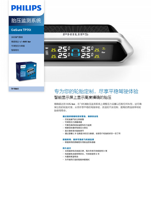
GoSure TP70i实时漏气警报精度高达 +/ -0.05 bar可调型压力阈值智能背光TP70IX1专为您的轮胎定制,尽享平稳驾驶体验智能显示屏上显示高度精确的胎压精确度达到 0.05 bar,在飞利浦胎压监测系统上调整压力设置以匹配任何车型。
这可确保出色的轮胎对准,从而尽享平稳的驾驶体验、改进的汽车控制、提高的燃油效率和轮胎使用寿命。
通过提供精确和实时警告,确保安全性在轮胎漏气时立即报警可调型压力测量阈值可靠性高的轮胎温度和压力监测根据您的喜好转换压力单位显示面板背光智能调节通过查看以 3 位数显示的压力数据,全部四个轮胎的状态一目了然即插即用,提供可靠的飞利浦品质即插即用的预编程车用级品质传感器持久运行太阳能供电无线显示屏,每次充电可持续使用 3 周传感器电池使用寿命长,可持续使用 5 年内置耐高温电池为节能而打造的智能休眠模式产品亮点实时漏气警报每年发生的交通事故中,很多都是因胎压过低导致摩擦过热爆炸、或因胎压过高直接引起爆炸。
为防止在驾驶过程中发生此类问题,胎压监测至关重要。
当轮胎漏气时,飞利浦 GoSure 胎压监测系统能够立即向您报警。
液晶显示屏上的警示灯可以准确地告诉您哪只轮胎需要补气。
可调型压力阈值飞利浦 GoSure TP 70i 胎压监测系统具有可调节的压力测量范围,可以对胎压和胎温进行监测。
精确的轮胎压力显示轮胎制造商建议用户定期检查胎压,然而很多驾驶员都是发现轮胎气压不足时才进行检查,但为时已晚。
轮胎看似充满气时,其实内部的压力可能已经大幅下降。
飞利浦 GoSure TP 70i 胎压监测系统能够以 +/-0.05 bar 的精度监测胎压,以 +/-3°C 的精度监测胎温。
精确的监测可防止您在轮胎气压不足的情况下驾驶,使得因漏气而造成意外发生降低三倍。
可转换压力单位在检查轮胎气压时,您是否遇到过这样的问题:车辆的用户手册上使用的压力单位是 bar ,但您的胎压显示屏上使用的单位却是 psi ,或者反之?飞利浦 GoSure TP 70i 胎压监测系统让您可以自主选择将压力单位,根据您的使用习惯,可以设置成 bar 或 psi 。
- 1、下载文档前请自行甄别文档内容的完整性,平台不提供额外的编辑、内容补充、找答案等附加服务。
- 2、"仅部分预览"的文档,不可在线预览部分如存在完整性等问题,可反馈申请退款(可完整预览的文档不适用该条件!)。
- 3、如文档侵犯您的权益,请联系客服反馈,我们会尽快为您处理(人工客服工作时间:9:00-18:30)。
QPS-100A胎压传感器芯片(PCB)
QPS-100A1胎压传感器芯片(PCB)系采用硅微机械加工技术制造,压阻原理。
本系列为绝对压力敏感芯片,采用各向异性腐蚀技术和硅硅直接键合技术在硅片内部形成一个长期
稳定的真空基准压力参考腔,在表面硅膜上用集成技术制作成惠斯顿应变检测全桥,从而在
受力时输出与压力成线性关系的电压信号。
一、产品应用领域
1:车载轮胎压力监测系统(TPMS产品);携带式胎压计、大气压力计。
2:悬挂、刹车、冷媒、进气管压力等汽车压力传感器。
3:压力OEM元件制造。
二、产品特点:
1:固态元件,三维集成MEMS工艺制造,可靠性高。
2:无应力设计与制造,严格自补偿浓度控制,稳定性好。
3:微型尺寸1mm×1mm×0.5mm,单元成本竞争力强。
4:使用方便,适合于任何陶瓷、PCB板、TO-8、塑胶微电子封装。
推荐采用1mA恒流供电,亦可采用5VDC恒压供电,建议供电电流不超过3mA
三、性能指标表:
性能指标单位备注
标准压力量程KPa 1500
最大过载能力%FS 300
输入输出阻抗KΩ 5±2
零位输出mV 0±40 1
满量程输出mV 100±40 1
线性度±%FS ≤±0.5 2
迟滞、重复性%FS ≤±0.1
未补偿零位温漂 ×10-4/℃.FS ≤±8 3
恒流供电灵敏度温漂 ×10-4/℃.FS ≤±5 3
恒压供电灵敏度温漂 ×10-4/℃.FS ≤-23 3
工作温度范围℃-40~125
四、接线定义(上图):
1为输入负电源(或地)端,
2为输出负信号端,
3右上角压焊点1为输入正电源端,
4左上角压焊点2为输出正信号端。
备注:1、5VDC恒压或1mA恒流供电下测得。
2、国家计量法规规定的最佳工作直线。
3、工作温区范围内任一个百度温区。
4、如无特别声明,测试环境条件均为25℃、5VDC、65%RH。
