BTA416Y-600C中文资料
BTA06-600C技术资料
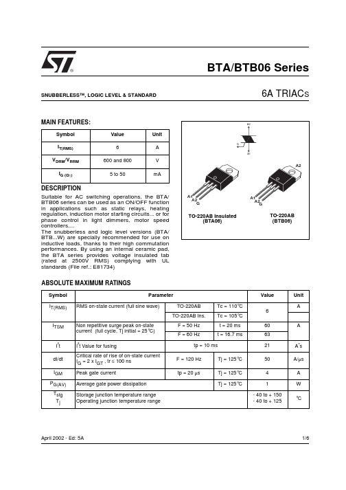
1/6®BTA/BTB06 SeriesSNUBBERLESS ™, LOGIC LEVEL & STANDARD6A TRIAC SApril 2002 - Ed: 5AMAIN FEATURES:DESCRIPTIONSuitable for AC switching operations, the BTA/BTB06 series can be used as an ON/OFF function in applications such as static relays, heating regulation, induction motor starting circuits... or for phase control in light dimmers, motor speed controllers,...The snubberless and logic level versions (BTA/BTB...W) are specially recommended for use on inductive loads, thanks to their high commutation performances. By using an internal ceramic pad,the BTA series provides voltage insulated tab (rated at 2500V RMS) complying with UL standards (File ref.: E81734)Symbol Value Unit I T(RMS)6A V DRM /V RRM600 and 800VI G (Q 1)5 to 50mAABSOLUTE MAXIMUM RATINGSSymbol ParameterValueUnit I T(RMS)RMS on-state current (full sine wave)TO-220ABTc = 110°C 6ATO-220AB Ins.Tc = 105°C I TSM Non repetitive surge peak on-state current (full cycle, Tj initial = 25°C) F = 50 Hz t = 20 ms 60AF = 60 Hzt = 16.7 ms63I ²t I ²t Value for fusingtp = 10 ms21A ²s dI/dt Critical rate of rise of on-state current I G = 2 x I GT , tr ≤ 100 ns F = 120 Hz Tj = 125°C 50A/µs I GM Peak gate currenttp = 20 µsTj = 125°C 4A P G(AV)Average gate power dissipation Tj = 125°C1W T stg T jStorage junction temperature range Operating junction temperature range- 40 to + 150- 40 to + 125°CBTA/BTB06 Series2/6ELECTRICAL CHARACTERISTICS (Tj = 25°C, unless otherwise specified)sSNUBBERLESS™ and LOGIC LEVEL (3 Quadrants)sSTANDARD (4 Quadrants)STATIC CHARACTERISTICSNote 1: minimum IGT is guaranted at 5% of IGT max.Note 2: for both polarities of A2 referenced to A1Symbol Test ConditionsQuadrantBTA/BTB06UnitTWSW CW BW I GT (1)V D = 12 V R L = 30 ΩI - II - III MAX.5103550mA V GT I - II - III MAX. 1.3V V GD V D = V DRM R L = 3.3 k ΩTj = 125°C I - II - IIIMIN.0.2V I H (2)I T = 100 mA MAX.10153550mA I L I G = 1.2 I GTI - III MAX.10255070mA II15306080dV/dt (2)V D = 67 %V DRM gate open Tj = 125°CMIN.20404001000V/µs (dI/dt)c (2)(dV/dt)c = 0.1 V/µs Tj = 125°C MIN.2.73.5--A/ms(dV/dt)c = 10 V/µs Tj = 125°C 1.2 2.4--Without snubber Tj = 125°C-- 3.55.3Symbol Test ConditionsQuadrant BTA/BTB06UnitCB I G (1)V D = 12 V R L = 30 ΩI - II - III IV MAX.255050100mA V GT ALL MAX. 1.3V V GD V D = V DRM R L = 3.3 k Ω Tj = 125°C ALLMIN.0.2V I H (2)I T = 500 mA MAX.2550mA I L I G = 1.2 I GTI - III - IVMAX.4050mA II80100dV/dt (2)V D = 67 %V DRM gate open Tj = 125°CMIN.200400V/µs (dV/dt)c (2)(dI/dt)c = 2.7 A/ms Tj = 125°CMIN.510V/µsSymbol Test ConditionsValue Unit V T (2)I TM = 5.5 A tp = 380 µs Tj = 25°C MAX. 1.55V V to (2)Threshold voltage Tj = 125°C MAX.0.85V R d (2)Dynamic resistance Tj = 125°C MAX.60m ΩI DRM I RRMV DRM = V RRMTj = 25°C MAX.5µA Tj = 125°C1mABTA/BTB06 Series3/6THERMAL RESISTANCESPRODUCT SELECTORBTB: non insulated TO-220AB packageORDERING INFORMATIONOTHER INFORMATIONNote: xxx = voltage, y = sensitivity, z = typeSymbol ParameterValue Unit R th(j-c)Junction to case (AC)TO-220AB 1.8°C/WTO-220AB Insulated 2.7R th(j-a)Junction to ambientTO-220ABTO-220AB Insulated60°C/W Part NumberVoltage (xxx)SensitivityType Package 600 V800 V BTA/BTB06-xxxB X X 50 mA Standard TO-220AB BTA/BTB06-xxxBW X X 50 mA Snubberless TO-220AB BTA/BTB06-xxxC X X 25 mA Standard TO-220AB BTA/BTB06-xxxCW X X 35 mA Snubberless TO-220AB BTA/BTB06-xxxSW X X 10 mA Logic level TO-220AB BTA/BTB06-xxxTWXX5 mALogic levelTO-220ABPart NumberMarkingWeight Base quantity Packing mode BTA/BTB06-xxxyz BTA/BTB06-xxxyz 2.3 g 250Bulk BTA/BTB06-xxxyzRGBTA/BTB06-xxxyz2.3 g50TubeBTA/BTB06 Series4/6Fig. 1: Maximum power dissipation versus RMS on-state current (full cycle).Fig. 2: RMS on-state current versus case temperature (full cycle).Fig. 3: Relative variation of thermal impedance versus pulse duration.Fig. 4: On-state characteristics (maximum values).Fig. 5: Surge peak on-state current versus number of cycles.Fig. 6: Non-repetitive surge peak on-state current for a sinusoidal pulse with width tp <10ms, and corresponding value of I²t.BTA/BTB06 Series5/6Fig. 7: Relative variation of gate trigger current,holding current and latching current versus junction temperature (typical values).Fig. 8-1: Relative variation of critical rate of decrease of main current versus (dV/dt)c (typical values). Snubberless & Logic Level T ypesFig. 8-2: Relative variation of critical rate of decrease of main current versus (dV/dt)c (typical values). Standard T ypesFig. 9: Relative variation of critical rate of decrease of main current versus junction temperature.BTA/BTB06 SeriesPACKAGE MECHANICAL DATAInformation furnished is believed to be accurate and reliable. However, STMicroelectronics assumes no responsibility for the consequences of use of such information nor for any infringement of patents or other rights of third parties which may result from its use. No license is granted by implication or otherwise under any patent or patent rights of STMicroelectronics. Specifications mentioned in this publication are subject to change without notice. This publication supersedes and replaces all information previously supplied. STMicroelectronics products are not authorized for use as critical components in life support devices or systems without express written approval of STMicroelectronics.© The ST logo is a registered trademark of STMicroelectronics© 2002 STMicroelectronics - Printed in Italy - All Rights ReservedSTMicroelectronics GROUP OF COMPANIESAustralia - Brazil - Canada - China - Finland - France - GermanyHong Kong - India - Isreal - Italy - Japan - Malaysia - Malta - Morocco - SingaporeSpain - Sweden - Switzerland - United Kingdom - United States.6/6。
bta08-600c可控硅参数
bta08-600c可控硅参数一、 bta08-600c可控硅的基本介绍bta08-600c是一种常用的可控硅器件,具有可控硅的常见特性,比如需要一定的触发电流和触发电压才能导通。
它广泛应用于各种电子设备和电路中,因此对其参数的深入了解和掌握对于电子工程师来说是非常重要的。
二、 bta08-600c可控硅的关键参数1. 触发电流和触发电压bta08-600c可控硅的触发电流和触发电压是其最基本的参数。
触发电流是指当外加触发电流大于该数值时,可控硅才能导通;而触发电压则是指当外加触发电压大于该数值时,可控硅才能导通。
这两个参数的大小直接影响到可控硅的导通性能,因此在实际电路设计中需要特别注意。
2. 典型电参数除了触发电流和触发电压外,bta08-600c可控硅的典型电参数还包括最大导通电流、最大反向电压、保持电流等。
这些参数的大小不仅影响了可控硅的工作性能,也直接关系到了其在电路中的安全性和稳定性。
3. 动态特性可控硅的动态特性是指其在导通和关断过程中的响应速度、响应时间等参数。
对于一些高频、高速电路来说,可控硅的动态特性显得尤为重要。
了解bta08-600c可控硅的动态特性,对于一些特定的电路设计来说具有重要的意义。
三、 bta08-600c可控硅的应用领域1. 电源电路在各种电源电路中,bta08-600c可控硅广泛应用于电压调节、开关控制等方面。
通过合理选择和使用可控硅,可以有效地提高电源电路的性能指标。
2. 照明电路在各种照明电路中,bta08-600c可控硅也扮演着重要的角色。
通过可控硅的控制,可以实现灯光的亮度调节、开关控制等功能。
3. 马达控制在各种马达控制电路中,bta08-600c可控硅同样发挥着重要的作用。
通过可控硅的控制,可以实现对马达的启动、停止、调速等功能。
四、 bta08-600c可控硅的个人观点和理解作为一种常见的可控硅器件,bta08-600c在电子领域有着广泛的应用。
BTA16-600C中文资料
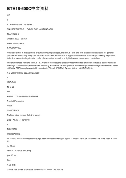
BTA16-600C中⽂资料1/7BTA/BTB16 and T16 SeriesSNUBBERLESS ? , LOGIC LEVEL & STANDARD16A TRIAC SOctober 2002 - Ed: 6AMAIN FEATURES:DESCRIPTIONAvailable either in through-hole or surface-mount packages, the BTA/BTB16 and T16 triac series is suitable for general purpose AC switching. They can be used as an ON/OFF function in applications such as static relays, heating regulation, induction motor starting circuits... or for phase control operation in light dimmers, motor speed controllers, ...The snubberless versions (BTA/BTB...W and T16series) are specially recommended for use on inductive loads, thanks to their high commutation performances. By using an internal ceramic pad,the BTA series provides voltage insulated tab (rated at 2500V RMS) complying with UL standards (File ref.: E81734).Symbol Value Unit I T(RMS)16A V DRM /V RRM 600, 700 and 800VI GT (Q 1)10 to 50mAABSOLUTE MAXIMUM RATINGSSymbol ParameterValueUnit I T(RMS)RMS on-state current (full sine wave)D22P AK Tc = 100°C 16ATO-220ABTO-220AB Ins.Tc = 85°C I TSM Non repetitive surge peak on-state current (full cycle, Tj initial = 25°C) F = 60 Hz t = 16.7 ms 168A F = 50 Hzt = 20 ms160I 2t I 2t Value for fusingtp = 10 ms144A 2s dI/dtCritical rate of rise of on-state current I G = 2 x I GT , tr ≤ 100 nsF = 120 Hz Tj = 125°C 50A/µs V DSM /V RSM Non repetitive surge peak off-statevoltagetp = 10 ms Tj = 25°C V DRM /V RRM+ 100V I GM Peak gate currenttp = 20 µsTj = 125°C 4A P G(AV)Average gate power dissipation Tj = 125°C1W T stg T jStorage junction temperature range Operating junction temperature range- 40 to + 150- 40 to + 125°CBTA/BTB16 and T16 Series2/7ELECTRICAL CHARACTERISTICS (Tj = 25°C, unless otherwise specified)sSNUBBERLESS? and LOGIC LEVEL (3 Quadrants)sSTANDARD (4 Quadrants)STATIC CHARACTERISTICSNote 1: minimum IGT is guaranted at 5% of IGT max.Note 2: for both polarities of A2 referenced to A1 Symbol Test ConditionsQuadrantT16BTA/BTB16UnitT1635SW CW BW I GT (1)V D = 12 V R L = 33 ?I - II - III MAX.35103550mA V GT I - II - III MAX. 1.3V V GD V D = V DRM R L = 3.3 k ? Tj = 125°C I - II - IIIMIN.0.2V I H (2)I T = 500 mA MAX.35153550mA I L I G = 1.2 I GTI - III MAX.50255070mA II60306080dV/dt (2)V D = 67 % V DRM gate open Tj = 125°C MIN.500405001000V/µs (dI/dt)c (2)(dV/dt)c = 0.1 V/µs Tj = 125°CMIN.-8.5--A/ms(dV/dt)c = 10 V/µs Tj = 125°C - 3.0--Without snubber Tj = 125°C8.5-8.514Symbol Test ConditionsQuadrant BTA/BTB16UnitCB I GT (1)V D = 12 V R L = 33 ?I - II - III IV MAX.255050100mA V GT ALL MAX. 1.3V V GD V D = V DRM R L = 3.3 k ? Tj = 125°C ALLMIN.0.2V I H (2)I T = 500 mA MAX.2550mA I L I G = 1.2 I GTI - III - IVMAX.4060mA II80120dV/dt (2)V D = 67 % V DRM gate open Tj = 125°CMIN.200400V/µs (dV/dt)c(2)(dI/dt)c = 7 A/ms Tj = 125°CMIN.510V/µsSymbol Test ConditionsValue Unit V TM (2)I TM = 22.5 A tp = 380 µs Tj = 25°C MAX. 1.55V V to (2)Threshold voltage Tj = 125°C MAX.0.85V R d (2)Dynamic resistance Tj = 125°C MAX.25m ?I DRM I RRMV DRM = V RRMTj = 25°C MAX.5µA Tj = 125°C2mABTA/BTB16 and T16 Series3/7THERMAL RESISTANCESS: Copper surface under tabPRODUCT SELECTORORDERING INFORMATIONSymbol ParameterValue Unit R th(j-c)Junction to case (AC)D 2PAK TO-220AB 1.2°C/WTO-220AB Insulated2.1R th(j-a)Junction to ambientS = 1 cm 2D 2PAK 45°C/WTO-220AB 60TO-220AB InsulatedPart NumberVoltage(xxx)SensitivityTypePackage600 V700 V 800 V BTA/BTB16-xxxB X X X 50 mA Standard TO-220AB BTA/BTB16-xxxBW X X X 50 mA Snubberless TO-220AB BTA/BTB16-xxxC X X X 25 mA Standard TO-220AB BTA/BTB16-xxxCW X X X 35 mA Snubberless TO-220ABBTA/BTB16-xxxSW X XX 10 mA Logic level TO-220AB T1635-xxxGXX35 mASnubberlessD 2PAKBTA/BTB16 and T16 Series4/7OTHER INFORMATIONNote: xxx = voltage, y = sensitivity, z = typePart NumberMarkingWeight Base quantity Packing mode BTA/BTB16-xxxyz BTA/BTB16xxxyz 2.3 g 250Bulk BTA/BTB16-xxxyzRG BTA/BTB16-xxxyz 2.3 g 50Tube T1635-xxxG T1635xxxG 1.5 g 50Tube T1635-xxxG-TRT1635xxxG1.5 g1000T ape & reelFig. 1: Maximum power dissipation versus RMS on-state current (full cycle).Fig. 2-1: RMS on-state current versus case temperature (full cycle).Fig. 2-2: D2PAK RMS on-state current versus ambient temperature (printed circuit board FR4,copper thickness: 35µm), full cycle.Fig. 3: Relative variation of thermal impedance versus pulse duration.BTA/BTB16 and T16 Series5/7Fig. 4: On-state characteristics (maximum values)Fig. 5: Surge peak on-state current versus number of cycles.Fig. 6: Non-repetitive surge peak on-state current for a sinusoidal pulse with width tp <10ms, and corresponding value of I2t. Fig. 7: Relative variation of gate trigger current,holding current and latching current versus junction temperature (typical values).Fig. 8: Relative variation of critical rate of decrease of main current versus (dV/dt)c (typical values).Fig. 9: Relative variation of critical rate of decrease of main current versus junction temperature.BTA/BTB16 and T16 SeriesFig. 10:D2P AK Thermal resistance junction to ambient versus copper surface under tab (printed circuit board FR4, copperthickness: 35µm).PACKAGE MECHANICAL DATA6/7BTA/BTB16 and T16 Series PACKAGE MECHANICAL DATAFOOTPRINT DIMENSIONS (in millimeters)Information furnished is believed to be accurate and reliable. However, STMicroelectronics assumes no responsibility for the consequences of use of such information nor for any infringement of patents or other rights of third parties which may result from its use. No license is granted by implication or otherwise under any patent or patent rights of STMicroelectronics. Specifications mentioned in this publication are subject to change without notice. This publication supersedes and replaces all information previously supplied. STMicroelectronics products are not authorized for use as critical components in life support devices or systems without express written approval of STMicroelectronics.The ST logo is a registered trademark of STMicroelectronics2002 STMicroelectronics - Printed in Italy - All Rights ReservedSTMicroelectronics GROUP OF COMPANIESAustralia - Brazil - Canada - China - Finland - France - GermanyHong Kong - India - Isreal - Italy - Japan - Malaysia - Malta - Morocco - SingaporeSpain - Sweden - Switzerland - United Kingdom - United States./doc/b7997dde195f312b3169a58b.html7/7。
BTA416Y-800C中文资料

103 ITSM (A)
(1)
003aab818
102
IT
ITSM
t
tp
Tj(init) = 25 °C max
10 10-5
10-4
10-3
10-2
10-1
tp (s)
© NXP B.V. 2007. All rights reserved.
4 of 12
元器件交易网
NXP Semiconductors
BTA416Y series B and C
16 A 3-quadrant triacs, insulated, high commutation, high temperature
IGM PGM PG(AV) Tstg Tj
rate of rise of on-state current
peak gate current peak gate power average gate power storage temperature junction temper = 0.2 A; dIG/dt = 0.2 A/µs
3. Ordering information
Table 2. Ordering information
Type number
Package
Name
Description
Version
BTA416Y-600B BTA416Y-600C
TO-220
plastic single-ended package; isolated heatsink mounted; 1 mounting hole; SOT78D 3-lead TO-220
BTA41-700B中文资料

BTA41A/B BTB41BMarch 1995STANDARD TRIACSSymbol ParameterValue Unit I T(RMS)RMS on-state current (360°conduction angle)BTA Tc =75°C 40ABTBTc =85°C 45I TSMNon repetitive surge peak on-state current (Tj initial =25°C )tp =8.3ms 315A tp =10ms 300I 2t I 2t valuetp =10ms 450A 2s dI/dtCritical rate of rise of on-state currentGate supply :I G =500mA di G /dt =1A/µsRepetitive F =50Hz 10A/µs Non Repetitive50Tstg Tj Storage and operating junction temperature range-40to +150-40to +125°C °C TlMaximum lead temperature for soldering during 10s at 4.5mm from case260°C TOP 3(Plastic)A1A2G.HIGH SURGE CURRENT CAPABILITY .COMMUTATION :(dV/dt)c >10V/µs .BTA Family :INSULATING VOLTAGE =2500V (RMS)(UL RECOGNIZED :E81734)DESCRIPTIONSymbol ParameterBTA41-...A/B /BTB41-...BUnit400600700800V DRM V RRM Repetitive peak off-state voltage Tj =125°C400600700800VABSOLUTE RATINGS (limiting values)FEATURESThe BTA41A/B /BTB41B triac family are high performance glass passivated PNPN devices.These parts are suitables for general purpose ap-plications where high surge current capability is re-quired.Application such as phase control and static switching on inductive or resistive load.1/5GATE CHARACTERISTICS (maximum values)Symbol ParameterValue Unit Rth (j-a)Junction to ambient50°C/W Rth (j-c )DC Junction to case for DCBTA 1.2°C/WBTB0.8Rth (j-c)AC Junction to case for 360°conduction angle(F=50Hz)BTA 0.9°C/W BTB0.6SymbolTest ConditionsQuadrantSuffixUnitAB I GTV D =12V(DC)R L =33ΩTj=25°CI-II-III MAX 10050mA IVMAX 150100V GT V D =12V(DC)R L =33ΩTj=25°C I-II-III-IV MAX 1.5V V GD V D =V DRM R L =3.3k ΩTj=125°C I-II-III-IV MIN 0.2V tgt V D =V DRM I G =500mA dI G /dt =3A/µs Tj=25°C I-II-III-IV TYP 2.5µs I LI G =1.2I GTTj=25°CI-III-IV TYP7060mA II200180I H *I T =500mA gate open Tj=25°C MAX 10080mA V TM *I TM =60A tp=380µs Tj=25°C MAX 1.8V I DRM I RRM V DRM Rated V RRMRatedTj=25°C MAX 0.01mATj=125°C MAX 6dV/dt *Linear slope up to V D =67%V DRM gate open Tj=125°CMIN250250V/µs(dV/dt)c *(dI/dt)c =18A/ms BTA (dI/dt)c =20A/msBTBTj=125°C MIN 10V/µs*For either polarity of electrode A 2voltage with reference to electrode A 1.P G (AV)=1WP GM =40W (tp =20µs)I GM =8A (tp =20µs)V GM =16V (tp =20µs).ELECTRICAL CHARACTERISTICSTHERMAL RESISTANCESBTA41A/B /BTB41B2/5ORDERING INFORMATIONPackage I T(RMS)V DRM/V RRM Sensitivity SpecificationA V A BBTA (Insulated)41400X X600X X700X X800X XBTB (Uninsulated)45400X600X700X800XFig.1:Maximum RMS power dissipation versus RMS on-state current(F=50Hz).(Curves are cut off by(dI/dt)c limitation)(BTA)Fig.2:Correlation between maximum RMS power dissipation and maximum allowable temperatures(T amb and T case)for different thermal resistances heatsink+ contact(BTA).Fig.3:Maximum RMS power dissipation versus RMS on-state current(F=50Hz).(Curves are cut off by(dI/dt)c limitation)(BTB)Fig.4:Correlation between maximum RMS power dissipation and maximum allowable temperatures(T amb and T case)for different thermal resistances heatsink+ contact(BTB).BTA41A/B/BTB41B3/5Fig.8:Relative variation of gate trigger current and holding current versus junction temperature.Fig.9:Non Repetitive surge peak on-state current versus number of cycles.Fig.10:Non repetitive surge peak on-state current for a sinusoidal pulse with width :t ≤ 10ms,and corresponding value of I 2t.1E-31E-21E-11E+01E+11E+21E+30.010.101.00Zth/Rth Zth(j-c)Zth(j-a)tp(s)Fig.7:Relative variation of thermal transient impedance pulse duration.Fig.5:RMS on-state current versus case temperature.(BTA)Fig.6:RMS on-state current versus case temperature.(BTB)BTA41A/B /BTB41B4/5Fig.11:On-state characteristics (maximum values).PACKAGE MECHANICAL DATA TOP 3PlasticCooling method :C Marking :type number Weight :4.7gRecommended torque value :0.8m.N.Maximum torqur value :1m.N.HR 4.6CAGDBPN NL MJIREF.DIMENSIONSMillimeters Inches Min.Max.Min.Max.A 15.1015.500.5940.611B20.7021.100.8140.831C 14.3015.600.5610.615D 16.1016.500.6320.650G 3.40-0.133-H 4.40 4.600.1730.182I 4.08 4.170.1610.164J1.45 1.550.0570.062L 0.500.700.0190.028M2.70 2.900.1060.115N 5.40 5.650.2120.223P1.201.400.0470.056Information furnished is believed to be accurate and reliable.However,SGS-THOMSON Microelectronics assumes no responsability for the consequences of use of such information nor for any infringement of patents or other rights of third parties which may result from its use.No license is granted by implication or otherwise under any patent or patent rights of SGS-THOMSON Microelectronics.Specifications mentioned in this publication are subject to change without notice.This publication supersedes and replaces all information previously supplied.SGS-THOMSON Microelectronics products are not authorized for use as critical components in life support devices or systems without express written approval of SGS-THOMSON Microelectronics.©1995SGS-THOMSON Microelectronics -Printed in Italy -All rights reserved.SGS-THOMSON Microelectronics GROUP OF COMPANIESAustralia -Brazil -France -Germany -Hong Kong -Italy -Japan -Korea -Malaysia -Malta -Morocco -The Nether-lands -Singapore -Spain -Sweden -Switzerland -Taiwan -Thailand -United Kingdom -U.S.A.BTA41A/B /BTB41B5/5。
BTA41A中文资料
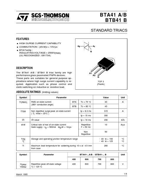
Fig.7 : Relative variation of thermal transient impedance pulse duration.
Fig.8 : Relative variation of gate trigger current and holding current versus junction temperature.
Symbol Rth (j-a) Junction to ambient BTA BTB Rth (j-c) AC Junction to case for 360° conduction angle ( F= 50 Hz) BTA BTB Parameter Value 50 1.2 0.8 0.9 0.6 °C/W Unit °C/W °C/W
Symbol IT(RMS) RMS on-state current (360° conduction angle) Non repetitive surge peak on-state current ( Tj initial = 25°C ) I2t value Critical rate of rise of on-state current Gate supply : IG = 500mA diG/dt = 1A/µs Parameter BTA BTB Tc = 75 °C Tc = 85 °C tp = 8.3 ms tp = 10 ms tp = 10 ms Repetitive F = 50 Hz Non Repetitive Tstg Tj Tl Storage and operating junction temperature range Maximum lead temperature for soldering during 10 s at 4.5 mm from case Parameter 400 VDRM VRRM Repetitive peak off-state voltage Tj = 125 °C 400 Value 40 45 315 300 450 10 50 - 40 to + 150 - 40 to + 125 260 °C °C °C A2s A/µs A Unit A
BTA16-600BW3G;BTA16-800BW3G;中文规格书,Datasheet资料

TJ
−40 to +125 °C
Storage Temperature Range
Tstg −40 to +150 °C
RMS Isolation Voltage (t = 300 ms, R.H. ≤ 30%, TA = 25°C)
Viso
2500
V
Stresses exceeding Maximum Ratings may damage the device. Maximum Ratings are stress ratings only. Functional operation above the Recommended Operating Conditions is not implied. Extended exposure to stresses above the Recommended Operating Conditions may affect device reliability. 1. VDRM and VRRM for all types can be applied on a continuous basis. Blocking
/
3
TC, CASE TEMPERATURE (°C)
− MT2 NEGATIVE (Negative Half Cycle)
All polarities are referenced to MT1. With in−phase signals (using standard AC lines) quadrants I and III are used.
+
(+) MT2
(+) MT2
Quadrant II IGT −
BTA40,BTA41,BTB4-可控硅 中文自翻资料
8
门极平均耗散功率 PG(AV) Average gate power dissipation
Tj = 125 °C
1
Tstg
Storage junction temperature range 储存温度
Tj
Operating junction temperature range 有效结温
- 40 to + 150 - 40 to + 125
Parameter 参数
I - II - III IV ALL
MAX. MAX.
Value 值
50 100 1.3
控制极不触发电压
VGD
VD = VDRM RL = 3.3 kΩ Tj = 125 °C
ALL
MIN.
0.2
维持电流
IH (2)
IT = 500 mA
MAX.
80
擎住电流
IL
IG = 1.2 IGT
MAX. MAX. MAX.
MAX.
Table 5.表4 Thermal resistance 热阻
符号 Symbol
Test conditions 试验条件
Rth(j-c) Rth(j-a)
Junction to case (AC) 结至壳体
Junction to ambient 结至环境
RD91 (insulated) / TOP3 insulated TOP3 TOP3 / TOP3 insulated
I - III - IV II
70 MAX.
160
断态电压临界上升率 dV/dt(2) 注2 VD = 67% VDRM gate open (dV/dt)c(2)注2 (dI/dt)c = 20 A/ms
瑞能半导体产品指南说明书

PRODUCT SELECTION GUIDEWeEn SemiconductorsEV CHARGERTELECOM POWERSOLAR INVERTERHOME APPLIANCEMOTOR CONTROL瑞能半导体科技股份有限公司,源自恩智浦半导体标准产品事业部,注册于 2015年8月5号,运营中心落户上海,全资子公司和分支机构包括吉林芯片生产基地、上海和英国产品及研发中心、香港物流中心以及遍布全球其他国家的销售和客户服务点。
作为全球功率半导体行业的佼佼者,瑞能始终专注于研发行业领先、广泛且深入的双极功率半导体产品组合,包括:碳化硅二极管,可控硅整流器和三端双向可控硅、功率二极管、高压晶体管等。
产品广泛应用于电信、计算机、消费类电子产品、智能家电、照明、汽车和电源管理应用等市场领域。
自诞生以来,瑞能已走过逾 50 年辉煌历程,我们的目标是帮助客户提高成本效益和生产效率,促进中国及全球智能制造行业的发展。
19691980s2000s20062020201520132009High Voltage Transistors (HVT)Fast, Ultrafast & Hyperfast Power DiodesBipolar 4-Quadrant TriacsBipolar 3-Quadrant Hi-Com TriacsHyperfast diodes Triac & SCR Planar Technology PlatformACT & ACTT Platform (AC Switch), Casco DiodesTemperature & Overload Protected Triac (TOPTriac)Automotive SiC Standard Power Diodes Automotive SCRs 1600V Planar SCRsSilicon Carbide DiodesEnhanced E ciency Pt Planar diodes (EEPP)Generation 2: Schottky Barrier Diodes High Voltage SCRsSuper Advanced Best E ciency Rectifier Diodes (SABER)Generation 1: Schottky Barrier DiodesWeEn Semiconductors:A Spin-o Company from NXP;Over 50-Y ears Leading Experience in PowerWeEn Semiconductors Co., Ltd, span o from NXP, registered on Aug 5, 2015 .The operational headquarters locates in Shanghai and the company’s wholly-owned subsidiaries and branches include: the front-end fabrication in Jilin, north east China, research & development centers in Shanghai and Manchester, UK, and the warehouse and distribution center in Hong Kong. WeEn also has sales o ces set up and customer service access throughout the world.As a key player in the semiconductor industry, WeEn has focused on developing a large portfolio of industry-leading bipolar power products including silicon carbide diode, thyristors (i.e. silicon controlled rectifiers and triacs), silicon power diodes and high voltage transistors etc. All these products are widely used in the markets for telecommunications, computers, consumer electronics, intelligent home appliances, lighting, automotive and power management applications.With over 50 years of design and manufacture experience, the aim of WeEn is to help our customers achieve higher cost e ciency and production e ciency and to contribute to the development of China and global intelligent manufacturing.AC Thyristor Triacs / AC ThyristorsAC Thyristor TriacsAC ThyristorsTemperature and Overload Protected Triacs (Toptriac)3Q Hi-com Triacs (0.8A - 45A)4Q Triacs (0.6A - 45A)Silicon Controlled Rectifiers (0.8A - 126A)Power DiodesHyperfast Power Diodes1200V Planar Hyperfast Power DiodesPower DiodesUltrafast Power DiodesSiC Schottky DiodePower Schottky Diodes600V - 1600V Standard Power DiodesPower Diode BridgePower Diode ModuleWeEn High Voltage 1600V SCRs1600V/50A & 1600V/80A, Planar PassivatedWeEn 30A Hi-Com TM TriacsDFN 8x8 PackageWeEn Silicon Carbide Junction Barrier Schottky (JBS) 650V and 1200V SeriesWeEn Products for EV On Board ChargerWeEn Products in Smart HomeCertificationsWeEn Nanchang Reliability & Failure Analysis Laboratory 040506070809101112131415161718193Contents(3Q Hi-Com power switches, overvoltage protection)AC Thyristor Triacs / AC ThyristorsAC Thyristor TriacsTemperature and Overload Protected Triacs (Toptriac)2Q Hi-Com power switches, exclusive negative gate triggering, over-temperature protectionAC Thyristor Triacs part numbering AC Thyristors part numbering(2Q Hi-Com power switches, exclusive negative gate triggering, ’Common’ mounting base, overvoltage protection)AC ThyristorsI GT key: C = 35 mA; C0 = 5 - 30 mA; E = 10 mAT : high T j (max) 150 °C N: Enhanced Dynamic PerformanceI GT key: D = 5 mA; E = 10 mAI GT key:C0 = 5 - 35mATypes in bold red italic represent products in development4Types in bold red represent new productsHi-Com Triacs (0.8A - 45A)3Q5I key:* High I TSM **: Enhanced immunity to false triggering T: high T j (max) 150CD = 5mA (10mA in 3+);E = 10mA (25mA in 3+);F = 25mA (70mA in 3+); - = 35mA (70mA in 3+);G = 50mA (100mA in 3+); G0 = 50mA (100mA in 3+), 10mA min4Q Triacs(0.6A - 45A)4Q Triacs part numbering6Silicon Controlled Rectifiers(0.8A - 126A)Silicon Controlled Rectifiers part numberinghigh I TSM ** Hi-Com / fast turn-off T: high T j (max) 150 A: Automotive quali ed AEC-Q101°CTypes in bold red represent new productsTypes in bold red italic represent products in development7Hyperfast Power Diodes1200V Planar Hyperfast Power DiodesTypes in bold red represent new productsTypes in bold red italic represent products in development8Types in bold red italic represent products in development9SOD113(2-pin SOT186A)SOT429(3-pin TO247)NXPSC04650X NXPSC06650X SiC Schottky Diode650V SiC Schottky Diode• Highly stable switching performance • High forward surge capability IFSM • Extremely fast reverse recovery time• Superior in ef ciency to Silicon Diode alternatives • Reduced losses in associated MOSFET • Reduced EMI• Reduced cooling requirements • RoHS compliantI n t h e S p o t l i g h t Types in bold red italic represent products in development1200V SiC Schottky Diode• Highly stable switching performance • High forward surge capability IFSM • Extremely fast reverse recovery time• Superior in ef ciency to Silicon Diode alternatives • Reduced losses in associated MOSFET • Reduced EMI• Reduced cooling requirements • RoHS compliant• High junction operating temperature capability (T j(max) = 175 °C)I n t h e S p o t l i g h t10Power Schottky Diodes600V - 1600V Standard Power DiodesPower Diode Moduleemploying series die technology for the lowest possible trrWDMF75M16• Three phase recti ers• Heat transfer through aluminium oxide DBC, ceramic isolated metal baseplate • High voltage capability• High inrush current capability • Planar process• High operating temperature capability (T j (max) = 150°C)I n t h e S p o t l i g h tPower Diode BridgeTypes in bold red represent new productsWDMF75M1611WeEn High Voltage 1600V SCRs1600V/50A & 1600V/80A, Planar PassivatedProductTYN50W-1600T TYN80W-1600T TO-247TO-247Key ParametersPackageParametersPackageIT(AV)IT(RMS)VDRMIGTITSMTj(max)dIT/dtdVD/dtTO-24750A79A1600V80mA max650A @ 10ms150°C150A/us1500V/µs @150o CTYN50W-1600TTO-24780A126A1600V80mA max850A @ 10ms150°C150A/us1000V/µs @150o CTYN80W-1600TProduct 12WeEn 30A Hi-Com TM TriacsProductApplications PackageParametersI T(RMS)V DRM I GT I TSM T j(max)dI T /dt30A 800V 50mA max 270A @ 20ms 150°C 100A/µsBTA330 BT series30A 800V 35mA max 270A @ 20ms 150°C 100A/µsBTA330 CT seriesBTA330-800BT BTA330X-800BT BTA330Y-800BT BTA330Y-800CT BTA330B-800BT BTA330B-800CTTO220TO220FP IITO220IITO220D 2PAK D PAKKey ParametersProduct13DFN 8x8 PackagePackage OutlinePart NoV DC(V)I F (A)V F (V)*1I FSM (A)*2Cd(pF)*3I R (mA)L x W x H (mm 3)WNSC04650T WNSC06650T WNSC08650T WNSC10650T650650650650468101.561.501.551.5836547276468101.561.501.551.5810 x 11 x 4.41104848 x 8 x 0.856454.4-42%-88%Footprint (mm 2)Volume (mm 3)D 2PAK Telecom / Server power Photovoltaic inverterDFN 8X8DFN 8X8 vs D 2PAK1415WeEn SiC JBS for Photovoltaic InverterWeEn Silicon Carbide Junction Barrier Schottky (JBS) 650V and 1200V SeriesKey features of WeEn SiC JBS· No reverse recovery charge · Qr temperature independent · High thermal conductivityNXPSC10650NXPSC20650WeEn SiC JBS for Server Power / Telecom Power D2,D3: SiCNXPSC20650W NXPSC10650XVoltage650V 1200VCurrent4-30A 2-40APackageTO220 / TO247 / DPAK / D 2PAK TO220 / TO247NXPSC20650W-A BT155W-1200T-A BT153B-1200T-A BYC30W-600PT2-AWeEn Products for EV On Board Charger16Automotive Grade, AEC-Q101 qualified· Fast Switching Silicon Diodes T j(max) 175°C · High E ciency Silicon Carbide Diodes T j(max) 175°C · High Current SCRs T j(max) 150°CWeEn Products in Smart HomeDish Washer· Planar passivated ACT/ACTT series with over-voltage clamp function· ACT108W-800E used for water inlet valve control · ACTT4S-800E used for water extraction pump controlWash Machine· Planar Passivated technology with the best false trigger capability· BTA201W-800E used for Valve control · BTA416Y-800C used for drum motor controlAir-con· Platinum-doping SABER TM Series Fast Recovery Diodes· BYV415W-600P, BYV415J-600P used for PFC · BYV30JT-600P, BYC30W-600PT2, BYC20X-600P, BYC30X-600P used for traditional PFCCoffee Machine:· Planar passivated technology, high T j(max) 150o C capability for better heating control· BTA316Y-800CT used for heating element control · TOPT16-800C0 used for heating element control with over temp. protection function embedded17Certifications18Items of Reliability test & FAWeEn Nanchang Reliability & Failure Analysis Laboratory瑞能南昌可靠性测试实验室及失效分析实验室F I B &S E M&E D XX -R A Y T e s e c C -S A MT e m p e r atu r e C y c l eU H A S T &PP O TR e v e r s e bia s t r o p i ca lE S D (H B M&M M )Website: Mailbox:********************2020 WeEn SemiconductorsAll rights reserved. Reproduction in whole or in part is prohibited without the prior written consent of the copyright owner. Theinformation presented in this document does not form part of any quotation or contract, is believed to be accurate and reliable and may be changed without notice. No liability will be accepted by the publisher for any consequence of its use. Publication thereof does not convey nor imply any license under patent- or other industrial or intellectual property rights.Date of release: July 2020Document order number: 20200701。
BTA216X-600D中文资料

Philips Semiconductors Objective specificationThree quadrant triacs BTA216X series D, E and Fguaranteed commutationGENERAL DESCRIPTIONQUICK REFERENCE DATAPassivated guaranteed commutation SYMBOLPARAMETERMAX.MAX.UNITtriacs in a full pack,plastic envelope intended for use in motor control circuits BTA216X-600D -or with other highly inductive loads.BTA216X-600E 800E These devices balance the BTA216X-600F 800F requirements of commutation V DRM Repetitive peak off-state 600800V performance and gate sensitivity.The voltages"sensitive gate"E series and "logic level"I T(RMS)RMS on-state current1616A D series are intended for interfacing with I TSMNon-repetitive peak on-state 140140Alow power drivers,including micro currentcontrollers.PINNING - SOT186APIN CONFIGURATIONSYMBOLLIMITING VALUESLimiting values in accordance with the Absolute Maximum System (IEC 134).SYMBOL PARAMETERCONDITIONSMIN.MAX.UNIT -600-800V DRM Repetitive peak off-state -6001800V voltagesI T(RMS)RMS on-state current full sine wave;-16AT hs ≤ 38 ˚C I TSMNon-repetitive peak full sine wave;on-state currentT j = 25 ˚C prior to surge t = 20 ms -140A t = 16.7 ms -150A I 2t I 2t for fusingt = 10 ms-98A 2s dI T /dt Repetitive rate of rise of I TM = 20 A; I G = 0.2 A;100A/µs on-state current after dI G /dt = 0.2 A/µs triggeringI GM Peak gate current -2A V GM Peak gate voltage -5V P GM Peak gate power -5W P G(AV)Average gate power over any 20 ms -0.5W periodT stg Storage temperature -40150˚C T jOperating junction -125˚Ctemperature1 Although not recommended, off-state voltages up to 800V may be applied without damage, but the triac may switch to the on-state. The rate of rise of current should not exceed 15 A/µs.Philips Semiconductors Objective specification Three quadrant triacs BTA216X series D, E and F guaranteed commutationISOLATION LIMITING VALUE & CHARACTERISTICThs= 25 ˚C unless otherwise specifiedSYMBOL PARAMETER CONDITIONS MIN.TYP.MAX.UNITVisol R.M.S. isolation voltage from all f = 50-60 Hz; sinusoidal--2500V three terminals to external waveform;heatsink R.H. ≤ 65% ; clean and dustfreeCisol Capacitance from T2 to external f = 1 MHz-10-pF heatsinkTHERMAL RESISTANCESSYMBOL PARAMETER CONDITIONS MIN.TYP.MAX.UNITRth j-hs Thermal resistance full or half cyclejunction to heatsink with heatsink compound-- 4.0K/Wwithout heatsink compound-- 5.5K/WRth j-a Thermal resistance in free air-55-K/W junction to ambientSTATIC CHARACTERISTICSTj= 25 ˚C unless otherwise statedSYMBOL PARAMETER CONDITIONS MIN.TYP.MAX.UNITBTA216X-...D...E...FI GT Gate trigger current2VD= 12 V; IT= 0.1 AT2+ G+--51025mAT2+ G---51025mAT2- G---51025mAI L Latching current VD= 12 V; IGT= 0.1 AT2+ G+--152025mAT2+ G---253040mAT2- G---253040mAI H Holding current VD= 12 V; IGT= 0.1 A--152530mAVT On-state voltage IT= 20 A- 1.2 1.5VVGT Gate trigger voltage VD= 12 V; IT= 0.1 A-0.7 1.5VVD= 400 V; IT= 0.1 A;0.250.4-VTj= 125 ˚CI D Off-state leakage current VD= VDRM(max);-0.10.5mATj= 125 ˚C2 Device does not trigger in the T2-, G+ quadrant.Philips Semiconductors Objective specificationThree quadrant triacs BTA216X series D, E and Fguaranteed commutationDYNAMIC CHARACTERISTICST j = 25 ˚C unless otherwise stated SYMBOL PARAMETER CONDITIONSMIN.TYP.MAX.UNIT BTA216X-...D ...E ...F dV D /dtCritical rate of rise of V DM = 67% V DRM(max);306070--V/µsoff-state voltage T j = 110 ˚C; exponential waveform; gate open circuitdI com /dtCritical rate of change of V DM = 400 V; T j = 110 ˚C; 1.8 3.5 4.5--A/mscommutating currentI T(RMS) = 16 A;dV com /dt = 20v/µs; gate open circuitdI com /dtCritical rate of change of V DM = 400 V; T j = 110 ˚C; 4.3 5.3 6.3--A/mscommutating currentI T(RMS) = 16 A;dV com /dt = 0.1v/µs; gate open circuitt gtGate controlled turn-on I TM = 20 A; V D = V DRM(max);---2-µstimeI G = 0.1 A; dI G /dt = 5 A/µsPhilips Semiconductors Objective specificationThree quadrant triacs BTA216X series D, E and Fguaranteed commutationMECHANICAL DATA1. Refer to mounting instructions for F-pack envelopes.2. Epoxy meets UL94 V0 at 1/8".Philips Semiconductors Objective specification Three quadrant triacs BTA216X series D, E and F guaranteed commutationDEFINITIONSData sheet statusObjective specification This data sheet contains target or goal specifications for product development. Preliminary specification This data sheet contains preliminary data; supplementary data may be published later. Product specification This data sheet contains final product specifications.Limiting valuesLimiting values are given in accordance with the Absolute Maximum Rating System (IEC 134). Stress above one or more of the limiting values may cause permanent damage to the device. These are stress ratings only and operation of the device at these or at any other conditions above those given in the Characteristics sections ofthis specification is not implied. Exposure to limiting values for extended periods may affect device reliability. Application informationWhere application information is given, it is advisory and does not form part of the specification.© Philips Electronics N.V. 1999All rights are reserved. Reproduction in whole or in part is prohibited without the prior written consent of the copyright owner.The information presented in this document does not form part of any quotation or contract, it is believed to be accurate and reliable and may be changed without notice. No liability will be accepted by the publisher for any consequence of its use. Publication thereof does not convey nor imply any license under patent or other industrial or intellectual property rights.LIFE SUPPORT APPLICATIONSThese products are not designed for use in life support appliances, devices or systems where malfunction of these products can be reasonably expected to result in personal injury. Philips customers using or selling these products for use in such applications do so at their own risk and agree to fully indemnify Philips for any damages resulting from such improper use or sale.。
bta416y可控硅参数

bta416y可控硅参数摘要:一、可控硅简介二、可控硅的分类与特点三、可控硅的参数四、可控硅的应用领域五、可控硅的选购与使用注意事项正文:可控硅(Silicon Controlled Rectifier,简称SCR)是一种半导体器件,具有电压控制的开关特性。
它具有体积小、效率高、寿命长、可靠性高等优点,广泛应用于工业控制、家用电器、通信设备等领域。
可控硅可分为两类:单向可控硅(又称普通可控硅)和双向可控硅。
单向可控硅只允许电流在一个方向上流动,而双向可控硅则允许电流在两个方向上流动。
此外,可控硅根据电流容量和电压等级可分为小功率、中功率和大功率可控硅。
可控硅具有以下特点:1.具有电压控制的开关特性,可通过控制电压来控制电流。
2.具有高灵敏度,可在微小电压变化下产生显著的电流变化。
3.具有高可靠性,长时间运行不易损坏。
4.具有低功耗,节能效果显著。
可控硅的主要参数包括:1.额定电压:可控硅正常工作时的电压值。
2.额定电流:可控硅正常工作时的电流值。
3.开关速度:可控硅开通和关断的速度。
4.热稳定性:可控硅在高温环境下的工作稳定性。
可控硅的应用领域十分广泛,包括:1.工业控制:如电机控制、电源控制等。
2.家电产品:如电视机、洗衣机、空调等。
3.通信设备:如光纤通信、无线通信等。
4.电动汽车:用于电池充电和电机控制。
在选购可控硅时,应注意以下几点:1.根据电路需求选择合适的电压和电流等级。
2.选择具有较高开关速度和热稳定性的可控硅。
3.考虑可控硅的可靠性,选择知名品牌。
使用可控硅时,应注意以下几点:1.确保电路设计合理,避免过载和短路。
2.控制电压应在可控硅的额定电压范围内。
3.注意散热,保持可控硅工作在允许的温度范围内。
4.定期检查和维护,确保可控硅的正常工作。
总之,可控硅作为一种重要的半导体器件,具有广泛的应用前景。
BTA416Y中文资料
2. Pinning information
Table 1. Pin 1 2 3 mb Pinning Description main terminal 1 (T1) main terminal 2 (T2) gate (G) mounting base; isolated Simplified outline
4. Limiting values
Table 3. Limiting values In accordance with the Absolute Maximum Rating System (IEC 60134). Symbol VDRM IT(RMS) ITSM Parameter repetitive peak off-state voltage RMS on-state current non-repetitive peak on-state current Conditions BTA416Y-600B; BTA416Y-600C BTA416Y-800B; BTA416Y-800C full sine wave; Tmb ≤ 108 °C; see Figure 4 and 5 full sine wave; Tj = 25 °C prior to surge; see Figure 2 and 3 t = 20 ms t = 16.7 ms I2t dIT/dt IGM PGM PG(AV) Tstg Tj
I Very high commutation performance I Isolated mounting base I High operating junction temperature I High immunity to dV/dt I 2500 V RMS isolation voltage
BTB06-600C中文资料

1/6®BTA/BTB06 SeriesSNUBBERLESS ™, LOGIC LEVEL & STANDARD6A TRIAC SApril 2002 - Ed: 5AMAIN FEATURES:DESCRIPTIONSuitable for AC switching operations, the BTA/BTB06 series can be used as an ON/OFF function in applications such as static relays, heating regulation, induction motor starting circuits... or for phase control in light dimmers, motor speed controllers,...The snubberless and logic level versions (BTA/BTB...W) are specially recommended for use on inductive loads, thanks to their high commutation performances. By using an internal ceramic pad,the BTA series provides voltage insulated tab (rated at 2500V RMS) complying with UL standards (File ref.: E81734)Symbol Value Unit I T(RMS)6A V DRM /V RRM600 and 800VI G (Q 1)5 to 50mAABSOLUTE MAXIMUM RATINGSSymbol ParameterValueUnit I T(RMS)RMS on-state current (full sine wave)TO-220ABTc = 110°C 6ATO-220AB Ins.Tc = 105°C I TSM Non repetitive surge peak on-state current (full cycle, Tj initial = 25°C) F = 50 Hz t = 20 ms 60AF = 60 Hzt = 16.7 ms63I ²t I ²t Value for fusingtp = 10 ms21A ²s dI/dt Critical rate of rise of on-state current I G = 2 x I GT , tr ≤ 100 ns F = 120 Hz Tj = 125°C 50A/µs I GM Peak gate currenttp = 20 µsTj = 125°C 4A P G(AV)Average gate power dissipation Tj = 125°C1W T stg T jStorage junction temperature range Operating junction temperature range- 40 to + 150- 40 to + 125°CBTA/BTB06 Series2/6ELECTRICAL CHARACTERISTICS (Tj = 25°C, unless otherwise specified)sSNUBBERLESS™ and LOGIC LEVEL (3 Quadrants)sSTANDARD (4 Quadrants)STATIC CHARACTERISTICSNote 1: minimum IGT is guaranted at 5% of IGT max.Note 2: for both polarities of A2 referenced to A1Symbol Test ConditionsQuadrantBTA/BTB06UnitTWSW CW BW I GT (1)V D = 12 V R L = 30 ΩI - II - III MAX.5103550mA V GT I - II - III MAX. 1.3V V GD V D = V DRM R L = 3.3 k ΩTj = 125°C I - II - IIIMIN.0.2V I H (2)I T = 100 mA MAX.10153550mA I L I G = 1.2 I GTI - III MAX.10255070mA II15306080dV/dt (2)V D = 67 %V DRM gate open Tj = 125°CMIN.20404001000V/µs (dI/dt)c (2)(dV/dt)c = 0.1 V/µs Tj = 125°C MIN.2.73.5--A/ms(dV/dt)c = 10 V/µs Tj = 125°C 1.2 2.4--Without snubber Tj = 125°C-- 3.55.3Symbol Test ConditionsQuadrant BTA/BTB06UnitCB I G (1)V D = 12 V R L = 30 ΩI - II - III IV MAX.255050100mA V GT ALL MAX. 1.3V V GD V D = V DRM R L = 3.3 k Ω Tj = 125°C ALLMIN.0.2V I H (2)I T = 500 mA MAX.2550mA I L I G = 1.2 I GTI - III - IVMAX.4050mA II80100dV/dt (2)V D = 67 %V DRM gate open Tj = 125°CMIN.200400V/µs (dV/dt)c (2)(dI/dt)c = 2.7 A/ms Tj = 125°CMIN.510V/µsSymbol Test ConditionsValue Unit V T (2)I TM = 5.5 A tp = 380 µs Tj = 25°C MAX. 1.55V V to (2)Threshold voltage Tj = 125°C MAX.0.85V R d (2)Dynamic resistance Tj = 125°C MAX.60m ΩI DRM I RRMV DRM = V RRMTj = 25°C MAX.5µA Tj = 125°C1mABTA/BTB06 Series3/6THERMAL RESISTANCESPRODUCT SELECTORBTB: non insulated TO-220AB packageORDERING INFORMATIONOTHER INFORMATIONNote: xxx = voltage, y = sensitivity, z = typeSymbol ParameterValue Unit R th(j-c)Junction to case (AC)TO-220AB 1.8°C/WTO-220AB Insulated 2.7R th(j-a)Junction to ambientTO-220ABTO-220AB Insulated60°C/W Part NumberVoltage (xxx)SensitivityType Package 600 V800 V BTA/BTB06-xxxB X X 50 mA Standard TO-220AB BTA/BTB06-xxxBW X X 50 mA Snubberless TO-220AB BTA/BTB06-xxxC X X 25 mA Standard TO-220AB BTA/BTB06-xxxCW X X 35 mA Snubberless TO-220AB BTA/BTB06-xxxSW X X 10 mA Logic level TO-220AB BTA/BTB06-xxxTWXX5 mALogic levelTO-220ABPart NumberMarkingWeight Base quantity Packing mode BTA/BTB06-xxxyz BTA/BTB06-xxxyz 2.3 g 250Bulk BTA/BTB06-xxxyzRGBTA/BTB06-xxxyz2.3 g50TubeBTA/BTB06 Series4/6Fig. 1: Maximum power dissipation versus RMS on-state current (full cycle).Fig. 2: RMS on-state current versus case temperature (full cycle).Fig. 3: Relative variation of thermal impedance versus pulse duration.Fig. 4: On-state characteristics (maximum values).Fig. 5: Surge peak on-state current versus number of cycles.Fig. 6: Non-repetitive surge peak on-state current for a sinusoidal pulse with width tp <10ms, and corresponding value of I²t.BTA/BTB06 Series5/6Fig. 7: Relative variation of gate trigger current,holding current and latching current versus junction temperature (typical values).Fig. 8-1: Relative variation of critical rate of decrease of main current versus (dV/dt)c (typical values). Snubberless & Logic Level T ypesFig. 8-2: Relative variation of critical rate of decrease of main current versus (dV/dt)c (typical values). Standard T ypesFig. 9: Relative variation of critical rate of decrease of main current versus junction temperature.BTA/BTB06 SeriesPACKAGE MECHANICAL DATAInformation furnished is believed to be accurate and reliable. However, STMicroelectronics assumes no responsibility for the consequences of use of such information nor for any infringement of patents or other rights of third parties which may result from its use. No license is granted by implication or otherwise under any patent or patent rights of STMicroelectronics. Specifications mentioned in this publication are subject to change without notice. This publication supersedes and replaces all information previously supplied. STMicroelectronics products are not authorized for use as critical components in life support devices or systems without express written approval of STMicroelectronics.© The ST logo is a registered trademark of STMicroelectronics© 2002 STMicroelectronics - Printed in Italy - All Rights ReservedSTMicroelectronics GROUP OF COMPANIESAustralia - Brazil - Canada - China - Finland - France - GermanyHong Kong - India - Isreal - Italy - Japan - Malaysia - Malta - Morocco - SingaporeSpain - Sweden - Switzerland - United Kingdom - United States.6/6。
BTA416Y-800B中文资料

0
-50
0
50
100
150
Tmb (°C)
Fig 5. RMS on-state current as a function of mounting base temperature; maximum values
BTA416Y_SER_B_C_1
Product data sheet
Rev. 01 — 3 October 2007
mb
Symbol
T2
T1
G sym051
123
SOT78D (TO-220)
元器件交易网
NXP Semiconductors
BTA416Y series B and C
16 A 3-quadrant triacs, insulated, high commutation, high temperature
5. Thermal characteristics
Table 4. Symbol Rth(j-mb)
Rth(j-a)
Thermal characteristics
Parameter
Conditions
thermal resistance from junction to full cycle; see Figure 6 mounting base
thermal resistance from junction to in free air ambient
Min
Typ
Max
Unit
-
-
1.9
K/W
-
60
-
K/W
10
Zth(j-mb) (K/W)
1
003aab821
bta416y可控硅参数
bta416y可控硅参数摘要:一、可控硅简介1.可控硅的定义2.可控硅的分类二、bta416y 可控硅参数1.结构与特性2.电气参数a.额定电压b.额定电流c.极间耐压d.开关速度三、bta416y 可控硅应用领域1.电气控制2.电力电子3.通信设备4.家用电器四、bta416y 可控硅的优势与局限1.优势a.高效率b.快速开关c.低噪音d.长寿命2.局限a.承受电压有限b.导通电阻较大c.控制电路复杂正文:【一、可控硅简介】可控硅(Silicon Controlled Rectifier,简称SCR)是一种四层三端的半导体器件,具有电压控制的开关特性。
它有阳极(Anode,A)、阴极(Cathode,K)和控制极(Gate,G)三个端子。
通过改变控制极的电压,可以控制器件的导通与截止。
可控硅广泛应用于各种电子设备和电气控制系统中。
【二、bta416y 可控硅参数】【1.结构与特性】bta416y 可控硅采用平面结构,具有体积小、重量轻的特点。
其内部为NPN 和PNP 晶体管结构,具有高速、高效率、低噪音和长寿命等优点。
【2.电气参数】【a.额定电压】bta416y 可控硅的额定电压为1000V,表示在额定电压下可以正常工作。
【b.额定电流】bta416y 可控硅的额定电流为4A,表示在额定电压下最大可承受的电流。
【c.极间耐压】bta416y 可控硅的极间耐压为1200V,意味着在极间施加1200V 的电压时,器件不会被击穿。
【d.开关速度】bta416y 可控硅的开关速度较快,可以实现快速开关控制,响应时间短。
【三、bta416y 可控硅应用领域】【1.电气控制】bta416y 可控硅在电气控制系统中可以实现稳压、调压、交直流转换等功能,提高系统的稳定性和可靠性。
【2.电力电子】bta416y 可控硅在电力电子设备中具有广泛应用,如整流器、逆变器、变频器等,提高能源转换效率。
【3.通信设备】bta416y 可控硅在通信设备中也有广泛应用,如电源系统、充电器等,确保通信设备的稳定运行。
bta41600可控硅参数
bta41600可控硅参数
BTA41600是一种可控硅(也称为晶闸管)型号,具有以下主要参数:
额定电压(VDRM):额定电压是可控硅能够承受的最大反向电压,通常以VDRM表示。
对于BTA41600来说,额定电压可能为400V,表示可控硅在正常工作条件下能够承受的最大反向电压为400伏特。
平均电流(IT(RMS)):平均电流是可控硅能够承受的最大平均电流,通常以IT(RMS)表示。
对于BTA41600来说,平均电流可能为16A,表示可控硅在正常工作条件下能够承受的最大平均电流为16安培。
额定门极触发电流(IGT):额定门极触发电流是可控硅能够触发的最小门极电流,通常以IGT表示。
对于BTA41600来说,额定门极触发电流可能为50mA,表示当门极电流达到50毫安时,可控硅将开始导通。
额定封闭电压(VTM):额定封闭电压是可控硅在导通状态下的最大压降,通常以VTM表示。
对于BTA41600来说,额定封闭电压可能为1.6V,表示在正常工作条件下,可控硅导通时的压降为1.6伏特。
触发时间(tq):触发时间是可控硅从开始触发到完全导通所需的时间,通常以tq表示。
对于BTA41600来说,触发时间可能为50微秒,表示从门极电流达到额定门极触发电流开始,到可控硅完全导通所需的时间为50微秒。
封装类型:BTA41600可控硅可能采用不同的封装类型,常见的封装类型包括TO-220、TO-220AB等。
以上是BTA41600可控硅的一些主要参数,具体的参数可能会因
制造商、生产批次等因素而有所不同,请参考数据手册或产品规格表获取准确的参数信息。
bta416y可控硅参数
bta416y可控硅参数【原创实用版】目录1.介绍可控硅的基本概念和作用2.详述 BTA416Y 可控硅的参数及其特性3.分析 BTA416Y 可控硅的应用领域和注意事项4.总结 BTA416Y 可控硅的重要性和优势正文一、可控硅的基本概念和作用可控硅,全称为可控硅控流器件,是一种四层三端的半导体器件,具有电压控制的开关特性。
其主要作用是控制电路中的电流流动,实现对电压、电流的调节,以满足各种电气设备的需求。
可控硅广泛应用于工业控制、家用电器、通信设备等领域。
二、详述 BTA416Y 可控硅的参数及其特性BTA416Y 是一种可控硅型号,其主要参数包括:额定电压(VR)、额定电流(IR)、控制电流(IC)、断态重复峰值电压(VDRM)、关态漏泄电流(IDRM)等。
这些参数决定了 BTA416Y 可控硅的性能和使用范围。
BTA416Y 可控硅具有以下特性:1.控制性能良好:通过控制电流 IC,可实现对主电流 IR 的精确控制,满足各种控制需求。
2.耐压能力强:具有较高的额定电压和断态重复峰值电压,适用于高压环境下工作。
3.漏电电流小:关态漏泄电流 IDRM 较小,有利于提高设备的工作效率和节能效果。
三、分析 BTA416Y 可控硅的应用领域和注意事项BTA416Y 可控硅广泛应用于交流调速、逆变器、整流器、斩波器等电气设备中。
在使用过程中,需要注意以下几点:1.选择合适的型号:根据设备的工作电压、电流等参数,选择合适的BTA416Y 可控硅型号,以保证其性能和使用寿命。
2.正确安装:遵循设备的安装规范,确保 BTA416Y 可控硅与其他元件的连接正确可靠。
3.控制电流 IC 的调节:根据设备运行状态和需求,合理调节控制电流 IC,以实现对主电流 IR 的有效控制。
4.防止过载和过热:使用过程中,要注意防止 BTA416Y 可控硅过载和过热,避免损坏设备。
四、总结 BTA416Y 可控硅的重要性和优势BTA416Y 可控硅作为一种重要的半导体器件,具有优异的控制性能、耐压能力和漏电电流特性,广泛应用于各种电气设备中。
bta416y可控硅参数

bta416y可控硅参数BTA416Y可控硅参数可控硅是一种常用的电子器件,具有控制电流的特性。
BTA416Y可控硅是一种常见的可控硅型号,具有以下几个重要的参数。
1. 最大额定电流(IT(RMS)):BTA416Y可控硅的最大额定电流是指在正常工作条件下,可控硅所能承受的最大电流。
该参数是决定可控硅工作稳定性和安全性的重要指标。
2. 最大额定电压(VDRM):BTA416Y可控硅的最大额定电压是指在正常工作条件下,可控硅所能承受的最大电压。
超过该电压可能导致可控硅损坏或失效。
3. 门极电流(IGT):BTA416Y可控硅的门极电流是指在正常工作条件下,为了使可控硅工作在导通状态下所需的最小电流。
该参数是控制可控硅导通或截止的重要参数。
4. 关态保持电流(IH):BTA416Y可控硅的关态保持电流是指在可控硅处于关断状态下,保持可控硅不被误触发的最小电流。
该参数是决定可控硅关断状态稳定性的重要指标。
5. 关态最大电流(ITSM):BTA416Y可控硅的关态最大电流是指在可控硅关断状态下,可控硅所能承受的最大瞬态电流。
超过该电流可能导致可控硅损坏或失效。
6. 斩波电压(VDRM):BTA416Y可控硅的斩波电压是指在可控硅导通状态下,可控硅所能承受的最大电压。
超过该电压可能导致可控硅损坏或失效。
7. 动态特性:BTA416Y可控硅的动态特性包括导通压降和关断时间等参数。
导通压降是指在可控硅导通状态下,可控硅两端的电压降低的大小。
关断时间是指在给定条件下,可控硅从导通状态到关断状态所需的时间。
以上是BTA416Y可控硅的一些重要参数,这些参数对于设计和选择可控硅的电路具有重要的参考价值。
在实际应用中,我们需要根据具体的电路要求来选择合适的可控硅型号,并合理使用这些参数来保证电路的稳定性和可靠性。
同时,我们还需要注意可控硅的额定工作条件,避免超过其额定电流和电压范围,以免造成设备损坏或安全事故的发生。
bta416y可控硅参数
bta416y可控硅参数摘要:1.引言2.可控硅的基本概念3.BTA416Y 可控硅的主要参数4.BTA416Y 可控硅的应用领域5.结论正文:1.引言可控硅,全称为可控硅控流器件,是一种具有三个控制电极和两个主电极的四层三端的半导体器件。
作为电力电子领域的基础元器件之一,可控硅在我国的工农业生产及日常生活等领域具有广泛的应用。
本文将对BTA416Y 可控硅的主要参数进行详细介绍,以期为广大工程师和电子爱好者提供参考。
2.可控硅的基本概念可控硅具有电压控制的电流特性,可以实现对电路中电流的控制。
它主要有三个控制电极,即门极(G)、发射极(E)和集电极(C),以及两个主电极,即发射极和集电极。
通过改变门极电流,可以控制发射极与集电极之间的电流。
根据结构类型,可控硅可分为两类:一类是双向可控硅,另一类是单向可控硅。
双向可控硅可以实现电流的双向控制,而单向可控硅只能实现电流的单向控制。
3.BTA416Y 可控硅的主要参数BTA416Y 是一种常用的单向可控硅,主要参数如下:(1) 额定电压(VRRM):该参数表示可控硅可以承受的最高反向电压。
BTA416Y 的额定电压为400V。
(2) 额定电流(ITR):该参数表示可控硅在正向导通状态下允许通过的最大电流。
BTA416Y 的额定电流为15A。
(3) 控制极触发电流(IT):该参数表示可控硅门极电流达到一定值时,可控硅开始导通的最小电流。
BTA416Y 的控制极触发电流为10μA。
(4) 动态响应特性:该参数表示可控硅从关态到开态的切换速度。
BTA416Y 的动态响应特性为快速开关。
(5) 静态电流:该参数表示可控硅在关态时,流经它的电流。
BTA416Y 的静态电流为300nA。
4.BTA416Y 可控硅的应用领域BTA416Y 可控硅广泛应用于工业控制、家用电器、通信设备、新能源等领域。
例如,在交流电机调速、逆变器、整流器等电力电子装置中,BTA416Y 可控硅可以实现对电流的精确控制,从而提高系统的性能和效率。
- 1、下载文档前请自行甄别文档内容的完整性,平台不提供额外的编辑、内容补充、找答案等附加服务。
- 2、"仅部分预览"的文档,不可在线预览部分如存在完整性等问题,可反馈申请退款(可完整预览的文档不适用该条件!)。
- 3、如文档侵犯您的权益,请联系客服反馈,我们会尽快为您处理(人工客服工作时间:9:00-18:30)。
1.Product profile1.1General descriptionPassivated, new generation, high commutation triacs in an internally insulated TO-220plastic package.1.2Features1.3Applications1.4Quick reference data2.Pinning informationBTA416Y series B and C16A Three-quadrant triacs,insulated,high commutation,high temperatureRev. 01 — 3 October 2007Product data sheetI Very high commutation performance I High immunity to dV/dtI Isolated mounting baseI 2500 V RMS isolation voltageI High operating junction temperatureI Heating and cooking appliancesI Non-linear rectifier-fed motor loads I High power motor control e.g. vacuum cleanersI Electronic thermostats for heating and cooling loadsI Solid-state relaysI V DRM ≤600V (BT A416Y -600B and C)I I GT ≤50mA (BTA416Y series B)I V DRM ≤800V (BT A416Y -800B and C)I I GT ≤35mA (BTA416Y series C)I I TSM ≤160A (t =20ms)I I T(RMS)≤16ATable 1.PinningPin Description Simplified outlineSymbol1main terminal 1 (T1)SOT78D (TO-220)2main terminal 2 (T2)3gate (G)mbmounting base; isolated12mb3sym051T1GT23.Ordering information4.Limiting values[1]Although not recommended,off-state voltages up to 800V may be applied without damage,but the triac may switch to the on-state.The rate of rise of current should not exceed 15A/µs.Table 2.Ordering informationType numberPackage NameDescriptionVersionBT A416Y -600B TO-220plastic single-ended package;isolated heatsink mounted;1mounting hole;3-lead TO-220SOT78D BT A416Y -600C BT A416Y -800B BT A416Y -800CTable 3.Limiting valuesIn accordance with the Absolute Maximum Rating System (IEC 60134).Symbol ParameterConditionsMin Max Unit V DRM repetitive peak off-state voltage BTA416Y -600B; BTA416Y -600C [1]-600V BTA416Y -800B; BTA416Y -800C -800V I T(RMS)RMS on-state currentfull sine wave; T mb ≤108°C; see Figure 4 and 5-16AI TSMnon-repetitive peak on-state currentfull sine wave; T j =25°C prior to surge; see Figure 2 and 3t = 20 ms -160A t = 16.7 ms-176A I 2t I 2t for fusingt = 10 ms-128A 2s dI T /dt rate of rise of on-state current I TM =20A; I G =0.2A;dI G /dt =0.2A/µs-100A/µs I GM peak gate current -2A P GM peak gate power -5W P G(AV)average gate power over any 20ms period -0.5W T stg storage temperature −40+150°C T jjunction temperature-150°Cα=conduction angleFig 1.Total power dissipation as a function of RMS on-state current; maximum valuesf =50HzFig 2.Non-repetitive peak on-state current as a function of the number of sinusoidal current cycles; maximumvalues003aab816048121620024681012141618I T(RMS) (A)P tot (W)α = 180°120°90°60°30°conduction angle (degrees)form factor a 30609012018042.82.21.91.57α003aab8170306090120150180110102103n (number of cycles)I TSM (A)I TSM tI TT j(init) = 25 °C max1/ft p ≤20ms (1)dI T /dt limitFig 3.Non-repetitive peak on-state current as a function of pulse duration; maximum valuesf =50Hz;T mb =108°CFig 4.RMS on-state current as a function of surgeduration; maximum values Fig 5.RMS on-state current as a function of mountingbase temperature; maximum values003aab8181010210310-510-410-310-210-1t p (s)I TSM (A)(1)I TSM tI TT j(init) = 25 °C maxt p003aab819010203040506010-210-11 10surge duration (s)I T(RMS)(A)003aab820048121620-50050100150T mb (°C)I T(RMS)(A)5.Thermal characteristics6.Isolation characteristicsTable 4.Thermal characteristics Symbol ParameterConditionsMin Typ Max Unit R th(j-mb)thermal resistance from junction to mounting basefull cycle; see Figure 6-- 1.9K/W R th(j-a)thermal resistance from junction to ambientin free air -60-K/WFig 6.Transient thermal impedance from junction to mounting base as a function of pulse duration003aab82110−110−2110Z th(j-mb)(K/W)10−3t p (s)10−511010−110−210−410−3t pPtTable 5.Isolation limiting values and characteristics T h = 25°C unless otherwise specified.Symbol ParameterConditionsMin Typ Max Unit V isol(RMS)RMS isolation voltage from all three terminals toexternal heatsink; f = 50 Hz to 60 Hz; sinusoidal waveform;RH ≤65%;clean and dust free --2500VC isolisolation capacitancefrom pin 2to external heatsink;f =1MHz-10-pF7.Static characteristics Table 6.Static characteristicsT j=25°C unless otherwise specified.Symbol Parameter Conditions BTA416Y-600BBTA416Y-800B BTA416Y-600CBTA416Y-800CUnitMin Typ Max Min Typ MaxI GT gate triggercurrent V D=12V; I T=0.1A; see Figure8T2+ G+2-502-35mA T2+ G−2-502-35mA T2− G−2-502-35mAI L latching current V D=12V; I GT=0.1A; see Figure10T2+ G+--60--50mAT2+ G−--90--60mAT2− G−--60--50mA I H holding current V D=12V; I GT=0.1A; see Figure11--60--35mA V T on-statevoltageI T=20A; see Figure9- 1.2 1.5- 1.2 1.5VV GT gate triggervoltage V D=12V; I T=0.1A; see Figure7-0.7 1.5-0.7 1.5V V D=400V; I T=0.1A; T j=150°C0.250.4-0.250.4-VI D off-state current V D=V DRM(max); T j=125°C-0.10.5-0.10.5mAV D=V DRM(max); T j=150°C-0.42-0.42mA8.Dynamic characteristicsTable 7.Dynamic characteristics SymbolParameterConditionsBTA416Y-600B BTA416Y-800B BTA416Y-600C BTA416Y-800C UnitMinTypMaxMinTypMaxdV D /dtrate of rise of off-state voltageV DM =0.67× V DRM(max); exponential waveform; gate open circuit T j =125°C 1000--500--V/µs T j =150°C600--300--V/µsdI com /dtrate of change of commutating current V DM =400V; I T(RMS)=16A; without snubber; gate open circuit T j =125°C15--10--A/ms T j =150°C6--4--A/ms t gtgate-controlled turn-on timeI TM =20A;V D =V DRM(max);I G =0.1A;dI G /dt =5A/µs-2--2-µs(1)T2− G −(2)T2+ G −(3)T2+ G+Fig 7.Normalized gate trigger voltage as a function ofjunction temperature Fig 8.Normalized gate trigger current as a function ofjunction temperatureT j (°C)−50150100500001aag1680.81.21.6V GT 0.4V GT(25°C)T j (°C)−50150100050001aag1651230(1)(2)(3)I GT I GT(25°C)V o =1.086V R s =0.017Ω(1)T j = 150°C; typical values (2)T j = 150°C; maximum values (3)T j = 25°C; maximum valuesFig 9.On-state current as a function of on-statevoltageFig 10.Normalized latching current as a function ofjunction temperatureFig 11.Normalized holding current as a function of junction temperature003aab822102030405000.51 1.52V T (V)I T (A)(1)(2)(3)T j (°C)−50150100050001aag1661230I L I L(25°C)T j (°C)−50150100050001aag1671230I H I H(25°C)9.Package outlineFig 12.Package outline SOT78D (3-lead TO-220)REFERENCESOUTLINE VERSION EUROPEAN PROJECTIONISSUE DATE IECJEDEC JEITASOT78DTO-220SOT78D07-04-0407-07-10UNIT A mm4.74.31.401.250.90.60.60.416.015.26.510.39.73.00.2A 1DIMENSIONS (mm are the original dimensions)Plastic single-ended package; isolated heatsink mounted; 1 mounting hole; 3-lead TO-2200510 mmscaleb c D D 1ref E e 2.54L 14.012.8L 1ref p 3.73.5Q 2.62.2q 3.02.7w b 21.721.32b 11.41.1cQA 1A mounting baseeew M pbb 2b 1D 1LDL 1qE 12310.Revision historyTable 8.Revision historyDocument ID Release date Data sheet status Change notice Supersedes BT A416Y_SER_B_C_120071003Product data sheet--BT A416Y_SER_B_C_1© NXP B.V . 2007. All rights reserved.Product data sheet Rev. 01 — 3 October 200711 of 1211.Legal information11.1Data sheet status[1]Please consult the most recently issued document before initiating or completing a design.[2]The term ‘short data sheet’ is explained in section “Definitions”.[3]The product status of device(s)described in this document may have changed since this document was published and may differ in case of multiple devices.The latest product status information is available on the Internet at URL .11.2DefinitionsDraft —The document is a draft version only. The content is still under internal review and subject to formal approval, which may result in modifications or additions. NXP Semiconductors does not give any representations or warranties as to the accuracy or completeness ofinformation included herein and shall have no liability for the consequences of use of such information.Short data sheet —A short data sheet is an extract from a full data sheet with the same product type number(s)and title.A short data sheet is intended for quick reference only and should not be relied upon to contain detailed and full information. For detailed and full information see the relevant full data sheet, which is available on request via the local NXP Semiconductors sales office. In case of any inconsistency or conflict with the short data sheet, the full data sheet shall prevail.11.3DisclaimersGeneral —Information in this document is believed to be accurate andreliable.However,NXP Semiconductors does not give any representations or warranties,expressed or implied,as to the accuracy or completeness of such information and shall have no liability for the consequences of use of such information.Right to make changes —NXP Semiconductors reserves the right to make changes to information published in this document, including withoutlimitation specifications and product descriptions, at any time and without notice.This document supersedes and replaces all information supplied prior to the publication hereof.Suitability for use —NXP Semiconductors products are not designed,authorized or warranted to be suitable for use in medical, military, aircraft,space or life support equipment, nor in applications where failure ormalfunction of a NXP Semiconductors product can reasonably be expected to result in personal injury, death or severe property or environmental damage.NXP Semiconductors accepts no liability for inclusion and/or use of NXP Semiconductors products in such equipment or applications and therefore such inclusion and/or use is at the customer’s own risk.Applications —Applications that are described herein for any of these products are for illustrative purposes only. NXP Semiconductors makes no representation or warranty that such applications will be suitable for the specified use without further testing or modification.Limiting values —Stress above one or more limiting values (as defined in the Absolute Maximum Ratings System of IEC 60134)may cause permanent damage to the device.Limiting values are stress ratings only and operation of the device at these or any other conditions above those given in theCharacteristics sections of this document is not implied. Exposure to limiting values for extended periods may affect device reliability.Terms and conditions of sale —NXP Semiconductors products are sold subject to the general terms and conditions of commercial sale,as published at /profile/terms , including those pertaining to warranty,intellectual property rights infringement and limitation of liability, unless explicitly otherwise agreed to in writing by NXP Semiconductors. In case of any inconsistency or conflict between information in this document and such terms and conditions, the latter will prevail.No offer to sell or license —Nothing in this document may be interpreted or construed as an offer to sell products that is open for acceptance or the grant,conveyance or implication of any license under any copyrights,patents or other industrial or intellectual property rights.11.4TrademarksNotice:All referenced brands,product names,service names and trademarks are the property of their respective owners.12.Contact informationFor additional information, please visit:For sales office addresses, send an email to:salesaddresses@Document status [1][2]Product status [3]DefinitionObjective [short] data sheet Development This document contains data from the objective specification for product development.Preliminary [short] data sheet Qualification This document contains data from the preliminary specification.Product [short] data sheetProductionThis document contains the product specification.13.Contents1Product profile. . . . . . . . . . . . . . . . . . . . . . . . . . 11.1General description. . . . . . . . . . . . . . . . . . . . . . 11.2Features . . . . . . . . . . . . . . . . . . . . . . . . . . . . . . 11.3Applications . . . . . . . . . . . . . . . . . . . . . . . . . . . 11.4Quick reference data. . . . . . . . . . . . . . . . . . . . . 12Pinning information. . . . . . . . . . . . . . . . . . . . . . 13Ordering information. . . . . . . . . . . . . . . . . . . . . 24Limiting values. . . . . . . . . . . . . . . . . . . . . . . . . . 25Thermal characteristics. . . . . . . . . . . . . . . . . . . 56Isolation characteristics . . . . . . . . . . . . . . . . . . 57Static characteristics. . . . . . . . . . . . . . . . . . . . . 68Dynamic characteristics . . . . . . . . . . . . . . . . . . 79Package outline . . . . . . . . . . . . . . . . . . . . . . . . . 910Revision history. . . . . . . . . . . . . . . . . . . . . . . . 1011Legal information. . . . . . . . . . . . . . . . . . . . . . . 1111.1Data sheet status . . . . . . . . . . . . . . . . . . . . . . 1111.2Definitions. . . . . . . . . . . . . . . . . . . . . . . . . . . . 1111.3Disclaimers. . . . . . . . . . . . . . . . . . . . . . . . . . . 1111.4T rademarks. . . . . . . . . . . . . . . . . . . . . . . . . . . 1112Contact information. . . . . . . . . . . . . . . . . . . . . 1113Contents. . . . . . . . . . . . . . . . . . . . . . . . . . . . . . 12Please be aware that important notices concerning this document and the product(s)described herein, have been included in section ‘Legal information’.© NXP B.V.2007.All rights reserved.For more information, please visit: For sales office addresses, please send an email to: salesaddresses@Date of release: 3 October 2007Document identifier: BTA416Y_SER_B_C_1。
