A CMOS 5GHz Image-Reject Receiver Front-End Architecture
0_18_mCMOS宽带镜像抑制混频器的设计
RF
3.0~3.4
50
LO
3.225~3.625
50
IF
0.175~0.275
300
C1=860 C2=1 136
C1=994 C2=1 136 C1=1 930 C2=2 360 C3=3 130
RR11 CC11
RR2 1
c
CC22
CC11
CC22
CC11
CC22
CC11
CC22
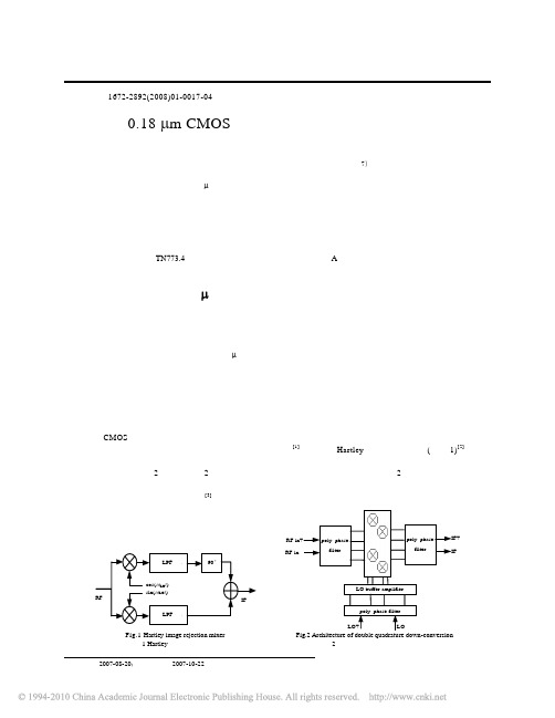
Fig.3 Schematic of RF poly-phase filter 图 3 RF 多相滤波器原理图
Fig.6 Gain of the buffer amplifier 图 6 缓冲放大器的增益
2 宽带镜像抑制混频器的设计
2.1 核心混频器单元的设计
在有源 Gilbert 双平衡的设计中,最常用的就是 Gilbert 双平衡结构[6-7]。该设计中的混频器结构如图 7。 该结构具有较低的本振功率、较高的变频增益、高的 LO-IF 和 RF-IF 的端口隔离度的优点。混频器中,变 频电压增益为[8-9]:
(2)
式中: un 为电子迁移率; Cox 为单位面积的栅氧化层电容;W/L为宽长比; Vgs 为栅源间电压; Vth 为管子的阈值
电压; Id 为偏置电流。 采用 TSMC 0.18 µm CMOS 管工艺,在 ADS2003 中利用谐波仿真得到的结果如表 2。
RL
RL
VCC
M3 M4 Vbias_LOp
performance
Gilbert cell
this work
gain/dB noise figure/dB Image rejection/dB
P-1/dBm RF-IF isolation/dB IF-LO isolation/dB LO-RF isolation/dB
broadcast-probe reply disable

broadcast-probe reply disablebroadcast-probe reply disable是一种网络设置的功能,它可以禁用网络广播探测的回复。
广播探测是广播一条消息,然后等待网络上所有的设备回复,以确定网络上的设备数量和类型。
这可以帮助管理员识别网络中的设备并进行故障排查。
然而,在某些情况下,禁用广播探测的回复可能是有用的。
一种常见的情况是在网络中存在大量的设备,这样会导致广播探测的回复产生大量的网络流量。
在某些情况下,网络流量可能会造成网络拥塞,并影响正常的网络通信。
此时,禁用广播探测的回复可以有效减少网络流量,提高网络的性能和稳定性。
另一种情况是在网络中存在安全隐患的情况下,禁用广播探测的回复可以增加网络的安全性。
广播探测的回复可以泄露网络上存在的设备,包括类型、版本等信息,这可能会被黑客用来进行网络攻击和入侵。
通过禁用广播探测的回复,可以减少黑客获取有关网络设备的信息的机会,从而提高网络的安全性。
为了禁用广播探测的回复,可以按照以下步骤进行操作:1. 登录到网络设备的管理界面。
这通常需要管理员账户和密码。
2. 寻找关于广播探测的配置选项。
这在不同的设备上可能有所不同,可以参考设备的用户手册或询问设备制造商的技术支持。
3. 在广播探测的配置选项中,找到相关的设置项。
可能会有一个名为"broadcast-probe reply"的选项。
4. 将该选项的值设置为"disable"。
有些设备可能使用其他关键字或选项来实现相同的功能,可以根据设备的文档或技术支持找到正确的设置。
5. 保存更改并重新启动网络设备。
在重新启动后,网络设备将禁止回复广播探测。
需要注意的是,禁用广播探测的回复可能会影响一些网络的功能和管理任务。
例如,一些网络管理工具可能依赖广播探测来识别设备并进行管理操作。
在禁用广播探测的回复之前,应该对网络进行细致的分析和评估,以确保禁用这个功能不会对网络的正常运行造成不利影响。
GSM900DCS1800系统 ”题库
“GSM900/DCS1800系统”题库一. 选择题1、切换由____C____ 启动。
A MSB BTSC BSCD MSC2、以下____D____ 存储于HLR中。
A TMSIB 鉴权三人组C LAID 用户业务信息3.以下___B_____不用鉴权。
A 位置更新B 切换流程C 手机主叫D 手机被叫4.DCS 1800系统的ARFCN总数为(C)。
A 124B 376C 374D 3755、*下列____B ___条件下,BSC无法控制BTS 。
A BTS_TEL FLTB BTS_O&M FLTC CLLK FOSD RA FOS6、SBL____B______与OMC_R和G2 BSC之间的X.25 link 有关。
A DTC 5B CPR 4C ATR 5D CPR 17、BSS的告警级别中,最严重的级别是 _C_。
A DMAB MIC VPMAD PMA8、 G3 BTS信令静态复用情况下一根Abis线最多连__C____个TRE。
A 8B 10C 12D 149、以下( C )不可执行跳频操作。
A. SDCCHB. SACCHC. BCCHD. TCH10. 参数INTFBD1…INTFBD5 把基站在空闲信道上收到的上行干扰情况分为5个等级, 其中反映干扰最严重的是(D)A Interference Band 1B Interference Band 2C Interference Band 4D Interference Band 511.ALCATEL BTS设备接地电阻要求小于(B)A.3欧姆 B.5欧姆C.10欧姆 D.15欧姆12.ALCATEL BTS设备2M传输线距离一般为(B)A.20MB.25MC.30MD.50M13.在天线安装过程中,我们要求二个扇区天线夹角应(B)A.小于90°B.大于90°C.等于120°D.都可以14.在馈线布放过程中,应注意(C)A.7/8馈线不能大于75米 B.接地不能少于3点C.馈线不能有扭曲或破损 D.馈线只能采用7/8”15.G3 BTS电压适应范围是(D)A.-48~-60VB.-48~-72VC.-39~-54VD.-39~-72V16.小区选择C1算法跟以下那个因素有关?( C )A)Rxlev_minB)MS_Txpwr_MaxC)Rxlev_Access_MinD)BS_Txpwr_Max17.由于阻挡物而产生的类似阴影效果的无线信号衰落称为:CA)多径衰落B)快衰落C)慢衰落D)路径衰落18.如果一个网络运营商分别有15 MHz的上、下行频宽,那么他可以获得多少个GSM 频点 (减去一个保护频点)? DA)600B)599C)75D)7419. 1W=____C__dBmA)10B)20C)30D)3320.为避免因过多跨越LAC的小区重选而造成的SDCCH的阻塞,我们将与该小区有切换关系且与之LAC不同的相邻小区的( B )参数提高?A)T3212B)Cell_Reselect_HysteresisC)Cell_Reselect_offsetD)Rxlev_Access_Min21. CONFIG 4的G2 BSC 需接__B___块GS-1。
NuMicro N9H30系列开发板用户手册说明书
NuMicro®FamilyArm® ARM926EJ-S BasedNuMaker-HMI-N9H30User ManualEvaluation Board for NuMicro® N9H30 SeriesNUMAKER-HMI-N9H30 USER MANUALThe information described in this document is the exclusive intellectual property ofNuvoton Technology Corporation and shall not be reproduced without permission from Nuvoton.Nuvoton is providing this document only for reference purposes of NuMicro microcontroller andmicroprocessor based system design. Nuvoton assumes no responsibility for errors or omissions.All data and specifications are subject to change without notice.For additional information or questions, please contact: Nuvoton Technology Corporation.Table of Contents1OVERVIEW (5)1.1Features (7)1.1.1NuMaker-N9H30 Main Board Features (7)1.1.2NuDesign-TFT-LCD7 Extension Board Features (7)1.2Supporting Resources (8)2NUMAKER-HMI-N9H30 HARDWARE CONFIGURATION (9)2.1NuMaker-N9H30 Board - Front View (9)2.2NuMaker-N9H30 Board - Rear View (14)2.3NuDesign-TFT-LCD7 - Front View (20)2.4NuDesign-TFT-LCD7 - Rear View (21)2.5NuMaker-N9H30 and NuDesign-TFT-LCD7 PCB Placement (22)3NUMAKER-N9H30 AND NUDESIGN-TFT-LCD7 SCHEMATICS (24)3.1NuMaker-N9H30 - GPIO List Circuit (24)3.2NuMaker-N9H30 - System Block Circuit (25)3.3NuMaker-N9H30 - Power Circuit (26)3.4NuMaker-N9H30 - N9H30F61IEC Circuit (27)3.5NuMaker-N9H30 - Setting, ICE, RS-232_0, Key Circuit (28)NUMAKER-HMI-N9H30 USER MANUAL3.6NuMaker-N9H30 - Memory Circuit (29)3.7NuMaker-N9H30 - I2S, I2C_0, RS-485_6 Circuit (30)3.8NuMaker-N9H30 - RS-232_2 Circuit (31)3.9NuMaker-N9H30 - LCD Circuit (32)3.10NuMaker-N9H30 - CMOS Sensor, I2C_1, CAN_0 Circuit (33)3.11NuMaker-N9H30 - RMII_0_PF Circuit (34)3.12NuMaker-N9H30 - RMII_1_PE Circuit (35)3.13NuMaker-N9H30 - USB Circuit (36)3.14NuDesign-TFT-LCD7 - TFT-LCD7 Circuit (37)4REVISION HISTORY (38)List of FiguresFigure 1-1 Front View of NuMaker-HMI-N9H30 Evaluation Board (5)Figure 1-2 Rear View of NuMaker-HMI-N9H30 Evaluation Board (6)Figure 2-1 Front View of NuMaker-N9H30 Board (9)Figure 2-2 Rear View of NuMaker-N9H30 Board (14)Figure 2-3 Front View of NuDesign-TFT-LCD7 Board (20)Figure 2-4 Rear View of NuDesign-TFT-LCD7 Board (21)Figure 2-5 Front View of NuMaker-N9H30 PCB Placement (22)Figure 2-6 Rear View of NuMaker-N9H30 PCB Placement (22)Figure 2-7 Front View of NuDesign-TFT-LCD7 PCB Placement (23)Figure 2-8 Rear View of NuDesign-TFT-LCD7 PCB Placement (23)Figure 3-1 GPIO List Circuit (24)Figure 3-2 System Block Circuit (25)Figure 3-3 Power Circuit (26)Figure 3-4 N9H30F61IEC Circuit (27)Figure 3-5 Setting, ICE, RS-232_0, Key Circuit (28)Figure 3-6 Memory Circuit (29)Figure 3-7 I2S, I2C_0, RS-486_6 Circuit (30)Figure 3-8 RS-232_2 Circuit (31)Figure 3-9 LCD Circuit (32)NUMAKER-HMI-N9H30 USER MANUAL Figure 3-10 CMOS Sensor, I2C_1, CAN_0 Circuit (33)Figure 3-11 RMII_0_PF Circuit (34)Figure 3-12 RMII_1_PE Circuit (35)Figure 3-13 USB Circuit (36)Figure 3-14 TFT-LCD7 Circuit (37)List of TablesTable 2-1 LCD Panel Combination Connector (CON8) Pin Function (11)Table 2-2 Three Sets of Indication LED Functions (12)Table 2-3 Six Sets of User SW, Key Matrix Functions (12)Table 2-4 CMOS Sensor Connector (CON10) Function (13)Table 2-5 JTAG ICE Interface (J2) Function (14)Table 2-6 Expand Port (CON7) Function (16)Table 2-7 UART0 (J3) Function (16)Table 2-8 UART2 (J6) Function (16)Table 2-9 RS-485_6 (SW6~8) Function (17)Table 2-10 Power on Setting (SW4) Function (17)Table 2-11 Power on Setting (S2) Function (17)Table 2-12 Power on Setting (S3) Function (17)Table 2-13 Power on Setting (S4) Function (17)Table 2-14 Power on Setting (S5) Function (17)Table 2-15 Power on Setting (S7/S6) Function (18)Table 2-16 Power on Setting (S9/S8) Function (18)Table 2-17 CMOS Sensor Connector (CON9) Function (19)Table 2-18 CAN_0 (SW9~10) Function (19)NUMAKER-HMI-N9H30 USER MANUAL1 OVERVIEWThe NuMaker-HMI-N9H30 is an evaluation board for GUI application development. The NuMaker-HMI-N9H30 consists of two parts: a NuMaker-N9H30 main board and a NuDesign-TFT-LCD7 extensionboard. The NuMaker-HMI-N9H30 is designed for project evaluation, prototype development andvalidation with HMI (Human Machine Interface) function.The NuMaker-HMI-N9H30 integrates touchscreen display, voice input/output, rich serial port serviceand I/O interface, providing multiple external storage methods.The NuDesign-TFT-LCD7 can be plugged into the main board via the DIN_32x2 extension connector.The NuDesign-TFT-LCD7 includes one 7” LCD which the resolution is 800x480 with RGB-24bits andembedded the 4-wires resistive type touch panel.Figure 1-1 Front View of NuMaker-HMI-N9H30 Evaluation BoardNUMAKER-HMI-N9H30 USER MANUAL Figure 1-2 Rear View of NuMaker-HMI-N9H30 Evaluation Board1.1 Features1.1.1 NuMaker-N9H30 Main Board Features●N9H30F61IEC chip: LQFP216 pin MCP package with DDR (64 MB)●SPI Flash using W25Q256JVEQ (32 MB) booting with quad mode or storage memory●NAND Flash using W29N01HVSINA (128 MB) booting or storage memory●One Micro-SD/TF card slot served either as a SD memory card for data storage or SDIO(Wi-Fi) device●Two sets of COM ports:–One DB9 RS-232 port with UART_0 used 75C3232E transceiver chip can be servedfor function debug and system development.–One DB9 RS-232 port with UART_2 used 75C3232E transceiver chip for userapplication●22 GPIO expansion ports, including seven sets of UART functions●JTAG interface provided for software development●Microphone input and Earphone/Speaker output with 24-bit stereo audio codec(NAU88C22) for I2S interfaces●Six sets of user-configurable push button keys●Three sets of LEDs for status indication●Provides SN65HVD230 transceiver chip for CAN bus communication●Provides MAX3485 transceiver chip for RS-485 device connection●One buzzer device for program applicationNUMAKER-HMI-N9H30 USER MANUAL●Two sets of RJ45 ports with Ethernet 10/100 Mbps MAC used IP101GR PHY chip●USB_0 that can be used as Device/HOST and USB_1 that can be used as HOSTsupports pen drives, keyboards, mouse and printers●Provides over-voltage and over current protection used APL3211A chip●Retain RTC battery socket for CR2032 type and ADC0 detect battery voltage●System power could be supplied by DC-5V adaptor or USB VBUS1.1.2 NuDesign-TFT-LCD7 Extension Board Features●7” resolution 800x480 4-wire resistive touch panel for 24-bits RGB888 interface●DIN_32x2 extension connector1.2 Supporting ResourcesFor sample codes and introduction about NuMaker-N9H30, please refer to N9H30 BSP:https:///products/gui-solution/gui-platform/numaker-hmi-n9h30/?group=Software&tab=2Visit NuForum for further discussion about the NuMaker-HMI-N9H30:/viewforum.php?f=31 NUMAKER-HMI-N9H30 USER MANUALNUMAKER-HMI-N9H30 USER MANUAL2 NUMAKER-HMI-N9H30 HARDWARE CONFIGURATION2.1 NuMaker-N9H30 Board - Front View Combination Connector (CON8)6 set User SWs (K1~6)3set Indication LEDs (LED1~3)Power Supply Switch (SW_POWER1)Audio Codec(U10)Microphone(M1)NAND Flash(U9)RS-232 Transceiver(U6, U12)RS-485 Transceiver(U11)CAN Transceiver (U13)Figure 2-1 Front View of NuMaker-N9H30 BoardFigure 2-1 shows the main components and connectors from the front side of NuMaker-N9H30 board. The following lists components and connectors from the front view:NuMaker-N9H30 board and NuDesign-TFT-LCD7 board combination connector (CON8). This panel connector supports 4-/5-wire resistive touch or capacitance touch panel for 24-bits RGB888 interface.Connector GPIO pin of N9H30 FunctionCON8.1 - Power 3.3VCON8.2 - Power 3.3VCON8.3 GPD7 LCD_CSCON8.4 GPH3 LCD_BLENCON8.5 GPG9 LCD_DENCON8.7 GPG7 LCD_HSYNCCON8.8 GPG6 LCD_CLKCON8.9 GPD15 LCD_D23(R7)CON8.10 GPD14 LCD_D22(R6)CON8.11 GPD13 LCD_D21(R5)CON8.12 GPD12 LCD_D20(R4)CON8.13 GPD11 LCD_D19(R3)CON8.14 GPD10 LCD_D18(R2)CON8.15 GPD9 LCD_D17(R1)CON8.16 GPD8 LCD_D16(R0)CON8.17 GPA15 LCD_D15(G7)CON8.18 GPA14 LCD_D14(G6)CON8.19 GPA13 LCD_D13(G5)CON8.20 GPA12 LCD_D12(G4)CON8.21 GPA11 LCD_D11(G3)CON8.22 GPA10 LCD_D10(G2)CON8.23 GPA9 LCD_D9(G1) NUMAKER-HMI-N9H30 USER MANUALCON8.24 GPA8 LCD_D8(G0)CON8.25 GPA7 LCD_D7(B7)CON8.26 GPA6 LCD_D6(B6)CON8.27 GPA5 LCD_D5(B5)CON8.28 GPA4 LCD_D4(B4)CON8.29 GPA3 LCD_D3(B3)CON8.30 GPA2 LCD_D2(B2)CON8.31 GPA1 LCD_D1(B1)CON8.32 GPA0 LCD_D0(B0)CON8.33 - -CON8.34 - -CON8.35 - -CON8.36 - -CON8.37 GPB2 LCD_PWMCON8.39 - VSSCON8.40 - VSSCON8.41 ADC7 XPCON8.42 ADC3 VsenCON8.43 ADC6 XMCON8.44 ADC4 YMCON8.45 - -CON8.46 ADC5 YPCON8.47 - VSSCON8.48 - VSSCON8.49 GPG0 I2C0_CCON8.50 GPG1 I2C0_DCON8.51 GPG5 TOUCH_INTCON8.52 - -CON8.53 - -CON8.54 - -CON8.55 - -NUMAKER-HMI-N9H30 USER MANUAL CON8.56 - -CON8.57 - -CON8.58 - -CON8.59 - VSSCON8.60 - VSSCON8.61 - -CON8.62 - -CON8.63 - Power 5VCON8.64 - Power 5VTable 2-1 LCD Panel Combination Connector (CON8) Pin Function●Power supply switch (SW_POWER1): System will be powered on if the SW_POWER1button is pressed●Three sets of indication LEDs:LED Color DescriptionsLED1 Red The system power will beterminated and LED1 lightingwhen the input voltage exceeds5.7V or the current exceeds 2A.LED2 Green Power normal state.LED3 Green Controlled by GPH2 pin Table 2-2 Three Sets of Indication LED Functions●Six sets of user SW, Key Matrix for user definitionKey GPIO pin of N9H30 FunctionK1 GPF10 Row0 GPB4 Col0K2 GPF10 Row0 GPB5 Col1K3 GPE15 Row1 GPB4 Col0K4 GPE15 Row1 GPB5 Col1K5 GPE14 Row2 GPB4 Col0K6GPE14 Row2GPB5 Col1 Table 2-3 Six Sets of User SW, Key Matrix Functions●NAND Flash (128 MB) with Winbond W29N01HVS1NA (U9)●Microphone (M1): Through Nuvoton NAU88C22 chip sound input●Audio CODEC chip (U10): Nuvoton NAU88C22 chip connected to N9H30 using I2Sinterface–SW6/SW7/SW8: 1-2 short for RS-485_6 function and connected to 2P terminal (CON5and J5)–SW6/SW7/SW8: 2-3 short for I2S function and connected to NAU88C22 (U10).●CMOS Sensor connector (CON10, SW9~10)–SW9~10: 1-2 short for CAN_0 function and connected to 2P terminal (CON11)–SW9~10: 2-3 short for CMOS sensor function and connected to CMOS sensorconnector (CON10)Connector GPIO pin of N9H30 FunctionCON10.1 - VSSCON10.2 - VSSNUMAKER-HMI-N9H30 USER MANUALCON10.3 - Power 3.3VCON10.4 - Power 3.3VCON10.5 - -CON10.6 - -CON10.7 GPI4 S_PCLKCON10.8 GPI3 S_CLKCON10.9 GPI8 S_D0CON10.10 GPI9 S_D1CON10.11 GPI10 S_D2CON10.12 GPI11 S_D3CON10.13 GPI12 S_D4CON10.14 GPI13 S_D5CON10.15 GPI14 S_D6CON10.16 GPI15 S_D7CON10.17 GPI6 S_VSYNCCON10.18 GPI5 S_HSYNCCON10.19 GPI0 S_PWDNNUMAKER-HMI-N9H30 USER MANUAL CON10.20 GPI7 S_nRSTCON10.21 GPG2 I2C1_CCON10.22 GPG3 I2C1_DCON10.23 - VSSCON10.24 - VSSTable 2-4 CMOS Sensor Connector (CON10) FunctionNUMAKER-HMI-N9H30 USER MANUAL2.2NuMaker-N9H30 Board - Rear View5V In (CON1)RS-232 DB9 (CON2,CON6)Expand Port (CON7)Speaker Output (J4)Earphone Output (CON4)Buzzer (BZ1)System ResetSW (SW5)SPI Flash (U7,U8)JTAG ICE (J2)Power ProtectionIC (U1)N9H30F61IEC (U5)Micro SD Slot (CON3)RJ45 (CON12, CON13)USB1 HOST (CON15)USB0 Device/Host (CON14)CAN_0 Terminal (CON11)CMOS Sensor Connector (CON9)Power On Setting(SW4, S2~S9)RS-485_6 Terminal (CON5)RTC Battery(BT1)RMII PHY (U14,U16)Figure 2-2 Rear View of NuMaker-N9H30 BoardFigure 2-2 shows the main components and connectors from the rear side of NuMaker-N9H30 board. The following lists components and connectors from the rear view:● +5V In (CON1): Power adaptor 5V input ●JTAG ICE interface (J2) ConnectorGPIO pin of N9H30Function J2.1 - Power 3.3V J2.2 GPJ4 nTRST J2.3 GPJ2 TDI J2.4 GPJ1 TMS J2.5 GPJ0 TCK J2.6 - VSS J2.7 GPJ3 TD0 J2.8-RESETTable 2-5 JTAG ICE Interface (J2) Function●SPI Flash (32 MB) with Winbond W25Q256JVEQ (U7); only one (U7 or U8) SPI Flashcan be used●System Reset (SW5): System will be reset if the SW5 button is pressed●Buzzer (BZ1): Control by GPB3 pin of N9H30●Speaker output (J4): Through the NAU88C22 chip sound output●Earphone output (CON4): Through the NAU88C22 chip sound output●Expand port for user use (CON7):Connector GPIO pin of N9H30 FunctionCON7.1 - Power 3.3VCON7.2 - Power 3.3VCON7.3 GPE12 UART3_TXDCON7.4 GPH4 UART1_TXDCON7.5 GPE13 UART3_RXDCON7.6 GPH5 UART1_RXDCON7.7 GPB0 UART5_TXDCON7.8 GPH6 UART1_RTSCON7.9 GPB1 UART5_RXDCON7.10 GPH7 UART1_CTSCON7.11 GPI1 UART7_TXDNUMAKER-HMI-N9H30 USER MANUAL CON7.12 GPH8 UART4_TXDCON7.13 GPI2 UART7_RXDCON7.14 GPH9 UART4_RXDCON7.15 - -CON7.16 GPH10 UART4_RTSCON7.17 - -CON7.18 GPH11 UART4_CTSCON7.19 - VSSCON7.20 - VSSCON7.21 GPB12 UART10_TXDCON7.22 GPH12 UART8_TXDCON7.23 GPB13 UART10_RXDCON7.24 GPH13 UART8_RXDCON7.25 GPB14 UART10_RTSCON7.26 GPH14 UART8_RTSCON7.27 GPB15 UART10_CTSCON7.28 GPH15 UART8_CTSCON7.29 - Power 5VCON7.30 - Power 5VTable 2-6 Expand Port (CON7) Function●UART0 selection (CON2, J3):–RS-232_0 function and connected to DB9 female (CON2) for debug message output.–GPE0/GPE1 connected to 2P terminal (J3).Connector GPIO pin of N9H30 Function J3.1 GPE1 UART0_RXDJ3.2 GPE0 UART0_TXDTable 2-7 UART0 (J3) Function●UART2 selection (CON6, J6):–RS-232_2 function and connected to DB9 female (CON6) for debug message output –GPF11~14 connected to 4P terminal (J6)Connector GPIO pin of N9H30 Function J6.1 GPF11 UART2_TXDJ6.2 GPF12 UART2_RXDJ6.3 GPF13 UART2_RTSJ6.4 GPF14 UART2_CTSTable 2-8 UART2 (J6) Function●RS-485_6 selection (CON5, J5, SW6~8):–SW6~8: 1-2 short for RS-485_6 function and connected to 2P terminal (CON5 and J5) –SW6~8: 2-3 short for I2S function and connected to NAU88C22 (U10)Connector GPIO pin of N9H30 FunctionSW6:1-2 shortGPG11 RS-485_6_DISW6:2-3 short I2S_DOSW7:1-2 shortGPG12 RS-485_6_ROSW7:2-3 short I2S_DISW8:1-2 shortGPG13 RS-485_6_ENBSW8:2-3 short I2S_BCLKNUMAKER-HMI-N9H30 USER MANUALTable 2-9 RS-485_6 (SW6~8) FunctionPower on setting (SW4, S2~9).SW State FunctionSW4.2/SW4.1 ON/ON Boot from USB SW4.2/SW4.1 ON/OFF Boot from eMMC SW4.2/SW4.1 OFF/ON Boot from NAND Flash SW4.2/SW4.1 OFF/OFF Boot from SPI Flash Table 2-10 Power on Setting (SW4) FunctionSW State FunctionS2 Short System clock from 12MHzcrystalS2 Open System clock from UPLL output Table 2-11 Power on Setting (S2) FunctionSW State FunctionS3 Short Watchdog Timer OFFS3 Open Watchdog Timer ON Table 2-12 Power on Setting (S3) FunctionSW State FunctionS4 Short GPJ[4:0] used as GPIO pinS4Open GPJ[4:0] used as JTAG ICEinterfaceTable 2-13 Power on Setting (S4) FunctionSW State FunctionS5 Short UART0 debug message ONS5 Open UART0 debug message OFFTable 2-14 Power on Setting (S5) FunctionSW State FunctionS7/S6 Short/Short NAND Flash page size 2KBS7/S6 Short/Open NAND Flash page size 4KBS7/S6 Open/Short NAND Flash page size 8KBNUMAKER-HMI-N9H30 USER MANUALS7/S6 Open/Open IgnoreTable 2-15 Power on Setting (S7/S6) FunctionSW State FunctionS9/S8 Short/Short NAND Flash ECC type BCH T12S9/S8 Short/Open NAND Flash ECC type BCH T15S9/S8 Open/Short NAND Flash ECC type BCH T24S9/S8 Open/Open IgnoreTable 2-16 Power on Setting (S9/S8) FunctionCMOS Sensor connector (CON9, SW9~10)–SW9~10: 1-2 short for CAN_0 function and connected to 2P terminal (CON11).–SW9~10: 2-3 short for CMOS sensor function and connected to CMOS sensorconnector (CON9).Connector GPIO pin of N9H30 FunctionCON9.1 - VSSCON9.2 - VSSCON9.3 - Power 3.3VCON9.4 - Power 3.3V NUMAKER-HMI-N9H30 USER MANUALCON9.5 - -CON9.6 - -CON9.7 GPI4 S_PCLKCON9.8 GPI3 S_CLKCON9.9 GPI8 S_D0CON9.10 GPI9 S_D1CON9.11 GPI10 S_D2CON9.12 GPI11 S_D3CON9.13 GPI12 S_D4CON9.14 GPI13 S_D5CON9.15 GPI14 S_D6CON9.16 GPI15 S_D7CON9.17 GPI6 S_VSYNCCON9.18 GPI5 S_HSYNCCON9.19 GPI0 S_PWDNCON9.20 GPI7 S_nRSTCON9.21 GPG2 I2C1_CCON9.22 GPG3 I2C1_DCON9.23 - VSSCON9.24 - VSSTable 2-17 CMOS Sensor Connector (CON9) Function●CAN_0 Selection (CON11, SW9~10):–SW9~10: 1-2 short for CAN_0 function and connected to 2P terminal (CON11) –SW9~10: 2-3 short for CMOS sensor function and connected to CMOS sensor connector (CON9, CON10)SW GPIO pin of N9H30 FunctionSW9:1-2 shortGPI3 CAN_0_RXDSW9:2-3 short S_CLKSW10:1-2 shortGPI4 CAN_0_TXDSW10:2-3 short S_PCLKTable 2-18 CAN_0 (SW9~10) Function●USB0 Device/HOST Micro-AB connector (CON14), where CON14 pin4 ID=1 is Device,ID=0 is HOST●USB1 for USB HOST with Type-A connector (CON15)●RJ45_0 connector with LED indicator (CON12), RMII PHY with IP101GR (U14)●RJ45_1 connector with LED indicator (CON13), RMII PHY with IP101GR (U16)●Micro-SD/TF card slot (CON3)●SOC CPU: Nuvoton N9H30F61IEC (U5)●Battery power for RTC 3.3V powered (BT1, J1), can detect voltage by ADC0●RTC power has 3 sources:–Share with 3.3V I/O power–Battery socket for CR2032 (BT1)–External connector (J1)●Board version 2.1NUMAKER-HMI-N9H30 USER MANUAL2.3 NuDesign-TFT-LCD7 -Front ViewFigure 2-3 Front View of NuDesign-TFT-LCD7 BoardFigure 2-3 shows the main components and connectors from the Front side of NuDesign-TFT-LCD7board.7” resolution 800x480 4-W resistive touch panel for 24-bits RGB888 interface2.4 NuDesign-TFT-LCD7 -Rear ViewFigure 2-4 Rear View of NuDesign-TFT-LCD7 BoardFigure 2-4 shows the main components and connectors from the rear side of NuDesign-TFT-LCD7board.NuMaker-N9H30 and NuDesign-TFT-LCD7 combination connector (CON1).NUMAKER-HMI-N9H30 USER MANUAL 2.5 NuMaker-N9H30 and NuDesign-TFT-LCD7 PCB PlacementFigure 2-5 Front View of NuMaker-N9H30 PCB PlacementFigure 2-6 Rear View of NuMaker-N9H30 PCB PlacementNUMAKER-HMI-N9H30 USER MANUALFigure 2-7 Front View of NuDesign-TFT-LCD7 PCB PlacementFigure 2-8 Rear View of NuDesign-TFT-LCD7 PCB Placement3 NUMAKER-N9H30 AND NUDESIGN-TFT-LCD7 SCHEMATICS3.1 NuMaker-N9H30 - GPIO List CircuitFigure 3-1 shows the N9H30F61IEC GPIO list circuit.Figure 3-1 GPIO List Circuit NUMAKER-HMI-N9H30 USER MANUAL3.2 NuMaker-N9H30 - System Block CircuitFigure 3-2 shows the System Block Circuit.NUMAKER-HMI-N9H30 USER MANUALFigure 3-2 System Block Circuit3.3 NuMaker-N9H30 - Power CircuitFigure 3-3 shows the Power Circuit.NUMAKER-HMI-N9H30 USER MANUALFigure 3-3 Power Circuit3.4 NuMaker-N9H30 - N9H30F61IEC CircuitFigure 3-4 shows the N9H30F61IEC Circuit.Figure 3-4 N9H30F61IEC CircuitNUMAKER-HMI-N9H30 USER MANUAL3.5 NuMaker-N9H30 - Setting, ICE, RS-232_0, Key CircuitFigure 3-5 shows the Setting, ICE, RS-232_0, Key Circuit.NUMAKER-HMI-N9H30 USER MANUALFigure 3-5 Setting, ICE, RS-232_0, Key Circuit3.6 NuMaker-N9H30 - Memory CircuitFigure 3-6 shows the Memory Circuit.NUMAKER-HMI-N9H30 USER MANUALFigure 3-6 Memory Circuit3.7 NuMaker-N9H30 - I2S, I2C_0, RS-485_6 CircuitFigure 3-7 shows the I2S, I2C_0, RS-486_6 Circuit.NUMAKER-HMI-N9H30 USER MANUALFigure 3-7 I2S, I2C_0, RS-486_6 Circuit3.8 NuMaker-N9H30 - RS-232_2 CircuitFigure 3-8 shows the RS-232_2 Circuit.NUMAKER-HMI-N9H30 USER MANUALFigure 3-8 RS-232_2 Circuit3.9 NuMaker-N9H30 - LCD CircuitFigure 3-9 shows the LCD Circuit.NUMAKER-HMI-N9H30 USER MANUALFigure 3-9 LCD Circuit3.10 NuMaker-N9H30 - CMOS Sensor, I2C_1, CAN_0 CircuitFigure 3-10 shows the CMOS Sensor,I2C_1, CAN_0 Circuit.NUMAKER-HMI-N9H30 USER MANUALFigure 3-10 CMOS Sensor, I2C_1, CAN_0 Circuit3.11 NuMaker-N9H30 - RMII_0_PF CircuitFigure 3-11 shows the RMII_0_RF Circuit.NUMAKER-HMI-N9H30 USER MANUALFigure 3-11 RMII_0_PF Circuit3.12 NuMaker-N9H30 - RMII_1_PE CircuitFigure 3-12 shows the RMII_1_PE Circuit.NUMAKER-HMI-N9H30 USER MANUALFigure 3-12 RMII_1_PE Circuit3.13 NuMaker-N9H30 - USB CircuitFigure 3-13 shows the USB Circuit.NUMAKER-HMI-N9H30 USER MANUALFigure 3-13 USB Circuit3.14 NuDesign-TFT-LCD7 - TFT-LCD7 CircuitFigure 3-14 shows the TFT-LCD7 Circuit.Figure 3-14 TFT-LCD7 CircuitNUMAKER-HMI-N9H30 USER MANUAL4 REVISION HISTORYDate Revision Description2022.03.24 1.00 Initial version NUMAKER-HMI-N9H30 USER MANUALNUMAKER-HMI-N9H30 USER MANUALImportant NoticeNuvoton Products are neither intended nor warranted for usage in systems or equipment, anymalfunction or failure of which may cause loss of human life, bodily injury or severe propertydamage. Such applications are deemed, “Insecure Usage”.Insecure usage includes, but is not limited to: equipment for surgical implementation, atomicenergy control instruments, airplane or spaceship instruments, the control or operation ofdynamic, brake or safety systems designed for vehicular use, traffic signal instruments, all typesof safety devices, and other applications intended to support or sustain life.All Insecure Usage shall be made at customer’s risk, and in the event that third parties lay claimsto Nuvoton as a result of customer’s Insecure Usage, custome r shall indemnify the damagesand liabilities thus incurred by Nuvoton.。
8200系列QAM调制器-用户手册课件
InfoLink DTX8200系列QAM调制器用户指南目录目录1 概述................................................................................................................................................ 1-11.1 简介............................................................................................................................................................... 1-21.2 特性............................................................................................................................................................... 1-31.3 工作原理....................................................................................................................................................... 1-42 设备描述........................................................................................................................................ 2-12.1 设备描述....................................................................................................................................................... 2-22.1.1 设备外观 ............................................................................................................................................. 2-22.1.2 前面板 ................................................................................................................................................. 2-22.1.3 功能键 ................................................................................................................................................. 2-22.1.4 后面板 ................................................................................................................................................. 2-32.2 接口描述....................................................................................................................................................... 2-42.3 设备操作菜单............................................................................................................................................... 2-53 安装指南........................................................................................................................................ 3-13.1 安装流程....................................................................................................................................................... 3-23.2 安装机箱....................................................................................................................................................... 3-23.3 连接线缆....................................................................................................................................................... 3-33.3.1 安装说明 ............................................................................................................................................. 3-33.3.2 连接地线 ............................................................................................................................................. 3-43.3.3 连接DS3输入和输出线缆................................................................................................................. 3-43.3.4 连接ASI输入和输出线缆 ................................................................................................................. 3-53.3.5 连接SPI输入线缆.............................................................................................................................. 3-63.3.6 连接IF中频输入/输出线缆 ............................................................................................................... 3-73.3.7 连接RF射频输出线缆....................................................................................................................... 3-83.3.8 连接10/100M网口 ............................................................................................................................. 3-93.3.9 连接电源线........................................................................................................................................ 3-103.4 启动设备..................................................................................................................................................... 3-114 配置设备参数................................................................................................................................ 4-14.1 配置概述....................................................................................................................................................... 4-24.2 选择输入接口............................................................................................................................................... 4-3目录InfoLink DTX8200系列QAM调制器用户指南4.3 设置DS3模式.............................................................................................................................................. 4-44.3.1 选择模式 ............................................................................................................................................. 4-44.3.2 设置主/备模式号 ................................................................................................................................ 4-54.3.3 搜索模式号.......................................................................................................................................... 4-6 4.4 输出设置....................................................................................................................................................... 4-64.4.1 设置输出频率...................................................................................................................................... 4-64.4.2 设置输出频道...................................................................................................................................... 4-74.4.3 设置QAM调制数 .............................................................................................................................. 4-84.4.4 设置符号率.......................................................................................................................................... 4-94.4.5 设置输出码率...................................................................................................................................... 4-94.4.6 设置射频控制.................................................................................................................................... 4-104.4.7 设置输出增益.................................................................................................................................... 4-114.4.8 设置频谱翻转.................................................................................................................................... 4-11 4.5 码流处理..................................................................................................................................................... 4-124.5.1 设置PID过滤 ................................................................................................................................... 4-124.5.2 设置PID映射 ................................................................................................................................... 4-134.5.3 设置PID插入 ................................................................................................................................... 4-155 配置网络参数................................................................................................................................ 5-15.1 组网简介....................................................................................................................................................... 5-25.2 设置网管IP地址 ......................................................................................................................................... 5-25.3 设置以太网口参数....................................................................................................................................... 5-35.3.1 设置IP地址 ........................................................................................................................................ 5-35.3.2 设置子网掩码...................................................................................................................................... 5-35.3.3 设置网关地址...................................................................................................................................... 5-45.3.4 设置网口模式...................................................................................................................................... 5-55.4 配置TS网口参数 ........................................................................................................................................ 5-55.4.1 打开网口 ............................................................................................................................................. 5-55.4.2 设置IP地址 ........................................................................................................................................ 5-65.4.3 设置子网掩码...................................................................................................................................... 5-65.4.4 设置网管PID ...................................................................................................................................... 5-75.5 配置透明传输网口参数............................................................................................................................... 5-75.5.1 透明传输示例...................................................................................................................................... 5-75.5.2 打开网口 ............................................................................................................................................. 5-85.5.3 设置IP地址 ........................................................................................................................................ 5-85.5.4 设置子网掩码...................................................................................................................................... 5-95.5.5 设置网关地址...................................................................................................................................... 5-95.5.6 设置网元IP ......................................................................................................................................... 5-95.5.7 设置源地址........................................................................................................................................ 5-105.5.8 设置目标地址.................................................................................................................................... 5-11InfoLink DTX8200系列QAM调制器用户指南目录6 典型业务配置................................................................................................................................ 6-16.1 配置复用....................................................................................................................................................... 6-26.2 配置调制....................................................................................................................................................... 6-57 升级指南........................................................................................................................................ 7-17.1 升级准备....................................................................................................................................................... 7-27.2 升级执行....................................................................................................................................................... 7-27.2.1 通过网管系统升级软件...................................................................................................................... 7-37.2.2 通过FTP服务器升级......................................................................................................................... 7-48 例行维护........................................................................................................................................ 8-18.1 设备例行维护项目....................................................................................................................................... 8-28.2 日维护项目................................................................................................................................................... 8-28.3 月维护项目................................................................................................................................................... 8-48.4 年维护项目................................................................................................................................................... 8-68.5 维护表........................................................................................................................................................... 8-78.5.1 日维护表 ............................................................................................................................................. 8-78.5.2 月维护表 ............................................................................................................................................. 8-88.5.3 年维护表 ............................................................................................................................................. 8-99 告警处理........................................................................................................................................ 9-19.1 告警信息处理............................................................................................................................................... 9-29.1.1 查看告警信息...................................................................................................................................... 9-29.1.2 保存告警信息...................................................................................................................................... 9-29.1.3 删除告警信息...................................................................................................................................... 9-29.2 常见告警及处理建议................................................................................................................................... 9-39.2.1 码流类告警.......................................................................................................................................... 9-39.2.2 升级类告警.......................................................................................................................................... 9-49.2.3 其它 ..................................................................................................................................................... 9-410 故障处理.................................................................................................................................... 10-110.1 输入输出故障处理................................................................................................................................... 10-210.1.1 射频信号无输出.............................................................................................................................. 10-210.1.2 射频信号输出偏低.......................................................................................................................... 10-210.1.3 设备输入码流中断.......................................................................................................................... 10-210.2 接收与显示节目故障处理....................................................................................................................... 10-310.2.1 STB不能正常解码节目.................................................................................................................. 10-310.2.2 混频后STB搜索不到节目............................................................................................................. 10-310.2.3 无电视信号...................................................................................................................................... 10-410.2.4 过滤后节目还存在.......................................................................................................................... 10-410.2.5 插入PSI/SI信息导致STB工作异常 ............................................................................................ 10-410.2.6 映射后的节目未能正常播放.......................................................................................................... 10-5目录InfoLink DTX8200系列QAM调制器用户指南10.2.7 图像显示马赛克或定帧.................................................................................................................. 10-5 10.3 网管管理设备故障处理........................................................................................................................... 10-610.3.1 网管不能提取PSI/SI信息 ............................................................................................................. 10-610.3.2 网管不能控制添加的设备.............................................................................................................. 10-610.3.3 网管软件未能成功提取PSI/SI表信息.......................................................................................... 10-711 FAQ ........................................................................................................................................... 11-111.1 名词解释FAQ .......................................................................................................................................... 11-211.2 操作应用FAQ .......................................................................................................................................... 11-3InfoLink DTX8200系列QAM调制器用户指南插图目录插图目录图1-1 DTX8200在数字电视前端的应用......................................................................................................... 1-2图1-2 DTX8200总体结构示意图..................................................................................................................... 1-4图2-1 DTX8200外观示意图............................................................................................................................. 2-2图2-2 DTX8200前面板示意图......................................................................................................................... 2-2图2-3 DTX8208后面板 .................................................................................................................................... 2-3图2-4 DTX8209后面板 .................................................................................................................................... 2-3图2-5 DTX8210后面板 .................................................................................................................................... 2-3图2-6 DTX8211与DTX8211E后面板............................................................................................................. 2-4图2-7 DTX8200接口图 .................................................................................................................................... 2-4图2-8 信息查询项 ............................................................................................................................................. 2-6图2-9 码流处理项 ............................................................................................................................................. 2-6图2-10 输出设置项 ........................................................................................................................................... 2-6图2-11 输入设置项............................................................................................................................................ 2-7图2-12 网络设置 ............................................................................................................................................... 2-7图2-13 系统设置 ............................................................................................................................................... 2-8图3-1 DTX8200安装流程................................................................................................................................. 3-2图3-2 DTX8200的固定 .................................................................................................................................... 3-2图3-3 连接地线 ................................................................................................................................................. 3-4图3-4 75Ω同轴线缆.......................................................................................................................................... 3-4图3-5 DS3输入、输出连接示意图.................................................................................................................. 3-5图3-6 ASI输入、输出连接示意图................................................................................................................... 3-6图3-7 SPI线缆................................................................................................................................................... 3-7图3-8 SPI线缆连接示意图............................................................................................................................... 3-7图3-9 IF输入、IF输出自环连接示意图......................................................................................................... 3-8图3-10 RF射频输出连接示意图...................................................................................................................... 3-9插图目录InfoLink DTX8200系列QAM调制器用户指南图3-11 10/100M网线 ........................................................................................................................................ 3-9图3-12 连接10/100M网口示意图 ................................................................................................................. 3-10图3-13 连接电源和地线.................................................................................................................................. 3-10图3-14 DTX8200启动显示............................................................................................................................. 3-11图4-1 设置过滤参数 ....................................................................................................................................... 4-13图4-2 设置映射参数 ....................................................................................................................................... 4-15图5-1 设置网口IP地址 .................................................................................................................................... 5-3图5-2 设置网口子网掩码.................................................................................................................................. 5-4图5-3 设置网关地址 ......................................................................................................................................... 5-4图5-4 设置网口模式 ......................................................................................................................................... 5-5图5-5 打开TS网口........................................................................................................................................... 5-6图5-6 设置TS网口IP地址.............................................................................................................................. 5-6图5-7 设置TS网口子网掩码 ........................................................................................................................... 5-6图5-8 设置网管PID .......................................................................................................................................... 5-7图5-9 透明传输示例 ......................................................................................................................................... 5-8图5-10 打开透明传输网口................................................................................................................................ 5-8图5-11 设置透明传输网口IP地址 .................................................................................................................. 5-9图5-12 设置透明传输网口子网掩码................................................................................................................ 5-9图5-13 设置透明传输网口网关地址................................................................................................................ 5-9图5-14 设置透明传输网元IP ......................................................................................................................... 5-10图5-15 设置透明传输网口源地址.................................................................................................................. 5-10图5-16 设置透明传输网口目标地址.............................................................................................................. 5-11图6-1 配置组网图 ............................................................................................................................................. 6-2图6-2 基本配置 ................................................................................................................................................. 6-3图6-3 提取表信息 ............................................................................................................................................. 6-4图6-4 复用接口配置 ......................................................................................................................................... 6-5图6-5 配置组网图 ............................................................................................................................................. 6-6图7-1 启动FTP服务器软件............................................................................................................................. 7-2图7-2 升级软件界面 ......................................................................................................................................... 7-3图7-3 选择升级软件 ......................................................................................................................................... 7-4图7-4 设置升级服务器IP地址 ........................................................................................................................ 7-4图7-5 启动程序升级 ......................................................................................................................................... 7-5InfoLink DTX8200系列QAM调制器用户指南表格目录表格目录表2-1 功能及方向键说明.................................................................................................................................. 2-2表2-2 设备接口描述 ......................................................................................................................................... 2-5表3-1 DTX8200安装可选项............................................................................................................................. 3-3表4-1 配置顺序 ................................................................................................................................................. 4-2表4-2 输入接口可选项...................................................................................................................................... 4-3表4-3 模式参数选择 ......................................................................................................................................... 4-5表4-4 DS3模式号.............................................................................................................................................. 4-6表4-5 可选项参数 ............................................................................................................................................. 4-7表4-6 输出频率规划 ......................................................................................................................................... 4-7表4-7 输出频道参数选项.................................................................................................................................. 4-8表4-8 QAM调制数参数选项 ........................................................................................................................... 4-8表4-9 符号率参数选项...................................................................................................................................... 4-9表4-10 输出码率参数选项.............................................................................................................................. 4-10表4-11 射频信号选项...................................................................................................................................... 4-10表4-12 输出增益选项 ..................................................................................................................................... 4-11表4-13 频谱翻转选项 ..................................................................................................................................... 4-12表4-14 PID过滤选项 ...................................................................................................................................... 4-12表4-15 PID映射选项 ...................................................................................................................................... 4-14表4-16 PID插入选项 ...................................................................................................................................... 4-16表5-1 网管组网方式 ......................................................................................................................................... 5-2表6-1 基本流PID .............................................................................................................................................. 6-2表8-1 设备例行维护周期和维护项目.............................................................................................................. 8-2表8-2 设备的日维护项目.................................................................................................................................. 8-3表8-3 指示灯状态及说明.................................................................................................................................. 8-4表8-4 设备的月维护项目.................................................................................................................................. 8-5。
5G无线维护考试题及答案-华为设备

5G无线试题一、判断题1.FANc和FANd风扇板可以放置在BBU5900机框中使用。
()2.BBU5900的槽位编号是从左往右编排,再从上到下编排。
()3.操作时必须确保正确的ESD防护措施,如佩戴防静电腕带或手套,以避免单板、模块或电子部件遭到静电损害。
( )4.5GAAU模块使用双电源线供电方案时需要外接ODM,输入2路电源线输出转成1路电源线。
( )5、BBU3900与BBU5900槽位分布一致。
()6.IMB05机框挂墙是只允许竖放,不允许横放。
( )7.当前NSA场景主流的组网方案是Option 3x方案。
( )8.5G标准站点解决方案中AAU拉远距离需小于100米,超出100米的场景需单独申请特殊场景方案。
( )9.5G AAU支持级联。
()10.AAU本身有保护接地,在安装好保护接地线的情况下,AAU的电源线不需要剥开露出电源线屏蔽层进行固定。
( )11.pRRU支持级联。
()12.安装AAU电源线应注意:必须先连接AAU端连接器,再连接供电设备端连接器。
如果连接顺序错误或电源线极性反接,可能导致AAU设备损坏或人身伤害。
()13.目前已经发布的5G试点频段低频主要有2.6G、3.5G、4.9G、10G。
( )14.UMPTe3单板支持GPS及北斗。
()15.UPEUd电源板不能放置在BBU5900机框中使用。
( )一、单选题1、5G基站主控板推荐优先部署在BBU5900几号槽位(D )A.0B.3C.6D.72、DCDU-12B 电源模块的输出规格为(A)A.10路30AB.10路20AC.7路30AD.7路20A3、5G AAU使用的eCPRI光模块带宽大小是多少(B)A.10GEB.25GEC.50GED.100GE4、按照标准5G站点解决方案,BBU5900部署大于等于2个UBBPfw1全宽基带板时,需要配置UPEUe电源模块的数量为(B )A.1个B.2个C.1个或者2个均可以D、以上均不对5、按照标准站点解决方案,无功分器、放大器场景GPS最大拉远距离为(C )A.50mB.70mC.150mD.170m6、BBU5900安装在第三方机柜时为防止系统风量不足,建议相邻BBU之间预留(A )U或以上间距,并安装挡风板,避免风道回流A.1UB.3UC.5UD.6U7、5G BBU5900与传输对接使用的光模块带宽大小是多少CA.100MB.1GEC.10GED.100GE8、BBU5900 UPEUe电源模块输入电源线需要几路(直流电源线正负算1路)BA.1路B.2路C.3路D.5路9、5G 全宽基带板推荐部署在BBU5900的槽位优先级顺序为AA.0>2>4B.4>2>0C.4>2>0>1>3>5D.5>3>110、UPEUe的输出功率是(D)A、350WB、650WC、1100WD、2000W11、5G频谱规划中属于C-Band的频率是(C)A、800MHZB、2.6GHZ C 4.9GHZ D、35GHZ12、在5G编码之争中,华为主导的(B)最终成为5G控制信道编码标准。
低功耗接收芯片MAX1471

General DescriptionThe MAX1471 low-power, CMOS, superheterodyne, RF dual-channel receiver is designed to receive both ampli-tude-shift-keyed (ASK) and frequency-shift-keyed (FSK)data without reconfiguring the device or introducing any time delay normally associated with changing modula-tion schemes. The MAX1471 requires few external com-ponents to realize a complete wireless RF digital data receiver for the 300MHz to 450MHz ISM bands.The MAX1471 includes all the active components required in a superheterodyne receiver including: a low-noise amplifier (LNA), an image-reject (IR) mixer, a fully integrated phase-locked loop (PLL), local oscillator (LO), 10.7MHz IF limiting amplifier with received-signal-strength indicator (RSSI), low-noise F M demodulator,and a 3V voltage regulator. Differential peak-detecting data demodulators are included for both the F SK and ASK analog baseband data recovery. The MAX1471includes a discontinuous receive (DRX) mode for low-power operation, which is configured through a serial interface bus.The MAX1471 is available in a 32-pin thin QFN package and is specified over the automotive -40°C to +125°C temperature range.ApplicationsAutomotive Remote Keyless Entry (RKE)Tire Pressure Monitoring Systems Garage Door Openers Wireless Sensors Wireless Keys Security Systems Medical Systems Home Automation Local Telemetry SystemsFeatureso ASK and FSK Demodulated Data on Separate Outputso Specified over Automotive -40°C to +125°C Temperature Rangeo Low Operating Supply Voltage Down to 2.4V o On-Chip 3V Regulator for 5V Operation o Low Operating Supply Current7mA Continuous Receive Mode 1.1µA Deep-Sleep Modeo Discontinuous Receive (DRX) Low-Power Managemento Fast-On Startup Feature < 250µso Integrated PLL, VCO, and Loop Filter o 45dB Integrated Image Rejection o RF Input Sensitivity*ASK: -114dBm FSK: -108dBmo Selectable IF BW with External Filtero Programmable Through Serial User Interface o RSSI Output and High Dynamic Range with AGCMAX1471315MHz/434MHz Low-Power, 3V/5V ASK/FSK Superheterodyne Receiver________________________________________________________________Maxim Integrated Products 1Pin Configuration19-3272; Rev 2; 11/10For pricing, delivery, and ordering information,please contact Maxim Direct at 1-888-629-4642,or visit Maxim’s website at .*0.2% BER, 4kbps, Manchester-encoded data, 280kHz IF BWOrdering Information+**EP = Exposed pad.M A X 1471315MHz/434MHz Low-Power, 3V/5V ASK/FSK Superheterodyne ReceiverABSOLUTE MAXIMUM RATINGSStresses beyond those listed under “Absolute Maximum Ratings” may cause permanent damage to the device. These are stress ratings only, and functional operation of the device at these or any other conditions beyond those indicated in the operational sections of the specifications is not implied. Exposure to absolute maximum rating conditions for extended periods may affect device reliability.High-Voltage Supply, HVIN to DGND ......................-0.3V, +6.0V Low-Voltage Supply, AVDD and DVDD to AGND....-0.3V, +4.0V SCLK, DIO, CS , ADATA,FDATA ...................................(DGND - 0.3V) to (HVIN + 0.3V)All Other Pins............................(AGND - 0.3V) to (AVDD + 0.3V)Continuous Power Dissipation (T A = +70°C)32-Pin Thin QFN (derate 21.3mW/°C above +70°C)...1702mWOperating Temperature Range .........................-40°C to +125°C Junction Temperature......................................................+150°C Storage Temperature Range.............................-65°C to +150°C Lead Temperature (soldering, 10s)................................+300°C Soldering Temperature (reflow)......................................+260°CDC ELECTRICAL CHARACTERISTICS(Typical Application Circuit , V AVDD = V DVDD = V HVIN = +2.4V to +3.6V, f RF = 300MHz to 450MHz, T A = -40°C to +125°C, unless other-wise noted. Typical values are at V AVDD = V DVDD = V HVIN = +3.0V, f RF = 434 MHz, T A = +25°C, unless otherwise noted.) (Note 1)MAX1471315MHz/434MHz Low-Power, 3V/5V ASK/FSK Superheterodyne Receiver_______________________________________________________________________________________3DC ELECTRICAL CHARACTERISTICS (continued)(Typical Application Circuit , V AVDD = V DVDD = V HVIN = +2.4V to +3.6V, f RF = 300MHz to 450MHz, T A = -40°C to +125°C, unless other-wise noted. Typical values are at V AVDD = V DVDD = V HVIN = +3.0V, f RF = 434 MHz, T A = +25°C, unless otherwise noted.) (Note 1)AC ELECTRICAL CHARACTERISTICSM A X 1471315MHz/434MHz Low-Power, 3V/5V ASK/FSK Superheterodyne Receiver 4_______________________________________________________________________________________AC ELECTRICAL CHARACTERISTICS (continued)XTAL Note 4:Input impedance is measured at the LNAIN pin. Note that the impedance at 315MHz includes the 15nH inductive degeneration from the LNA source to ground. The impedance at 434MHz includes a 10nH inductive degeneration connected from the LNA source to ground. The equivalent input circuit is 50Ωin series with 2.2pF. The voltage conversion gain is measured with the LNA input matching inductor, the degeneration inductor, and the LNA/mixer resonator in place, and does not include the IF fil-ter insertion loss.MAX1471315MHz/434MHz Low-Power, 3V/5V ASK/FSK Superheterodyne Receiver_______________________________________________________________________________________56.06.46.87.27.68.02.42.73.03.33.6SUPPLY CURRENT vs. SUPPLY VOLTAGESUPPLY VOLTAGE (V)S U P P L Y C U R R E N T (m A )6.06.66.46.26.87.07.27.47.67.88.0300325375350400425450SUPPLY CURRENT vs. RF FREQUENCYRF FREQUENCY (MHz)S U P P L Y C U R R E N T (m A)026410812-4010-15356085110DEEP-SLEEP CURRENT vs. TEMPERATURETEMPERATURE (°C)D E E P -S L E E P C U R R E N T (µA )1001010.10.01-123-121-119-117-115-113-111BIT-ERROR RATEvs. AVERAGE INPUT POWER (ASK DATA)AVERAGE INPUT POWER (dBm)B I T -E R R O R R A T E(%)1001010.10.01-115-110-113-108-105BIT-ERROR RATEvs. AVERAGE INPUT POWER (FSK DATA)AVERAGE INPUT POWER (dBm)B I T -E R R O R R A TE-120-117-111-114-105-108-102-4010-153********SENSITIVITYvs. TEMPERATURE (ASK DATA)TEMPERATURE (°C)S E N S I T I V I T Y (d B m)-112-110-106-108-104-102-4010-15356085110SENSITIVITYvs. TEMPERATURE (FSK DATA)TEMPERATURE (°C)S E N S I T I V I T Y (d B m)-98-112110100SENSITIVITY vs. FREQUENCY DEVIATION (FSK DATA)-108-110FREQUENCY DEVIATION (kHz)S E N S I T I V I T Y(d B m )-106-102-104-100RSSI vs. RF INPUT POWER0.20.60.41.21.41.00.81.6R S S I (V )-130-90-70-110-50-30-1010RF INPUT POWER (dBm)Typical Operating Characteristics(Typical Application Circuit , V AVDD = V DVDD = V HVIN = +3.0V, f RF = 434MHz, T A = +25°C, unless otherwise noted.)M A X 1471315MHz/434MHz Low-Power, 3V/5V ASK/FSK Superheterodyne Receiver 6_______________________________________________________________________________________00.60.31.20.91.81.52.1-90-50-70-30-1010RSSI AND DELTA vs. IF INPUT POWERRF INPUT POWER (dBm)R S S I (V )-3.5-1.5-2.50.5-0.52.51.53.5D E L T A (%)00.40.81.21.62.010.410.510.710.610.810.911.0FSK DEMODULATOR OUTPUTvs. IF FREQUENCYIF FREQUENCY (MHz)F S K D E M O D U L A T O R O U T P U T (V )-101003020504060010155202530SYSTEM VOLTAGE GAIN vs. IF FREQUENCYIF FREQUENCY (MHz)S Y S T E M G A I N (d B )384044424648-4010-15356085110IMAGE REJECTION vs. TEMPERATURETEMPERATURE (°C)I M A G E R E J E C T I O N (d B )5-20110100NORMALIZED IF GAIN vs. IF FREQUENCY-15IF FREQUENCY (MHz)N O R M A L I Z E D I F G A I N (d B m )-10-510dB/divSTART: 50MHzSTOP: 1GHzS11 LOG-MAGNITUDE PLOT WITH MATCHING NETWORK OF RFIN (434MHz)0dB0dB434MHz -16.4dBS11 SMITH CHART OF RFIN (434MHz)Typical Operating Characteristics (continued)(Typical Application Circuit , V AVDD = V DVDD = V HVIN = +3.0V, f RF = 434MHz, T A = +25°C, unless otherwise noted.)MAX1471315MHz/434MHz Low-Power, 3V/5V ASK/FSK Superheterodyne Receiver_______________________________________________________________________________________7INPUT IMPEDANCE vs. INDUCTIVEDEGENERATIONINDUCTIVE DEGENERATION (nH)R E A L I M P E D A N C E (Ω)1010203040506070809001100-325-300-275-250-225-200-175-150-125-350I M A G I N A R Y I M P E D A N C E (Ω)INPUT IMPEDANCE vs. INDUCTIVEDEGENERATIONINDUCTIVE DEGENERATION (nH)R E A L I M P E D A N C E (Ω)1010203040506070809001100-325-300-275-250-225-200-175-150-125-350I M A G I N A R Y I M P E D A N C E (Ω)-50-1201001k 1M 10M PHASE NOISE vs. OFFSET FREQUENCY-110-90-100-60-70-80OFFSET FREQUENCY (Hz)P H A S E N O I S E (d B c /H z )10k 100k -50-1201001k 1M 10MPHASE NOISE vs. OFFSET FREQUENCY-110-90-100-60-70-80OFFSET FREQUENCY (Hz)P H A S E N O I S E (d B c /H z )10k100k Typical Operating Characteristics (continued)(Typical Application Circuit , V AVDD = V DVDD = V HVIN = +3.0V, f RF = 434MHz, T A = +25°C, unless otherwise noted.)M A X 1471315MHz/434MHz Low-Power, 3V/5V ASK/FSK Superheterodyne Receiver 8_______________________________________________________________________________________MAX1471315MHz/434MHz Low-Power, 3V/5V ASK/FSK Superheterodyne Receiver_______________________________________________________________________________________9Functional DiagramM A X 1471Detailed DescriptionThe MAX1471 CMOS superheterodyne receiver and a few external components provide a complete ASK/FSK receive chain from the antenna to the digital output data.Depending on signal power and component selection,data rates as high as 33kbps using Manchester Code (66kbps nonreturn to zero) can be achieved.The MAX1471 is designed to receive binary F SK or ASK data on a 300MHz to 450MHz carrier. ASK modu-lation uses a difference in amplitude of the carrier to represent logic 0 and logic 1 data. FSK uses the differ-ence in frequency of the carrier to represent a logic 0and logic 1.Low-Noise Amplifier (LNA)The LNA is a cascode amplifier with off-chip inductive degeneration that achieves approximately 28dB of volt-age gain that is dependent on both the antenna-match-ing network at the LNA input, and the LC tank network between the LNA output and the mixer inputs.The off-chip inductive degeneration is achieved by con-necting an inductor from LNASRC to AGND. This induc-tor sets the real part of the input impedance at LNAIN,allowing for a flexible match to low input impedances such as a PCB trace antenna. A nominal value for this inductor with a 50Ωinput impedance is 15nH at 315MHz and 10nH at 434MHz, but the inductance is affected by PCB trace length. See the Typical Operating Characteristics to see the relationship between the inductance and input impedance. The inductor can be shorted to ground to increase sensitivi-ty by approximately 1dB, but the input match is not optimized for 50Ω.The LC tank filter connected to LNAOUT comprises L2and C9 (see the Typical Application Circuit ). Select L2and C9 to resonate at the desired RF input frequency.The resonant frequency is given by:where L TOTAL = L2 + L PARASITICS and C TOTAL = C9 +C PARASITICS .L PARASITICS and C PARASITICS include inductance and capacitance of the PCB traces, package pins, mixer input impedance, LNA output impedance, etc. These parasitics at high frequencies cannot be ignored, and can have a dramatic effect on the tank filter center fre-quency. Lab experimentation should be done to opti-mize the center frequency of the tank.Automatic Gain Control (AGC)When the AGC is enabled, it monitors the RSSI output.When the RSSI output reaches 1.28V, which corre-sponds to an RF input level of approximately -64dBm,the AGC switches on the LNA gain reduction attenuator.The attenuator reduces the LNA gain by 35dB, thereby reducing the RSSI output by about 0.55V. The LNA resumes high-gain mode when the RSSI output level drops back below 0.68V (approximately -67dBm at the RF input) for a programmable interval called the AGC dwell time. The AGC has a hysteresis of approximately 3dB. With the AGC function, the RSSI dynamic range is increased, allowing the MAX1471 to reliably produce an ASK output for RF input levels up to 0dBm with a modu-lation depth of 18dB. AGC is not necessary and can be disabled when utilizing only the FSK data path.The MAX1471 features an AGC lock controlled by the AGC lock bit (see Table 8). When the bit is set, the LNA is locked in its present gain state.MixerA unique feature of the MAX1471 is the integrated image rejection of the mixer. This device was designed to eliminate the need for a costly front-end SAW filter for many applications. The advantage of not using a SAW filter is increased sensitivity, simplified antenna match-ing, less board space, and lower cost.The mixer cell is a pair of double-balanced mixers that perform an IQ downconversion of the RF input to the 10.7MHz intermediate frequency (IF ) with low-side injection (i.e., f LO = f RF - f IF ). The image-rejection circuit then combines these signals to achieve approximately 45dB of image rejection. Low-side injection is required as high-side injection is not possible due to the on-chip image rejection. The IF output is driven by a source fol-lower, biased to create a driving impedance of 330Ωto interface with an off-chip 330Ωceramic IF filter. The voltage conversion gain driving a 330Ωload is approxi-mately 19.5dB. Note that the MIXIN+ and MIXIN- inputs are functionally identical.Phase-Locked Loop (PLL)The PLL block contains a phase detector, charge pump/integrated loop filter, voltage-controlled oscillator (VCO), asynchronous 32x clock divider, and crystal oscillator. This PLL does not require any external com-ponents. The relationship between the RF, IF, and refer-ence frequencies is given by:f REF = (f RF - f IF )/32To allow the smallest possible IF bandwidth (for best sen-sitivity), the tolerance of the reference must be minimized.315MHz/434MHz Low-Power, 3V/5V ASK/FSK Superheterodyne Receiver 10______________________________________________________________________________________Intermediate Frequency (IF) The IF section presents a differential 330Ωload to pro-vide matching for the off-chip ceramic filter. It contains five AC-coupled limiting amplifiers with a bandpass-fil-ter-type response centered near the 10.7MHz IF fre-quency with a 3dB bandwidth of approximately 10MHz.F or ASK data, the RSSI circuit demodulates the IF to baseband by producing a DC output proportional to the log of the IF signal level with a slope of approxi-mately 16mV/dB. For FSK, the limiter output is fed into a PLL to demodulate the IF.FSK Demodulator The FSK demodulator uses an integrated 10.7MHz PLL that tracks the input RF modulation and determines the difference between frequencies as logic-level ones and zeros. The PLL is illustrated in Figure 1. The input to the PLL comes from the output of the IF limiting amplifiers. The PLL control voltage responds to changes in the fre-quency of the input signal with a nominal gain of 2.2mV/kHz. F or example, an F SK peak-to-peak devia-tion of 50kHz generates a 110mV P-P signal on the con-trol line. This control line is then filtered and sliced by the FSK baseband circuitry.The FSK demodulator PLL requires calibration to over-come variations in process, voltage, and temperature. For more information on calibrating the FSK demodula-tor, see the Calibration section. The maximum calibra-tion time is 120µs. In DRX mode, the FSK demodulator calibration occurs automatically just before the IC enters sleep mode.Crystal Oscillator The XTAL oscillator in the MAX1471 is used to generate the local oscillator (LO) for mixing with the received sig-nal. The XTAL oscillator frequency sets the received signal frequency as:f RECEIVE= (f XTAL x 32) +10.7MHzThe received image frequency at:f IMAGE= (f XTAL x 32) -10.7MHz is suppressed by the integrated quadrature image-rejection circuitry.For an input RF frequency of 315MHz, a reference fre-quency of 9.509MHz is needed for a 10.7MHz IF fre-quency (low-side injection is required). For an input RF frequency of 433.92MHz, a reference frequency of13.2256MHz is required.The XTAL oscillator in the MAX1471 is designed to pre-sent a capacitance of approximately 3pF between theXTAL1 and XTAL2. If a crystal designed to oscillatewith a different load capacitance is used, the crystal ispulled away from its stated operating frequency, intro-ducing an error in the reference frequency. Crystals designed to operate with higher differential load capac-itance always pull the reference frequency higher.In actuality, the oscillator pulls every crystal. The crys-tal’s natural frequency is really below its specified fre-quency, but when loaded with the specified load capacitance, the crystal is pulled and oscillates at its specified frequency. This pulling is already accountedfor in the specification of the load capacitance.Additional pulling can be calculated if the electrical parameters of the crystal are known. The frequency pulling is given by:where:f p is the amount the crystal frequency pulled in ppm.C m is the motional capacitance of the crystal.C case is the case capacitance.C spec is the specified load capacitance.C load is the actual load capacitance.When the crystal is loaded as specified, i.e., C load=C spec, the frequency pulling equals zero.MAX1471315MHz/434MHz Low-Power, 3V/5VASK/FSK Superheterodyne Receiver Figure 1. FSK Demodulator PLL Block DiagramM A X 1471Data FiltersThe data filters for the ASK and F SK data are imple-mented as a 2nd-order lowpass Sallen-Key filter. The pole locations are set by the combination of two on-chip resistors and two external capacitors. Adjusting the value of the external capacitors changes the corner frequency to optimize for different data rates. The cor-ner frequency in kHz should be set to approximately 1.5 times the fastest expected Manchester data rate in kbps from the transmitter. Keeping the corner frequen-cy near the data rate rejects any noise at higher fre-quencies, resulting in an increase in receiver sensitivity.The configuration shown in F igure 3 can create a Butterworth or Bessel response. The Butterworth filter offers a very flat amplitude response in the passbandand a rolloff rate of 40dB/decade for the two-pole filter.The Bessel filter has a linear phase response, which works well for filtering digital data. To calculate the value of the capacitors, use the following equations,along with the coefficients in Table 2:where f C is the desired 3dB corner frequency.For example, choose a Butterworth filter response witha corner frequency of 5kHz:315MHz/434MHz Low-Power, 3V/5V ASK/FSK Superheterodyne Receiver Figure 2. Typical Application CircuitChoosing standard capacitor values changes C F1to 470pF and C F2to 220pF. In the Typical Application Circuit, C F1and C F2are named C4 and C3, respective-ly, for ASK data, and C21 and C22 for FSK data.Data Slicers The purpose of a data slicer is to take the analog output of a data filter and convert it to a digital signal. This is achieved by using a comparator and comparing the ana-log input to a threshold voltage. The threshold voltage is set by the voltage on the DSA- pin for the ASK receive chain (DSF- for the FSK receive chain), which is connect-ed to the negative input of the data slicer comparator. Numerous configurations can be used to generate the data-slicer threshold. For example, the circuit in Figure 4 shows a simple method using only one resistor and one capacitor. This configuration averages the analog output of the filter and sets the threshold to approxi-mately 50% of that amplitude. With this configuration, the threshold automatically adjusts as the analog signal varies, minimizing the possibility for errors in the digital data. The sizes of R and C affect how fast the threshold tracks to the analog amplitude. Be sure to keep the cor-ner frequency of the RC circuit much lower than thelowest expected data rate.MAX1471315MHz/434MHz Low-Power, 3V/5V ASK/FSK Superheterodyne ReceiverM A X 1471With this configuration, a long string of NRZ zeros or ones can cause the threshold to drift. This configuration works best if a coding scheme, such as Manchester coding, which has an equal number of zeros and ones,is used.Figure 5 shows a configuration that uses the positive and negative peak detectors to generate the threshold. This configuration sets the threshold to the midpoint between a high output and a low output of the data filter.Peak DetectorsThe maximum peak detectors (PDMAXA for ASK,PDMAXF for FSK) and minimum peak detectors (PDMI-NA for ASK, PDMINF for FSK), in conjunction with resis-tors and capacitors shown in F igure 5, create DC output voltages proportional to the high and low peak values of the filtered ASK or FSK demodulated signals.The resistors provide a path for the capacitors to dis-charge, allowing the peak detectors to dynamically fol-low peak changes of the data-filter output voltages.The maximum and minimum peak detectors can be used together to form a data-slicer threshold voltage at a midvalue between the maximum and minimum volt-age levels of the data stream (see the Data Slicers sec-tion and F igure 5). The RC time constant of the peak-detector combining network should be set to at least 5times the data period.If there is an event that causes a significant change in the magnitude of the baseband signal, such as an AGC gain switch or a power-up transient, the peak detectors may “catch” a false level. If a false peak is detected,the slicing level is incorrect. The MAX1471 has a fea-ture called peak-detector track enable (TRK_EN),where the peak-detector outputs can be reset (see Figure 6). If TRK_EN is set (logic 1), both the maximum and minimum peak detectors follow the input signal.When TRK_EN is cleared (logic 0), the peak detectors revert to their normal operating mode. The TRK_EN function is automatically enabled for a short time and then disabled whenever the IC recovers from the sleep portion of DRX mode, or when an AGC gain switch occurs. Since the peak detectors exhibit a fast attack/slow decay response, this feature allows for an extremely fast startup or AGC recovery. See F igure 7for an illustration of a fast-recovery sequence. In addi-tion to the automatic control of this function, the TRK_EN bits can be controlled through the serial inter-face (see the Serial Control Interface section).Power-Supply ConnectionsThe MAX1471 can be powered from a 2.4V to 3.6V sup-ply or a 4.5V to 5.5V supply. The device has an on-chip linear regulator that reduces the 5V supply to 3V need-ed to operate the chip.To operate the MAX1471 from a 3V supply, connect DVDD, AVDD, and HVIN to the 3V supply. When using a 5V supply, connect the supply to HVIN only and con-315MHz/434MHz Low-Power, 3V/5V ASK/FSK Superheterodyne Receiver Figure 3. Sallen-Key Lowpass Data FilterFigure 4. Generating Data-Slicer Threshold Using a LowpassFilternect AVDD and DVDD together. In both cases, bypass DVDD and HVIN with a 0.01µF capacitor and AVDD with a 0.1µF capacitor. Place all bypass capacitors asclose as possible to the respective supply pin.MAX1471315MHz/434MHz Low-Power, 3V/5VASK/FSK Superheterodyne Receiver Figure 5. Generating Data-Slicer Threshold Using the Peak DetectorsFigure 6. Peak-Detector Track EnableM A X 1471Serial Control InterfaceCommunication ProtocolThe MAX1471 can use a 4-wire interface or a 3-wire interface (default). In both cases, the data input must follow the timing diagrams shown in Figures 8 and 9.Note that the DIO line must be held LOW while CS is high. This is to prevent the MAX1471 from entering dis-continuous receive mode if the DRX bit is high. The data is latched on the rising edge of SCLK, and there-fore must be stable before that edge. The data sequencing is MSB first, the command (C[3:0]; see Table 3), the register address (A[3:0]; see Table 4) and the data (D[7:0]; see Table 5).The mode of operation (3-wire or 4-wire interface) is selected by DOUT_F SK and/or DOUT_ASK bits in the configuration register. Either of those bits selects the ASKOUT and/or FSKOUT line as a SERIAL data output.Upon receiving a read register command (0x2), the serial interface outputs the data on either pin, accord-ing to Figure 10.If neither of these bits are 1, the 3-wire interface is selected (default on power-up) and the DIO line is effectively a bidirectional input/output line. DIO is selected as an output of the MAX1471 for the following CS cycle whenever a READ command is received. The CPU must tri-state the DIO line on the cycle of CS that follows a read command, so the MAX1471 can drive the data output line. F igure 11 shows the diagram of the 3-wire interface. Note that the user can choose to send either 16 cycles of SCLK, as in the case of the 4-wire interface, or just eight cycles, as all the registers are 8-bits wide. The user must drive DIO low at the end of the read sequence.The MASTER RESET command (0x3) (see Table 3)sends a reset signal to all the internal registers of the MAX1471 just like a power-off and power-on sequencewould do. The reset signal remains active for as long as CS is high after the command is sent.Continuous Receive Mode (DRX = 0)In continuous receive mode, individual analog modules can be powered on directly through the power configu-ration register (register 0x0). The SLEEP bit (bit 0)overrides the power settings of the remaining bits and puts the part into deep-sleep mode when set. It is also necessary to write the frequency divisor of the external crystal in the oscillator frequency register (register 0x3)to optimize image rejection and to enable accurate cali-bration sequences for the polling timer and the F SK demodulator. This number is the integer result of f XTAL /100kHz.If the FSK receive function is selected, it is necessary to perform an FSK calibration to improve receive sensitivi-ty. Polling timer calibration is not necessary. See the Calibration section for more information.315MHz/434MHz Low-Power, 3V/5V ASK/FSK Superheterodyne Receiver Figure 7. Fast Receiver Recovery in FSK Mode Utilizing Peak 200mV/divDATA OUTPUT2V/divMIN PEAK DETECTOR MAX PEAK DETECTORRECEIVER ENABLED, TRK_EN SETTRK_EN CLEARED FILTER OUTPUTDATA OUTPUT100µs/divFigure 8. Digital Communications Timing DiagramDiscontinuous Receive Mode (DRX = 1) In the discontinuous receive mode (DRX = 1), the power signals of the different modules of the MAX1471 toggle between OF F and ON, according to internal timers t OFF, t CPU, and t RF. It is also necessary to write the frequency divisor of the external crystal in the oscil-lator frequency register (register 0x3). This number is the integer result of f XTAL/100kHz. Before entering the discontinuous receive mode for the first time, it is also necessary to calibrate the timers (see the Calibration section).The MAX1471 uses a series of internal timers (t OFF, t CPU, and t RF) to control its power-up. The timer sequence begins when both CS and DIO are one. The MAX1471 has an internal pullup on the DIO pin, so the user must tri-state the DIO line when CS goes high.The external CPU can then go to a sleep mode duringt OFF. A high-to-low transition on DIO, or a low level onDIO serves as the wake-up signal for the CPU, whichmust then start its wake-up procedure, and drive DIOlow before t LOW expires (t CPU+ t RF). Once t RF expires,the MAX1471 enables the F SKOUT and/or ASKOUTdata outputs. The CPU must then keep DIO low for aslong as it may need to analyze any received data. Releasing DIO causes the MAX1471 to pull up DIO, reinitiating the t OFF timer.Oscillator Frequency Register (Address: 0x3)The MAX1471 has an internal frequency divider that divides down the crystal frequency to 100kHz. TheMAX1471 uses the 100kHz clock signal when calibratingitself and also to set the image-rejection frequency. The hexadecimal value written to the oscillator frequency reg-ister is the nearest integer result of f XTAL/100kHz.MAX1471315MHz/434MHz Low-Power, 3V/5VASK/FSK Superheterodyne Receiver Figure 9. Data Input DiagramFigure 10. Read Command on a 4-Wire SERIAL Interface。
黑色反光玻璃5英寸速度域摄像头指南说明书

Hiwatch series HWP-T5225I-A(D) IR Turbo 5-Inch Speed Dome is able to capture high quality images in poor light environment. The black anti-reflective glass increases the luminousness which helps IR distance reach up to 150 m.The embedded CMOS chip makes WDR, and real-time 1920 × 1080 resolution possible. With the help of the 25× optical zoom, and IR cut filter, the camera offers more details over an expansive area.•1/2.8" HD progressive scan CMOS•1920 × 1080 resolution•25× optical zoom•120 dB true WDR (Wide Dynamic Range)•Up to 150 m IR distance•3D intelligent positioning•Switchable TVI/AHD/CVI/CVBS video outputSpecification CameraModel HWP-T5225I-A(D)Image Sensor1/2.8"progressive scan CMOSMax. Image Resolution1920 × 1080Frame Rate 50Hz: 25fps @(1920 × 1080) 60Hz: 30fps @(1920 × 1080)Min. Illumination Color: 0.005 Lux @(F1.6, AGC ON) B/W: 0.001 Lux @(F1.6, AGC ON) 0 lux with IRDigital Zoom16×White Balance Auto/Hauto/Manual/ATW/Indoor/Outdoor AGC Auto/ManualDNR3D DNRWDR≥ 120 dBShutter Time PAL: 1/1 s to 1/10,000 s NTSC: 1/1 s to 1/10,000 sDay & Night IR cut filterPrivacy Mask8 programmable privacy masks LensFocus Mode Auto/Semiauto/ManualFocal Length 4.8 mm to 120 mm, 25 × Optical Aperture Range F 1.6 to F 3.5Horizontal Field of View 57.6° to 2.5° (wide to tele)Min. Working Distance10 mm to 1500 mm (wide to tele) Zoom Speed Approx. 3.2 s (optical, wide to tele) Pan and TiltPan Range360° endlessPan Speed Pan manual speed: 0.1° to 120°/s Pan preset speed: 120°/sTilt Range-15° to 90° (auto flip)Tilt Speed Tilt manual speed: 0.1° to 80°/s Tilt preset speed: 80°/sProportional Zoom Rotation speed can be adjusted automatically according to zoom multiplesPresets256Patrol 10 patrols, up to 32 presets per patrolPattern 5 patterns, with the total recording time no less than 10 minutesPower-off Memory SupportPark Action Preset/Patrol/Pattern/Pan Scan/Tilt Scan/Panorama Scan/Day Mode/Night Mode/None PTZ Position Display ON/OFFPreset Freezing SupportScheduled Task Preset/Patrol/Pattern/Pan Scan/Tilt Scan/Panorama Scan/Day Mode/Night Mode/Zero Calibration/NoneInfraredIR Distance Up to 150 mIR Intensity Automatically adjusted depending on the zoom ratioInput/OutputVideo Output Switchable TVI/AHD/CVI/CVBS video output, (NTSC or PAL composite, BNC)RS-485 Interface Half-duplex modeSelf-adaptive HIKVISION, Pelco-P, Pelco-D protocolUTC function UTC protocol (or HIKVISION-C protocol in previous DVR) GeneralMenu Language EnglishPower 24 VACMax.30 W (IR: 10 W)Working Temperature-30° C to 65° C (-22° F to 149° F) Working Humidity90% or lessProtection Level IP66 standard (outdoor dome)TVS 4,000 V lightning protection, surge protection and voltage transient protectionMounting Various mounting modes optional DimensionØ 213.4 mm × 345 mm (Ø 8. 4" × 13.8") Weight (approx.) 3.3 Kg (7.28 Ib.)Order Model HWP-T5225I-A(D) Dimension345mm(13.6")35mm(12.")AccessoryDS-1602ZJ-ConnerConner MountDS-1602ZJ-PolePole MountDS-1602ZJ-BoxBox MountDS-1619ZJSwan-neck MountDS-1662ZJPendant mountDS-1661ZJPendant mountDS-1663ZJCelling mountDS-1602ZJWall Mount305101090624。
佳维斯垃圾射频采集系统设置参数简易说明书
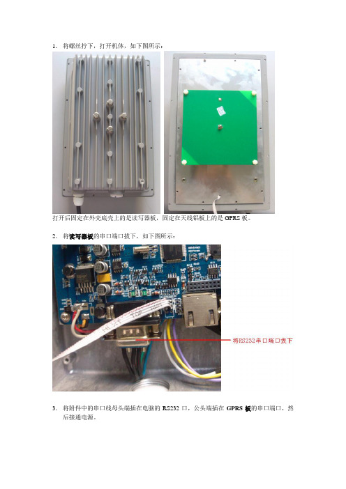
1.将螺丝拧下,打开机体,如下图所示:打开后固定在外壳底壳上的是读写器板,固定在天线铝板上的是GPRS板。
2.将读写器板的串口端口拔下,如下图所示:3.将附件中的串口线母头端插在电脑的RS232口,公头端插在GPRS板的串口端口,然后接通电源。
4.运行GPRS参数设置软件中的执行文件“”。
将弹出主界面对话框,如图:1.1通讯连接点击“系统管理”下拉菜单中的“通讯连接”,如图:将弹出下图对话框:“通讯串口”选择电脑与设备连接的串口号,通讯波特率选择设备所设置的波特率,出厂设置为57600。
选择后点击“确定”按钮。
如设置正确,则主界面第一个指示灯将变亮。
1.2通讯参数在主界面中点击“设备参数设置”菜单中的“通讯参数”,将弹出下图对话框:设备通讯地址是指设备的ID号,用来区分是哪台设备传到服务器上的数据。
其他参数不需修改。
1.3GPRS参数在主界面中点击“设备参数设置”菜单中的“GPRS参数”,将弹出下图对话框:服务提供商:是指设备里使用的SIM卡的运营商APN接入点;IP地址与端口:是指接收数据用的服务器的IP地址和接收端口,其中接收端口使用5600,不需修改;心跳时间:是指心跳包发送的时间间隔。
输入参数后点击“下载参数”。
5.将设备断电。
6.插入SIM卡,如下图所示:7.将刚刚拔下的读写器板的串口端口接上,拧上外壳螺丝即可。
8.将设备上电,运行后台管理软件。
如下图所示:在“当天GPRS实时通信记录”里,可看到当天的GPRS原始记录。
在“接收标签记录”里,可看到设备ID、标签信息、读取时间等信息。
在“垃圾桶登记”里,可将标签信息与垃圾桶信息进行绑定录入。
采用噪声消除技术的3~5GHz CMOS超宽带LNA设计

l s h n 0. B,a ma i m o s g r f2. B,a d a n u d o d ri tr e tpon f 一1 9 d esta 7 d x mu n ie f u e o 9 d i n n i p t3r r e n e c p i to 2. Bm.Th e wh l ic i i t o s mp i n o 0. ie c r u t s wih c n u to f2 5 mW n e 8 V ig e s p l . u d ra 1. sn l u p y Ke r y wo ds:n ie c n e i g;UW B;l w os mp i e ;s n —e d c os a c ln o n ie a lf r hu tf e ba k i
S C 0 1 m MOS p o e s i c rid o t T e r s l ft e smu a in s o h t h 1 s l s h n MI . 8一 RF C r c s s are u . h e u t o h i l t h w t a ,t e Sl i e s t a s o
中图分 类号 : N 2 . T 72 3
文献 标识 码 : A
文章 编号 :0 5— 4 0 2 1 )3— 2 0- 5ຫໍສະໝຸດ 10 99 (00 0 0 9 0
华为OTN设备OSN8800
3.1 组网应用........................................................................................................................................3-1 3.2 波长和业务调度 .............................................................................................................................3-1
华为专有和保密信息 版权所有 © 华为技术有限公司
iii
OptiX OSN 8800 I 智能光传送平台 产品概述
目录
目录
1 产品定位和特点 ............................................................................................................ 1-1
optixosn8800i应用于国家级干线省级干线作长距离大容量传输可以最大程度地满足运营商超大容量和超长距离传输的需求并且为运营商的多业务运行及未来网络升级扩容提供了稳定的平台
资料编码
OptiX OSN 8800 I 智能光传送平台 V100R002C00
产品概述
文档版本 发布日期
_MTK校准配置文件参数详细说明要点

_MTK校准配置文件参数详细说明要点4.1 INI 文件的介绍:4.1.1[射频功能组的复位]下面是setup INI文件中定义的项目。
GSM900 Sig = 1GSM1800 Sig = 1GSM1900 Sig = 1GSM900 NSig = 1GSM1800 NSig = 1GSM1900 NSig = 1通常设置为1,指在对CMU200设置之前对设备进行复位,为0时不复位。
4.1.2 系统设置:setup INI文件中定义的项目:External Reference Clock = 0 默认值为0,指使用CMU200输出的参考时钟,为1时使用外部参考时钟。
CMU Base GPIB Address = 20CMU的GPIB地址的设置,要与软件对应。
Instrument = "CMU200"使用的设备为CMU200Power Supply Address = GPIB0::5::INSTR电源地址的设置使用Kei230x时,应为Power Supply Address = 5CMU RF Port = 2CMU200使用的射频端口设置Test Mode = 0设为0指需要手动对设备进行初始化,1指在综测时软件将自动对设备进行初始化,2指在校准时软件将自动对设备进行初始化,3指在校准和综测联合测试时软件将自动对设备进行初始化FDM database file = "c:\\\\Program Files\\\\MTK_atedemo\\\eport\\\\BPLGUInfoCustom" Database 文件的存放路径,必须与手机软件对应Calibration file = "c:\\\\Program Files\\\\MTK_atedemo\\\\MTKCAL_6205B.INI"校准初始默认值设置文件的路径Config file = "c:\\\\Program Files\\\\MTK_atedemo\\\\meta_6205B.CFG"关于校准的设置,如校准的信道,限制的最大、最小值Report file path = "c:\\\\Program Files\\\\MTK_atedemo\\\eport_6218B"测试报告的存储路径Database file = "c:\\\\Program Files\\\\MTK_atedemo\\\\Report_Statistics\\\\6218B_statistics.xl s" 测试结果文件的存放路径IMSI = "001010123456789"SIM卡中的IMSI号的设置POWER ON AFTER CHANGE = 1联合测试时,如果设备改变不同状态时较慢,则设置为1Stability Count = 1循环测试的次数设置Fixture COM port = 1串口地址设置System Cable Loss Calibration = 0校准系统的线损选择4.1.3呼叫建立设置Setup Network = 1建立呼叫时的网络设置,1指GSM频段,2指DCS频段,3指PCS频段GSM Call Setup Channel = 1建立呼叫的信道号设置GSM BCCH Channel = 32广播控制信道的设置DCS Call Setup Channel = 512 DCS建立呼叫的信道设置DCS BCCH Channel = 700DCS广播控制信道的设置PCS Call Setup Channel = 512 PCS建立呼叫的信道设置PCS BCCH Channel = 700PCS广播控制信道的设置GSM850 Call Setup Channel = 128 GSM850建立呼叫的信道设置GSM850 BCCH Channel = 128 GSM850广播控制信道的设置BCCH RF LEVEL = -60下行广播控制信道电平BS TCH LEVEL = -80.5基站业务信道电平Triple Band = 0设置为1时要进行PCS的测试DCS Band = 1为1指综测时要测DCSGSM Band = 1为1指综测时要测GSMGSM850 Band = 0为1时,综测要测GSM850 GPRS TEST = 0为1时要进行GPRS的测试4.1.4 信令测试Power Measment Burst = 10定义功率测试时,要测的Burst的数量Average Burst Power = 1为1指要进行平均功率的测试Peak Burst Power = 1为1指要进行峰值功率的测试PVT Match = 1为1指进行功率时间模板测试Modulation Measment Burst = 10定义调制频谱测试时所要测试的Burst数量Phase Error Peak = 1为1指要进行相位峰值误差的测试Phase Error RMS = 1为1指要进行相位均方值误差的测试Frequency Error = 1为1指要进行频率误差的测试ORFS MOD Burst = 10定义调制频谱测试时,所要测试的Burst的数量Spectrum Modulation = 1为1指要进行调制频谱的测试ORFS Switch Burst = 10定义开关频谱测试时,所要测试的Burst的数量Spectrum Switch = 1为1指要进行开关频谱的测试Rx Quality = 0是否进行接收质量的测试RX Level = 0是否进行接收电平的测试RFER = 0是否进行误码率的测试BBB = 0是否进行Bust By Burst的误码率测试GSM Rx Meas Level = -100定义GSM测试误码率时的下行功率DCS Rx Meas Level = -100定义DCS测试误码率时的下行功率PCS Rx Meas Level = -100定义PCS测试误码率时的下行功率Rx RFER Burst = 128定义测试时的Burst数量Rx BBB Burst = 88定义Bust By Burst的误码率测试时,要测的Burst数量GSM Output Loss = 0.6GSM输出补偿设置GSM Input Loss = 0.6GSM输入补偿的设置DCS Out Loss = 1.2DCS输出补偿的设置DCS Inp Loss = 1.2DCS输入补偿的设置PCS Out Loss = 1.3PCS输出补偿的设置PCS Inp Loss = 1.3PCS输入补偿的设置Location update timeout = 50位置更新的延时设置Timing Error Limit = 5(bit)时间提前量的限制设置RX Level Limit = 27接收电平的限制设置RX Quality Limit = 3接收质量的限制设置Stop Condition = 0停止条件的设置,为0指无论中间的测试项目是否通过,都要继续进行测试,直到测试结束,为1指当有测试Fail的项目时,则停止测试Version New = 0当使用的综测仪的版本大于3.5时,或RAM>256M时,可以设为1,以设置其进行并行的测试,旧版本设为1时将增加测试时间Final Test With Calibration = 1设为1指进行综测和校准的联合测试Wireless Test = 0为1指进行耦合测试Get Barcode = 1读取并检查板测状态RX ClassII Limit = 1.5接收误码率ClassII的限制设置RX ClassIb Limit = 1.5接收误码率ClassIb的限制设置Default Test Items = 1综测提供了两种模式,为1时,将按照[Signalling Measurement]中的定义进行测试,为0时将按照[GSM xx]中的设置进行测试Check BarCode Delay = 15.0检测板号延时设置(综测前检测板测是否通过时,要进行板号的读取)Handover Delay Time = 0.5测试频段Handover的延时设置BER MEAS MODE = 0为0时进行单时隙的测试,为1时将进行连续时隙的测试BER Continuous Meas Delay = 1.5定义Ber连续测试模式的测试延时Mobile Report RxQ Delay = 1.5接收质量测试的延时设置,(延时以便得到正确的移动台测试值)MT Call = 0为0时手机将拨号112以进行呼叫建立,为1时,指设备将呼叫移动台进行通信连接GSM850 Rx Meas Level = -100当“default testing items”为1时,ATE将使用此值进行BER的测试6218B Normal Baud Rate = 115200定义6218B的通信波特率6205B Normal Baud Rate = 57600定义6205B的通信波特率RX Level Limit MAX = 31接收电平的最大值设置4.1.5校准设置GSMN OUT LOSS = 0.6非信令模式下GSM的输出损耗设置GSMN INP LOSS = 0.6非信令模式下GSM的输入损耗设置DCSN OUT LOSS = 1.2非信令模式下DCS的输出损耗设置DCSN INP LOSS = 1.2非信令模式下DCS的输入损耗设置COM PORT = 4串口端口设置Auto Barcode = 0为1时,软件将自动生成板号Auto Barcode Step = 1板号自动生成时的增加步长设置ADC Calibration = 0为1将进行ADC的校准Frequency Bank with PCS = 0定义是否进行PCS频段的校准BB Chip Type = "6205B"定义芯片类型CO GSM900 = 70从CFG文件中读取GSM校准信道的值CO DCS1800 = 700从CFG文件中读取DCS校准信道的值CO PCS1900 = 660从CFG文件中读取PCS校准信道的值PCSN OUT LOSS = 1.3设置非信令模式下测试PCS时的输出线损PCSN INP LOSS = 1.3设置非信令模式下测试PCS时的输入线损Enter META Mode Timeout = 10000设置进入META模式的延时Enter META Timer Delay = 2.0校准时,当电源控制异常时,可以调整此项设置AFC Calibration = 1为1时将进行AFC校准Pathloss Calibration = 1为1时将进行路径损耗校准APC Calibration = 1是否进行APC校准APC Check = 1为1时将进行APC的检测Frequency Bank with GSM850 = 0为1时将进行GSM850的校准Frequency Bank with GSM900 = 1为1时将进行GSM900的校准Frequency Bank with DCS1800 = 1为1时将进行GSM1800的校准Add Calibration Status = 1为1时将把校准结果加入条码的60,61位如:PASS : char[60]=’1’ , char[61]=’0’FAIL : char[60]=’0’, char[61]=’1’4.1.6 IMEI设置Scan IMEI = 0为1时,可以使用扫描仪扫描条码,软件会将IMEI号写入手机4.1.7综测发射测试检测:下面是CFG文件中定义的综测和校准PCL限制表:GSM900_MAX_P = "6.0,8.0,10.0,12.0,13.8,15.8,17.8,19.8,21.8,23.8,25.8,27.8,29.5,31.0, 32.9,"GSM900_MIN_P = "4.0,6.0,8.0,10.0,12.5,14.5,16.5,18.5,20.5,22.5,24.5,26.5,28.5,30.0,3 1.7,"DCS1800_MAX_P = "2.0,3.5,5.0,7.0,9.0,11.0,12.5,14.5,16.5,18.5,20.5,22.5,24.5,26.5,28. 0,31.0,"DCS1800_MIN_P = "0.0,1.5,3.5,5.0,7.0,9.0,11.5,13.5,15.5,17.5,19.5,21.5,23.5,25.0,27.0, 28.7,"PCS1900_MAX_P = "0.5,2.5,4.5,6.5,8.5,10.5,12.5,14.5,16.5,18.5,20.5,22.5,24.5,26.5,28. 5,30.5,"PCS1900_MIN_P = "-0.5,1.5,3.5,5.5,7.5,9.5,11.5,13.5,15.5,17.5,19.5,21.5,23.5,25.5,27.5,2 9.5,"频率和相位误差的限制表:GSM_Freq_Error_Limit = 90DCS_Freq_Error_Limit = 180PCS_Freq_Error_Limit = 190Phase_Error_Peak_Limit = 20Phase_Error_RMS_Limit = 5Spectrum due to switching enable = "1,0,0,1,"开关频谱和调制频谱的偏移量的定义:"1,0,0,1," 指使用+/- 400k 和+/-1.8M的偏移量进行测试Spectrum due to Switching +400kHz= -31.182460Spectrum due to Switching -400kHz= -29.590330Spectrum due to Switching +600kHz= -35.207820Spectrum due to Switching -600kHz= -32.279390Spectrum due to Switching +1.2MkHz= -34.092160Spectrum due to Switching -1.2MkHz= -38.503780Spectrum due to Switching +1.8MHz= -43.583010Spectrum due to Switching -1.8MHz= -46.116880Spectrum due to modulation enable = "0,0,0,1,0,0,0,0,0,0,1,"Spectrum due to Modulation +100kHz= -8.557312Spectrum due to Modulation -100kHz= -8.777496Spectrum due to Modulation +200kHz= -34.214780Spectrum due to Modulation -200kHz= -34.015660Spectrum due to Modulation +250kHz= -39.874850Spectrum due to Modulation -250kHz= -38.849580Spectrum due to Modulation +400kHz= -61.613100Spectrum due to Modulation -400kHz= -62.010590Spectrum due to Modulation +600kHz= -66.382050Spectrum due to Modulation -600kHz= -66.253600Spectrum due to Modulation +800kHz= -66.471500Spectrum due to Modulation -800kHz= -67.809330Spectrum due to Modulation +1MHz= -68.384120Spectrum due to Modulation -1MHz= -68.194400Spectrum due to Modulation +1.2MHz= -69.887570Spectrum due to Modulation -1.2MHz= -71.136630Spectrum due to Modulation +1.4MHz= -73.157710Spectrum due to Modulation -1.4MkHz= -72.516720Spectrum due to Modulation +1.6MHz= -74.163570Spectrum due to Modulation -1.6MHz= -76.117770Spectrum due to Modulation +1.8MHz= -76.022610Spectrum due to Modulation -1.8MHz= -78.223210Spectrum due to switch limit = "-10.0,-10.0,-21.0,-21.0,-21.0,-21.0,-24.0,-24.0,"开关频谱的限制值Spectrum due to modulation limit Line0001 ="0.5,0.5,-30.0,-30.0,-33.0,-33.0,-55.0,-55.0,-60.0,-60.0,-60.0,-60.0,-60.0,-60.0,"调制频谱的限制值4.1.板号Barcode = "S4716A0007 00"定义板号的起始值Barcode Limit = "MT012345678901234569"滤除未定义的板号,检测写入的板号位数。
ISP图像传感器原理
ISP图像传感器原理1、Color Filter Array — CFA随着数码相机、手机的普及,CCD/CMOS 图像传感器近年来得到广泛的关注和应用。
图像传感器一般都采用一定的模式来采集图像数据,常用的有 BGR 模式和 CFA 模式。
BGR 模式是一种可直接进行显示和压缩等处理的图像数据模式,它由 R( 红)、G( 绿) 、B( 蓝) 三原色值来共同确定1 个像素点,例如富士数码相机采用的SUPER CCD 图像传感器就采用这种模式,其优点是图像传感器产生的图像数据无需插值就可直接进行显示等后续处理,图像效果最好,但是成本高,常用于专业相机中。
一般数码相机的传感器(CCD 或 CMOS)约占整机总成本的10%~25%,为了减少成本,缩小体积,市场上的数码相机大多采用CFA 模式,即在像素阵列的表面覆盖一层彩色滤波阵列(Color Filter Array,CFA),彩色滤波阵列有多种,现在应用最广泛的是Bayer 格式滤波阵列,满足 GRBG 规律,绿色像素数是红色或蓝色像素数的两倍,这是因为人眼对可见光光谱敏感度的峰值位于中波段,这正好对应着绿色光谱成分。
上图就是一个采用CFA 模式的图像传感器,有效分辨率为 640 x 480,该模式图像数据只用 R、G、B 3个值中的1 个值来表示 1 个像素点。
这样一来每个像素点只能捕获三基色 R,G,B 中的一个,而缺失另外两个颜色值,这时候得到的是一幅马赛克图像。
为了得到全彩色的图像,需要利用其周围像素点的色彩信息来估计出缺失的另外两种颜色,这种处理叫作色彩插值,也称作彩色插值或去马赛克。
上图是一个8 x 8像素大小的 CFA 模式图像数据阵列,图中 1 个方格表示 1个像素,R、G、B 的数字下标表示其在 8 x 8 图像阵列中的位置。
由于CFA 模式所采用的图像颜色滤波阵列结构相对简单,并且所得到的图像数据仅仅是原始图像全部三原色信息的1 / 3 的数据,因此成本较低。
5G扫频仪测试指导手册
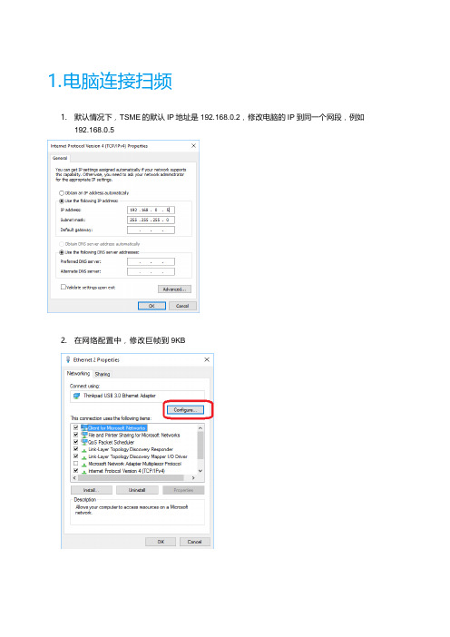
1.电脑连接扫频1.默认情况下,TSME的默认IP地址是192.168.0.2,修改电脑的IP到同一个网段,例如192.168.0.52.在网络配置中,修改巨帧到9KB3.检查防火墙如果后续软件ROMES链接不上扫频仪,还需要关闭防火墙2.检查仪器的Option1. 下载TSME Device Managerhttps:///software/tsme/ 选择下载R&S®TSME Device Manager2.安装完成后,在开始程序中 R&S TsmeTools下面找到TsmeDeviceManger打开3. 在Option 中查看License情况,如果过期请把仪器背后的编号给我3.检查Dongle的Option 1. 在开始菜单中选择License Server GUI2. 在弹出的对话框中点击右下侧的对话框3. 如果显示如下图所示,表示没有过期4.Romes 安装1. 在安装文件的Romes文件夹下面,找到Romes_setup-xx-x.exe 文件双击安装2. 选择安装项目3. 选择安装的制式4. 如果没有.dat license文件就不需要安装5. 同样如果没有.dat license文件就不需要安装6. 没有就不用安装7. 在第六步点击Install->OK 开始安装5. 5G NR 配置1. 安装完成后,插上dongle,打开软件例如: ROMES4 18.2 Measurement2. 如果软件打开时候出现下面提示,表示Romes dongle过期或者没有插Romes dongle,点击Yes进入软件可以回放,但是不能测试3. 点击start开始4. 如果能正确加载扫频仪,在左侧栏框里面点击device,会有能测试的模式,如果没有任何信息,表示仪器没有加载上去,重新配置环境,点击刷新按钮测试:5. 进入Hardware->Add/Remove6. 展开tsme,双击要测试的项目,例如5G NR,点击添加按钮7. 点击Connect连接扫频仪8. 连接好后如下图9. 如果需要添加其他制式,同样的方法添加(GPS在Navigation里面)10. 现在重新点击Hardware,发现多了我们添加的三个项目,点击R&S LTE Scanner配置11. 选择LTE配置,输入频点,速度,如果需要更多配置,选择Customer, 点击OK完成配置12. 选择5G NR配置,在Advanced上选择Open13. 在Expert Input Mode上打勾选中14. 输入正确的参数,包括SSB中心频点,SSB Patten, SSB Period等15. 开始测试16. 在View中可以看不同的视图17. 测试完成,停止测试。
【精选】5G终端无法驻留解决步骤
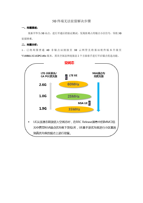
5G终端无法驻留解决步骤一、问题描述:某新开华为5G站点,进行开通后的验证测试,发现很难占用锚点小区信号,导致5G 驻留困难。
二、问题分析:1、已将周围普通4G非锚点站割接至5G云网管且将基站软件版本升级至V100R015C10SPC160e版本,需从空闲态和连接态2个方面着手进行开启锚点优选功能。
2、锚点优选相关参数配置2.1 打开NSA算法开关和锚点选择开关(针对锚点小区)MOD NSADCMGMTCONFIG: LocalCellId=*,NsaDcAlgoSwitch=NSA_DC_CAPABILITY_SWITCH-1&NSA_PCC_ANCHORING_SWITCH-1;2.2、打开锚点选择开关(针对非锚点小区)MOD NSADCMGMTCONFIG: LocalCellId=*, NsaDcAlgoSwitch=NSA_PCC_ANCHORING_SWITCH-1;2.3、针对锚点设置优先级,非锚点设置优先级为0MOD PCCFREQCFG: PccDlEarfcn=1300, NsaPccAnchoringPriority=7;MOD PCCFREQCFG: PccDlEarfcn=其他非锚点, NsaPccAnchoringPriority=0;2.4、配置SCG频点,ScgDlArfcn NR侧提供ADD NRSCGFREQCONFIG: PccDlEarfcn=1300,ScgDlArfcn=509004, ScgDlArfcnPriority=1,NrB1TimeToTrigger=512MS;2.5、NSA用户专用PCC锚点A1门限(所有小区)MOD ENBCELLRSVDPARA: LocalCellId=xx, RsvdU8Para35=30;按照以上参数配置完成后,进行现场测试,发现仍无法及时顺利占用5G.三、解决步骤:1、查询锚点DC功能及锚点优选功能开关设置情况NSA DC能力及NSA锚点选择开关均已开启。
HSDPA-throughput 步骤
1,先连接GSM850,具体设置如下图。
具体要求:连接上CMU500后,调整手机在屏蔽盒中的位置
并且在6~7之间),使手机此时的5级功率在32.5~33,并且RX LEVEL在25~26。
固定此时位置不动!如下图2 2,在保持手机在屏蔽位置不动的情况下将综测仪切换到WCDMA的信令测试界面。
在主界面设置频
RMC+HSPA,TEST MODE设置为LOOP MODE 1 RLC,且补偿要与GSM850信令测试时保持一致。
如图:
3.打开WCDMA Signaling,开机注册;
4.注册成功后,先不要建立连接。
按屏幕右上方的 WIRZARD 菜单,进入Application Wizarc,选红色方框中的M
5.建立通信连接(如果不行,可进手机工程模式,进入MODEM TEST,点击 INTIGRITY OFF,并重启
6.进入WCDMA RX MEAS,通过左右键选择HSDPA ACK,并打开HSDPA ACK.
7,在如下HANDOVER界面切换测试信道。
的位置(保证发射接收补偿一致,
定此时位置不动!如下图2
设置频段、损耗;并将Connect type设置为:一致。
如图:
arc,选中红色方框中的MAX Throughput,并Finish
并重启手机)。
- 1、下载文档前请自行甄别文档内容的完整性,平台不提供额外的编辑、内容补充、找答案等附加服务。
- 2、"仅部分预览"的文档,不可在线预览部分如存在完整性等问题,可反馈申请退款(可完整预览的文档不适用该条件!)。
- 3、如文档侵犯您的权益,请联系客服反馈,我们会尽快为您处理(人工客服工作时间:9:00-18:30)。
A CMOS 5GHz Image-Reject Receiver Front-End ArchitectureDicle Ozis 1,2, Jeyanandh Paramesh 1,3, and David J. Allstot 1 ∗1University of Washington, Seattle, WA, 98195 2Now with Telegent Systems, Inc., Sunnyvale, CA 94085 3Now with Carnegie Mellon University, Pittsburgh, PA 15213∗Research supported by National Science Foundation contract CCR-0086032 and Semiconductor Research Corp. contract 2006-HJ-1427. J. Paramesh was supported by Graduate Fellowships from the Intel Corp.Abstract —A fully-integrated double quadrature heterodyne receiver front-end uses a two-stage Lange coupler and achieves a measured image rejection ratio > 55 dB over a200MHz bandwidth at 5.25 GHz without any tuning ortrimming. It also features 23.5 dB gain, -79 dBm sensitivity,5.6 dB SSB noise figure, -7 dBm IIP3, -18dB S 11 and 1mm x 2mm chip area in 0.18 µm CMOS. Index Terms —CMOS integrated circuits, receivers, couplers, lumped-element microwave circuits, transformers. I. I NTRODUCTIONThe repeatable image rejection ratio (IRR ) of an un-calibrated single-quadrature (SQ) receiver is limited by mismatches to 35-40dB over ~2% fractional bandwidths. In a double-quadrature (DQ) architecture [1], I/Q signals are generated in both the RF and LO paths. Consequently, I/Q errors in the two paths multiply [Eqns. (1) and (2)] so that a much higher uncalibrated IRR is obtained than with an SQ receiver. Note also that I/Q mismatches in the mixers are additive so careful layout is essential for high IRR . The overall phase and amplitude errors are:()()()()2/tan tan tan tan Mixers LO RF φφφφ∆+∆⋅∆=∆ (1) ()()()2Mixers RF LO A A A A A A (A A)∆=∆⋅∆+∆ (2)Typical DQ receivers use simple RC-based I /Qgeneration to obtain high IRR over a limited bandwidth. In contrast, the use of high-order RC polyphase networks enables high, wideband IRR , but the associated high losses mandate a large preceding gain that relegates their use to I F frequencies. This paper introduces a DQ image-reject receiver (Fig. 1) wherein two-stage Lange couplers are used for the first time in a fully-integrated 0.18µm CMOS front-end to achieve high IRR over a wide bandwidth (~200MHz @ f C = 5GHz) without calibration. Single-stage passive couplers are usually not used in the signal path due to their loss and limited bandwidth. However, the two-stage Lange coupler design described herein achieves high bandwidth with acceptable noise figure; it provides a new tool for designers to use in their quest for low-noise, low-power RF circuits and systems. These techniques arewidely applicable and this paper demonstrates their effectiveness over the 5.15-5.35 GHz band. In the 70MHz-IF architecture (Fig. 1), the RF signal is first low-noise amplified and then separated into in-phase and quadrature paths using two-stage lumped-element Lange couplers [2]. The 0.18µm CMOS chip comprises an LNA, Lange couplers, down-conversion mixers, and a frequency divider with LO buffers.II. C IRCUIT B LOCKSA. Low-Noise AmplifierThe fully-differential single-stage common-source cascode LNA uses inductive source degeneration to set Z in = 50Ω. I ts output impedance is matched to the coupler input impedance using an L-match network. High coupler characteristic impedance requires a large inductance, which leads to higher losses and a low-Q match to the LNA and vice-versa. I n view of this trade-off and to facilitate stand-alone characterization of the coupler, its impedance is also set to 50. The LNA uses symmetric inductors to save chip area and a bank of switched capacitors in the output LC-tank to match its center frequency to that of the couplers.)LO sin f t )cos f t π)Fig. 1. Block diagram of the double-quadrature image-rejectreceiver front-end.nge CouplerPower dividers and directional couplers are passive microwave components used for power division or power combining. For a 3dB coupler, the power applied to any port is split equally between a pair of output ports. Hybrid couplers and power dividers mutually isolate the output ports and preserve input and output impedance levels. Quadrature couplers provide a 90-degree phase shift between output ports. Although they are typically designed using quarter wavelength transmission lines of different types for microwave and mm wave I C applications, area savings are realized by approximating the transmission lines using lumped-element networks at lower frequencies. Because the lumped-element representation is accurate only at a single frequency, lumped-element hybrids are inherently narrow-band networks but transmission line couplers are also narrowband because the quarter-wavelength restriction is satisfied exactly only at a single frequency.Fig. 2. Two Lange Couplers are cascaded to form a two-stage Lange Hybrid.The original Lange coupler, proposed in [2] connects several coupled transmission lines in parallel to divide the input signal into I/Q components with equal power. Whereas a branch-line coupler uses only electrical (capacitive) coupling, the Lange coupler employs electromagnetic (inductive) coupling to achieve a larger bandwidth. A lumped-element Lange coupler may be synthesized by replacing the coupled lines with a transformer [3], which can be constructed compactly on-chip with low loss at 5GHz. Although the bandwidth of a single-stage Lange coupler is fairly wide, it is insufficient in this design where the image is located 140MHz from the RF carrier. Therefore,a two-stage cascade coupler (Fig. 2) is developed and optimized for amplitude and phase accuracy to maximize IRR over a wide frequency range.A single-stage Lange coupler requires a monolithic transformer with a coupling factor k = 0.707, which is very difficult to realize in a bulk CMOS technology at 5GHz. I n contrast, signal flow graph analysis and synthesis show that a two-stage Lange coupler requires only k = 0.38 for each transformer. Hence, both stages are designed as identical Lange couplers. I nductive coupling in both stages provides a larger bandwidth and occupies a smaller area; a Lange coupler can be designed using a single transformer whereas a branch-line coupler requires two separate inductors. This key circuit technique enables high IRR over the entire 5.15-5.35GHz band. A transformer layout with four-fold symmetrical windings is chosen because of the required symmetry between its primary and secondary windings. I solated ports of the Lange couplers are terminated with on-chip 50 resistors. Note that an alternative two-stage coupler is presented in [4]. I t uses a capacitively-coupled (branch-line) first stage followed by an inductively-coupled (Lange) second stage, and features cancellation of phase mismatches due to the finite Q values of the passive elements. This coupler uses a transformer with k = 0.38. Due to the small k value, the overall phase response is less sensitive to variations in k; i.e., modeling errors, process variations, etc.Fig. 3. Measured image rejection ratio of the two-stage Lange hybrid with IRR > 30dB and IRR > 35dB overbandwidths of 500MHz and 275MHz, respectively.C.Double Quadrature MixerA double-balanced Gilbert-type mixer (Fig. 3) is employed in each RF path to down convert 5.15-5.35GHz RF to 70MHz IF.Fig. 4. Down-conversion mixers.To maximize power transfer, the differential RF input of the mixer is matched to 100. The output of the coupler is matched to the input RF port of the mixer using a wideband common-gate transconductance stage. The cross-coupled capacitors provide a gm-boosting mechanismthat improves noise performance without using additionalFrequency (MHz)IRR(dB)power [5]. In a standard common-gate topology, g m of the input transistor is constrained by the input impedance which imposes a tight link between noise figure and input match. The g m -boosting mechanism eases this trade-off. The negative coupling required between source and gate terminals is achieved by cross coupling. The quadrature mixers share a g m -stage to save power; hence, two g m and four switching stages are needed for DQ down conversion. A current bleeding method implemented by connecting current sources to the common-source nodes of the switching differential pairs allows independent biasing of the input and switching stages. Better switching is thus achieved with smaller transistor sizes due to the smaller bias currents of the switching transistors. This method also decreases the noise contributed by the switching stage and enables higher gain through the use of larger load resistances. As mentioned earlier, the multiplication of RF and LO amplitude and phase mismatches in the DQ front-end improves overall IRR , but mismatches in the mixers add error terms. Therefore, careful layout is critical for high IRR .Open-drain drivers buffer the outputs of the IF mixers to drive off-chip 50 measurement loads; they consume 16 mA from a 1.8V supply. Bias conditions and device sizes of the buffers are adjusted so that the measured gain of the downconverter is not affected by the 50 loading of the measurement equipment. The bias currents of buffers are mirrored from the same reference, and no tuning of buffer bias conditions is used for IRR measurements.To obtain accurate I /Q LO signals, a 2X frequency reference is divided on-chip using a master/slave D-type flip-flop. The CML latches in the divider are each biased at 4mA to ensure reliable operation from 10.44 to 10.84GHz over all process, voltage, and temperature (PVT) variations. On-chip buffers before and after the divider consume 9mA and 12mA from the 1.8V power supply, respectively. The buffers are designed to achieve adequate bandwidth versus PVT variations, and to operate with a low LO drive of < -5 dBm; they can be optimized for lower current consumption for a given system.III. M EASUREMENT R ESULTSThe DQ receiver prototype (Fig. 5) is designed for the IEEE 802.11a standard and characterized by wafer probing. The measured input return loss is < -18dB over the 200 MHz bandwidth, the gain is 23.5dB, and the SSB noise figure is < 5.6dB. Because there is no on-chip filtering, both the in-band and out-of-band IIP3 values are measured at –7dBm.Fig. 5. Chip micrograph of the image-reject receiver front-end in0.18µm CMOS.Fig. 6. Measured IRR of 15 chips (from a single wafer) for theI EEE 802.11a WLAN standard. Channel frequencies= 5.18, 5.20 ... 5.32GHz. Across the eight channels, 55dB< IRR < 63dB with µ = 58.85dB, and σ = 1.68dB.T ABLE IP ERFORMANCE C OMPARISON WITH P REVIOUS C ALIBRATION -F REE D ESIGNSRF (GHz) IF (MHz)IRR (dB) NF (dB) Gain (dB)IIP3 (dBm)-1dB Compression Point (dBm)Chip Area(mm 2) ProcessIDD @ 1.8V (mA) [6] 5.3 250 36 6.8 14 -5.5 N/A 2.4 x 1.8 0.5µm SiGe10.3[7] 5.2 30 50.2 8.516 -13 -24 2 x 1.5 0.18µm CMOS12.4This work 5.15-5.35 70 > 55 5.623.5 -7 -182 x 10.18µm CMOS 20 (LNA+Mixers)Channel numberI R R (d B )MixersLN Lange Coupler 2 mmMixers LNA Lange CouplersLO buffers& Frequency dividerinput 1 mmFig. 7. An instrumentation amplifier is connected after the I F output for sensitivity measurements.To measure IRR, sensitivity, and 802.11a-specific performance, the 70MHz IF outputs are digitized using a four-channel sampling oscilloscope with 8-bit ADCs. The digital data is fed into a vector signal analyzer that implements the digital 802.11a demodulation in software. With this setup, the measured results show IRR > 55dB without calibration for 15 samples over a wide bandwidth (~200MHz) with insensitivity to process variations and device mismatches (Fig. 6).The measurements are repeated for all data rates and coding schemes specified for 802.11a. To facilitate comparison with previous analog transceivers that derive the sensitivity from the required optimum SNR, we define sensitivity as the input power for which EVM < -18.5dB (C/I > 18.5dB) with 64-QAM OFDM @ 54Mbps. I n this test, input power is swept and EVM is measured. Because the chip features a fixed gain of 23.5dB, it is important to ensure that the sensitivity measurement is not limited by the test setup. At low input power levels, however, EVM is limited by the coarse 8-bit ADC of the digitizing scope and insufficient gain programmability of the VSA. Therefore, an instrumentation LNA is connected between the IF output of the chip and the digitizing scope (i.e., at the output as in Fig. 7) for additional gain so that ADC input range can be set to an optimal level. The measured input sensitivity is consistently -79 dBm (Fig. 8) for all 8 channels. At higher input power levels where the instrumentation LNA introduces significant distortion, the measured EVM is that of the receiver alone.VI.C ONCLUSIONSTable I compares this receiver to other calibration-free image-reject 5GHz front ends. An SQ front-end in SiGe [6] achieves IRR < 36dB; a DQ front-end in CMOS [7] achieves IRR > 50dB, but over a smaller bandwidth with a higher noise figure. Our architecture achieves IRR > 55dB over a bandwidth exceeding 200MHz with excellent overall performance, and occupies less area despite the extensive use of on-chip inductors. Hence, the two-stage Lange coupler provides accurate quadrature signal generation, and is a useful circuit technique in RF CMOS circuit and system design.Fig. 8. Measured input sensitivity of the image-reject front-end for Channel 1 at a data rate of 54Mbps. For low inputpower levels, an off-chip amplifier is cascaded with thedesigned receiver front-end.R EFERENCES[1] J. Crols and M.S.J. Steyaert., “A single-chip 900-MHzCMOS receiver front-end with a high-performance low-I F topology,”IEEE J. Solid-State Circuits, vol. 30, pp. 1483-1492, Dec. 1995.[2] J. Lange, "I nterdigitated stripline quadrature hybrid," IEEETrans. Microwave Theory Tech., vol. 17, pp. 1150-1151, Dec. 1969.[3] R. Frye, S .Kapur, and R.C. Melville, "A 2-GHz quadraturehybrid implemented in CMOS technology," IEEE J. Solid-State Circuits, vol. 38, pp. 550-555, March 2003.[4] D. Ozis and D.J. Allstot, “A CMOS 5GHz phase-compensated quadrature coupler,”IEEE Radio and WirelessSymposium, Jan. 2006, pp. 51-54.[5] X. Li, S. Shekhar, and D.J. Allstot, "Low-power GMm-boosted LNA and VCO circuits in 0.18µm CMOS," IEEEInt. Solid-State Circuits Conf., Feb. 2005, pp. 534-536. [6] J.R. Long, “A low-voltage 5.1-5.8 GHz image-rejectdownconverter RFIC,”IEEE J. Solid-State Circuit s, vol. 35,pp. 1320-1328, Sept. 2000.[7] C.-Y. Wu and C.-Y. Chou, "A 5-GHz CMOS double-quadrature receiver front-end with single-stage quadrature generator," IEEE J. Solid-State Circuits, vol. 39, pp. 519-521, March 2004.VNANF = 5.6 dB IIP3 = - 7 dBGain=29 dBNF=2.9 dBIIP3=-15 dBmInput power (dBm)EVM(dB)。