Sunplus SPHE8202V Design Guide_for_zihuan
VSC8221芯片评估板用户指南说明书

VSC8221User Guide VSC8221 Evaluation BoardContents1Revision History (1)1.1Revision 1.0 (1)2Introduction (2)3General Description (3)3.1Hardware Features (3)3.1.1Power Connections (3)3.1.2Copper Port RJ45 Connections (3)3.1.3SFP or SMA SGMII MAC Interface (3)3.1.4Switches (3)3.1.5Taitien 25 MHz Crystal (3)3.1.6External RefClk Option (4)3.1.7Silabs Microcontroller (4)3.1.8EEPROM Option (4)3.1.9CMODE Pins (4)3.1.10CLOCKOUT SMA (4)3.2Software Requirements (4)4Quick Start (5)4.1Board Configuration (5)4.1.1Clock and Reset (5)4.1.2Power Up (5)4.2GUI and Driver Installation (5)4.3Using the GUI (6)4.4Test Cases (7)4.4.1CAT5 to 802.3z Serdes with Clause 37 AutoNeg Detection (7)4.4.2CAT5 to SGMII with Modified Clause 37 AutoNeg Disabled (8)4.5Useful Registers (8)4.5.1Ethernet Packet Generator (8)4.5.2Far-End Loopback (8)4.5.3Near-End Loopback (8)5Additional Information (9)1Revision HistoryThe revision history describes the changes that were implemented in the document. The changes arelisted by revision, starting with the most current publication.1.1Revision 1.0Revision 1.0 was the first release of this document. It was published in December 2013.2IntroductionThe VSC8221 device is a low-power, Gigabit Ethernet transceiver suited for Ethernet Switches with SGMII/SerDes MAC interfaces, Media Converter applications, and SFP/GBIC modules. The VSC8221 device alsoincludes Vitesse’s VeriPHY Cable Diagnostics feature.This document describes the operation of the VSC8221 Evaluation Board (VSC8221EV). The Quick Startsection describes how to install and run the graphical user interface (GUI) to fully control the evaluationboard.Figure 1 • VSC8221EVThe following reference documents provide additional information about the operation of the VSC8221evaluation board.VSC8221 DatasheetVSC8221 Evaluation Board GUIVSC8221 Evaluation Board Schematics3General DescriptionThe VSC8221EV provides the user a way to evaluate the VSC8221 device in multiple configurations. OneRJ-45 connector is provided for the copper media interface. The MAC interface is provided via SMAconnectors or alternatively through an SFP connector.The VSC8221’s internal registers are accessed via the MDIO bus from an external microcontroller drivenby an external PC via USB. The accompanying GUI enables the user to read and write the deviceregisters. Alternatively, the VSC8211EV also has the capability to configure the VSC8221 through anEEPROM or Rabbit microcontroller (not-provided).The evaluation board has the option to use VSC8221’s internal on-chip oscillator by connecting a 25MHzcrystal to XTAL1 and XTAL2 or an external reference clock signal through the REFCLK SMA (J11).3.1Hardware Features3.1.1Power ConnectionsFor convenience, the evaluation board runs off a single +5VDC power supply. On board DC-DCconvertors create the +3.3VDC rail for the board and optional +1.2VDC rail. Power is supplied to theupper right corner of the board. Power can be applied either to the 5.5 x 2.1 mm barrel connector (J20)or the banana receptacles (J21 and J15). The slide switch (SW-4) selects between the external (on-board) and internal (on-chip) regulator option. J22 is an optional monitor point for the 1.2 V rail. Whenpowered by a bench top supply the board may draw up to 3 A maximum, module included.3.1.2Copper Port RJ45 ConnectionsThe RJ45 copper media PHY port (J1) uses a generic RJ45 jack with a discrete Pulse H5008 magnetictransformer.3.1.3SFP or SMA SGMII MAC InterfaceThe default MAC interface is provided through an SFP port connector. When using the SFP port, theSigDet polarity must be swapped in the VSC8221. See register 19E.0. Note that the transmit disablesignals (TXDIS) are connected to ground, thus the laser is always turned on.An optional MAC interface through SMA connectors may be enabled by removal and re-soldering the ACcoupling caps (C7–C10) from horizontal to vertical position.3.1.4SwitchesThere are two switches on the board:SW4 to select between utilizing a +1.2V internal regulator or external regulator. The default optionfor the board is to use the external regulator.SW2 allows the user to select the mode of the EECLK/PLLMODE pin. In the on position a logic highvoltage (pull-up resistor) configures the device for a 125MHz reference clock while a logic lowvoltage (pull-down resistor) selects a 25MHz reference clock option. This is a momentary ON switchwhich requires the user to hold it in the on position for 3 seconds during board power up or devicereset.3.1.5Taitien 25 MHz CrystalThe evaluation board is shipped configured to use the VSC8221’s internal on-chip oscillator. The jumperon J12 should be installed in the XTAL (left) position, and the jumper on J24 should be installed in thePLL enable or VCC (right) position.Note: Review the required action for SW2 mentioned above.1. 1.2.3.1.6External RefClk OptionThe user may choose to provide an external PHY REFCLK via the SMA connector (J11). The user must configure the device by installing a jumper on J24 in the PLL disable or ground (left) position and installing a jumper on J12 in the SMA (right) position.3.1.7Silabs MicrocontrollerA Silabs F340 microcontroller is included to facilitate a software interface to the registers on the VSC8221through a USB port.3.1.8EEPROM OptionThe user may choose to configure theVSC8221 via an EEPROM load. In order to program the EEPROM properly, pull-up or pull-down resistors must be configured for either R7 – R9 or R15 – R17. See Section 19 of the datasheet regarding to EEPROM programming requirement.3.1.9CMODE PinsOn the lower center of the board, there is an option to change the CMODE pin pull-up or pull-down resistors, R6, R12 – R14, and R18 – R21. See Section 18 of the datasheet for the detail on how toprogram the desired operating condition parameters through the CMODE configuration bits and how to choose the value of each CMODE pull-up or pull-down resistor.3.1.10CLOCKOUT SMAThe user should observe a 125MHz output clock through this SMA if the internal PHY PLL is operating properly.3.2Software RequirementsThe VSC8221 GUI can be loaded on to any PC or laptop that complies with the following requirements:The PC must run a recent version of MS-Windows. According to the Microsoft website, the following operating systems can run .NET based applications:Windows 2000Windows XP Windows Vista Windows-7Note: The GUI may be slower when run on Windows 2000 operating system.Hardware requirements must be considered when deploying/installing .NET applications. The minimum hardware requirement for a system running a .NET application is a Pentium 90MHz with 32 MB of RAM. For best performance, a newer system is recommended along with a minimum of 1 GB of RAM.If the .NET Framework 2.0 is not already installed, it may be obtained from the following link: /downloads/details.aspx?FamilyID=0856EACB-4362-4B0D-8EDD-AAB15C5E04F5&displaylang=en4Quick Start4.1Board ConfigurationPrior to powering the board, ensure that the jumpers and switches are in the following positions.Table 1 • Switch and Jumper ConfigurationSwitch/Jumper PositionJ19 (MDC)Jumper installed connecting F340 MDC to DUT MDCJ19 (MDIO)Jumper installed connecting F340 MDIO to DUT MDIOJ14 (TRSTB)Jumper installed connecting to GND. This is not requiredwhen R48 is installed.J12 (XTAL1/REFCLK)Jumper installed connecting center pin to XTAL.J24 (PLL ENABLE/DISABLE)Jumper installed connecting center pin to PLL ENABLE.SW2Hold in the left position during power-up and reset.SW4Slide to the left to use the on-chip regulator.4.1.1Clock and ResetPower must be applied and the clock (either 25 MHz or 125 MHz) must be active at the correctfrequency for the prescribed period of time in the datasheet before the RESETB pin is released.PLLMODE and OSCDISB pins are sampled during the device power-up or on assertion of RESETB pin.The board will be shipped configured for use of the 25 MHz crystal thus OSCDISB must be pulled up andPLLMODE must be pulled down during power-up or assertion of RESETB by setting J24 to the PLL enableposition and holding SW-2 in the 25 MHz position upon power-up.4.1.2Power UpProvide +5VDC to the board by plugging in the power cable (included in the kit) to J20. Two green LEDsshould illuminate: D12 on the left side of the board indicating +3.3VDC present and D11 on the right sideof the board indicating +1.2VDC present.4.2GUI and Driver InstallationDownload the VSC8221EV GUI from Vitesse’s website onto a PC that has a USB port. Install the GUI bylaunching the setup.exe file. Once installed, connect the USB cable between the USB port of the PC andthe USB connector (J16) on the evaluation board. Ensure the MDIO and MDC jumpers are properlyplaced from DUT to F340 on J23 to establish the connection between the VSC8221’s SMI pins and theSiLab F340.USB communication is assisted by the Silabs USBXpress® drive. If not present on the PC, the user willneed to download the USBXpress Development Kit from the Silicon Labs website (URL: http://www./products/mcu/Pages/USBXpress.aspx). Follow the installation directions after downloading the development kit.To ensure the USBXpress driver is installed and properly recognizing the evaluation board, go to ControlPanel and click on System>Hardware>Device Manager, and inspect the Universal Serial Bus controllerslisted to see if “USBXpress Device” appears. The following figure shows that the PC recognizes that aUSBXpress Device is connected.Figure 2 • USBXpress as Seen from the Device Manager Window4.3Using the GUILaunch the GUI either by clicking on the Desktop shortcut or clicking on the “Start – Programs – VitesseSemiconductor Corp - VSC8221_Evaluation_System” icons. The initial window will detect the attachedUSB devices automatically. The following figure shows a typical EVB Connection window.Figure 3 • Connection WindowThe EVB serial number should appear. If not, click on “Scan For USB Devices.” Select that EVB serialnumber then click “Launch GUI”. The Register List window will appear as shown in the following figure.1. a. b. c. d.Figure 4 • Register List WindowVerify that the device is up and running by reading MII Register 0. It should read back 0x1040. Reading back “0000” or “FFFF” (all 0’s or all 1’s) indicates a problem.To read or write the extended MII registers click on the ExtMII tab.An initialization script may be used to configure multiple VSC8221 registers. The initialization script is simply a text file which contains a list of registers to be written. Select the Device item on the top pull down menu area and click on Load-All-Registers option. A pop-up window will appear. Navigate to and select the desired script to be loaded.As per Section 31.1 of the datasheet, there are a number of internal registers that must be changed from their default value during device initialization. Use this method to initialize the device by loading “vsc8221_workaround31_1.txt” included in the GUI package under the Script/ directory. GUI Setup4.4Test Cases4.4.1CAT5 to 802.3z Serdes with Clause 37 AutoNeg DetectionAfter power-up or reset, the VSC8221 will operate at CAT5 to 802.3z Serdes with clause 37 Auto Negotiation Detection mode. An SFP loopback module enables MAC side SGMII loopback. 1G Ethernet received by the VSC8221 RJ-45 port is routed through the VSC8221 and looped back via SGMII through the SFP Electrical Loopback module.Set up the copper Ethernet traffic source (e.g., IXIA or Smartbits).Connect an Ethernet cable to an RJ-45.Plug in a SFP loopback module.Monitor the link-up bit in MII Register 1, bit 2 (MII 1.2), read twice to update. Traffic should now be flowing.1. 2. 3. 4. 5. 6. 4.4.2CAT5 to SGMII with Modified Clause 37 AutoNeg DisabledTo configure the device for Clause 37 Auto-negotiation disabled, perform these steps:Set up the copper Ethernet traffic source (e.g., IXIA or Smartbits).Connect an Ethernet cable to an RJ-45.Plug in a SFP loopback module.Write 0xBA20 to “MII Register” (Port 0) Reg 23 (Extended PHY Control #1).Write 0x9040 to “MII Register” (Port 0) Reg 0 (SW Reset for PHY Control setting to take effect).Monitor the link-up bit in MII Register 1, bit 2 (MII 1.2), read twice to update. Traffic should now be flowing.4.5Useful Registers4.5.1Ethernet Packet GeneratorExtMII 29E is the Ethernet Packet Generator register. Refer to datasheet for configuration options.A bad-CRC counter is in ExtMII 23.7:0. This counter will be saturate at 0xFF and is cleared when read.4.5.2Far-End LoopbackWhen MII Register 23 bit 3 is set to 1, it forces incoming data from a link partner on the media side to be retransmitted back to the link partner on the media interface.4.5.3Near-End LoopbackWhen MII Register 0 bit 14 is set to 1, the transmit data (TDP/TDN) on the MAC side is looped back onto the receive data (RDP/RDN pins) to the MAC.5Additional InformationFor any additional information or questions regarding the device(s) mentioned in this document, contactyour local sales representative.Microsemi HeadquartersOne Enterprise, Aliso Viejo,CA 92656 USAWithin the USA: +1 (800) 713-4113Outside the USA: +1 (949) 380-6100Sales: +1 (949) 380-6136Fax: +1 (949) 215-4996Email:***************************© 2013 Microsemi. All rights reserved. Microsemi and the Microsemi logo are trademarks of Microsemi Corporation. All other trademarks and service marks are the property of their respective owners.Microsemi makes no warranty, representation, or guarantee regarding the information contained herein or the suitability of its products and services for any particular purpose, nor does Microsemi assume any liability whatsoever arising out of the application or use of any product or circuit. The products sold hereunder and any other products sold by Microsemi have been subject to limited testing and should not be used in conjunction with mission-critical equipment or applications. Any performance specifications are believed to be reliable but are not verified, and Buyer must conduct and complete all performance and other testing of the products, alone and together with, or installed in, any end-products. Buyer shall not rely on any data and performance specifications or parameters provided by Microsemi. It is the Buyer's responsibility to independently determine suitability of any products and to test and verify the same. The information provided by Microsemi hereunder is provided "as is, where is" and with all faults, and the entire risk associated with such information is entirely with the Buyer. Microsemi does not grant, explicitly or implicitly, to any party any patent rights, licenses, or any other IP rights, whether with regard to such information itself or anything described by such information. Information provided in this document is proprietary to Microsemi, and Microsemi reserves the right to make any changes to the information in this document or to any products and services at any time without notice.Microsemi, a wholly owned subsidiary of Microchip Technology Inc. (Nasdaq: MCHP), offers a comprehensive portfolio of semiconductor and system solutions for aerospace & defense, communications, data center and industrial markets. Products include high-performance and radiation-hardened analog mixed-signal integrated circuits, FPGAs, SoCs and ASICs; power management products; timing and synchronization devices and precise time solutions, setting the world's standard for time; voice processing devices; RF solutions; discrete components; enterprise storage and communication solutions; security technologies and scalable anti-tamper products; Ethernet solutions; Power-over-Ethernet ICs and midspans; as well as custom design capabilities and services. Microsemi is headquartered in Aliso Viejo, California, and has approximately 4,800 employees globally. Learn more at www. .VPPD-03471。
Get格雅基于LabVIEW和DS820的多点温度测试系统—上位机部分
基于LabVIEW和DS820的多点温度测试系统—上位机部分毕业设计〔论文〕原创性声明和使用授权说明原创性声明本人郑重承诺:所呈交的毕业设计〔论文〕,是我个人在指导教师的指导下进行的研究工作及取得的成果。
尽我所知,除文中特别加以标注和致谢的地方外,不包含其他人或组织已经发表或公布过的研究成果,也不包含我为获得及其它教育机构的学位或学历而使用过的材料。
对本研究提供过帮助和做出过奉献的个人或集体,均已在文中作了明确的说明并表示了谢意。
作者签名:日期:指导教师签名:日期:使用授权说明本人完全了解大学关于收集、保存、使用毕业设计〔论文〕的规定,即:按照学校要求提交毕业设计〔论文〕的印刷本和电子版本;学校有权保存毕业设计〔论文〕的印刷本和电子版,并提供目录检索与阅览效劳;学校可以采用影印、缩印、数字化或其它复制手段保存论文;在不以赢利为目的前提下,学校可以公布论文的局部或全部内容。
作者签名:日期:学位论文原创性声明本人郑重声明:所呈交的论文是本人在导师的指导下独立进行研究所取得的研究成果。
除了文中特别加以标注引用的内容外,本论文不包含任何其他个人或集体已经发表或撰写的成果作品。
对本文的研究做出重要奉献的个人和集体,均已在文中以明确方式标明。
本人完全意识到本声明的法律后果由本人承当。
作者签名:日期:年月日学位论文版权使用授权书本学位论文作者完全了解学校有关保存、使用学位论文的规定,同意学校保存并向国家有关部门或机构送交论文的复印件和电子版,允许论文被查阅和借阅。
本人授权大学可以将本学位论文的全部或局部内容编入有关数据库进行检索,可以采用影印、缩印或扫描等复制手段保存和汇编本学位论文。
涉密论文按学校规定处理。
作者签名:日期:年月日导师签名:日期:年月日注意事项1.设计〔论文〕的内容包括:1〕封面〔按教务处制定的标准封面格式制作〕2〕原创性声明3〕中文摘要〔300字左右〕、关键词4〕外文摘要、关键词5〕目次页〔附件不统一编入〕6〕论文主体局部:引言〔或绪论〕、正文、结论7〕参考文献8〕致谢9〕附录〔对论文支持必要时〕2.论文字数要求:理工类设计〔论文〕正文字数不少于1万字〔不包括图纸、程序清单等〕,文科类论文正文字数不少于万字。
Yokogawa PH20和FU20 pH Redox和温度传感器用户手册说明书

Model PH20 and FU20pH/Redox and Temperature sensorThe PH20 is nicknamed “Tempress” because of the patented compensation for changes in the process temperature andpressure. This simple mechanical feature makes the sensor more accurate, and gives it a longer lifetime. The compensation panels flex to accommodate changes in the avoiding large differential pressures across the diaphragm. This prevents most problems associated with the reference junction. Made in chemically resistant PVDF, this all-in-one sensor has elements to measure pH, ORP and temperature. The reference system is Silver/Silver Chloride, with a double junction and a gelled electrolyte to combat pollution. The Platinum Redox electrode doubles as a solution ground, essential for uncompromising accuracy, and for sensor diagnostic measurements.The FU20 combination sensors show how Yokogawa applies the motto “Simply the Best” to sensor technology. The wide body sensors (26 mm diameter) hold four separate elements in one unbreakable PPS 40GF (RytonTM) body. Installation is simple with the integrated industrial 3/4” tapered thread. The large volume gelled electrolyte and the double junction reference system slows down depletion and poisoning therefore extending the lifetime. The system is targeted at those applications where simplicity will result in accurate and reliable pH- or redoxmeasurements. This means that in 90% of the know applications this sensor will be an excellent choice.Features• Simultaneous pH- and ORP measurement • I ntegral Pt1000 temperature element for enhanced accuracy • Available with VP connector • D ouble junction and long diffusional path for reference pollution resistance • E xtended life time by large volume of polymerized electrolyte and porous PTFE diaphragm • S olid Glass/Platinum electrode for solution ground or ORP measurement• Simple maintenance by comprehensive design • Direct in-line, immersion or off-line installation • Calibration certificate delivered with each sensorGeneralSpecificationsGeneral Specifications PH20Measuring elements: p H glass electrode and Silver/Silver chloride reference system.: P latinum electrode and Pt1000temperature sensor. Construction materialsBody : PVDFEarthing pin : Solid platinum/glassO-ring : VitonReference junction : Porous PTFECable : Coaxial with 4 extra leads Sheetmaterial : Thermoplastic rubber Functional specifications (at 25°C)Isothermal point : pH 7Reference system : Ag/AgCl with saturated KCl Glass impedance : 200 MΩ (nominal), G-glass Junction resistance : 1 to10 kΩTemperature element : Pt1000 to IEC 751 Asymmetry potential : < 15 mVSlope : > 96 % (of theoretical value) Dynamic specifications (at 25°C)Response time pH step (7 to 4): < 10 sec for 90%Response time temp. step (10°C): < 3 min for 90 %Stabilisation time (0.02 pH/10 s): < 1 minuteOperating rangepH : 0 - 14*Temperature : -10 to 105ºC (14 to 212 °F) Pressure : 0 to 10 bar ( 0 to 142 PSIG) Conductivity : > 50 µS/cmStorage temperature : -30 to 50ºC (-22 to 122 °F)The erratic trend of the standard sensor shows the progressive contamination of its reference junction. The graph indicates between 0.1 to 0.4 pH error with the conventional sensor while the readings from the PH20 are extremely stable.General Specifications FU20Measuring elements : p H glass electrode and silverchloride reference system.Platinum electrode and Pt1000temperature sensor. Construction materialsBody : R yton R4TM (PPS 40GF) with glassfillingEarthing pin : Solid platinumO-ring : NoneReference junction : Porous PTFECable : Coaxial with 4 extra leads Sheetmaterial : Thermoplastic rubber Functional specifications (at 25°C)Isothermal point : pH 7Reference system : Ag/AgCl with saturated KCI Glass impedance- Dome shape : 350MΩ, G-glass- Flat Surface : 750MΩ, G-glassJunction resistance : 0.5 to 5 kΩTemperature element : Pt1000 to IEC 751Asymmetry potential : < 15 mVSlope : > 96 % (of theoretical value) Dynamic specifications (at 25°C)Response time pH step (7 to 4): < 15 sec for 90%Response time temp step (10°C)- Dome shape : < 3 min for 90%- Flat surface : < 6 min for 90%Stabilisation time (0.02 pH/10 s): < 2 minutesOperating rangepH : 0 - 14*Temperature : -10 to 105ºC (14 to 212 °F) Pressure : 0 to 10 bar ( 0 to 142 PSIG) Conductivity : > 50 µS/cmStorage temperature : -30 to 50ºC (-22 to 122 °F)* T he pH range at room temperature is 0 -14 pH, but at high temperatures the lifetime will be seriously shortened outside 2 - 12 pH range.2GS 12B6J3-E-E3 Dimensions4Installation examples using the PH20 adapter rangeUsing the /SF4 adapter, the PH 20 can be mounted in the standard range of conductivity flow fitting (FF40..), the immersion fittings (FD40-..) and sub-assemblies (FS40..). The adapter can be mounted on the front thread, or the back thread dependent on the required insertion depth.GS 12B6J3-E-EFD40 fittings (/FPS or K1523DD)Note: old part K1523DC is not compatible with VP connector.5GS 12B6J3-E-EInstallation examples using the FU20 adapter range6Model and Suffux codesModel Suffix Option DescriptionCode codePH20 4-in-1 pH sensorMaterial -F PVDFMembrane -G Dome shapedCable length -02 2 meter-05 5 meter-10 10 meter-20 20 meter-30 30 meterTemp. element -T1 Pt1000-N -A Always -N -AOptions*/SN3 S tainless steel 3/4” NPT adapter (316L)/SR3 S tainless steel 3/4” R adapter (316L)/FN4 P VDF 1” NPT adapter/FR4 P VDF 1” R adapter/PH8 A dapter for PH8 combi sensor fittings (only)/SF4 S tainless steel adapter for FF40, FS40 and FD40 fitings/HCNF H astelloy cleaning system* Note: Option /Q: Quality Inspection certificate is always included with the product.Model Suffix Option DescriptionCode codeFU20 Wide body sensor-VP Variopin connectorCable length -03 3 meter-05 5 meter-10 10 meter-20 20 meterTemp. element -T1 Pt1000Model -NPT Dome shape model-FSM Flat surface modelOptions*/HCNF H astelloy cleaning system/FPS Adapter F*40 from noryl/NSS 1” NPT adapter, SS (316L)/NTI 1” NPT adapter, Titanium/BSS 1” BSP adapter, SS (316L)/BTI 1” BSP adapter, Titanium* Note: Option /Q: Quality Inspection certificate is always included with the product.Model Suffix Code DescriptionWU10Sensor cableConnector type -V VariopinCable type -S Single CoaxCable length -02 2 meters-05 5 meters-10 10 meters-15 15 meters-20 20 metersGS 12B6J3-E-ECleaning system for FU20 & PH20Some applications require frequent cleaning of the electrode. For these applications Yokogawa designed a chemical cleaning system that can either be used in the Yokogawa fitting range (HCN2, HCN3 or HCN4) or as back-end mounting option for the PH20 and FU20. The /HCNF option comes with a hastelloy cleaning nozzle, Stainless steel mounting (and ferrules) sets and a nylon tube of 10 meters.7GS 12B6J3-E-ESpare parts PH20, FU20 and cleaning systemPart no. DescriptionK1500EK O-rings viton 6.07x1.78 (5x2)K1500ER O-ring set Viton FF20-S22K1511DP O-rings viton 21.9x2.62 (5x2)K1511DQ O-rings EPDM 21.9x2.62 (5x2)K1547PC /FN4 for PH20K1547PD /FR4 for PH20K1547PE /PH8 for PH20K1547PG Nozzle and mounting HCN4K1547PP Spare Part EPDM spraying valves K1547QA /SN3 for PH20K1547QB /SR3 for PH20K1547QF /SF4 for PH20K1500FR O-rings Viton 29.82x2.62 (5)K1500FS O-rings EPDM 29.82x2.62 (5)K1500FT O-rings Silicon, 29.82x2.62 (5)K1520ZD Mounting nut for PS20K1523DD /FPS, FU20-mounting in F*40K1547PK Adapter 1” NPT, SS 316 for FU20K1547PL Adapter 1” BSP, SS 316 for FU20K1547PM Adapter 1” NPT, Ti for FU20K1547PN Adapter 1” BSP, Ti for FU20K1547PJ Hast. cleaning unit HCNFK1547PFNozzle and mounting HCN2/3/FAccessories Buffer powder 6C231 Buffer powder pH 1.68 ; IEC 60746-26C232 Buffer powder pH 4.01 ; IEC 60746-26C236 Buffer powder pH 9.18 ; IEC 60746-26C237 Buffer powder pH 6.87 ; IEC 60746-2Connection equipment BA10 Junction box for pH extension cables WF10-xxx-F p H signal cable with terminated ends. Specifylength in whole metersGS 12B6J3-E-ESubject to change without notice Printed in The Netherlands, 11-705 (A) ICopyright©Conventional pH (& ORP) wiringConnect the PH20 or FU20 to the EXA or EXAxt PH analyzer as shown. With this configuration, it is possible to measure ORP (or rH) at the same time (Refer to the EXA or EXAxt manual for appropriate impedance jumper and Service Code settings).Wiring for ORP measurement with pH referenceConnect the PH20 or FU20 to the EXA Glass PH analyzer as shown. Refer to the EXA manual for appropriate impedance jumper and Service Code settings.Wiring for ORP measurement with normal referenceRefer to the EXA manual for appropriate impedance jumper and Service Code settings.Wiring of the PH20 / FU20。
SPHE8203R - Des Guide

CARD Reader TVUSB 2.0CVBS/YUV/SCART(SD/MMC/MS)SPI FlashGameDVD Loader8203RICHDMI5.1CH AudioVFD/IRSPHE8203RFigure 2-2 計算特性阻抗SPHE8203RFigure 2-4 HDMI differential trace layoutSPHE8203RFigure 2-6 USB 2.0 differential trace layoutSPHE8203RR3Figure 2-8 建議系統的 Reset Circuit SPHE8203RFigure 2-10 A+5V Power(2) M+5V Power提供給 motor driver 的 power,由於為主要耗電元件,因此穩壓電容非常的重要,務必在進driver 前配置大型電解電容。
並注意此 power 分支不宜和其他 5VFigure 2-11 M+5V PowerClose to 8203RFigure 2-13 PHURF layoutFigure 2-14 高頻信號參考訊號走線計有 Vref1、Vref2等兩種參考訊號,Vref1需接Bulk and bypass 電容以保證訊號穩定性而針對VREF2,目前SPHE8203R是以一新架構來產生出所需VREF2訊號,所以在線路上請依照藍色框線內的設定值設置,其中,圖2-15中的470 ohm電阻需盡量靠近SPHE8203R擺放。
Figure 2-15 參考訊號Figure 2-16 Audio OP PowerFigure 2-18 Crystal layoutSPHE8203RFigure 2-19 Load control signals 2.13 PCB LayoutFigure 2-20 Power trace layoutFigure 2-21 Power trace with I/O connector(3) 要注意所有信號線不可有跨plane (power and ground plane) 的情形發生。
Solaris 8 (SPARC 平台版) 发行说明说明书

Solaris8(SP ARC平台版)10/00发行说明更新Sun Microsystems,Inc.901San Antonio RoadPalo Alto,CA94303-4900U.S.A.部件号码806-6267–102000年10月Copyright2000Sun Microsystems,Inc.901San Antonio Road,Palo Alto,California94303-4900U.S.A.版权所有。
本产品或文档受版权保护,其使用、复制、发行和反编译均受许可证限制。
未经Sun及其授权者事先的书面许可,不得以任何形式、任何手段复制本产品及其文档的任何部分。
包括字体技术在内的第三方软件受Sun供应商的版权保护和许可证限制。
本产品的某些部分可能是从Berkeley BSD系统衍生出来的,并获得了加利福尼亚大学的许可。
UNIX是通过X/Open Company,Ltd.在美国和其他国家独家获准注册的商标。
Sun、Sun Microsystems、Sun标志、、AnswerBook、AnswerBook2、Java,JDK,DiskSuite,JumpStart,HotJava,Solstice AdminSuite,Solstice AutoClient,SunOS,OpenWindows,XView,和Solaris是Sun Microsystems,Inc.在美国和其他国家的商标、注册商标或服务标记。
所有SPARC商标均按许可证使用,它们是SPARC International,Inc.在美国和其他国家的商标或注册商标。
带有SPARC商标的产品均以Sun Microsystems,Inc.开发的体系结构为基础。
PostScript是Adobe Systems,Incorporated的商标或注册商标,它们可能在某些管辖区域注册。
Netscape Navigator(TM)是Netscape Communications Corporation的商标或注册商标。
Silicon Labs Wi-SUN 软件开发套件和硬件产品说明书

Wi-SUN SDK 1.1.0.0 GAGecko SDK Suite 3.2July 21, 2021Wireless Smart Ubiquitous Network (Wi-SUN) is the leading IPv6 sub-GHz mesh technol-Array ogy for smart city and smart utility applications. Wi-SUN brings Smart Ubiquitous Networksto service providers, utilities, municipalities/local government, and other enterprises, byenabling interoperable, multi-service, and secure wireless mesh networks. Wi-SUN canbe used for large-scale outdoor IoT wireless communication networks in a wide range ofapplications covering both line-powered and battery-powered nodes.Silicon Labs' Wi-SUN hardware is certified by the Wi-SUN Alliance, a global industry as-sociation devoted to seamless LPWAN connectivity. Wi-SUN builds upon open standardinternet protocols (IP) and APIs, enabling developers to extend existing infrastructure plat-forms to add new capabilities. Built to scale with long-range capabilities, high-datathroughput and IPv6 support, Wi-SUN simplifies wireless infrastructure for industrial ap-plications and the evolution of smart cities.These release notes cover SDK versions:1.1.0.0 released July 21, 20211.0.1.0 released June 16, 20211.0.0.0 released May 10, 2021Compatibility and Use NoticesFor information about security updates and notices, see the Security chapter of the Gecko Platform Release notes installed with this SDK or on the Silicon Labs Release Notes page. Silicon Labs also strongly recommends that you subscribe to Security Advisories for up-to-date information. For instructions, or if you are new to the Silicon Labs Wi-SUN SDK, see Using This Release.Compatible Compilers:IAR Embedded Workbench for ARM (IAR-EWARM) version 8.50.9•Using wine to build with the IarBuild.exe command line utility or IAR Embedded Workbench GUI on macOS or Linux could result in incorrect files being used due to collisions in wine’s hashing algorithm for generating short file names.•Customers on macOS or Linux are advised not to build with IAR outside of Simplicity Studio. Customers who do should carefully verify that the correct files are being used.GCC (The GNU Compiler Collection) version 10.2.0, provided with Simplicity Studio.Contents Contents1Wi-SUN Stack (2)1.1New Items (2)1.2Improvements (2)1.3Fixed Issues (2)1.4Known Issues in the Current Release (2)1.5Deprecated Items (3)1.6Removed Items (3)2Wi-SUN Applications (4)2.1New Items (4)2.2Improvements (4)2.3Fixed Issues (4)2.4Known Issues in the Current Release (4)2.5Deprecated Items (5)2.6Removed Items (5)3Using This Release (6)3.1Installation and Use (6)3.2Security Information (6)3.3Support (7)1 Wi-SUN Stack1.1 New ItemsAdded in release 1.1.0.0•Added a new SL_WISUN_MSG_NETWORK_UPDATE_IND_ID event that is fired when the network is updated: ip address update, new primary parent or new secondary parent.•The stack library is now compiled with the preprocessor definition DEBUG_EFM_USER and provides a default implementation of assertEFM(). It will only be used if the application is also compiled with that same definition. The user can provide a custom imple-mentation. See assertEFM() documentation for more information.Added in release 1.0.0.0Wi-SUN stack and SDK initial release1.2 ImprovementsNone1.3 Fixed IssuesFixed in release 1.1.0.0710923 Fixed an issue causig the event SL_WISUN_MSG_CONNECTED_IND_ID to be fired although no new connection was established. It was fired after each network update.699627 Fixed an issue causing connections to fail after an operating class update.721399 Fixed an issue causing US-IE configuration to be invalid when excluding channels.Fixed in release 1.0.1.0701190Fixed an issue causing a parent to lose track of its child frequency hopping sequence. The child router was sending an incorrect IFSU misleading the parent router and forcing it to be one frequency hop interval late. Fixed in release1.0.0.0Wi-SUN stack and SDK initial release1.4 Known Issues in the Current ReleaseIssues in bold were added since the previous release.714402 Wi-SUN border routervery infrequently hits a hard fault. Thecommand line interface is non-responsive and the router will notadvertize anymore. Routers will eventually report a PAN timeout.1.5 Deprecated ItemsNone1.6 Removed ItemsRemoved in release 1.1.0.0•Removed internal type definitions from the API public headers2 Wi-SUN Applications2.1 New ItemsAdded in release 1.0.0.0New Applications:•Wi-SUN - SoC CLI•Wi-SUN - SoC Empty•Wi-SUN - SoC Ping•Wi-SUN - SoC UDP Server•Wi-SUN - SoC UDP Client•Wi-SUN - SoC TCP Server•Wi-SUN - SoC TCP Client•Wi-SUN - SoC Meter•Wi-SUN - SoC Collector•Wi-SUN - SoC CoAP Meter•Wi-SUN - SoC CoAP CollectorNew precompiled demos:•Wi-SUN - SoC Border Router•Wi-SUN - SoC Border Router with backhaulEasy to use features (components):•POSIX like Socket•Application Core (event handling, connection handling, network configuration, etc.)•CoAP (Constrained Application Protocol)Radio Configurator Support (19 PHYs)Simplicity Studio – Network Analyzer Wi-SUN Support2.2 ImprovementsAdded in release 1.1.0.0Wi-SUN - SoC Border Router•Added a new command that configures new certificates•Added a new command to exclude channels from the frequency hopping schedule2.3 Fixed IssuesFixed in release 1.1.0.0720367 Fixed an issue causig collectors from both CoAP and non-CoAP sample applications to remove meters from their meter list.720336 Fixed an issue causing sample application for non-radio board targets to miss a radio configuration.2.4 Known Issues in the Current ReleaseSimplicity Studio – Network Analyzer: Wi-SUN Encrypted Packets are not supported yet2.5 Deprecated Items None2.6 Removed Items None3 Using This ReleaseThis release contains the following•Wi-SUN stack library•Wi-SUN sample applications•Wi-SUN border router pre-compiled demos•DocumentationIf you are a first time user, see QSG181: Silicon Labs Wi-SUN Quick-Start Guide.3.1 Installation and UseA registered account at Silicon Labs is required in order to download the Silicon Labs Wi-SUN SDK. You can register at https:///apex/SL_CommunitiesSelfReg?form=short.SDK installation instructions are covered in the Simplicity Studio 5 User’s Guide and QSG181: Silicon Labs Wi-SUN Quick-Start Guide. Use the Silicon Labs Wi-SUN SDK with the Silicon Labs Simplicity Studio 5 development platform. Simplicity Studio ensures that most software and tool compatibilities are managed correctly. Install software and board firmware updates promptly when you are notified. Documentation specific to the SDK version is installed with the SDK.3.2 Security InformationSecure Vault IntegrationThis version of the stack does not integrate Secure Vault Key Management.Security AdvisoriesTo subscribe to Security Advisories, log in to the Silicon Labs customer portal, then select Account Home. Click HOME to go to the portal home page and then click the Manage Notifications tile. Make sure that ‘Software/Security Advisory Notices & Product Change Notices (PCNs)’ is checked, and that you are subscribed at minimum for your platform and protocol. Click Save to save any changes.3.3 SupportDevelopment Kit customers are eligible for training and technical support. Contact Silicon Laboratories support at /support.Silicon Laboratories Inc.400 West Cesar Chavez Austin, TX 78701USAIoT Portfolio/IoTSW/HW/simplicityQuality /qualitySupport & Community/communityDisclaimerSilicon Labs intends to provide customers with the latest, accurate, and in-depth documentation of all peripherals and modules available for system and software imple-menters using or intending to use the Silicon Labs products. Characterization data, available modules and peripherals, memory sizes and memory addresses refer to each specific device, and “Typical” parameters provided can and do vary in different applications. Application examples described herein are for illustrative purposes only. Silicon Labs reserves the right to make changes without further notice to the product information, specifications, and descriptions herein, and does not give warranties as to the accuracy or completeness of the included information. Without prior notification, Silicon Labs may update product firmware during the manufacturing process for security or reliability reasons. Such changes will not alter the specifications or the performance of the product. Silicon Labs shall have no liability for the consequences of use of the infor -mation supplied in this document. This document does not imply or expressly grant any license to design or fabricate any integrated circuits. The products are not designed or authorized to be used within any FDA Class III devices, applications for which FDA premarket approval is required or Life Support Systems without the specific written consent of Silicon Labs. A “Life Support System” is any product or system intended to support or sustain life and/or health, which, if it fails, can be reasonably expected to result in significant personal injury or death. Silicon Labs products are not designed or authorized for military applications. Silicon Labs products shall under no circumstances be used in weapons of mass destruction including (but not limited to) nuclear, biological or chemical weapons, or missiles capable of delivering such weapons. Silicon Labs disclaims all express and implied warranties and shall not be responsible or liable for any injuries or damages related to use of a Silicon Labs product in such unauthorized applications. Note: This content may contain offensive terminology that is now obsolete. Silicon Labs is replacing these terms with inclusive language wherever possible. For more information, visit /about-us/inclusive-lexicon-projectTrademark InformationSilicon Laboratories Inc.®, Silicon Laboratories ®, Silicon Labs ®, SiLabs ® and the Silicon Labs logo ®, Bluegiga ®, Bluegiga Logo ®, Clockbuilder ®, CMEMS ®, DSPLL ®, EFM ®, EFM32®, EFR, Ember ®, Energy Micro, Energy Micro logo and combinations thereof, “the world’s most energy friendly microcontrollers”, Ember ®, EZLink ®, EZRadio ®, EZRadioPRO ®, Gecko ®, Gecko OS, Gecko OS Studio, ISOmodem ®, Precision32®, ProSLIC ®, Simplicity Studio ®, SiPHY ®, Telegesis, the Telegesis Logo ®, USBXpress ® , Zentri, the Zentri logo and Zentri DMS, Z-Wave ®, and others are trademarks or registered trademarks of Silicon Labs. ARM, CORTEX, Cortex-M3 and THUMB are trademarks or registered trademarks of ARM Hold-ings. Keil is a registered trademark of ARM Limited. Wi-Fi is a registered trademark of the Wi-Fi Alliance. All other products or brand names mentioned herein are trademarks of their respective holders.。
Synopsys CODE V optical design software说明书

CODE V Optical Design Software Design, Optimize and Fabricate Reliable Imaging OpticsSynopsys’ Optical Solutions Group is one of the world’s leading developers of optical design and analysis tools, with CODE V®imaging design software, LightTools® illumination design software, LucidShape® products for automotive lighting design, and RSoft™ products for photonic and optical communication design. The group is also an independent supplier of optical systems design services, with more than 4,800 completed projects in imaging, illumination and optical systems engineering.Since its worldwide introduction in 1975, CODE V has been instrumental in the development of highly advanced optical systems, sometimes with profound effects on business and culture. It has been used in the development of revolutionary applications such as the compact disk player. CODE V algorithms are a keyand dominant technology in the design of the microlithographic lenses that permit the imaging of ultra-fine lines on computer chips—a necessary ingredient in the continuing improvement of computer speeds.CODE V software has contributed significantly to important technological advances across a wide spectrum of fields such as projection displays, medical instrumentation, advanced military technology and space exploration.Because of its established reputation for excellence and quality performance, CODE V is the software of choice when optics are critical to the success of a product or project.Exceptional Software SupportTechnical SupportWith CODE V, you get much more than the highest-rated optical design and analysis software available. You also get access to more than 50 person-years of optical engineering experience through our technical support staff. Whether you choose e-mail or our toll free phone number to request assistance, degreed optical engineering professionals are ready to answer your questions.Training, Documentation and Online ResourcesWe offer many options for learning CODE V. Attend classes at our Pasadena, California facility, attend classes offered worldwide by our international representatives, or schedule an onsite class at your facility that has been tailored to your needs. Complete, examples-based documentation and a dedicated customer website with video tutorials, FAQs, example models, macros, tips and training materials are also available to help you be successful with CODE V.OverviewUsing CODE V, our engineers played a key role in the design and implementation of all the primary null lenses used in the highly successful Hubble SpaceProgram UpdatesWe release extensive program updates approximately once ayear to add major new features. We also provide regular program updates with customer-requested enhancements. All software updates, ongoing technical support, and access to extensive content on our Customer Support Portal are included in our standard license.Pre-Tested and Pre-ApprovedOne of our most important strengths is the synergy between our optical engineering services and software development efforts. Our engineers provide ideas, guidance, testing and feedback for the development of CODE V . For example, expert tools based on unique algorithms developed by our engineers, such as Glass Expert and Asphere Expert, help automate the design process and save you time and effort. Most importantly, before you use the latest version of CODE V for engineering problem solving, you can be confident that the software has been put through its paces by a dedicated team of engineers working at the cutting edge of optical technology.Figure 1: CODE V utilizes a standard Windows ® user interface with many navigation and usability features.Navigation toolbarCommand window Status barNavigation toolbarStatus bar Command window Tabbed output windowsExtensive help capabilitiesLDM spreadsheet Customizable chartingApplicationsFrom the extreme UV to beyond the infrared and from consumer products to government hardware, CODE V will handle your optical imaging applications. CODE V’s state-of-the-art algorithms, user-friendly interface and intelligent defaults speed time to market and maximize the quality of your optical solution. Some applications and related CODE V features include:• Injection molded plastic lenses—environmental analysis and material tolerances• Grating spectrometers—wavelength dependent multi-configuration features• Digital camera lenses—tolerance and fabrication analysis features • High-NA lithography optics—polarization ray tracing • Reconnaissance lenses—glass optimization with partial dispersion control• Telescopes and other visual systems—true afocal modeling • Space-borne systems—environmental analysis • Laser scanning systems—diffraction beam propagation analysis• Infrared and UV systems—special material characterization • Telecommunication systems—fiber coupling efficiency computations• Segmented aperture systems—non-sequential ray tracing featuresView a gallery of CODE V applications at com/optical-solutions/codev/application-gallery.htmlApplications and DesignFigure 2: CODE V is the dominant software of choice to meet the stringent optimization, analysis and tolerancing demands of the integrated circuitmanufacturing industry.Figure 3: CODE V optimization delivers the best possible zoom lens designs. Global Synthesis is highly effective for zoom lenses and excellent chromatic correction is possible with powerful glass optimization. CODE Vincludes specialized features for zoom lens analysis that help youbuild the best lens, not just design one.Figure 4: Tilted and decentered reflective systems are easy to set up in CODE V. User-defined optimization constraints allow easy control of optical bundle and component clearances in off-axis reflective systems. CODE V optimized this “Before” system to this “After” system in a singleoptimization run in seconds on an Intel ®2.67 GHz dual-core PC.Figure 5: The winning design from the International Optical Design Conference “Camera in a Can” lens design contest was optimized using Global Synthesis. Synopsys optical engineers use Global Synthesis onevery applicable design project.Design OptimizationOptimization capabilities are often the most importantconsideration when choosing optical design software. CODE V’s award-winning, proprietary optimization algorithms are considered unsurpassed by industry leaders. Features include:• RMS blur, wavefront variance, MTF , fiber coupling efficiency and a fully user-defined error function• The Reduce Tolerance Sensitivity control (SAB) allows direct optimization of the as-built RMS wavefront error to reduce sensitivity of optical systems to manufacturing tolerances, improve as-built performance and minimize production costs • The best, most effective global optimization algorithm available • Step Optimization (STP) accelerates optimization convergence and navigates complicated solution spaces more effectively to find optical system solutions with smaller error functions compared to traditional damped-least-squares optimization • Intelligent optimization defaults and general constraints • Effective exact constraint handling• Support of weighted and penalty function constraint handling • Easy definition of user-defined constraints• Glass Expert and Asphere Expert that automatically choose the best set of glasses and optimal asphere locations• Significant feedback to allow you to confirm optimizationprogress and guide variable, constraint or optimization control changes if neededLike many optical design programs, CODE V’s local optimization (optimizing to find the local minimum of the error function) is based on damped least squares. However, several proprietary enhancements make CODE V’s optimization algorithm the most effective available. CODE V’s exact constraint handling, using Lagrange multipliers, separates control of constraints from the error function so that the error function optimization does not stall while attempting to hold heavily weighted constraints. You can develop the best solution—with the correct specifications—that fits the space available.CODE V’s intelligent optimization defaults work well for the vastmajority of systems, but can be overridden if desired. CODE V’s RMS blur, wavefront variance and MTF error functions cover the majority of applications, but you can also define you own merit function. CODE V offers smart defaults, with as little or as much control as you require and consistently yields the best designs. This efficiency results in more freedom to perform useful engineering work insteadof time-consuming tweaks of the error function.AnalysisCODE V’s analysis algorithms are recognized for their accuracy and speed, and match measurements of real-world hardware. Over tens of thousands of fabricated customer designs, more than 150 person-years of in-house engineering experience and thousands of daily development test cases assure the quality of CODE V performance predictions—even on the most complex optical systems.CODE V’s extensive suite of analysis capabilities include:• Many diagnostic evaluation options (for example, transverse ray aberration or OPD curves)• Many geometrical and diffraction-based image evaluation options (for example, spot diagrams and MTF)• Non-sequential ray tracing• Polarization ray tracing, including birefringent material modeling • General diffraction beam propagation • Partial coherence 1D and 2D image analysis • Fiber coupling efficiency • Illumination analysis• Thermal infrared narcissus analysis • 2D image simulationCODE V’s beam propagation analysis accurately predicts intensity, amplitude and phase characteristics of the diffracted optical beam anywhere in the optical system. Beam Synthesis Propagation(BSP), originally developed for NASA to solve the stringent accuracy challenges of the Terrestrial Planet Finder mission, sets an industry standard for accuracy, efficiency and ease of use. It uses a beamlet-based algorithm with proprietary enhancements designed to deliverextremely accurate and efficient modeling of diffracted wavefronts propagating through an optical system. BSP’s groundbreaking Pre-Analysis feature automatically recommends analysis settings based on your lens system and delivers an accurate answer in the shortest time possible.Partial coherence analysis can predict image structure of one- or two-dimensional objects based on fully coherent to fully incoherent illumination through an optical system. For photonic systems, fiber coupling efficiency of a diffraction image into a single mode fiber can be predicted, including the effects of misalignments and fiber tip cleavage angles.Analysis, Tolerancing and Fabrication SupportFor photonics systems, some useful CODE V features include gradient index materials, polarization ray Figure 6: Beam Synthesis Propagation’s beamlet-based wave propagation algorithm performs beam propagation analysis more accurately andefficiently than any other commercially available tool.Decompose initialCODE V is COM-enabled and can be used as a server application for other COM-enabled applications for specialized analysis tasks. CODE V’s Macro-PLUS is a powerful, yet easy-to-learn macro programming language with access to a broad range of lens constructional data and analysis output. It can greatly simplify repetitive tasks, and supports efficient generation of custom analysis, such as line and surface charts.Most CODE V analysis option inputs can be customized, butyou aren’t burdened with making all the choices. Intelligentinput defaults are provided in all options, based on our software knowledge of the computational algorithm and engineering knowledge about the appropriate defaults for real-world problems. You can have confidence in CODE V’s results. Tolerancing and Fabrication SupportCODE V is used to design optics destined for hardware and has many advanced capabilities to speed time to market and solve production problems before the design reaches manufacturing. You can be confident of delivering the best performing as-built optical design with minimized recurring and non-recurring costs. Features include:• Accurate and extremely fast tolerancing using CODE V’sproprietary wavefront differential algorithm• Optimization access to the fast wavefront differential algorithm for directly optimizing as-built RMS wavefront error• Singular Value Decomposition algorithm to determine the most effective compensator set• Interactive tolerancing spreadsheet to modify tolerance values and instantly see the effect on system performance andcompensator motion• Traditional finite differences and Monte Carlo tolerancingsupport• Interferogram interface for applying measured interferograms to the system model• Automatic system alignment optimization based on as-builtinterferogram analysis• CAD export using IGES, SAT and STEP file formats• Mechanical zoom lens CAM computation• Lens element weight and cost analysis (material andfabrication costs)CODE V’s sensitivity and inverse sensitivity (automatic error budgeting) tolerancing capabilities are based on measurable performance metrics such as RMS wavefront, MTF, distortion, Zernike wavefront coefficients and more. Multiple compensators can be declared and if desired, restricted to compensating subsets of tolerances. Boresight compensation can also be included. CODE V’s interferogram interface allows measured surface deformation or system wavefront data to be imported into CODE V and included as part of the lens model. CODE V’s alignment optimization is used to automatically guide the alignment of an as-built optical system using measured wavefront data. Whether your hardware is for the consumer, commercial or government markets, if you are planning to build your optical designs, then CODE V’s integrated design, analysis and fabrication support features make it the best optical software for the job.Figure 7: CODE V’s transverse ray aberration curves, pupil maps, spot diagrams, MTF curves and point spread function plots use advanced algorithms to ensure the most accurate results.Figure 8: A stellar interferometer showing interference fringes produced from separated apertures using non-sequential surface ray tracing anddiffraction analysis features.Comprehensive Features©2018 Synopsys, Inc. All rights reserved. Synopsys is a trademark of Synopsys, Inc. in the United States and other countries. A list of Synopsys trademarks is。
使用手冊 V 1.00 InstaShow VS20 2说明书

使用手冊V 1.00 InstaShow™VS20版權版權所有 © 2023,BenQ Corporation。
所有權利受到保護。
未獲 BenQ Corporation 書面同意之前,不得將本出版品的任何部份以電子、機械、電磁、光學、化學、人工或其它任何方式重製、傳送、改寫、儲存於檢索系統,或翻譯成任何語言或電腦語言。
免責聲明對於本文之任何明示或暗示內容,BenQ Corporation 不做任何聲明或保證,亦明確拒絕提供任何保證、可交易性、或針對任何特定目的之適用性。
此外,BenQ Corporation 保留隨時修改或變更手冊內容之權利,且無須通知任何人士。
本使用手冊致力向客戶提供最新最精確的資訊,因此所有內容會不時修改而不另行通知。
如需本手冊的最新版,請造訪。
本指南的圖解及圖示僅供參考。
專利如需 BenQ 投影機專利項目的詳細資料,請造訪 /。
超連結與第三方網站相關聲明對於本產品所連結,且受協力廠商維護和控管之網站或類似資源內容,BenQ 概不負責。
提供上述網站或類似資源之連結,並不代表 BenQ 以明示或暗示方式針對其內容提供任何保證或聲明。
本產品預先安裝之所有協力廠商內容或服務皆採「原狀」提供。
對於協力廠商提供之內容或服務,BenQ 不提供任何明示或暗示保證。
對於協力廠商所提供內容或服務之精確性、有效性、更新性、合法性或完整性,BenQ 不提供任何擔保或保證。
無論在任何情況下,BenQ 對於協力廠商提供之內容或服務(包括其疏失)皆概不負責。
協力廠商提供之服務可能會暫時或永久終止。
BenQ 不擔保或保證協力廠商提供之所有內容或服務皆隨時可用,且對於這些內容和服務之終止概不負責。
此外,您在協力廠商營運之網站或類似資源所從事的任何交易,皆與 BenQ 無關。
如有任何問題、疑問或爭議,您應自行聯絡內容或服務供應商。
BenQ ecoFACTSBenQ has been dedicated to the design and development of greener product as part of its aspiration to realize the ideal of the “Bringing Enjoyment 'N Quality to Life” corporate vision with the ultimate goal to achieve a low-carbon society. Besides meeting international regulatory requirement and standards pertaining to environmental management, BenQ has spared no efforts in pushing our initiatives further to incorporate life cycle design in the aspects of material selection, manufacturing, packaging, transportation, using and disposal of the products. BenQ ecoFACTS label lists key eco-friendly design highlights of each product, hoping to ensure that consumers make informed green choices at purchase. Check out BenQ's CSR Website at / for more details on BenQ's environmental commitments and achievements.目錄版權 (2)免責聲明 (2)專利 (2)超連結與第三方網站相關聲明 (2)BenQ ecoFACTS (3)介紹 (6)產品功能 (7)包裝內容 (8)產品規格 (9)介紹 (11)Button (11)Host (11)Button 和 Host 的 LED 指示燈 (12)安裝 (14)環境檢查 (14)組裝 Host (15)設定 Host (15)將 Host 裝設至天花板 (15)將 Host 裝設至天花板安裝工具組上 (16)將 Host 放在桌上 (16)定位 Host 接收天線 (19)天花板安裝 (19)天花板安裝工具組安裝 (19)桌上放置 (20)連接 HDMI 纜線和電源 (21)組裝變壓器 (21)連接 HDMI 纜線 (22)透過電源變壓器獲得電源 (22)LAN 連線 (23)Wi-Fi 連線 (23)切換到 Button HDMI 纜線 (24)設定 Button 並開啟電源 (25)配對 Button 和 Host (27)將 Host 放在桌上時 (27)將 Buttons 和 USB 連接線收放在收納盒中 (30)重設 Host (30)重設 Button (31)啟用網路待機模式 (32)開始和停止投影 (33)準備就緒 (33)開始投影 (33)閒置投影 (34)分割畫面投影 (35)開始分割畫面投影 (35)從分割畫面切換到全螢幕投影 (36)操作行動裝置進行投影 (36)觸控返回 (37)在混合式會議中使用 InstaShow (38)設定視訊會議 (38)使用外接網路攝影機 (42)使用單一 InstaShow Button 作為麥克風 (44)使用多個 InstaShow Buttons 作為麥克風 (45)將另一個 WPS 連接到 Host (46)網頁管理 (47)存取網頁管理介面 (47)透過直接連線登入網頁管理介面 (47)透過區域網路登入網頁管理介面 (50)透過無線網路登入網頁管理介面 (50)入門 (52)頂端指令按鈕 (52)主欄 (52)資訊 (53)WAN (56)無線網路 (57)週邊裝置設定 (59)配對中 (62)顯示器 (64)進階設定 (65)排程中 (67)工具 (68)法律聲明 (80)疑難排解 (81)錯誤代碼 (83)介紹Instashow VS20 是無線會議解決方案,支援貴組織的 BYOM(自帶會議)。
优雅科技产品说明书

Optical smoke sensor (ULMAP320)Suitable for most applications. Fastest response to slow burning or smouldering fires which give rise to large visible smoke particles.Heat sensor (ULMAH330)Rate of rise with fixed heat sensor settings will detect a rapid increase in temperature or temperatures above 135°F , and should be used in environments where the ambient conditions might cause false alarms if smoke detection were to be used, for example where there is a high level of dust, fumes, steam or smoke under normal conditions.Fixed heat sensor settings will detect temperatures above 135°F or 194°F and should be used inenvironments where the ambient conditions mightcause false alarms if smoke detection were to be used, for example where there is a high level of dust, fumes, steam or smoke under normal conditions.ULMAP320, ULMAPT340, ULMAH330Intelligent addressable sensorOpto-heat sensor (ULMAPT340)Responds quickly to fast clean burning fires. Maintains the advantage of optical sensors when detecting smouldering fires. The thermal enhancement of this sensor allows a higher alarm threshold, providing greater rejection of false alarms. The sensor will also give an alarm at temperatures above 135°F .For opto-heat and photoelectric operation the sensor automatically compensates for gradual increase in the scatter signal due to contamination e.g. dust build up.Our UL range has multiple options for intelligentaddressable sensors. All sensors are designed for optimum functionality in mid-large sized builds. They are all soft addressed and have integral short circuit isolators.All UL addressable sensors are specifically designed for compatibility with the UL addressable sensor base (UCAB300).Details of the three sensors are included over the page.Features and benefits• Built-in short circuit isolators • Stylish low profile design • 360º viewable LED design • Removable detector chamber • Drift compensation• Plug and play, no hard addressing required•‘Clean me’ feature means sensor can be cleaned on site using the Eaton manual cleaning procedure•The programmable heat sensor reduces the number of parts required in the systemLeft to right: Photoelectric smoke sensor, opto-heat sensor, heat sensorT echnical specificationCodeULMAP320ULMAPT340ULMAH330Description Addressable sensor, photoelectric Addressable sensor, opto-heat Addressable sensor, multi-mode heat Standards UL268UL268, UL521UL521Supply ratings Working voltage 18 V dc to 30 V dc18 V dc to 30 V dc18 V dc to 30 V dcVoltage waveform Filtered dc +/- 1 V (max), ripple @120Hz Filtered dc +/- 1 V (max), ripple @120Hz Filtered dc +/- 1 V (max), ripple @120Hz Standby current 220 μμA (average)220 μμA (average)220 μμA (average)Alarm current 5 mA (max) 5 mA (max) 5 mA (max)Timings Start-up time 2 seconds2 seconds2 secondsReset time 2 seconds (max)2 seconds (max)2 seconds (max)Sensitivity Sensitivity2.55+/- 0.33%/ft2.55+/- 0.33%/ftN/ASensitivity checker Use No-Climb, TRUTEST, UL Listing 77TL Use No-Climb, TRUTEST, UL Listing 77TL Use No-Climb, TRUTEST, UL Listing 77TL Heat classHeat element rating N/A 135ºF135ºF ROR + Fixed, + Fixed 135ºF Fixed, 194ºF Fixed Heat detector spacing N/A50ft (heat alone operation)50ftPhysicalMounting position Ceiling in open areas Ceiling in open areas Ceiling in open areas IP ratingIP40IP40IP40EnvironmentalOperating temp. range 14° to 140° F (-10° to 60° C)14° to 122° F (-10° to 50° C)14° to 140° F (-10° to 60° C)UL listed temp. range 32° to 100° F (0° to 38° C)32° to 100° F (0° to 38° C)32° to 100° F/150° F (0° to 38° C/65° C)Humidity (non condensing)0% to 93% RH 0% to 93% RH 0% to 93% RH CompatibilityCompatibility identifier W002W002W002Compatible bases UCAB300UCAB300UCAB300Suitable for use with Eaton UL fire systems Eaton UL fire systems Eaton UL fire systems DimensionsDiameter (mm) (incl base)104104104Depth - D1 (mm) (incl base)455555Depth - D2 (mm) (excl base)334343Performance Heat classULMAP320ULMAPT340ULMAH330Heat element rating N/A 135°FROR + Fixed 135°F, Fixed 135°, Fixed 194°F Heat detector spacing N/A 50ft (heat alone operation)50ft Heat classN/AA2SA2RLED state LED state behaviour System eventOff LED is not illuminated.Global flash is disabled**.Slow flash Momentary flash approximately once every 30 seconds*.Global flash enabled. Detector is in quiescent state.Fast flash Momentary flash approximately 25 times per minute*.>24 detectors are in fire state.OnLED is constantly illuminated.Detector is in fire state.*Timing can vary depending on loop address quantities.**Detector flash in quiescent state can be disabled via control panel menu (ULDF6000).LEDsDescriptionCodeULMAP320 Optical smoke sensor 400005FIRE-0014X ULMAPT340 Opto-heat sensor 400006FIRE-0015X ULMAH330 Heat sensor 400007FIRE-0016X Addressable sensor baseUCAB300Catalogue numbers4AC8S24205S35885S35887EQUIPMENTEatonEMEA Headquarters Route de la Longeraie 7 1110 Morges, Switzerland Eaton.eu© 2020 EatonAll Rights ReservedPublication No. TD-EN-0820 August 2020Eaton is a registered trademark.All other trademarks are property of their respective owners.。
8202V_NEW_UI操作中文说明书_sunplus

第 3 页,共 60 页
8202V NEW UI 使用说明书 V1.0
存储设备(U 盘)可在本机上播放。
遥控器使用说明:
功能
功能描述
பைடு நூலகம்
OPEN/CLOSE 进/出仓 执行出仓、关仓、读碟功能
MUTE Media Type
P/N
l DISPLAY VOL+ tia VOL1~9、0、+10
n MENU e TITLE id RETURN f PLAY n STOP o PAUSE/STEP C ENTER
(一)SYSTEM SETUP(系统设置)....................................................................................... 40 (二)LANGUAGE SETUP(语言设置) ................................................................................... 46 (三)AUDIO SETUP(音频设置)......................................................................................... 48 (四)VIDEO SETUP(视频设定)......................................................................................... 52 (五)SPEAKER SETUP(视频设定)..................................................................................... 54
HRPWM
TMS320x28xx,28xxx High-Resolution Pulse Width Modulator(HRPWM)Reference GuideLiterature Number:SPRU924BApril2005–Revised September20072SPRU924B–April2005–Revised September2007Submit Documentation FeedbackPreface (5)1Introduction (9)2Operational Description of HRPWM (10)2.1Controlling the HRPWM Capabilities (10)2.2Configuring the HRPWM (12)2.3Principle of Operation (12)2.4Scale Factor Optimizing Software(SFO) (16)2.5HRPWM Examples Using Optimized Assembly Code (21)3HRPWM Register Descriptions (27)3.1Register Summary (27)3.2Registers and Field Descriptions (28)Appendix A Revision History (30)Appendix B SFO Library Software-SFO_TI_Build_V5.lib (31)B.1SFO Library Version Comparison (31)B.2Software Usage (34)SPRU924B–April2005–Revised September2007Table of Contents3 Submit Documentation FeedbackList of Figures1Resolution Calculations for Conventionally Generated PWM (9)2Operating Logic Using MEP (10)3HRPWM Extension Registers and Memory Configuration (11)4HRPWM System Interface (11)5Required PWM Waveform for a Requested Duty=40.5% (13)6Low%Duty Cycle Range Limitation Example When PWM Frequency=1MHz (15)7High%Duty Cycle Range Limitation Example when PWM Frequency=1MHz (16)8Simple Buck Controlled Converter Using a Single PWM (22)9PWM Waveform Generated for Simple Buck Controlled Converter (22)10Simple Reconstruction Filter for a PWM Based DAC (24)11PWM Waveform Generated for the PWM DAC Function (24)12HRPWM Configuration Register(HRCNFG) (28)13Counter Compare A High Resolution Register(CMPAHR) (28)14TB Phase High Resolution Register(TBPHSHR) (29)List of Tables1Resolution for PWM and HRPWM (9)2HRPWM Registers (10)3Relationship Between MEP Steps,PWM Frequency and Resolution (12)4CMPA vs Duty(left),and[CMPA:CMPAHR]vs Duty(right) (13)5Duty Cycle Range Limitation for3and6SYSCLK/TBCLK Cycles (16)6SFO Library Routines (17)7Factor Values (18)8Register Descriptions (27)9HRPWM Configuration Register(HRCNFG)Field Descriptions (28)10Counter Compare A High Resolution Register(CMPAHR)Field Descriptions (28)11TB Phase High Resolution Register(TBPHSHR)Field Descriptions (29)A-1Changes Made in Revision B (30)B-1SFO Library Version Comparison (31)B-2SFO V5Library Routines (32)B-3Software Functions (34)4List of Figures SPRU924B–April2005–Revised September2007Submit Documentation FeedbackPrefaceSPRU924B–April2005–Revised September2007About This ManualThis document describes the operation of the high-resolution extension to the pulse width modulator(HRPWM).Notational ConventionsThis document uses the following conventions.•Hexadecimal numbers are shown with the suffix h.For example,the following number is40 hexadecimal(decimal64):40h.•Registers in this document are shown in figures and described in tables.–Each register figure shows a rectangle divided into fields that represent the fields of the register.Each field is labeled with its bit name,its beginning and ending bit numbers above,and itsread/write properties below.A legend explains the notation used for the properties.–Reserved bits in a register figure designate a bit that is used for future device expansion.Related Documentation From Texas InstrumentsThe following documents describe the C2000™devices and related support tools.Copies of thesedocuments on the Internet at .Tip:Enter the literature number in the search box provided atThe current documentation that describes the C2000and other technicalcollateral,is available in the C2000DSP product folder at:Data Manuals—contains the pinout,signal descriptions,as well as electrical and timing specifications for the F280xdevices.SPRS357—contains the pinout,signal descriptions,as well as electrical and timing specifications for theF28044device.SPRS439—contains the pinout,signal descriptions,as well as electrical and timing specifications for theF2833x devices.CPU User's Guides—SPRU430—describes the central processing unit(CPU)and the assembly language instructions of theTMS320C28x fixed-point digital signal processors(DSPs).It also describes emulation featuresavailable on these DSPs.SPRUEO2—describes the floating-point unit and includes the instructions for the FPU.Peripheral Guides—SPRU566—SPRU924B–April2005–Revised September2007Preface5 Submit Documentation Feedback Related Documentation From Texas Instrumentsdescribes the peripheral reference guides of the28x digital signal processors(DSPs).SPRUFB0—TMS320x2833x System Control and Interrupts Reference Guidedescribes the various interrupts and system control features of the2833x digital signal controllers(DSCs).SPRU712—describes the various interrupts and system control features of the280x digital signal processors(DSPs).SPRU812—describes how to configure and use the on-chip ADC module,which is a12-bit pipelined ADC.SPRU716—describes how to configure and use the on-chip ADC module,which is a12-bit pipelined ADC.SPRU949—describes the XINTF,which is a nonmultiplexed asynchronous bus,as it is used on the2833xdevices.SPRU963—describes the purpose and features of the bootloader(factory-programmed boot-loading software)and provides examples of code.It also describes other contents of the device on-chip boot ROMand identifies where all of the information is located within that memory.SPRU722—describes the purpose and features of the bootloader(factory-programmed boot-loading software).It also describes other contents of the device on-chip boot ROM and identifies where all of theinformation is located within that memory.SPRUFB7—describes the McBSP available on the F2833x devices.The McBSPs allow direct interface betweena DSP and other devices in a system.SPRUFB8—describes the DMA on the2833x devices.SPRU791—describes the main areas of the enhanced pulse width modulator that include digital motor control,switch mode power supply control,UPS(uninterruptible power supplies),and other forms of powerconversion.SPRU924—describes the operation of the high-resolution extension to the pulse width modulator(HRPWM).SPRU807—describes the enhanced capture module.It includes the module description and registers.SPRU790—describes the eQEP module,which is used for interfacing with a linear or rotary incrementalencoder to get position,direction,and speed information from a rotating machine in highperformance motion and position control systems.It includes the module description and registers.SPRU074—describes the eCAN that uses established protocol to communicate serially with other controllers inelectrically noisy environments.SPRU051—6Read This First SPRU924B–April2005–Revised September2007Submit Documentation FeedbackRelated Documentation From Texas Instruments describes the SCI,which is a two-wire asynchronous serial port,commonly known as a UART.TheSCI modules support digital communications between the CPU and other asynchronous peripheralsthat use the standard non-return-to-zero(NRZ)format.SPRU059—describes the SPI-a high-speed synchronous serial input/output(I/O)port-that allows a serial bitstream of programmed length(one to sixteen bits)to be shifted into and out of the device at aprogrammed bit-transfer rate.SPRU721—describes the features and operation of the inter-integrated circuit(I2C)module that is available onthe TMS320x280x digital signal processor(DSP).Tools Guides—SPRU513—describes the assembly language tools(assembler and other tools used to develop assemblylanguage code),assembler directives,macros,common object file format,and symbolic debuggingdirectives for the TMS320C28x device.SPRU514—describes the TMS320C28x™C/C++compiler.This compiler accepts ANSI standard C/C++sourcecode and produces TMS320DSP assembly language source code for the TMS320C28x device.SPRU608—describes the simulator,available within the Code Composer Studio for TMS320C2000IDE,thatsimulates the instruction set of the C28x™core.SPRU625—describes development using DSP/BIOS.TrademarksC2000,TMS320C28x,C28x are trademarks of Texas Instruments.SPRU924B–April2005–Revised September2007Read This First7 Submit Documentation FeedbackReference GuideSPRU924B–April2005–Revised September2007This document is used in conjunction with the28xxx Enhanced Pulse Width Modulator (ePWM)Module Reference Guide(literature numberThe HRPWM module extends the time resolution capabilities of the conventionally derived digital pulse width modulator(PWM).HRPWM is typically used when PWM resolution falls below~9-10bits.This occurs at PWM frequencies greater than~200kHz when using a CPU/system clock of100MHz.The key features of HRPWM are:•Extended time resolution capability•Used in both duty cycle and phase-shift control methods•Finer time granularity control or edge positioning using extensions to the Compare A and Phase registers•Implemented using the A signal path of PWM,i.e.,on the EPWMxA output.EPWMxB output has conventional PWM capabilities•Self-check diagnostics software mode to check if the micro edge positioner(MEP)logic is running optimallyTopic Page8SPRU924B–April2005–Revised September2007 High-Resolution Pulse Width Modulator(HRPWM)Submit Documentation Feedback1IntroductionPWMt/F x 100%PWM SYSCLKOUT(F/F)2PWM SYSCLKOUTIntroductionThe ePWM peripheral is used to perform a function that is mathematically equivalent to a digital-to-analog converter(DAC).As shown in Figure1,where T SYSCLKOUT=10ns(i.e.100MHz clock),the effectiveresolution for conventionally PWM is a function of PWM frequency(or period)and system clock frequency.Figure1.Resolution Calculations for Conventionally Generated PWM If the required PWM operating frequency does not offer sufficient resolution in PWM mode,you may want to consider HRPWM.As an example of improved performance offered by HRPWM,Table1showsresolution in bits for various PWM frequencies.Table1values assume a MEP step size of180ps.See the device data sheet for typical and maximum performance specifications for the MEP.Table1.Resolution for PWM and HRPWMPWM Regular Resolution(PWM)High Resolution(HRPWM)Freq Bits%Bits%(kHz)2012.30.018.10.0005011.00.016.80.00110010.00.115.80.0021509.40.215.20.0032009.00.214.80.0042508.60.314.40.0055007.60.513.80.0071000 6.6 1.012.40.0181500 6.1 1.511.90.0272000 5.6 2.011.40.036 Although each application may differ,typical low frequency PWM operation(below250kHz)may notrequire HRPWM.HRPWM capability is most useful for high frequency PWM requirements of powerconversion topologies such as:•Single-phase buck,boost,and flyback•Multi-phase buck,boost,and flyback•Phase-shifted full bridge•Direct modulation of D-Class power amplifiersSPRU924B–April2005–Revised September2007High-Resolution Pulse Width Modulator(HRPWM)9 Submit Documentation Feedback2Operational Description of HRPWM PWM duty(0 to 1.0 in Q15 format)PWM period (N CPU cycles)MEP scale factor Number of MEP steps in one coarse step16−bit CMPA register value16−bit CMPAHR register value= number of coarse steps = (number of MEP steps) << 8 + 0x180 (rounding)†Number of coarse steps Number of MEP steps = integer(PWMduty * PWMperiod)= fraction(PWMduty * PWMperiod) * (MEPScaleFactor)†For MEP range and rounding adjustment.2.1Controlling the HRPWM CapabilitiesOperational Description of HRPWMThe HRPWM is based on micro edge positioner (MEP)technology.MEP logic is capable of positioning an edge very finely by sub-dividing one coarse system clock of a conventional PWM generator.The time step accuracy is on the order of 150ps.The HRPWM also has a self-check software diagnostics mode tocheck if the MEP logic isrunning optimally,under all operating conditions.Details on software diagnostics and functions are in Section 2.4.Figure 2shows the relationship between one coarse system clock and edge position in terms of MEPsteps,which are controlled via an 8-bit field in the Compare A extension register (CMPAHR).Figure 2.Operating Logic Using MEPTo generate an HRPWM waveform,configure the TBM,CCM,and AQM registers as you would togenerate a conventional PWM of a given frequency and polarity.The HRPWM works together with theTBM,CCM,and AQM registers to extend edge resolution,and should be configured accordingly.Although many programming combinations are possible,only a few are needed and practical.These methods are described in Section 2.5.Registers discussed but not found in this document can be seen in 28xxx Enhanced Pulse Width Modulator (ePWM)Module Reference Guide (literature number The HRPWM operation is controlled and monitored using the following registers:Table 2.HRPWM RegistersmnemonicAddress Offset Shadowed Description TBPHSHR0x0002No Extension Register for HRPWM Phase (8bits)CMPAHR0x0008Yes Extension Register for HRPWM Duty (8bits)HRCNFG (1)0x0020No HRPWM Configuration Register (1)This register is EALLOW protected.The MEP of the HRPWM is controlled by two extension registers,each 8-bits wide.These two HRPWM registers are concatenated with the 16-bit TBPHS and CMPA registers used to control PWM operation.•TBPHSHR -Time Base Phase High Resolution Register•CMPAHR -Counter Compare A High Resolution Register10High-Resolution Pulse Width Modulator (HRPWM)SPRU924B–April 2005–Revised September 2007Submit Documentation FeedbackTBPHSHR (8)Reserved (8)TBPHS (16)0x00020x0003Reserved (8)TBPHSHR (8)TBPHS (16)31161587Single 32 bit writeReserved (8)CMPA (16)CMPAHR (8)0x00080x0009Single 32 bit writeCMPA (16)31CMPAHR (8)Reserved (8)161587EPWMxSYNCIEPWMxSYNCOEPWMxAEPWMxB EPWMxTZINT TZ1 to TZ6EPWMxINT EPWMxSOCA EPWMxSOCB Operational Description of HRPWMFigure 3.HRPWM Extension Registers and Memory ConfigurationHRPWM capabilities are controlled using the Channel A PWM signal path.Figure 4shows how the HRPWM interfaces with the 8-bit extension registers.Figure 4.HRPWM System InterfaceSPRU924B–April 2005–Revised September 2007High-Resolution Pulse Width Modulator (HRPWM)11Submit Documentation Feedback2.2Configuring the HRPWM2.3Principle of Operation2.3.1Edge PositioningOperational Description of HRPWMOnce the ePWM has been configured to provide conventional PWM of a given frequency and polarity,the HRPWM is configured by programming the HRCNFG register located at offset address 20h.This register provides configuration options for the following key operating modes:Edge Mode —The MEP can be programmed to provide precise position control on the rising edge (RE),falling edge (FE)or both edges (BE)at the same time.FE and RE are used for power topologies requiring duty cycle control,while BE is used for topologies requiring phase shifting,e.g.,phase shifted full bridge.Control Mode —The MEP is programmed to be controlled either from the CMPAHR register (duty cyclecontrol)or the TBPHSHR register (phase control).RE or FE control mode should be used with CMPAHR register.BE control mode should be used with TBPHSHR register.Shadow Mode —This mode provides the same shadowing (double buffering)option as in regular PWMmode.This option is valid only when operating from the CMPAHR register and should be chosen to be the same as the regular load option for the CMPA register.If TBPHSHR is used,then this option has no effect.The MEP logic is capable of placing an edge in one of 255(8bits)discrete time steps,each of which has a time resolution on the order of 150ps.The MEP works with the TBM and CCM registers to be certain that time steps are optimally applied and that edge placement accuracy is maintainedover a wide range of PWM frequencies,system clock frequencies and other operating conditions.Table 3shows the typical range of operating frequencies supported by the HRPWM.Table 3.Relationship Between MEP Steps,PWM Frequency and ResolutionSystem MEP Steps Per PWM MIN PWM MAX Res.@MAX (MHz)SYSCLKOUT (1)(2)(3)(Hz)(4)(MHz)(Bits)(5)50.0111763 2.5011.160.093916 3.0010.970.0791068 3.5010.680.0691221 4.0010.490.0621373 4.5010.3100.05615265.0010.1(1)System frequency =SYSCLKOUT,i.e.CPU clock.TBCLK =SYSCLKOUT.(2)Table data based on a MEP time resolution of 180ps (this is an the TMS320F2808,TMS320F2806,TMS320F2801Digital Signal Processors Data Manual [literature number (3)MEP steps applied =T SYSCLKOUT /180ps in this example.(4)PWM minimum frequency is based on a maximum period value,i.e.TBPRD =65535.PWM mode is asymmetrical up-count.(5)Resolution in bits is given for the maximum PWM frequency stated.In a typical power control loop (e.g.,switch modes,digital motor control [DMC],uninterruptible power supply [UPS]),a digital controller (PID,2pole/2zero,lag/lead,etc.)issues a duty command,usuallyexpressed in a per unit or percentage terms.Assume that for a particular operating point,the demanded duty cycle is 0.405or 40.5%on time and the required converter PWM frequency is 1.25MHz.Inconventional PWM generation with a system clock of 100MHz,the duty cycle choices are in the vicinity of 40.5%.In Figure 5,a compare value of 32counts (i.e.duty =40%)is the closest to 40.5%that you can attain.to an edge position of 320ns instead of the desired 324ns.This data is shown in Table 4.By utilizing the MEP,you can achieve an edge position much closer to the desired point of 324ns.Table 4shows that in addition to the CMPA value,22steps of the MEP (CMPAHR register)will position at 323.96ns,resulting in almost zero error.In this example,it is assumed that the MEP has a step resolution of 180ns.12High-Resolution Pulse Width Modulator (HRPWM)SPRU924B–April 2005–Revised September 2007Submit Documentation FeedbackDemanded duty (40.5%)EPWM1A2.3.2Scaling ConsiderationsOperational Description of HRPWMFigure 5.Required PWM Waveform for a Requested Duty =40.5%Table 4.CMPA vs Duty (left),and [CMPA:CMPAHR]vs Duty (right)CMPA (count)(1)(2)(3)DUTY High CMPA CMPAHR Duty High %Time (count)(count)(%)Time (ns)(ns)2835.028*******.405323.242936.3290321940.428323.423037.5300322040.450323.603138.8310322140.473323.783240.0320322240.495323.963341.3330322340.518324.143442.5340322440.540324.32322540.563324.50Required 322640.585324.6832.4040.5324322740.608324.86(1)System clock,SYSCLKOUT and TBCLK =100MHz,10ns(2)For a PWM Period register value of 80counts,PWM Period =80x 10ns =800ns,PWM frequency =1/800ns =1.25MHz (3)Assumed MEP step size for the above example =180psTMS320F2806,TMS320F2801/UCD9501Digital Signal Processors Data Manual (literature number for typical and maximum MEP values.The mechanics of how to position an edge precisely in time has been demonstrated using the resources of the standard (CMPA)and MEP (CMPAHR)registers.In a practical application,however,it is necessary to seamlessly provide the CPU a mapping function from a per-unit (fractional)duty cycle to a final integer (non-fractional)representation that is written to the [CMPA:CMPAHR]register combination.To do this,first examine the scaling or mapping steps involved.It is common in control software to express duty cycle in a per-unit or percentage basis.This has the advantage of performing all needed math calculations without concern for the final absolute duty cycle,expressed in clock counts or high time in ns.Furthermore,it makes the code more transportable across multiple converter types running different PWM frequencies.To implement the mapping scheme,a two-step scaling procedure is required.SPRU924B–April 2005–Revised September 2007High-Resolution Pulse Width Modulator (HRPWM)13Submit Documentation Feedback Operational Description of HRPWMAssumptions for this example:System clock,SYSCLKOUT=10ns(100MHz)PWM frequency= 1.25MHz(1/800ns)Required PWM duty cycle,PWMDuty=0.405(40.5%)PWM period in terms of coarse steps,=80PWMperiod(800ns/10ns)Number of MEP steps per coarse step at=55180ps(10ns/180ps),MEP_SFValue to keep CMPAHR within the rangeof1-255and fractional rounding constant(default value)=0180hStep1:Percentage Integer Duty value conversion for CMPA registerCMPA register value=int(PWMDuty*PWMperiod);int means integer part=int(0.405*80)=int(32.4)CMPA register value=32(20h)Step2:Fractional value conversion for CMPAHR registerCMPAHR register value=(frac(PWMDuty*PWMperiod)*MEP_SF)<<8)+0180h;frac means fractional part=(frac(32.4)*55<<8)+0180h;Shift is to move the valueas CMPAHR high byte=((0.4*55)<<8)+0180h=(22<<8)+0180h=22*256+0180h;Shifting left by8is the samemultiplying by256.=5632+0180h=1600h+0180hCMPAHR value=1780h;CMPAHR value=1700h,lower8bits will beignored by hardware.14SPRU924B–April2005–Revised September2007 High-Resolution Pulse Width Modulator(HRPWM)Submit Documentation Feedback2.3.3Duty Cycle Range Limitation=Operational Description of HRPWMNote:The MEP scale factor (MEP_SF)varies with the system clock and DSP operatingconditions.TI provides an MEP scale factor optimizing (SFO)software C function,which uses the built in diagnostics in each HRPWM and returns the best scale factor for a given operating point.The scale factor varies slowly over a limited range so the optimizing C function can be run very slowly in a background loop.The CMPA and CMPAHR registers are configured in memory so that the 32-bit data capability of the 280x CPU can write this as a single concatenated value,i.e.[CMPA:CMPAHR].The mapping scheme has been implemented in both C and assembly,as shown inSection 2.5.The actual implementation takes advantage of the 32-bit CPU architecture of the 28xx,and is somewhat different from the steps shown in Section 2.3.1.For time critical control loops where every cycle counts,the assembly version isrecommended.This is a cycle optimized function (11SYSCLKOUT cycles )that takes a Q15duty value as input and writes a single [CMPA:CMPAHR]value.In high resolution mode,the MEP is not active for 100%of the PWM period.It becomes operational:•3SYSCLK cycles after the period starts when diagnostics are disabled •6SYSCLK cycles after the period starts when SFO diagnostics are runningDuty cycle range limitations are illustrated in Figure 6.This limitation imposes a lower duty cycle limit on the MEP.For example,precision edge all the way down to 0%duty cycle.Although for the first 3or 6cycles,the HRPWM capabilities are not available,regular PWM duty control is still fully operational down to 0%duty.In most applications this should not be an issue as the controller regulation point is usually not designed to be close to 0%duty cycle.To better understand the useable duty cycle range,see Table 5.Figure 6.Low %Duty Cycle Range Limitation Example When PWM Frequency =1MHzSPRU924B–April 2005–Revised September 2007High-Resolution Pulse Width Modulator (HRPWM)15Submit Documentation Feedback30 ns2.4Scale Factor Optimizing Software (SFO)Operational Description of HRPWMTable 5.Duty Cycle Range Limitation for 3and 6SYSCLK/TBCLK CyclesPWM Frequency (1)3Cycles 6Cycles (kHz)Minimum DutyMinimum Duty2000.6% 1.4%400 1.2% 2.8%600 1.8% 4.2%800 2.4% 5.6%1000 3.0%7.0%1200 3.6%8.4%1400 4.2%9.8%1600 4.8%11.2%1800 5.4%12.6%20006.0%14.0%(1)System clock -T SYSCLKOUT =10ns System clock =TBCLK =100MHzIf the application demands HRPWM operation in the low percent duty cycle region,then the HRPWM can be configured to operate in count-down mode with the rising edge position (REP)controlled by the MEP.This is illustrated in Figure 7.In this case low percent duty limitation is no longer an issue.However,there will be a maximum duty limitation with same percent numbers as given in Table 5.Figure 7.High %Duty Cycle Range Limitation Example when PWM Frequency =1MHzThe micro edge positioner (MEP)logic is capable of placing an edge in one of 255discrete time steps.As previously mentioned,the size of these steps is on the order of 150ps.The MEP step size varies based on worst-case process parameters,operating temperature,and voltage.MEP step size increases with decreasing voltage and increasing temperature and decreases with increasing voltage and decreasing temperature.Applications that use the HRPWM feature should use the TI-supplied MEP scale factor optimizer (SFO)software functions.SFO functions help to dynamically determine the number of MEP steps per SYSCLKOUT period while the HRPWM is in operation.To utilize the MEP capabilities effectively during the Q15duty to [CMPA:CMPAHR]mapping function (see Section 2.3.2),the correct value for the MEP scaling factor (MEP_SF)needs to be known by the software.this,each HRPWM module has built in self-check and diagnostics capabilities that can be used to determine the optimum MEP_SF value for any operating condition.TI provides a C-callable library containing two SFO functions that utilize this hardware and determine the optimum MEP_SF.As such,MEP Control and Diagnostics registers are reserved for TI use.16High-Resolution Pulse Width Modulator (HRPWM)SPRU924B–April 2005–Revised September 2007Submit Documentation FeedbackOperational Description of HRPWM Currently,there are two released versions of the SFO library-SFO_TI_Build.lib and SFO_TI_Build_V5.lib.Versions2,3,and4were TI Internal only.A detailed description of the SFO_TI_Build.lib softwarefunctions follows rmation on the SFO_TI_Build_V5.lib software functions,which support up to 16HRPWM channels,can be found in Appendix B,along with a high-level comparison table between the two library versions.Note:For the F2833x floating point devices,when compiling application code for floating point(fpu32mode),libraries utilized by the application code must also be compiled for floatingpoint.The SFO_TI_Build_fpu.lib and SFO_TI_Build_V5_fpu.lib are available as thefloating point compiled equivalents to the fixed point SFO_TI_Build.lib andSFO_TI_Build_V5.lib libraries.The SFO functions in the fpu-version libraries areC-code-compatible to their fixed-point equivalents.Table6provides functional descriptions of the two SFO library routines in SFO_TI_Build.lib.Table6.SFO Library RoutinesFunction DescriptionSFO_MepDis(n)Scale Factor Optimizer with MEP DisabledThis routine runs faster,as the calibration logic works when HRPWM capabilities are disabled;therefore,HRPWM capabilities cannot be run concurrently when the ePWMn is being used.If SYSCLKOUT=TBCLK=100MHz and assuming MEP steps size is150psTypical value at100MHz=66MEP steps per unit TBCLK(10ns)The function returns a value in the variable array:MEP_ScaleFactor[n]=Number of MEP steps/SYSCLKOUTIf TBCLK is not equal to SYSCLKOUT,then the returned value must be adjusted to reflect the correct TBCLK:MEP steps per TBCLK=MEP_ScaleFactor[n]*(SYSCLKOUT/TBCLK)(1)Example:If TBCLK=SYSCLKOUT/2,MEP steps per TBCLK=MEP_ScaleFactor[n]*(100/50)=66*2=132(1)Constraints when using this function:SFO_MepDis(n)can be used with SYSCLKOUT from50MHz to100MHz(or maximum SYSCLK frequency).MEP diagnostics logic uses SYSCLKOUT not TBCLK and hence SYSCLKOUT restriction is an importantconstraint.SFO_MepDis(n)function does not require a starting Scale Factor value.When to useIf one of the ePWM modules is not used in HRPWM mode,then it can be dedicated to run the SFO diagnosticsfor the modules that are running HRPWM mode.Here the single MEP_SF value obtained can be applied toother ePWM modules.This assumes that all HRPWM module’s MEP steps are similar but may not be identical.The ePWM module that is not active in HRPWM mode is still fully operational in conventional PWM mode andcan be used to drive PWM pins.The SFO function only makes use of the MEP diagnostics logic.The other ePWM modules operating in HRPWM mode incur only a3-cycle minimum duty limitation.SFO_MepEn(n)Scale Factor Optimizer with MEP EnabledThis routine runs slower as the calibration logic is used concurrently while HRPWM capabilities are being usedby the ePWM module.If SYSCLKOUT=TBCLK=100MHz and assuming MEP steps size is150psTypical value at100MHz=66MEP steps per unit TBCLK(10ns)The function returns a value in the variable array:MEP_ScaleFactor[n](1)=Number of MEP steps/SYSCLKOUT=Number of MEP steps/TBCLKConstraints when using this function:SFO_MepEn(n)function is restricted to be used with SYSCLKOUT of60MHz-100MHz(or maximum SYSCLKfrequency).MEP diagnostics logic uses SYSCLKOUT not TBCLK and hence SYSCLKOUT restriction is animportant constraint.SFO_MepEn(n)function does require a starting Scale Factor value.MEP_ScaleFactor[0]needs to be initialized to a typical MEP step size valueWhen to use(1)n is the ePWM module number on which the SFO function operates.e.g.,n=1,2,3,or4for the F2808.Check your device data manual for device configurations.SPRU924B–April2005–Revised September2007High-Resolution Pulse Width Modulator(HRPWM)17 Submit Documentation Feedback。
HSMS-8202-BLK中文资料
Surface Mount Microwave Schottky Mixer DiodesTechnical Data Features•Optimized for use at10-14GHz•Low Capacitance•Low Conversion Loss •Low RD•Low Cost Surface Mount Plastic Package•Lead-free Option AvailableHSMS-8101 SingleHSMS-8202 Series PairHSMS-8207 Ring QuadHSMS-8209 Crossover Quad Plastic SOT-23 PackageDescription/Applications These low cost microwave Schottky diodes are specifically designed for use at X/Ku-bands and are ideal for DBS and VSAT downconverter applications. They are available in SOT-23 andSOT-143 standard package configurations.Note that Agilent's manufacturing techniques assure that dice found in pairs and quads are taken from adjacent sites on the wafer, assur-ing the highest degree of match.Package Lead Code Identification (Top View)Absolute Maximum Ratings[1], TA= +25°CSymbol Parameter Unit Min.Max. P T Total Device Dissipation[2]mW—75 P IV Peak Inverse VoltageV—4 TJJunction Temperature°C—+150T STG , TopStorage and Operating°C-65+150TemperatureSERIESSINGLERINGQUADCROSS-OVERQUADPlastic SOT-143 PackageNotes:1.Operation in excess of any oneof these conditions may resultin permanent damage to thedevice.2.Measured in an infinite heatsink at T CASE = 25°C. Deratelinearly to zero at 150°C perdiode.ESD WARNING:Handling Precautions Should Be Taken To Avoid Static Discharge.2DC Electrical Specifications, T A = 25°CSymbol Parameters and Test Conditions Units Min.Max.Min.Max.Min.Max.Min.Max.V BR Breakdown Voltage V 4444I R = 10 µA C T Total Capacitance pF 0.260.260.260.26V R = 0 V, f = 1 MHz ∆C T Capacitance Difference pF —0.040.040.04V R = 0 V, f = 1 MHz R D Dynamic Resistance Ω14141414I F = 5 mA∆R D Dynamic Resistance Difference Ω—222I F = 5 mA V F Forward Voltage mV 250350250350250350250350I F = 1 mA∆V FForward Voltage Difference mV—202020I F = 1 mA Lead Code1279Package Marking Code in White R1x 2RxR7xR9xwhere x is date codeRF Electrical Parameters, T A = 25°CSymbol ParameterUnits Typical L c Conversion Loss at 12 GHz dB 6.3Z IF IF Impedance Ω150SWRSWR at 12 GHz1.2Note:DC Load Resistance = 0 Ω; LO Power = 1 mW.SPICE ParametersI S = 4.6 E-8E G = 0.69TT = 0R S = 6C JO = 0.18 E-12N = 1.09P B (V J ) = 0.5B V = 7.3M = 0.5I BV = 10E-5FC = 0.5Linear Equivalent CircuitR jSelf Bias1 mA 2.5 mA R j263142HSMS-8202HSMS-8207HSMS-8209HSMS-81013Typical Performance, T C = 25°CFORWARD VOLTAGE (V)Figure 1. Typical Forward Current vs. Forward Voltage at Three Temperatures.1001010.10.01F O R W A R D C U R R E N T (m A )0.20.40.60.8V - FORWARD VOLTAGE (V)Figure 2. Typical VF Match, HSMS-820X Pairs and Quads.3010I F - F O R W A R D C U R R E N T (m A )∆V F - F O R W A R D V O L T A G E D I F F E R E N C E (m V )0.200.250.300.350.400.450.500.5510.3301010.3LOCAL OSCILLATOR POWER (dBm)Figure 3. Typical Conversion Loss vs. Local Oscillator Power.9876C O N V E R S I O N L O S S (d B )–7–5–3–1135791113Profile Option Descriptions-BLK = Bulk-TR1 = 3K pc. Tape and Reel,Device Orientation Figures 4, 5-TR2 = 10K pc. Tape and Reel,Device Orientation Figures 4, 5Tape and Reeling conforms to Electronic Industries RS-481,“Taping of Surface Mounted Components for Automated Placement.”For lead-free option, the partnumber will have the character "G"at the end, eg. -TR2G for a 10K pc lead-free reel.Ordering InformationSpecify part number followed by option. For example:HSMS - 8101 - XXXBulk or Tape and Reel Option Part NumberSurface Mount SchottkyDevice OrientationFigure 5. Option -TR1/-TR2 for SOT-143 Packages.Figure 4. Option -TR1/-TR2 for SOT-23 ER FEEDNote: "AB" represents package marking code. "C" represents date code.END VIEWTOP VIEW Note: "AB" represents package marking code. "C" represents date code.END VIEWTOP VIEWOutline 143 (SOT-143)Package Dimensions Outline 23 (SOT-23)Package CharacteristicsLead Material......................................................................................Alloy 42Lead Finish............................................................................Tin-Lead 85-15%Maximum Soldering Temperature..............................260°C for 5 seconds Minimum Lead Strength..........................................................2 pounds pull Typical Package Inductance ..................................................................2 nH Typical Package Capacitance ..............................0.08 pF (opposite leads)DIMENSIONS ARE IN MILLIMETERS (INCHES)PACKAGE MARKING CODE (XX)Tape Dimensions and Product OrientationFor Outline SOT-23/semiconductorsFor product information and a complete list of distributors, please go to our web site.For technical assistance call:Americas/Canada: +1 (800) 235-0312 or (916) 788-6763Europe: +49 (0) 6441 92460China: 10800 650 0017Hong Kong: (65) 6756 2394India, Australia, New Zealand: (65) 6755 1939Japan: (+81 3) 3335-8152(Domestic/International), or 0120-61-1280(Domestic Only)Korea: (65) 6755 1989Singapore, Malaysia, Vietnam, Thailand, Philippines,Indonesia: (65) 6755 2044Taiwan: (65) 6755 1843Data subject to change.Copyright © 2004 Agilent Technologies, Inc.Obsoletes 5988-3328EN March 24, 20045989-0481ENFor Outline SOT-1431DESCRIPTIONSYMBOL SIZE (mm)SIZE (INCHES)LENGTH WIDTH DEPTH PITCHBOTTOM HOLE DIAMETER A 0B 0K 0P D 1 3.19 ± 0.102.80 ± 0.101.31 ± 0.104.00 ± 0.101.00 + 0.250.126 ± 0.0040.110 ± 0.0040.052 ± 0.0040.157 ± 0.0040.039 + 0.010CAVITYDIAMETER PITCH POSITION D P 0E 1.50 + 0.104.00 ± 0.101.75 ± 0.100.059 + 0.0040.157 ± 0.0040.069 ± 0.004PERFORATIONWIDTH THICKNESSW t18.00 + 0.30 – 0.100.254 ± 0.0130.315+ 0.012 – 0.0040.0100 ± 0.0005CARRIER TAPE CAVITY TO PERFORATION (WIDTH DIRECTION)CAVITY TO PERFORATION (LENGTH DIRECTION)F P 23.50 ± 0.052.00 ± 0.050.138 ± 0.0020.079 ± 0.002DISTANCEDESCRIPTIONSYMBOL SIZE (mm)SIZE (INCHES)LENGTH WIDTH DEPTH PITCHBOTTOM HOLE DIAMETER A 0B 0K 0P D 1 3.15 ± 0.102.77 ± 0.101.22 ± 0.104.00 ± 0.101.00 + 0.050.124 ± 0.0040.109 ± 0.0040.048 ± 0.0040.157 ± 0.0040.039 ± 0.002CAVITYDIAMETER PITCH POSITION D P 0E 1.50 + 0.104.00 ± 0.101.75 ± 0.100.059 + 0.0040.157 ± 0.0040.069 ± 0.004PERFORATIONWIDTH THICKNESSW t18.00 + 0.30 – 0.100.229 ± 0.0130.315 + 0.012 – 0.0040.009 ± 0.0005CARRIER TAPE CAVITY TO PERFORATION (WIDTH DIRECTION)CAVITY TO PERFORATION (LENGTH DIRECTION)F P 23.50 ± 0.052.00 ± 0.050.138 ± 0.0020.079 ± 0.002DISTANCE BETWEEN CENTERLINE。
SUNPLUS用户手册V1.0
发布日 2003.7.18
凌阳大学计划推广中心 北京市海淀区上地信息产业基地中黎科技园 1 号楼 6 层 C 段 TEL : 86-10-62981668 FAX : 86-10-62985972 邮编 100085 http://www:
Sunplus University Program
http://Biblioteka
E-mail:unsp@
第 2 页
Technology for Easy Living
SUNPLUS µ’nSP IDE 用户手册
目
录
1 入门 ................................................................................................................................................. 6 1.1 功能综述 ..................................................................................................................................... 6 1.2 安装程序 ..................................................................................................................................... 6 2 速成指南 ..........................................................
Synopsys PrimeWave Design Environment用户指南说明书

DATASHEET OverviewSynopsys PrimeWave Design Environment is a comprehensive and flexible environment for simulation and reliability analysis of analog, RF, mixed-signal design, custom-digital and memory designs within the Synopsys Custom Design Family.It delivers a seamless simulation experience around all the engines of Synopsys PrimeSim with comprehensive analysis, improved productivity, and ease of use. PrimeWave Design Environment also offers a powerful Tcl-based scripting capability enabling easy regressions across thousands of corners. It offers a unified workflow driven analysis for all Synopsys PrimeSim Reliability Analysis applications. It provides a consistent and rich verification experience across applications. Synopsys PrimeWave Design Environment offers guided analysis setup, intuitive visualization, debug, and root-causing capabilities enabling a reliability aware design methodology.Figure 1: PrimeWave Design EnvironmentUnified WorkflowDriven Environmentfor Simulation andReliability AnalysisPrimeWave Design EnvironmentKey Benefits• Unified workflow across all PrimeSim engines for all types of simulation and reliability analysis• Tightly integrated with Custom Compiler™ for analog, RF, and mixed-signal analysis or available in a command-line mode for custom-digital and memory flows• High-capacity waveform viewing capable of handling large waveform files in a multitude of file formats.• Efficient post-processing with more than a hundred built-in functions and support for HSPICE measure statements• Open environment for integration and customization• Flexible Tcl-based scripting capability for programming complex testbenches for regression and post-processing Comprehensive Environment for Analog/RF and Mixed Signal SimulationFigure 2: PrimeWave provides a comprehensive environment for analog, RF and mixed-signal simulationThe PrimeWave Design Environment is a comprehensive environment for all Synopsys simulation engines and analysis capabilities. It provides an easy-to-use simulation setup cockpit, support for grid-based job distribution and monitoring of simulation jobs, anda powerful graphical waveform viewer. Whether designing analog, mixed-signal, or RF designs on mature or advanced nodes, the PrimeWave Design Environment is a unified solution for all applications.For mixed-signal applications, the PrimeWave Design Environment offers support for both analog and digital waveforms.For RF designs such as VCOs, LNAs, and Mixers, the PrimeWave Design Environment offers built-in phase-noise, jitter, intermodulation distortion, and gain compression measurement functions.For signal integrity, the PrimeWave Design Environment supports built-in measurements for statistical eye simulations as well as specific applications such as PAM4 and DDR. With the sequential testbench feature, the PrimeWave Design Environment allows dependencies to be created between testbenches and measurements, allowing measurements from one testbench to be used in another for a specification-driven flow. The powerful parameterization capability allows any design variable or view to be transformed into a variable that the design environment can iterate through, to allow exhaustive characterization of any design.Unified Workflow Driven Environment For Reliability AnalysisFor reliability, the PrimeWave Design Environment offers a unified workflow driven setup with several features for out-of-box and customizable workflows, advanced debug, and visualizations, distributing and monitoring compute intensive jobs.203/16/23.CS1071072274-PrimeWave-Design-Environment-DS.©2023 Synopsys, Inc. All rights reserved. Synopsys is a trademark of Synopsys, Inc. in the United States and other countries. A list of Synopsys trademarks isavailable at /copyright.html . All other names mentioned herein are trademarks or registered trademarks of their respective owners.Automated Setup WizardSchematic cross-probing & annotationConsolidated view for setup/violation/waiversDesign Schematic Design SetupWaiversViolationOA View (CCK data save/restore)Figure 3: PrimeWave Design Environment offers a unified workflow driven setup with several features for customizable workflowsSome key highlights include.• Guided wizard driven setup for new users and expert mode for advanced users.• Load, visualize and cross-probe and annotate violations in the schematic and layout open access database.• Consolidated open access view saving setup, annotations, and violations.• Advanced debugging features to quickly root-cause and isolate reliability bottlenecks.Flexible and Programmable EnvironmentA modern design environment requires a robust mechanism for running batch-mode simulations, reliability analysis and regressions. The PrimeWave Design Environment is open and extensible and can be controlled in either GUI or Batch mode with scripting. The GUI is also extensible, allowing CAD teams to craft custom measurements and create bind key settings and release them across their organizations. The PrimeWave Design Environment allows any simulation setup to easily be saved as a Tcl script, allowing all the capabilities in interactive mode to be also used in batch-mode. Users can also define pre-and post-run procedures for performing calibrations and other processing of simulation data. The environment also provides flexibility to users to customize their own checks for reliability applications. It includes a rich set of open APIs that make it easy to customize the user experience.Foundry-certified, ISO26262 Compliant and Cloud Ready• The PrimeWave Design Environment supports all PrimeSim simulators for Analog, RF and Mixed Signal simulations and offers applications for full life cycle reliability verification.• PrimeSim and PrimeSim Reliability Analysis technologies are part of the ISO 26262 TCL1 certified Synopsys Custom Design tool chain and thus can be reliably used for ASIL-D applications.• PrimeSim simulation engines and PrimeSim Reliability Analysis technologies are also cloud ready with enablement andoptimization for leading public cloud platforms.For more information about Synopsys products, support services or training, visit us on the web at , contact your local sales representative or call 650.584.5000。
SPHE8202VG在车载DVD中的应用
SPHE8202VGQ在车载DVD中的应用时间:2009-04-23 10:12:00 来源:国外电子元器件作者:谈宏华樊季林1 引言随着汽车的日益普及和车用电子产品技术日趋成熟.大量汽车电子产品诸如车用MP3、车载DVD、汽车行驶记录仪、GPS导航定位仪、车用电子狗等随之面市。
人们对于驾驶安全、舒适的日渐重视,也使得这些车用电子产品的市场需求趋。
SPHE8202VGQ是一款具有高性能,低成本的高集成的DVD处理器。
相对于其他同类竞争产品而言,SPHE8202VGQ在满足MP3,WMA,DVD,MP4,MP5等基本解码功能的基础上,还具有明显的价格优势,另外SPHE8202VGQ还支持最新的IPHONE4S 和IPAD的音视频播放及充电,同时可以外接高速的USB接口和高速SD卡。
2 SPHE8202VGQ简介2.1 主要特点SPHE8202VGQ型DVD处理器内部集成有DVD/CD的伺服控制器,MPEG解码器,多通道、多格式的TV编码器以及带有高性能AC3系统的视频D/A转换器。
SPHE8202VGQ具有先进的伺服技术使其可播放DVD,SVCD,VCD,CD—DA,HDCD,0K0,CD一ROM等碟片。
SPHE8202VGQ 可实时解码和回放IS0/IEC 11172MPEGl,1318 MPEG2和14496—2 MPEG4信号。
SPHE8202VGQ 基本集成便携式DVD和车载DVD的所有功能,其内嵌的,相互隔离的硬件使其视频质量得到极大增强。
2.2 内部功能模块SPHE8202VGQ具有如下内部功能模块:(1)32位精简指令集控制器 SPHE8202VGQ采用一个32位精简指令集的控制器作为主控器管理伺服、用户接口和解码任务。
该主控制器可以访问所有内存和设备,同时还有两个协处理器:音频处理器和I/0处理器。
主控制器通过基于邮箱寄存器的握手协议实现与协处理器之间的通讯。
主控制器还有指令缓冲区和数据缓冲区,可以加快对SDRAM/ROM缓存区的访问。
Endress+Hauser Tankvision NXA820 OPC Server用户指南说明书
Products Solutions Services BA01137G/00/EN/01.1371241951Valid as of software version:V 01.05.00Operating InstructionsTankvision NXA820 OPC ServerUser ManualTankvision2Endress+HauserTable of Contents1 Document information. . . . . . . . . . . . . . 31.1 Target audience for this manual . . . . . . . . . . . . . . . 31.2 Version history . . . . . . . . . . . . . . . . . . . . . . . . . . . . . 31.3 Acronyms, Abbreviation and Definition . . . . . . . . 31.4 Document function . . . . . . . . . . . . . . . . . . . . . . . . . . 31.5 Documentation . . . . . . . . . . . . . . . . . . . . . . . . . . . . . 42 Basic safety instructions . . . . . . . . . . . . 52.1 Requirements for the personnel . . . . . . . . . . . . . . . 52.2 IT security . . . . . . . . . . . . . . . . . . . . . . . . . . . . . . . . . . 52.3 Designated use . . . . . . . . . . . . . . . . . . . . . . . . . . . . . 52.4 Workplace safety . . . . . . . . . . . . . . . . . . . . . . . . . . . 62.5 Operational safety . . . . . . . . . . . . . . . . . . . . . . . . . . . 62.6 Product safety . . . . . . . . . . . . . . . . . . . . . . . . . . . . . . 63 Installation. . . . . . . . . . . . . . . . . . . . . . . . 73.1 Required files . . . . . . . . . . . . . . . . . . . . . . . . . . . . . . . 73.2 Supported Windows version . . . . . . . . . . . . . . . . . . 73.3 Installation . . . . . . . . . . . . . . . . . . . . . . . . . . . . . . . . . 74 Configuration. . . . . . . . . . . . . . . . . . . . . 104.1 Basic OPC Server Configuration . . . . . . . . . . . . . 114.2 Start OPC Server . . . . . . . . . . . . . . . . . . . . . . . . . . 114.3 Stop OPC Server . . . . . . . . . . . . . . . . . . . . . . . . . . . 115 OPC Data Structure . . . . . . . . . . . . . . . . 126 Tankvision OPC Parameter . . . . . . . . . 137 Advanced OPC Server Configuration . 187.1 TankvisionOPC.config . . . . . . . . . . . . . . . . . . . . . . 18TankvisionDocument information Endress+Hauser 31Document information 1.1Target audience for this manual This documents describes installation and user guide for configuration and usage of Tankvision OPC DA 3.0 Server.This guide is for users of Tankvision system and OPC Servers/Clients. The intended audience includes Project Engineers and System Administrators.Beside basic PC operating knowledge no special training is needed to perform the Tank Gauging System operations. Nevertheless it is recommended receiving a training on the system by Endress+Hauser.1.2Version history 1.3Acronyms, Abbreviation and Definition 1.4Document function 1.4.1Used symbols Safety symbols Document version Valid for SW version Changes to the previous version BA01137G/00/EN/01.1301.05.00Initial version Abbreviation Meaning OPC OLE for Process Control Open Interoperability standards developed by OPC Foundation OPC DA 3.0OPC Data Access specification version 3.0 specification COM Component Object Model DCOM Distributed Component Object ModelDocument informationTankvision 4Endress+HauserElectrical symbols Symbols for certain types of information Symbols in graphics 1.5Documentation 1.5.1Operating instructions Symbol Meaning A0011197Direct current A terminal to which DC voltage is applied or through which direct current flows.A0011198Alternating current A terminal to which alternating voltage is applied or through which alternating current flows.A0011200Ground connection A grounded terminal which, as far as the operator is concerned, is grounded via a grounding system.A0011199Protective ground connection A terminal which must be connected to ground prior to establishing any other connections.Symbol Meaning 1, 2, 3 ...Item numbers , , ...Series of steps A , B , C ...Views A0011187Hazardous area Indicates a hazardous area.A0011188Indicates a non-hazardous location Safe area (non-hazardous area)Document number Instrument Type of Document BA01137G/00Tankvision NXA820 OPC Server User Manual )*1. 2.-.TankvisionBasic safety instructions Endress+Hauser 52Basic safety instructions 2.1Requirements for the personnel The personnel for installation, commissioning, diagnostics and maintenance must fulfill the following requirements: •Trained, qualified specialists: must have a relevant qualification for this specific function and task •Are authorized by the plant owner/operator •Are familiar with federal/national regulations •Before beginning work, the specialist staff must have read and understood the instructions in the Operating Instructions and supplementary documentation as well as in the certificates (depending on the application)•Following instructions and basic conditions The operating personnel must fulfill the following requirements:•Being instructed and authorized according to the requirements of the task by the facility's owner operator •Following the instructions in these Operating Instructions 2.2IT security We only provide a warranty if the device is installed and used as described in the Operating Instructions. The device is equipped with security mechanisms to protect it against any inadvertent changes to the device settings.IT security measures in line with operators' security standards and designed to provide additional protection for the device and device data transfer must be implemented by the operators themselves.Endress+Hauser can be contacted to provide support in performing this task.2.3Designated use 2.3.1Application Tankvision is a dedicated tank inventory management ponents:•Tankvision Tank Scanner NXA820scans parameters from tank gauges and performs tank calculations •Tankvision Data Concentrator NXA821summarizes data from various Tank Scanners NXA820•Tankvision Host Link NXA822provides data to host systems (such as PLC or DCS) via Modbus The above mentioned components are operated via a standard web browser. It does not require any proprietary software. Tankvision is based on a distributed architecture on a Local Area Network (LAN). Due to its modular structure it can be adjusted to any application. It is ideally suited for small tank farms with only a couple of tanks, but also for large refineries with hundreds of tanks.Basic safety instructionsTankvision 6Endress+Hauser2.4Workplace safety For work on and with the device: •Wear the required personal protective equipment according to federal/national regulations.•Switch off the supply voltage before connecting the device.2.5Operational safety Risk of injury! •Operate the device in proper technical condition and fail-safe condition only.•The operator is responsible for interference-free operation of the device.Conversions to the device Unauthorized modifications to the device are not permitted and can lead to unforeseeable dangers •If, despite this, modifications are required, consult with Endress+Hauser.Repair To ensure continued operational safety and reliability,•Carry out repairs on the device only if they are expressly permitted.•Observe federal/national regulations pertaining to repair of an electrical device.•Use original spare parts and accessories from Endress+Hauser only.2.6Product safety The device is designed to meet state-of-the-art safety requirements, has been tested and left thefactory in a condition in which it is safe to operate. The device complies with the applicable standards and regulations as listed in the EC declaration of conformity and thus complies with the statutory requirements of the EG directives. Endress+Hauser confirms the successful testing of the device by affixing to it the CE mark.TankvisionInstallation Endress+Hauser 73Installation 3.1Required files TankvisionOPCServer_Installer.msi : This file contains complete installable for Tankvision OPC Server application.3.2Supported Windows version •Windows XP (Service Pack 3)•Windows 7 (32bit/64bit)On 64-bit machines OPC Server will be installed and run in 32-bit compatibility mode. i.e. OPC Server will be installed in C:\Program Files(x86) or equivalent location.3.3Installation You need to have administrator access right to install the software.Install Microsoft .NET Framework 4 or higher before installation.3.3.1Install Microsoft .NET Framework 4•Web Installer /en-us/download/details.aspx?id=17851•Standalone Installer /en-in/download/details.aspx?id=177183.3.2Install Tankvision OPC Server Windows 7Open Command prompt in Administrator mode as shown in below figure:InstallationTankvision 8Endress+HauserGo to directory where TankvisionOPCServer_Installer.msi is located and type TankvisionOPCServer_Installer.msi .Installation Follow the below instructions to install.Press Nextto continue.Tankvision InstallationEndress+Hauser9ConfigurationTankvision 10Endress+Hauser 4Configuration This section explains some of the basic settings required to configure OPC server.Windows 7Configuration files are stored at %ALLUSERSPROFILE%\Endress+Hauser GmbH+Co. KG\Tankvision OPC Server\Version_Number \PluginData location. and can also be access from Start Menu → All Programs → Tankvision-OPCServer → Configuration .To change any configuration file user has to follow below steps to make file writable:•Right click on any configuration file and select Properties . Select Security tab and press Edit Button.•Select Users from Group or User Names tab and press select Full control from Permissions for Users and press OK.Tankvision ConfigurationWindows XPConfiguration file are stored at %ALLUSERSPROFILE%\ApplicationData\Endress+Hauser GmbH+Co. KG\Tankvision OPCServer\Version_Number\PluginData.4.1Basic OPC Server ConfigurationDifferent NX820 unit can be configured by modifying the configuration fileTankvisionOPC.config. A connection can be added using the form of key value pairs asshown in below example:Basic-OPC-Server-ConfigurationIn above example 3 NX820 devices are added to OPC server using key UNITIP_.Valid values for the item UnitIP_ are UnitIP_1 to UnitIP_15 is allowed. The currentversion supports up to 15 NXA820 devices connected to one OPC server.4.2Start OPC ServerOPC server will be automatically started after installation. User can also manually start/restart OPC server by executing RegServer.exe.4.3Stop OPC ServerOPC server can be stopped by executing UnregServer.exe.For Windows 7 , to start/stop server open command prompt in Administrator mode, goto project install directory and type RegServer.exe or UnRegServer.exe.OPC Data Structure Tankvision5OPC Data StructureBelow diagram shows Tankvision OPC elements view from OPC Client. Here, text mentionedin blue color are dynamic text and value will be received from Tankvision Tankscanner. Textsin red color are static text.OPC-Data-StructureTankvision Tankvision OPC Parameter6Tankvision OPC ParameterDevice Parameters (NXA820-01.Device Status Code)No Item Name Comm ID Type Default Value Unit1Device Status Code5009String0NA2Device Connection Active5010String0NA3Last Heart Beat Time5011Datetime01.01.1970 00:00NA4IP Address5012Boolean0.0.0.0NA5Device Name *5013String0NA6Order Code*5014String0NA7Serial Number *5015String0NA8Firmware Version *5016String0NATank Parameter (NXA820-01.TANKS.Tank-1.Tanke Name)No Item Name Comm ID Type Default Value Unit1Tank Name5000String TankName NA2Tank Shape5520unsigned long0NA3Tank Status5516unsigned long0NA4Tank Location5515String0NA5Transfer State5519unsigned long0NA6Product Code5517unsigned long0NA7Gauge Command $5514unsigned long0NA8Gauge Communication Status5004unsigned long0NA9Product Name5518String No Product NATankvision OPC Parameter TankvisionMeasured Parameter (NXA820-01.Tanks.Tank-1.MEASURED_PARAMS.Free WaterLevel)No Item Name Comm ID Type Default Value Unit1Free Water Level624Double Float0m2Vapour Temperature626Double Float0C3Vapour Pressure627Double Float0KPa4Product Temperature625Double Float0C5Sample Temperature1551Double Float0C6Product Pressure692Double Float0KPa7Product Level622Double Float0M8Water Dip1594Double Float0M9Dip Temperature1595Double Float0C10Dip Product Level1593Double Float0M11Dip Observed Density1596Double Float0kg/m312Reference Density661Double Float0kg/m313Observed Density628Double Float0kg/m314Ambient Temperature660Double Float0C15Alcohol Content in Volume2102Double Float0%16Alcohol Content in Mass2101Double Float0%17Secondary Level623Double Float0M18Gauge Status2756Double Float0NA19Gauge Error2755Double Float0NA20Analog Input *2841Double Float0%21Percentage Level2654Double Float0%22Temperature Element 11634Double Float0C23Temperature Element 21635Double Float0C24Temperature Element 31636Double Float0C25Temperature Element 41637Double Float0C26Temperature Element 51638Double Float0C27Temperature Element 61639Double Float0C28Temperature Element 71640Double Float0C29Temperature Element 81641Double Float0C30Temperature Element 91642Double Float0C31Temperature Element 101643Double Float0C32Temperature Element 111644Double Float0C33Temperature Element 121645Double Float0C34Temperature Element 131646Double Float0C35Temperature Element 141647Double Float0C36Temperature Element 151648Double Float0C37Temperature Element 161649Double Float0CTankvision Tankvision OPC ParameterCalculated Parameter (NXA820-01.Tanks.Tank-1.CALCULATED_PARAMS.DeadStock)No Item Name Comm ID Type Default Value Unit1Usable Volume719Double Float0m32Floating Roof Correction762Double Float0m33Floating Roof Position763Double Float0NA4Free Water Volume725Double Float0m35Gross Observed Volume726Double Float0m36Gross Standard Volume727Double Float0m37Liquid in Vapour Volume1561Double Float0m38Vapour Mass756Double Float0kg9Net Standard Volume728Double Float0m310Net Standard Weight761Double Float0kg11Net Standard Flowrate723Double Float0m3/min12Volume Flow Rate722Double Float0m3/min13Product Level Change Rate721Double Float0mm/sec14Product Mass729Double Float0kg15Dead Stock718Double Float0m316Sediment and Water Volume720Double Float0m317Tank Shell Correction Factor774Double Float0m318Total Observed Volume717Double Float0m319Total Mass730Double Float0kg20Mass Flow Rate724Double Float0kg/min21Total Standard Volume752Double Float0m322Vapour Density1591Double Float0kg/m323Vapour Room Volume1592Double Float0m324Volume Correction Factor754Double Float0NA25Calculated Reference Density661Double Float0kg/m326Calculated Observed Density628Double Float0kg/m3Tankvision OPC Parameter TankvisionFast View Parameter (NXA820-01.Tank-1.Dead Stock)No Item Name Comm ID Type Default Value Unit1Alcohol Content in Mass2101Double Float0%2Alcohol Content in Volume2102Double Float0%3Ambient Temperature660Double Float0C4Analog Input *2841Double Float0%5Dead Stock718Double Float0m36Dip Observed Density1596Double Float0kg/m37Dip Product Level1593Double Float0m8Dip Temperature1595Double Float0C9Water Dip1594Double Float0M10Floating Roof Correction762Double Float0m311Floating Roof Position763Double Float0NA12Free Water Level624Double Float0m13Free Water Volume725Double Float0m314Gauge Command $5514unsigned long0NA15Gauge Error2755Double Float0NA16Gauge Status2756Double Float0NA17Gross Observed Volume726Double Float0m318Gross Standard Volume727Double Float0m319Liquid in Vapour Volume1561Double Float0m320Mass Flow Rate724Double Float0kg/min21Net Standard Flowrate723Double Float0m3/min22Net Standard Volume728Double Float0m323Net Standard Weight761Double Float0kg24Observed Density628Double Float0kg/m325Percentage Level2654Double Float0%26Product Code5517unsigned long0NA27Product Level622Double Float0M28Product Level Change Rate721Double Float0mm/sec29Product Mass729Double Float0kg30Product Name5518String No Product NA31Product Pressure692Double Float0KPa32Product Temperature625Double Float0C33Reference Density661Double Float0kg/m334Sample Temperature1551Double Float0C35Secondary Level623Double Float0m36Sediment and Water Volume720Double Float0m337Tank Location5515String0NA38Tank Name5000String TankName NA39Tank Shape5520unsigned long0NA40Tank Shell Correction Factor774Double Float0NA41Tank Status5516unsigned long0NATankvisionTankvision OPC Parameter Note!42Temperature Element 1 - 161634 - 1649Double Float 0C43Total Observed Volume 717Double Float 0NA 44Total Standard Volume 752Double Float 0NA 45Transfer State 5519unsigned long 0NA 46Usable Volume 719Double Float 0NA 47Vapour Density 1591Double Float 0kg/m 348Vapour Mass 756Double Float 0kg 49Vapour Pressure 627Double Float 0KPa 50Vapour Temperature 626Double Float 0C 51Volume Correction Factor 754Double Float 0NA 52Volume Flow Rate 722Double Float 0m 3/min $Read/writable OPC Parameter.*OPC Parameters will be available only in V01.05.00 software version.No Item Name Comm ID Type Default Value UnitAdvanced OPC Server Configuration Tankvision 7Advanced OPC Server Configuration 7.1TankvisionOPC.config 7.1.1Time Method The time method of the OPC Server is defined by the following key:OPC_Time-Method-Key Valid values are:7.1.2Communication Timeout The communication time out is defined by the following key:OPC_Communication-Timeout-Key Timeout value is in milliseconds, user can set it between 1000 to 10000ms. ‘-1’ means infinite timeout.7.1.3TVOPCUnits.xml Separate tanks can also be configured in Tankvision Device using TVOPCUnits.xml file. For each Tankvision device a block <TVOPCUnitInfo> needs to be defined. Each block can contain individual configuration.Sample file:Value Meaning 0 (default)Update Time on OPC Server (PC side). If the value is unchanged this is the time of last change 1Parameter Scan Time on NXA820 in UTC 2Parameter Scan Time in NXA820 converted in local time as configured on NXA820Local Time = UTC Time + Time Zone Offset (on NXA) + Daylight Saving Time (NXA)Tankvision Advanced OPC Server ConfigurationOPC_TVOPCUnits-XMLSub Block <IPAddress>This block defines the IP address of each NXA820 connected, which must be present in theTankvisionOPC.config file to set individual configurations for this device.Sub Block <TankScanList>Consists of a “Boolean” list of max 15 items called <int>. Allowed values are ‘1’ and ’0’. 1stitem is the corresponding entry for Tank 1 of this device. Entry 7 is linked to Tank 7.Here the internal Tank ID is used not the configured Tank Name!‘1’ set the OPC Server to scan the values from this Tank. ‘0’ configures the OPC Server toskip this Tank from scanning.7.1.4TVOPCIN.xmlThis file contains list of OPC elements as mentioned in parameter table.It is advisable not to change this file if user is not familiar or comfortable with changingxml file.ExampleIf user needs to display different name for OPC Elements. For example if user wants todisplay Product Level as P_LEVEL then user has to change only parameter string as shownbelow:FromOPC_TVOPCIN-XML_FromAdvanced OPC Server Configuration Tankvision ToOPC_TVOPCIN-XML_To 7.1.5TVOPCLOGGERCONF.xml Tankvision OPC Server provides different level of log level to capture variety of messages. OPC Server supports mainly seven user log level:In normal operation it is not required to change user log level but if OPC server is not working properly then user can change log level to analyse the problem.OPC_TVOPCLoggerConf-XML Windows XP:For windows XP user has to do below changes to enable logger:1.DANSrvNet4.exe.config : Change Logger configuration location as mentioned below:OPC_TVOPCLoggerConf-XML_XP Log Level Messages captured FATAL All Exception and critical messages ERROR Error messages and exception messages WARNING Warning messages and captures more messages than FATAL or ERROR INFO Information messages and captures more messages as compared to above DEBUG All debug information OFF No user log ALL Captures all messagesTankvisionAdvanced OPC Server Configuration Endress+Hauser 217.1.6Un-Installation Go to Control Panel → Programs → Uninstall program and select Tankvision OPC Server .7.1.7Tankvision OPC Version Tankvision OPC Server version can be found from Control Panel → Programs → Uninstall programas shown in above figure. Here OPC Server version 1.0.0.71241951。
TTP控制器
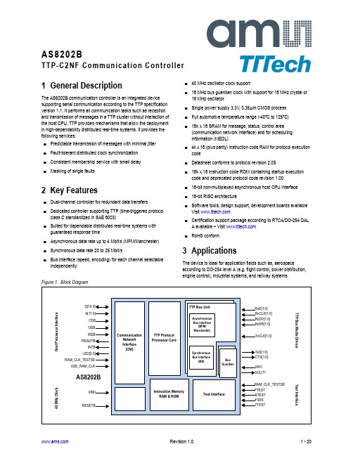
AS8202BTTP-C2NF Communication Controller1 General DescriptionThe AS8202B communication controller is an integrated device supporting serial communication according to the TTP specification version 1.1. It performs all communication tasks such as reception and transmission of messages in a TTP cluster without interaction of the host CPU. TTP provides mechanisms that allow the deployment in high-dependability distributed real-time systems. It provides the following services:⏹ Predictable transmission of messages with minimal jitter⏹ Fault-tolerant distributed clock synchronization⏹ Consistent membership service with small delay⏹ Masking of single faults2 Key Features⏹ Dual-channel controller for redundant data transfers⏹ Dedicated controller supporting TTP (time-triggered protocolclass C standardized in SAE 6003)⏹ Suited for dependable distributed real-time systems withguaranteed response time⏹ Asynchronous data rate up to 4 Mbit/s (MFM/Manchester)⏹ Synchronous data rate 20 to 25 Mbit/s⏹ Bus interface (speed, encoding) for each channel selectableindependently⏹ 40 MHz oscillator clock support⏹ 16 MHz bus guardian clock with support for 16 MHz crystal or16 MHz oscillator⏹ Single power supply 3.3V, 0.35µm CMOS process⏹ Full automotive temperature range (-40ºC to 125ºC)⏹ 16k x 16 SRAM for message, status, control area(communication network interface) and for schedulinginformation (MEDL)⏹ 4k x 16 (plus parity) instruction code RAM for protocol executioncode⏹ Datasheet conforms to protocol revision 2.05⏹ 16k x 16 instruction code ROM containing startup executioncode and deprecated protocol code revision 1.00⏹ 16-bit non-multiplexed asynchronous host CPU interface⏹ 16-bit RISC architecture⏹ Software tools, design support, development boards availableVisit ⏹ Certification support package according to RTCA/DO-254 DALA available – Visit ⏹ RoHS conform3 ApplicationsThe device is ideal for application fields such as, aerospace according to DO-254 level A (e.g. flight control, power distribution, engine control), industrial systems, and railway systems.Contents1 General Description (1)2 Key Features (1)3 Applications (1)4 Pin Assignments (3)4.1 Pin Descriptions (3)5 Absolute Maximum Ratings (6)6 Electrical Characteristics (7)7 Detailed Description (9)7.1 Host CPU Interface (9)7.1.1 Synchronous READYB Generation (12)7.2 Reset and Oscillator (13)7.2.1 External Reset Signal (13)7.2.2 Integrated Power-On Reset (13)7.2.3 Oscillator Circuitry (13)7.2.4 Built-in Characteristics (14)7.3 TTP Bus Interface (14)7.4 TTP Asynchronous Bus Interface (15)7.5 TTP Synchronous Bus Interface (15)7.6 Test Interface (16)7.7 LED Signals (16)8 Package Drawings and Markings (17)9 Ordering Information (19)4 Pin Assignments4.1 Pin DescriptionsTable 1. Pin DescriptionsPin Name Pin Number Dir DescriptionVDD4, 12, 29, 49, 59, 74Power pin Positive Power SupplyVSS13, 30, 41, 50, 60,75, 80Negative Power SupplyVDDBG70Positive Power Supply for Bus Guardian (connect to VDD) VSSBG73Negative Power Supply for Bus Guardian (connect to VSS)RAM_CLK_TESTSE21TTL Input with internal weak pull-downRAM_CLK when STEST=0 and USE_RAM_CLK=1, else Test Input, connect to VSS if not usedSTEST 22Test Input, connect to VSSFTEST 24Test Input, connect to VSSFIDIS 25Test Input, connect to VSSTTEST 61TTL Input with internal weak pull-upTest Input, connect to VDDUSE_RAM_CLK34TTL Input with internal weak pull-downRAM_CLK Pin Enable, connect to VSS if not usedXIN02Analog CMOS pinMain Clock: 40MHz external clock input CTEST 3Test input, to be unconnectedOSCMODE 23TTL Input with internal weak pull-downConnect to VDD 1XIN172Analog CMOS pinBus Guardian Clock: Analog CMOS Oscillator Input, use as input when providing external clockXOUT171Bus Guardian Clock: Analog CMOS Oscillator Output, leave open when providing external clockRESETB 26TTL Input with internal weak pull-up Main Reset Input, active lowTxD05TTL output with internal weak pull-up at tristate TTP Bus Channel 0: Transmit DataCTS06TTL output with internal weak pull-down at tristate TTP Bus Channel 0: Transmit EnableRxD011TTL Input with internal weak pull-upTTP Bus Channel 0: Receive DataTxCLK07TTL Input with internal weak pull-down TTP Bus Channel 0: Transmit Clock (MII mode)RxER08TTL Input with internal weak pull-up TTP Bus Channel 0: Receive Error (MII mode)RxCLK09TTL Input with internal weak pull-down TTP Bus Channel 0: Receive Clock (MII mode)RxDV010TTL Input with internal weak pull-up TTP Bus Channel 0: Receive Data Valid (MII mode)TxD114TTL output with internal weak pull-up at tristate TTP Bus Channel 1: Transmit DataCTS115TTL output with internal weak pull-down at tristate TTP Bus Channel 1: Transmit EnableRxD120TTL Input with internal weak pull-upTTP Bus Channel 1: Receive DataTxCLK116TTL Input with internal weak pull-down TTP Bus Channel 1: Transmit Clock (MII mode)RXER117TTL Input with internal weak pull-up TTP Bus Channel 1: Receive Error (MII mode)RXCLK118TTL Input with internal weak pull-down TTP Bus Channel 1: Receive Clock (MII mode)RxDV119TTL Input with internal weak pull-upTTP Bus Channel 1: Receive Data Valid (MII mode)Table 1. Pin DescriptionsPin Name Pin NumberDirDescriptionA[11:0]48-42, 39-35TTL InputHost Interface (CNI) Address Bus2D[15:0]69-62, 58-51TTL input/output with tristate Host Interface (CNI) Data Bus, tristateCEB 76TTL Input with internal weak pull-upHost Interface (CNI) chip enable, active lowOEB 77Host interface (CNI) output enable, active lowWEB 78Host interface (CNI) write enable, active lowREADYB 79TTL output with internal weak pull-up at tristateHost interface (CNI) transfer finish signal, active low, opendrain3INTB 28Host interface (CNI) time signal (interrupt), active low, open drain LED[2:0]33-31TTL output with internal weak pull-down at tristateConfigurable generic output portNC1, 27, 40Not connected, leave open1.This pin selects a clock multiplier of 1. This is the only supported operation mode.2.The device is addressed at 16-bit data word boundaries. If the device is connected to a CPU with a byte-granular address bus, remem-ber that A[11:0] of the AS8202B device has to be connected to A[12:1] of the CPU (considering a little endian CPU address bus)3.At de-assertion READYB is driven to the inactive value (high) for a configurable time.Table 1. Pin DescriptionsPin Name Pin Number Dir DescriptionDatasheet - A b s o lu t e M a x im u m R a ti n gs5 Absolute Maximum RatingsStresses beyond those listed in Table 2 may cause permanent damage to the device. These are stress ratings only. Functional operation of the device at these or any other conditions beyond those indicated in Electrical Characteristics on page 7 is not implied. Exposure to absolute maximum rating conditions for extended periods may affect device reliability.Table 2. Absolute Maximum RatingsSymbol Parameter Min Max Unit NotesElectrical ParametersV DD DC Supply voltage-0.3 5.0VV IN Input voltage-0.3V DD+0.3V any pinI IN Input current-100100mA any pin, T AMB=25ºC Electrostatic DischargeESD Electrostatic discharge1000V HBM: 1KV Mil.std.883, Method 3015.7 Temperature Ranges and Storage ConditionsT STRG Storage temperature-55+150ºCT BODY Package body temperature260ºC The reflow peak soldering temperature (body temperature) specified is in accordance with IPC/JEDEC J-STD-020 “Moisture/Reflow Sensitivity Classification for Non-HermeticSolid State Surface Mount Devices”. The lead finish for Pb-free leaded packages ismatte tin (100% Sn).H Humidity non-condensing585%MSL Moisture sensitivity level3Represents a maximum floor life time of 168h6 Electrical CharacteristicsT AMB= -40 to +125 ºC, V DD = 3V to +3.6V, V SS = 0V unless otherwise specified.Table 3. Electrical CharacteristicsSymbol Parameter Conditions Min Typ Max Unit Operating ConditionsI DDs Static Supply CurrentAll inputs tied to V DD/V SS,clocks stopped, exclusive of I/Odrive requirements, V DD=3.6V5900µAI DD Operating Supply Current(see note 1)VDD=3.3V,exclusive of I/O drive requirements100mACLK1Clock Period of Bus Guardian Clock(see note 1)62.5nsTTL Input Pins and TTL Bidirectional Pins in Input/Tristate ModelV IL Input Low Voltage0.8V V IH Input High Voltage 2.0VI INleak Input Leakage Current Pins without pad resistors,V DD=3.6V-11µAI IL Input Low Current Pins with pull-downresistors, V DD=3.0VV IN=0.4V4.9(see note 2)µAV IN=0.8V8.8(see note 2)Pins with pull-upresistorsV DD=3.6VV IN=0V-15-75I IH Input High Current Pins with pull-downresistorsV DD=3.6VV IN=3.6V1575µA Pins with pull-upresistors, V DD=3.0VV IN=2.0V-10.7(see note 2)V IN=2.5V-6(see note 2)C IN Input Capacitance4.5(see note2)pFRxD Pint ASYM_Rxt(V IN=0.5*V DD)Asymmetric Receiver Delay RxDT=125ºC, V DD=3.0V,C LOAD=35pF RxD[1,0]-2(see note 3)2(see note 3)nsCMOS Inputs (XIN), drive from external clock generatorDrive at XINC XIN Input Capacitance 1.9 2.5pFI XIN Input Current±1(see note 3)µA V IL_XIN Input Low Voltage00.3* V DD V V IH_XIN Input High Voltage0.7* V DD V DD V Outputs and TTL Bi-directional Pins in Output ModeI OL Output Low Current V DD=3.0V, Vo = 0.4V-4mAI OH Output High Current V DD=3.0V, Vo = 2.5V4mANotes:1. Typical values: CLK0=40 MHz (duty cycle 45-55%), CLK1=16 MHz.2. Implicitly tested.3. Guaranteed by design; not tested during production.I OZOutput Tristate CurrentV DD =3.6V±10(see note 3)µAt RISEt(V OUT =0.1*V DD )tot(V OUT =0.9*V DD )Transition Time – RiseT = 125 ºC, V DD =3.0V, C LOAD =35pFCTS[1,0], LED[2:0], INTB 8.1(see note 2)nsD[15:0], READYB 8.9(see note 2)t FALLt(V OUT =0.9*V DD )tot(V OUT =0.1*V DD )Transition Time – FallT = 125 ºC, V DD =3.0V, C LOAD =35pFCTS[1,0], LED[2:0], INTB 6(see note 2)nsD[15:0], READYB7(see note 2)TxD Pins t RISEt(V OUT =0.3*V DD )tot(V OUT =0.7*V DD )Transition Time – Rise TxDT = 125 ºC, V DD =3.0V, C LOAD =35pF TxD[1,0]4.5(see note 3)nst FALLt(V OUT =0.7*V DD )tot(V OUT =0.3*V DD )Transition Time – Fall TxD T = 125 ºC, V DD =3.0V, C LOAD =35pF TxD[1,0]3(see note 3)nst ASYM_Rxt(V OUT =0.5*V DD ) Asymmetric Driver Delay TxD T = 125 ºC, V DD =3.0V, C LOAD =35pFTxD[1,0]-3(see note 3)3(see note 3)nsTable 3. Electrical CharacteristicsSymbol Parameter Conditions Min Typ Max Unit7 Detailed DescriptionThe AS8202B is the first TTP controller to support both MFM and Manchester coding. Manchester coding is important for DC-free data transmission, which allows the use of transformers in the data stream. The AS8202B is pin-compatible with its predecessor, the AS8202. The AS8202B provides support for fault-tolerant, high-speed bus systems in a single device. The communication controller is qualified for the full temperature range required for automotive applications and is certifiable according to RTCA standards. It offers superior reliability and supports data transfer rates of 25 Mbit/s with MII and up to 4 Mbit/s with MFM/Manchester.The CNI (communication network interface) forms a temporal firewall. It de-couples the controller network from the host subsystem by use of a dual ported RAM (CNI). This prevents the propagation of control errors. The interface to the host CPU is implemented as a 16-bit wide non-multiplexed asynchronous bus interface.The TTP follows a conflict-free media access strategy called time division multiple access (TDMA). This means, TTP deploys a time slot technique based on a global time that is permanently synchronized. Each node is assigned a time slot in which it is allowed to perform transmit operation. The sequence of time slots is called TDMA round, a set of TDMA rounds forms a cluster cycle. The operation of the network is repeated after one cluster cycle. The sequence of interactions forming the cluster cycle is defined in a static time schedule, called message descriptor list (MEDL). The definition of the MEDL in conjunction with the global time determines the response time for a service request.The membership of all nodes in the network is evaluated by the communications controller. This information is presented to all correct cluster members in a consistent fashion. During operation, the status of all other nodes is propagated within one TDMA round. Please read more about TTP and request the TTP specification at .7.1 Host CPU InterfaceThe host CPU interface, also referred to as CNI (Communication Network Interface), connects the application circuitry to the AS8202B TTP controller. All related signal pins provide an asynchronous read/write access to a dual ported RAM located in the AS8202B. There are no setup/ hold constraints referring to the microtick (main clock “CLK0”).All accesses have to be executed on a granularity of 16-bit (2 byte), the device does not support byte-wide accesses. The pin A0 (LSB) of the device differentiates even and odd 16-bit word addresses and is typically connected to A1 of a little-endian host CPU. The A0 of host CPU is not connected to the device, and the application/driver on the host CPU should force all accesses to be 16-bit. For efficiency reasons, the host CPU application/driver may access some memory locations of the AS8202B using wider accesses (e.g. 32-bit), and the bus interface of the host CPU will automatically split the access into two consecutive 16-bit wide accesses to the TTP controller. Note that particularly in such a setup all timing parameters of the host CPU interface must be met, especially the inactivity timeouts described as symbols 16–19.The host interface features an interrupt or time signal INTB to notify the application circuitry of programmed and protocol-specific, synchronous and asynchronous events.The host CPU interface allows access to the internal instruction code memory. This is required for proper loading of the protocol execution code into the internal instruction code RAM, for extensive testing of the instruction code RAM and for verifying the instruction code ROM contents. INTB is an open-drain output, i.e. the output is only driven to '0' and is weak-pull-up at any other time, so external pull-up resistors or transistors may be necessary depending on the application.READYB is also an open-drain output, but with a possibility to be driven to ‘1’ for a defined time (selectable by register) before weak-pull-up at any other time.The LED port is software-configurable to automatically show some protocol-related states and events, see below for the LED port configuration. Table 4. Host Interface PortsPin Name Mode Width CommentA[11:0]in12CNI address bus, 12-bit (A0 is LSB)D[15:0]inout (tri)16CNI data bus, 16-bit (D0 is LSB)CEB in1CNI chip enable, active lowWEB in1CNI write enable, active lowOEB In1CNI output enable, active lowREADYB out (open drain)1CNI ready, active lowINTB out (open drain)1CNI interrupt, time signal, active low RAM_CLK_TESTSE in1HOST clockUSE_RAM_CLK in1HOST clock pin enableAsynchronous READYB permits the shortest possible bus cycle but eventually requires signal synchronization in the application. Connect USE_RAM_CLK to VSS to enable this mode of operation.Synchronous READYB uses an external clock (usually the host processor’s bus clock) for synchronization of the signal, eliminating external synchronization logic. Connect USE_RAM_CLK to VDD and RAM_CLK_TESTSE to the host processor's bus clock to enable this mode of operation.Note:Due to possible metastability occurrence, it is not recommended to be used in safety critical systems.Table 5. Asynchronous DPRAM InterfaceSymbol Parameter Conditions Min Typ Max Units Tc Controller Cycle Time25ns1aInput Valid to CEB, WEB (Setup Time)A[11:0]5ns2a D[15:0]1bCEB, WEB to Input Invalid (Hold Time)A[11:0]3ns2b D[15:0]43Input Rising to CEB, WEB Falling CEB, WEB, OEB5(see note 1)ns4CEB, WEB Rising to Input Falling CEB, WEB, OEB5(see note 1,2)ns5Write Access Time (CEB, WEB toREADYB)Min = 1 Tc, Max = 4 Tc25100ns6CEB, WEB de-asserted to READYBde-asserted9.4ns 7a Input Valid to CEB, OEB (Setup Time)A[11:0]5ns 7b CEB, OEB to Input Invalid (Hold Time)A[11:0]2ns8Input Rising to CEB, OEB Falling CEB, WEB, OEB5(see note 1)ns9CEB, OEB Rising to Input Falling CEB, WEB, OEB5(see note 1)ns10Read Access Time (CEB, OEB toREADYB)Min = 1.5 Tc, Max = 8 Tc37.5200ns 11a CEB, OEB asserted to signal asserted D[15:0] 4.08.4ns11b CEB, OEB de-asserted to signal de-asserted D[15:0] 3.88ns11c READYB8.812READYB, D skew±2ns13RAM_CLK_TESTSE Rising toREADYB Falling USE_RAM_CLK=1 3.713.5ns14RAM_CLK_TESTSE Rising toREADYB Rising USE_RAM_CLK=139.7ns15RAM_CLK_TESTSE Rising toREADYB Deactivated 1->Z USE_RAM_CLK=1Readydelay=00 3.612.9nsReadydelay=01 4.515.4Readydelay=10 5.418.8Readydelay=11 6.422.216Read to Read Access Inactivity Time(CEB, OEB low to CEB, OEB low)Min = 1.5 Tc37.5(see note 1)nsNotes:1. Prior to starting a read or write access, CEB, WEB and OEB have to be stable for at least 5 ns (see symbol 3, 4, 8, 9). In addition the designer has to consider the minimum inactivity time according to symbols 16, 17, 18, 19. For more information on the inactivity times (see Figure 3).2. To allow proper internal initialization, after finishing any write access (CEB or WEB is high) to the internal CONTROLLER_ON register, CEB OEB and WEB have to be stable high within 200 ns (min = 8 Tc).3. All values not tested during production, guaranteed by design.Figure 3. Read/Write Access Inactivity Time17Read to Write Access Inactivity Time (CEB, OEB low to CEB, WEB low)5(see note 1)ns 18Write to Write Access Inactivity Time (CEB, WEB low to CEB, WEB low)5(see note 1,2)ns 19Write to Read Access Inactivity Time (CEB, WEB low to CEB, OEB low)5(see note 1,2)nsTable 5. Asynchronous DPRAM InterfaceSymbol ParameterConditionsMin Typ Max UnitsFigure 5. Write Access Timing (WEB Controlled)Figure 6. Read Access Timing (CEB Controlled)Figure 7. Read Access Timing (OEB Controlled)7.1.1 Synchronous READYB GenerationSynchronous READYB is aligned to host clock (with pulse duration of one host clock cycle) to fulfill the required host timing constraints for input setup and input hold time to/after host clock rising edge.Note:Connect USE_RAM_CLK to VDD and RAM_CLK_TESTSE to the host processor's bus clock to enable this mode of operation. Due topossible metastability occurrence, it is not recommended to be used in safety critical systems.7.2 Reset and Oscillator7.2.1 External Reset SignalTo issue a reset of the chip the RESETB port has to be driven low for at least 1µs. Pulses under 50ns duration are discarded. At power-up the reset must overlap the build-up time of the power supply. This reset may only be used if a proper power-on reset can be ensured (refer to Section 7.2.2 Integrated Power-On Reset).7.2.2 Integrated Power-On ResetThe device has an internal Power-On-Reset generator. When supply voltage ramps up, the internal reset signal is kept active (low) for 33µs typical.Note:In case of non-compliance keep the external reset (RESETB) active for min. 5 ms after supply voltage is valid and main clock is stable.7.2.3 Oscillator CircuitryThe main clock requires an external oscillator. The bus guardian requires an external oscillator or an external quartz.Figure 9. Main Clock SetupXIN0 of the main clock shall be supplied by a 40MHz clock provided by an oscillator IC.Table 6. Pin ModePin Name Mode CommentXIN1analog Bus guardian oscillator input (external clock input)RESETBinExternal resetTable 7. ParametersSymbol Parameter Min Typ Max Unit dV/dt supply voltage slope551--V/ms tporespower on reset active time after VDD > 1,0V253349µsExternal oscillator 40MHz square waveX I N OFigure 10. Bus Guardian Clock SetupThe bus guardian clock (XIN1/XOUT1) supports driving a quartz crystal oscillation, as well as a clock input by an external oscillator.7.2.4 Built-in Characteristics7.3 TTP Bus InterfaceThe AS8202B contains two TTP bus units, one for each TTP channel, building the TTP bus interface. Each TTP bus channel contains atransmitter and a receiver and can be configured to be either in the asynchronous or synchronous mode of operation. Note that the two channels (channel 0 and channel 1) can be configured independently for either of these modes.The drivers of the TxD and CTS pins are actively driven only during a transmission window, all the other time the drivers are switched off and the weak pull resistors are active. External pull resistors must be used to define the signal levels during idle phases.Note:The transmission window may be different for each channel.Table 8. CharacteristicsSymbol Pin Parameter MinTypMax Unit Note Tosc_startup1XIN1/XOUT1Oscillator startup time (Bus Guardian clock)20msFrequency: 16MHzTable 9. Bus Interface ConnectionsPin Name Tx inactive TxD[0]weak pull-up CTS[0]weak pull-down TxD[1]weak pull-up CTS[1]weak pull-down7.4 TTP Asynchronous Bus InterfaceWhen in asynchronous mode of operation the channel's bus unit uses a self-clocking transmission encoding which can be either MFM orManchester at a maximum data rate of 4 Mbit/s on a shared media (physical bus). The pins can either be connected to drivers using recessive/dominant states on the wire as well as drivers using active push/pull functionality.The RxD signal uses '1' as the inactivity level. In the so-called RS485 compatible mode longer periods of '0' are treated as inactivity. If the RS485 compatible mode is not used, the application must care to drive RxD to '1' during inactivity on the bus.7.5 TTP Synchronous Bus InterfaceWhen in synchronous mode of operation, the bus unit uses a synchronous transfer method to transfer data at a rate between 20 and 25 Mbit/s. The interface is designed to run at 25 Mbit/s and to be fully compatible with the commercial 100 Mbit/s Ethernet MII (Media Independent Interface) according to IEEE standard 802.3 (Ethernet CSMA/CD).Connecting the synchronous TTP bus unit to a 100 Mbit/s Ethernet PHY is done by connecting TxD, CTS, TxCLK, RXER, RXCLK, RxDV and RxD of any channel to TxD0TxD0, TxEN, TxCLK, RXER, RXCLK, RxDV and RxD0 of the PHY's MII. The pins TxD1, TxD2 and TxD3 of the PHY's MII should be linked to VSS. The signals RxD1, RxD2, RxD3, COL and CRS as well as the MMII (Management Interface) should be left open or can be used for diagnostic purposes by the application.Note that the frames sent by the AS8202B are not Ethernet compatible and that an Ethernet Hub (not a Switch) can be used as a 'star coupler' for proper operation. Also note that the Ethernet PHY must be configured for Full Duplex operation (even though the Hub does not support full duplex), because TTP has its own collision management that should not interfere with the PHY's Half-Duplex collision management. In general, the PHY must not be configured for automatic configuration ('Auto negotiation') but be hard-configured for 100 Mbit/s, Full Duplex operation.Note:To run the interface at a rate other than 25 Mbit/s other transceiver PHY components have to be used.Table 10. Asynchronous Bus Interface ConnectionsPin Name Mode Connect to PHYNoteTxD[0]out TxD Transmit data channel 0CTS[0]out CTSTransmit enable channel 0TxCLK[0]in No function (do not connect)RXER[0]in No function (do not connect)RXCLK[0]in No function (do not connect)RxDV[0]in No function (do not connect)RxD[0]in RxD Receive data channel 0TxD[1]out TxD Transmit data channel 1CTS[1]out CTS Transmit enable channel 1TxCLK[1]in No function (do not connect)RXER[1]in No function (do not connect)RXCLK[1]in No function (do not connect)RxDV[1]in No function (do not connect)RxD[1]inRxD Receive data channel 1Table 11. Synchronous Bus Interface ConnectionsPin Name Mode Connect to PHY NoteTxD[0]out TxD0TxD0Transmit data channel 0CTS[0]out TxEN Transmit enable channel 0TxCLK[0]in TxCLK Transmit clock channel 0RXER[0]in RXER Receive error channel 0RXCLK[0]in RXCLK Receive clock channel 0RxDV[0]inRxDVReceive data valid channel 07.6 Test InterfaceThe Test Interface supports the manufacturing test and characterization of the chip. In the application environment test pins have to be connected as following:⏹ STEST, FTEST, FIDIS: connect to VSS ⏹ TTEST: connect to VDD7.7 LED SignalsThe LED port consists of three pins. Via the MEDL each of these pins can be independently configured for any of the three modes of operation. At Power-Up and after Reset the LED port is inactive and only weak pull-down resistors are connected. After the controller is switched on by the host and when it is processing its initialization, the LED port is initialized to the selected mode of operation.Each LED pin can be configured to be either a push/pull driver (drives both LOW and HIGH) or to be only an open-drain output (drives only LOW).RxD[0]in RxD0Receive data channel 0TxD[1]out TxD0Transmit data channel 1CTS[1]out TxEN Transmit enable channel 1TxCLK[1]in TxCLK Transmit clock channel 1RXER[1]in RXER Receive error channel 1RXCLK[1]in RXCLK Receive clock channel 1RxDV[1]in RxDV Receive data valid channel 1RxD[1]inRxD0Receive data channel 1Caution:Any other connection of these pins may cause permanent damage to the device and to additional devices of the application.Table 12. LED SignalsPin Name Protocol Mode Timing Mode Bus Guardian ModeLED2RPV 1orProtocol activity 71.RPV is Remote Pin Voting. RPV is a network-wide agreed signal used typically for agreed power-up or power-down of the application's external drivers.Time Overflow 22.Time Overflow is active for one clock cycle at the event of an overflow of the internal 16-bit time counter. Time Tick is active for one clock cycle when the internal time is counted up. Time Overflow and Time Tick can be used to externally clone the internal time control unit (TCU). With this information the application can precisely sample and trigger events, for example.Action Time 33.Action Time signals the start of a bus access cycle.LED1Sync Valid44.The controller sets this output when cluster synchronization is achieved (after integration from the LISTEN state, after acknowledge in the COLDSTART state).Time Tick 2BDE1 55.BDE0 and BDE1 show the Bus Guardian's activity, '1' signals an activated transmitter gate on the respective channel.LED0Protocol activity 6 or RPV76.Protocol activity is typically connected to an optical LED. The flashing frequency and rhythm give a simple view to the internal TTP pro-tocol state.7.LED2's RPV mode and LED0's Protocol activity mode can be swapped with a MEDL parameter.Microtick88.Microtick is the internal main clock signal.BDE05Table 11. Synchronous Bus Interface ConnectionsPin Name Mode Connect to PHYNote。
ISPGAL22V10中文资料
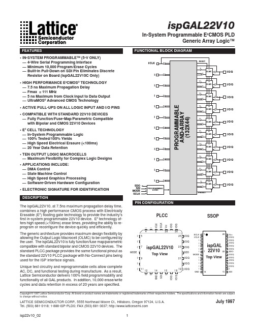
I I GND SDI I I/O/Q I/O/Q
FUNCTIONAL BLOCK DIAGRAM
I/CLK
I
I
I
I
I
I
I
I
I
SDO SDI MODE SCLK
I
PROGRAMMING LOGIC
PIN CONFIGURATION
PROGRAMMABLE AND-ARRAY (132X44)
RESET 8 OLMC
Industrial Grade Specifications
Tpd (ns) 15
Tsu (ns) 10
Tco (ns) 8
Icc (mA)
Ordering #
165 ispGAL22V10C-15LJI
ispGAL22V10C-15LKI
Package 28-Lead PLCC 28-Lead SSOP 28-Lead PLCC 28-Lead PLCC 28-Lead SSOP 28-Lead PLCC 28-Lead PLCC 28-Lead SSOP 28-Lead PLCC
4
2
28
26
I5
2 5 I/O/Q
SCLK I/CLK
1
28 Vcc I/O/Q
I
I7 MODE
I9
ispGAL22V10 Top View
I/O/Q
I
I/O/Q
I
I/O/Q
2 3 I/O/Q
I
ispGAL I/O/Q
SDO
22V10 I
I7
I/O/Q 22 SDO
MODE
I/O/Q
2 1 I/O/Q
July 1997
德国光产品X4 BAR 10 20程序员注意事项说明书

*******************************P r o g r a m m i n g N o t e sThis guide will serve as an outline for the various DMX modes for the X4 BAR 10 and X4 BAR 20 with a focus on Normal Mode to assist in understanding how to program the fixtures when set to this DMX Mode.Normal Mode in the X4 BAR fixture implements a unique layer effect system that allows for an extremely wide array of effects whilst using a minimum of DMX Channels.You can choose between 7 DMX modes each designed for different applications and preferences:•Normal Mode (BAR 20 - 34 Channels / BAR 10 - 33 Channels): Most common mode with all basic functions with layered effect features •Compressed Mode (BAR 20 - 19 Channels / BAR 10 - 19 ): Limited channel mode.Channels are sorted to match the impression X4 normal mode.•High Resolution Mode (BAR 20 - 35 Channels / BAR 10 - 34 Channels): Same as the Normal Mode but with 16bit Master Intensity dimming •Single Pixel Mode (BAR 20 - 88 Channels / BAR 10 - 48 Channels): Individual control of the RGBW values for each pixel (i.e. for pixel mapping)•Single Pixel High Resolution Mode (BAR 20 - 89 Channels / BAR 10 -49 Channels):Same as the Single Pixel Mode but with 16bit Master Intensity dimming •Dual Pixel Mode (BAR 20 - 48 Channels / BAR 10 – 28 Channels): Same as the Single Pixel Mode but with 2 pixel combined as one to reduce the channel count.•Dual Pixel High Resolution Mode (BAR 20 - 49 Channels / BAR 10 - 29 Channels):Same as the Dual Pixel Mode but with 16bit Master Intensity dimmingThe example that will be shared in these notes will apply to both the X4 BAR 10 and the X4 BAR 201 Guide to the Set Layers•There are 3 Set Layers for the fixture.•Set 1 and Set 2 have 8 channels each attributed to their functionality o Set 1 or 2 Color Wheelo Set 1 or 2 Redo Set 1 or 2 Greeno Set 1 or 2 Blueo Set 1 or 2 Whiteo Set 1 or 2 Intensityo Set 1 or 2 Pattern Selecto Set 1 or 2 Pattern Movement•Set 3 has 6 channels attributed to its functionalityo Set 3 Color Wheelo Set 3 Redo Set 3 Greeno Set 3 Blueo Set 3 Whiteo Set 3 Intensity•Set Layer 1 has highest priority over Set Layers 2 & 3 with Set Layer 2 having priority over Set Layer 3•Pixel Select 1 – 8, Pixel Select 9 – 16, Pixel Select 17 – 20 are for custom patterns and apply only to Set Layer 1 when Pattern Select is at value 255•Shutter and Master Intensity take precedent over all 3 Set Layers•Crossfade allows for the fade instead of snap in Set Layer Movement Effects•Star Effect randomly strobes all pixels in all active Set Layers2 An Example to Demonstrate the Set Layers Functions•This demonstration uses the X4 BAR 20•Make sure the fixture is patched to a Normal Mode library and the fixture is set to Normal Modeo Fixture libraries from different console manufacturers will vary on how the library is patched in regards to which channel is patched towhich attribute. Some Console libraries require that the fixture be amulti part fixture. Please check with the Console manufacture orConsole Fixture library editor to verify the correct channel patchand layout.o All channel numbers noted are in parentheses and applied as in the DMX chart. All values are in DMX 8 bito The demonstration will use Red for Set Layer 1, Green for SetLayer 2 and Blue for Set Layer 31. Select the fixture2. Choose the Shutter Channel(11) and set to value 2553. Choose the Master Intensity Channel(12) and set to value 2554. Choose Set 1 Red(6) and set to value 2555. Choose Set 1 Intensity(10) and set to value 2556. All the pixels of the of the fixture should now be Red7. Choose Set Pattern 1 Select(28) and set to value 8a. If the value of Set Pattern 1 stay at value 0, then it will takeprecedence and layers 2 and 3 will not be seen.8. Pixels 1-5 should be Red and 6 – 20 should be blacked out as shownbelow:9. Choose Set 2 Green(16) and set to 25510. Choose Set 2 Intensity(19) and set to 25511. Pixels 1-5 should be Red and 6 – 20 should now be Green as shownbelow:12. Choose Set Pattern 2 Select(30) and set to value 13a. If the value of Set Pattern 1 stay at value 0, then it will takeprecedence and layers 2 and 3 will not be seen.13. Pixels 1-5 should be Red and 6 – 10 should now be Green with 11 – 20being blacked out as shown below:a. The value set for Set Pattern 2 Select has activated pixels 1 -10 ingreen, but Set Pattern 1 has precedence over pixels 1 – 5 so theyare still Red14. Choose Set 3 Blue(23) and set to 25515. Choose Set 3 Intensity(25) and set to 25516. Pixels 1-5 should be Red and 6 – 10 should now be Green with 11 – 20 inBlue as shown below:a. Select Set 3 with Blue will now always be in the background17. Choose Set 1 Pattern Movement(29) and set to 170a. The Red pixels at 1 – 5 will now chase from left to right, leavingGreen in pixels 1 – 10, and Blue in Pixels 11 – 2018. Choose Set 2 Pattern Movement(31) and set to 190a. The Green pixels at 1 – 10 will now chase from right to left, as the 5Red pixels continue to chase left to right and blue remains in thebackground19. Choose Crossfade(26) to affect the fading from color to color within theSet Layers.20. Choose Star Effect(27) to create a random strobing of each individualpixel.3 Normal Mode (norm) 34 DMX channels:Channel Function Time and Value DMX1 Tilt - High Tilt coarse 0° - 210°0..2552 Tilt - Low Tilt fine 0..2553 Zoom Wide (flood) - narrow (spot) 50° - 7°0..2554 CTO No CTO 0..7Continuous color temperature correction Applicable 8..255for ALL colors5 Set 1 Color(fixed) Colors adjustable via RGB 0..7 Color 01 - Red 1)8..15 Color 02 - Amber 1)16..23 Color 03 - Warm Yellow 1)24..31 Color 04 - Yellow 1)32..39 Color 05 - Green 1)40..47 Color 06 - Turquoise 1)48..55 Color 07 - Cyan 1)56..63 Color 08 - Blue 1)64..71 Color 09 - Lavender 1)72..79 Color 10 - Mauve 1)80..87 Color 11 - Magenta 1)88..95 Color 12 - Pink 1)96..103 White - CTO 3200K 104..111 White 5600K 112..119 White - CTB 7200K 120..127 Rainbow Effect Stop 2)128 Rainbow Effect 3)slow - fast 129..223 Random colors slow - fast 224..2556 Set 1 Red Color mixing system - Red 0 - 100% 0..2557 Set 1 Green Color mixing system - Green 0 - 100% 0..2558 Set 1 Blue Color mixing system - Blue 0 - 100% 0..2559 Set 1 White Color mixing system - White 0 - 100% 0..25510 Set 1 Intensity Intensity 0 - 100% 0..25511 Shutter Shutter closed 0..15Shutter pulse random slow – fast 16..47Fade on, snap off (random patterns) slow – fast 48..79Snap on, fade off (random patterns) slow – fast 80..111Fade on, fade off (random patterns) slow – fast 112..143Strobe random 5s - 0.1s 144..199Strobe effect slow - fast 1 Hz - 10 Hz 200..239Shutter open 240..25512 Master Intensity Intensity 0 - 100% 0..25513 Special 5)See special features below 5)- -14 Set 2 Color 4)Values see Channel 5 - -15 Set 2 Red 4)Color mixing system - Red 0 - 100% 0..25516 Set 2 Green 4)Color mixing system - Green 0 - 100% 0..25517 Set 2 Blue 4)Color mixing system - Blue 0 - 100% 0..25518 Set 2 White 4)Color mixing system - White 0 - 100% 0..25519 Set 2 Intensity 4)Intensity 0 - 100% 0..25520 Set 3 Color 4)Values see Channel 5 - -21 Set 3 Red 4)Color mixing system - Red 0 - 100% 0..25522 Set 3 Green 4)Color mixing system - Green 0 - 100% 0..25523 Set 3 Blue 4)Color mixing system - Blue 0 - 100% 0..25524 Set 3 White 4)Color mixing system - White 0 - 100% 0..25525 Set 3 Intensity 4)Intensity 0 - 100% 0..25526 Crossfade 0..2 seconds transition time 0..25527 Star Effect Random internal shutter effect slow – fast 0..25528 Set 1 Pattern 0..255Select29 Set 1 Pattern 0..255Movement30 Set 2 Pattern 0..255Select31 Set 2 Pattern 0..255Movement32 Pixel Select 0..2551 - 833 Pixel Select 0..2559 - 1634 Pixel Select 0..25517 - 204 Special Channel Addendum5) Special Channel Function Overview:DMX valueActive Function Save toeepromRemarksfrom to03not in SPix/DPix mode no mirror no47not in SPix/DPix mode mirror color priority no811not in SPix/DPix mode mirror color mixing noThe following switch boxes only work if special channel has been enabled with DMX value zero (0) before: 128 131 3 seconds Tilt current off yes Only applicable from Tilt Firmware V.015 6) 132 135 3 seconds Tilt current on yes Only applicable from Tilt Firmware V.015 6) 136 139 3 seconds Tilt reset off yes Only applicable from Tilt Firmware V.015 6) 140 143 3 seconds Tilt reset on yes Only applicable from Tilt Firmware V.015 6) 144 147 3 seconds Display Flip off yes148 151 3 seconds Display Flip on yes152 155 3 seconds DMX Mode DPixH(HiRes)yesonly if shutter=48..49 and intensity=50..51(12800..13056 at high resolution)156 159 3 seconds DMX Mode SPixH(HiRes)yesonly if shutter=48..49 and intensity=50..51(12800..13056 at high resolution)160 163 3 seconds DMX Mode HighResolutionyesonly if shutter=48..49 and intensity =50..51(12800..13056 at high resolution)164 167 3 seconds DMX Mode Normal yes only if shutter=48..49 and intensity =50..51 (12800..13056 at high resolution)168 171 3 seconds DMX ModeCompressedyesonly if shutter=48..49 and intensity =50..51(12800..13056 at high resolution)172 175 3 seconds DMX Mode DPix yes 176 179 3 seconds DMX Mode SPix yes 180 183 3 seconds Dimmer Curve ESoft yes 184 187 3 seconds Dimmer Curve Soft yes 188 191 3 seconds Dimmer Curve Lin yes 192 195 3 seconds X4 Compatibility off yes 196 199 3 seconds X4 Compatibility on yes 200 203 3 seconds Silent-Mode off yes 204 207 3 seconds Silent-Mode on yes 208 211 3 seconds Position Feedback off yes 212 215 3 seconds Position Feedback on yes 216 219 3 seconds DMX hold off yes 220 223 3 seconds DMX hold on yes 224 227 3 seconds Tilt invers off yes 228 231 3 seconds Tilt invers on yes 232 235 3 seconds Pixel invers off yes 236 239 3 seconds Pixel invers on yes 240 243 3 seconds Zoom invers off yes 244 247 3 seconds Zoom invers on yes 248 251 3 seconds Fixture default yes 252 255 3 seconds Fixture reset no。
- 1、下载文档前请自行甄别文档内容的完整性,平台不提供额外的编辑、内容补充、找答案等附加服务。
- 2、"仅部分预览"的文档,不可在线预览部分如存在完整性等问题,可反馈申请退款(可完整预览的文档不适用该条件!)。
- 3、如文档侵犯您的权益,请联系客服反馈,我们会尽快为您处理(人工客服工作时间:9:00-18:30)。
19, Innovation First Road •Science Park •Hsin-Chu •Taiwan 300•R.O.C.SPHE8202VDesign GuideV1.0-Jul 29, 2010s u n p l u s f o r z i h u a nImportant Notice SUNPLUS TECHNOLOGY CO. reserves the right to change this documentation without prior notice. Information provided by SUNPLUS TECHNOLOGY CO. is believed to be accurate and reliable. However, SUNPLUS TECHNOLOGY CO. makes no warranty for any errors which may appear in this document. Contact SUNPLUS TECHNOLOGY CO. to obtain the latest version of device specifications before placing your order. No responsibility is assumed by SUNPLUS TECHNOLOGY CO. for any infringement of patent or other rights of third parties which may result from its use. In addition, SUNPLUS products are not authorized for use as critical components in life support systems or aviation systems, where a malfunction or failure of the product may reasonably be expected to result in significant injury to the user, without the express written approval of Sunplus.s un p l u s f o r z i hRevisionDate ByRemark Page Number(s)V1.02010/07/29Ingrid First 18s un p l u s f o r z i hPAGE SPHE8202V (1)Design Guide ......................................................................................................................................11 System Overview.............................................................................................................................31.1 System Block Diagram................................................................................................................31.2 System Feature...........................................................................................................................42 System Design Guideline................................................................................................................52.1 SDRAM.......................................................................................................................................52.2 SPI Flash (5)2.3 Video (6)2.4 Audio (7)2.5 RESET Circuit (7)2.6 USB2.0 (8)2.7 UART (9)2.8 Card Reader (9)2.9 SCART (10)2.10 Core Power (10)2.11 Servo (OPU & Motor Driver) (10)3 EMI Considerations (15)3.1 Crystal (15)3.2 Loader Control Signals (15)3.3 PCB Layout...............................................................................................................................16s u n p l u s f o r z i h1 System Overview 1.1 System Block DiagramSPHE8202V 支援DVD/CD servo 、TV encoder 、Audio ADC 2ch 、internal Audio DAC 5.1ch 、GAME 、USB 2.0、3in1Card reader 等等…,圖1-1為SPHE8202V 系統方塊圖。
Figure 1-1SPHE8202V System Block Diagrams u n p l us f o r z i h1.2 System Feature•SOC (RF integrated)•Support MPEG4•Support USB 2.0•Support 3in1 Card Reader (SD, MS, MS-pro, MMC)•SDRAM: Support 16 M / 64M bits, with 16 bits mode •ROM/FLASH: Support SPI flash •Support boot-strap mode •TV: 4 TV DAC output (full current output)•Audio: internal DAC 5.1ch output, support AC3, DTS and SPDIF OUT •MIC: Support internal ADC (2ch) function •Support IR / VFD interface •Support 8bits game pad •Support full color Native32 game •Support CD-Ripping s un p l u s f o r z i h2 System Design Guideline 2.1 SDRAM(1)SPHE8202V support 16-bit mode ,如圖2-1。
Figure 2-1SDRAM 16-bit mode(2)SPHE8202V system clock 最高可能會跑在155.25MHZ ,在clock 走線上要特別注意,SDRAM 盡量靠近8202V IC 。
(3)建議在SDRAM clock 上最好加RC (R 為33 ohm ,C 為10 pF)電路。
(4)新增一根CKE pin ,可以節省SDRAM 功耗損失以及在系統進入standby mode 時,這根pin 可以讓SDRAM 進入power down mode ,如此一來系統可以在standby mode 時節省功耗。
2.2 SPI Flash在SPI flash 部份建議電路如圖2-2,其中R1為10K ohm ,R2為0 ohm 。
另外建議在SPI_CS pin 上加pull high 電阻R3=10K ohm ,為避免有一些SPI flash 在上電的時候發生問題。
s u n p l us f o r z i hFigure 2-2SPI Flash Circuit2.3 Video(1)SPHE8202V 在Video 預設為全電流模式,由於8202V 只有支援SD output ,因此建議filter 相關參數如圖2-3。
另外COMP 輸出接的參考電容為10uF ,Rset 為1K ohm 。
建議將對地的75歐姆電阻擺放靠近SPHE8202V ,以期獲得較佳的video quality 。
同時,ESD 元件的正電壓建議接到3.3V 以及擺放於connector 及π型濾波線路中間靠近connector 處。
Figure 2-3SD DAC -buffer + filter + protector(2)SPHE8202V 的video power 由於是比較耗電的部分,因此務必從3,3V 分支,並且接上大電容,在SPHE8202V 端每一video power pin 前皆要有bypass 電容。
s u n p l u s fo r z i hFigure 2-4Video Power 2.4 AudioSPHE8202V audio 有5.1ch output ,前面2個channel 是DAC output ,後面4個channel 是數位的PWM output ,在OP 線路的部分不太一樣,詳細請參考線路圖的部分。
而8202V audio 相關的power 共有3pin ,有audio ADC 、DAC 跟PWM 的部分,建議PWM power 跟其他power 要分開。
在Audio ADC input 的部份支援2ch input ,這2個聲道架構是相同的,如果只有用到一個聲道的話另一根pin 可以拿來當GPIO 使用。
Figure 2-5Audio power2.5 RESET Circuit為了確保整個系統能正常工作,建議系統的reset circuit 能依照圖2-6來製作。