1SMA5917A中文资料
AD5791_cn 中文说明书

件执行一次有效的写操作为止。输出箝位特性可将输出置 于已定义的负载状态。
产品聚焦 1. 1 ppm精度。 2. 宽电源电压范围:最高达±16.5V。 3. 工作温度范围:−40°C至+125°C。 4. 低噪声频谱密度:7.5 nV/√Hz。 5. 低温度漂移:0.05ppm/°C。
Rev. 0
Information furnished by Analog Devices is believed to be accurate and reliable. However, no responsibility is assumed by Analog Devices for its use, nor for any infringements of patents or other rightsofthirdpartiesthatmayresultfromitsuse.Speci cationssubjecttochangewithoutnotice.No license is granted by implication or otherwise under any patent or patent rights of Analog Devices. Trademarks and registered trademarks are the property of their respective owners.
最小值
20 −1
−1.5 −1.5 −3 −4 −1 −1.5 −2.5
−3 −5 −9
−1.5 −2.5 −9
−6 −10 −20
−3 −3 −3
VREFN
A、B级1 典型值 最大值
±0.25 +1
±0.25 +1.5
SMA71资料
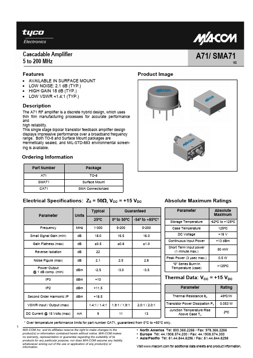
元器件交易网Cascadable Amplifier 5 to 200 MHzFeatures• • • • AVAILABLE IN SURFACE MOUNT LOW NOISE: 2.1 dB (TYP.) HIGH GAIN 18 dB (TYP.) LOW VSWR <1.4:1 (TYP.)A71/ SMA71V2Product ImageDescriptionThe A71 RF amplifier is a discrete hybrid design, which uses thin film manufacturing processes for accurate performance and high reliability. This single stage bipolar transistor feedback amplifier design displays impressive performance over a broadband frequency range. Both TO-8 and Surface Mount packages are Hermetically sealed, and MIL-STD-883 environmental screening is available.Ordering InformationPart NumberA71 SMA71 CA71PackageTO-8 Surface Mount SMA ConnectorizedElectrical Specifications: Z0 = 50Ω, VCC = +15 VDC ΩTypical ParameterFrequency Small Signal Gain (min) Gain Flatness (max) Reverse Isolation Noise Figure (max) Power Output @ 1 dB comp. (min) IP3 IP2 Second Order Harmonic IP VSWR Input / Output (max) DC Current @ 15 Volts (max) mAAbsolute Maximum RatingsParameterStorage Temperature Case Temperature DC Voltage Continuous Input Power Short Term Input power (1 minute max.)Guaranteed 0º to 50ºC5-200 16.5 ±0.8Units 25ºCMHz dB dB dB dB dBm dBm dBm dBm 1-300 18.0 ±0.5 22 2.1 -2.5 +10 +11.5 +18.5 1.4:1 / 1.4:1 9 1.9:1 / 1.9:1 11 2.0:1 / 2.0:1 13 2.5 -3.0 2.8 -3.5Absolute Maximum-62ºC to +125ºC 125ºC +18 V +13 dBm 50 mW 0.5 W +125ºC-54º to +85ºC*5-200 16.0 ±1.0Peak Power (3 sec max.) “S” Series Burn-In Temperature (case)Thermal Data: VCC = +15 VDCParameterThermal Resistance θjc Transistor Power Dissipation Pd Junction Temperature Rise Above Case TjcRating45ºC/W 0.053 W 2ºC* Over temperature performance limits for part number CA71, guaranteed from 0oC to +50oC only. 1M/A-COM Inc. and its affiliates reserve the right to make changes to the product(s) or information contained herein without notice. M/A-COM makes no warranty, representation or guarantee regarding the suitability of its products for any particular purpose, nor does M/A-COM assume any liability whatsoever arising out of the use or application of any product(s) or information.• North America Tel: 800.366.2266 / Fax: 978.366.2266 • Europe Tel: 44.1908.574.200 / Fax: 44.1908.574.300 • Asia/Pacific Tel: 81.44.844.8296 / Fax: 81.44.844.8298 Visit for additional data sheets and product information.元器件交易网Cascadable Amplifier 5 to 200 MHzTypical Performance Curves at +25°C Outline Drawing: TO-8 *A71/ SMA71V2WEIGHT: 1 gram (0.04 oz.) maxOutline Drawing: Surface Mount *WEIGHT: 1 gram (0.04 oz.) maxOutline Drawing: SMA Connectorized *WEIGHT: 19 grams (0.67 oz.) max∗ Dimensions are inches (millimeters) ±0.015 (0.38) unless otherwise specified.2M/A-COM Inc. and its affiliates reserve the right to make changes to the product(s) or information contained herein without notice. M/A-COM makes no warranty, representation or guarantee regarding the suitability of its products for any particular purpose, nor does M/A-COM assume any liability whatsoever arising out of the use or application of any product(s) or information.• North America Tel: 800.366.2266 / Fax: 978.366.2266 • Europe Tel: 44.1908.574.200 / Fax: 44.1908.574.300 • Asia/Pacific Tel: 81.44.844.8296 / Fax: 81.44.844.8298 Visit for additional data sheets and product information.。
1SMA4737A中文资料

Maximum DC Zener Current IZM (mA) 276 252 234 217 193 178 162 146 133 121 110 100 91 83 76 69 61 57 50 45 41 38 34 30 27 25 23 22 19 18 16 14 13 12 11 10 9.0
Symbol
PD VF TJ Ts
Value
1.0 1.2 - 55 to + 150 - 55 to + 150
Unit
W V °C °C
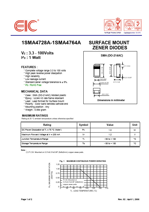
Note : (1) P.C.B. Mounted on 0.31x0.31x0.08" (8x8x2mm) copper areas pads.
Fig. 1 PD, MAXIMUM DISSIPATION (WATTS) 1.25 1.00 0.75 0.50 0.25 0 0
MAXIMUM CONTINUOUS POWER DERATING
P.C.B. Mounted on 0.31x0.31x0.08" (8x8x2mm) copper areas pads
25
50
75
100
125
150
175
TL, LEAD TEMPERATURE (°C)
Page 1 of 2
Rev. 02 : April 1, 2005
Rating at 25 °C ambient temperature unless otherwise specified Nominal Zener
Maximum Zener Impedance IZK (mA) 1.0 1.0 1.0 1.0 1.0 1.0 1.0 1.0 1.0 0.5 0.5 0.5 0.25 0.25 0.25 0.25 0.25 0.25 0.25 0.25 0.25 0.25 0.25 0.25 0.25 0.25 0.25 0.25 0.25 0.25 0.25 0.25 0.25 0.25 0.25 0.25 0.25
菲尼克斯型号
菲尼克斯电气中国公司隶属于德国菲尼克斯电气集团。
1928年,菲尼克斯电气发明了世界上第一片组合式接线端子,这就是现代端子的雏形,也是菲尼克斯电气申请并获得的第一个发明专利。
此后,菲尼克斯电气激情创新,致力于各种连接技术的开发,形成了完善的电气接口技术体系,其中很多产品系列已经成为行业的应用标准。
菲尼克斯电气中国公司植根中国大地,努力开拓自己的业务。
如今中国公司的业务发展迅速,已经成为整个集团全球业务的重要基石。
2004年集团提出了新的战略,中国公司与德国、美国公司一起成为集团的核心竞争力中心,技术支持和管理范围拓展到亚洲太平洋地区。
MACX MCR-EX-SL-RPSSI-IMACX MCR-SL-CAC-5-IMACX MCR-SL-CAC-5-I-UPMCR-1CLP-I-I-00MCR-2CLP-I-I-00MCR-4CLP-I-I-00MCR-C-I-I-00-DCMCR-C-I-I-04-DCMCR-C-I-I-40-DCMCR-C-I-U-0-DCMCR-C-I-U-4-DCMCR-CLP-UI-I-4MCR-CPS-I-I-44-EMCR-CPSS-I-I-44-EMCR-C-UI/UI-DCIMCR-C-U-I-0-DCMCR-C-U-I-10B-0B-DCIMCR-C-U-I-4-DCMCR-C-UI-UI-DCI-NCMCR-C-U-U-DCMCR-FL-C-UI-2UI-DCIMCR-FL-C-UI-2UI-DCI-NCMCR-FL-C-UI-UI-DCI-24/230MCR-F-UI-DCMCR-PS- 24DC/24DC/200MCR-PS- 24DC/2X24DCMCR-PS- 24DC-10DC MCR-PT 100-IMCR-PT100/I/DCMCR-PT100-UMCR-R-I-4-V-DCMCR-S-1/5-UI-DCIMCR-S-10/50-UI-DCI MCR-S10-50-UI-DCI-NC MCR-S-1-5-UI-SW-DCI-NC MCR-SL-1CLP-I-I-00-4KV MCR-SL-D-U-IMCR-SL-PT100-I-DC-24 MCR-SL-PT100-SPMCR-SL-S-1-5-I-DCI-230 MCR-SL-S-1-5-I-DCI-24 MCR-SL-S-16-SP-24 MCR-SWS-IMCR-SWS-UMCR-TE-JK-I-EMCR-T-UI-EMCR-T-UI-E-NCMCR-T-UI-NCMCR-VAC-UI-O-DCMCR-VDC-UI-B-DCMCV 1,5/ 2-G-3,5MCV 1,5/ 5-G-3,5MCV 1,5/ 8-G-3,5MCV 1,5/12-G-3,5 MCV 1,5/14-G-3,5MCV 1,5/16-G-3,5MCV 1.5/2-G-3.81MCV 1.5/6-GF-3.81 MCV 1.5/8-GF-3.81 MCVR 1.5/11-ST-3.81 MDSTB 2,5/10-G1-5,08 MDSTB 2,5/12-G1-5,08 MDSTB 2,5/20-G1-5,08ME 6,2 TBUS-2 1,5/5-ST-3,81 GN MINI MCR-SL-1CP-I-IMINI MCR-SL-2CP-I-IMINI MCR-SL-I-IMINI MCR-SL-PT100-UI-SPMINI MCR-SL-PTBMINI MCR-SL-RPS-I-IMINI MCR-SL-RPS-I-I-SPMINI MCR-SL-R-UIMINI MCR-SL-UI-2IMINI MCR-SL-UI-2I-NCMINI MCR-SL-UI-UIMINI MCR-SL-U-U-SPMINI-PS-100-240AC/ 5DC/3MINI-PS-100-240AC/10-15DC/2 MINI-PS-100-240AC/10-15DC/8 MINI-PS-100-240AC/24DC/MINI-PS-100-240AC/24DC/2MINI-PS-100-240AC/24DC/4MINI-PS-100-240AC/2X15DC/1 MINI-SYS-PS-100-240AC/24DC/1.5 PLC-BSC- 24DC/1/ACTPLC-BSC- 24DC/1/SENPLC-BSC- 24DC/21PLC-BSC- 24DC/21/SO46PLC-BSC- 24DC/21-21PLC-BSC- 24DC/21HCPLC-BSC- 24UC/21PLC-BSC- 24UC/21-21PLC-BSC- 48DC/21PLC-BSC- 48DC/21-21PLC-BSC- 48DC/21HCPLC-BSC-120UC/21-21/SO46PLC-BSC-230UC/1/SENPLC-BSC-230UC/21PLC-BSC-230UC/21/SO46PLC-BSC-230UC/21-21PLC-BSC-230UC/21-21/SO46 PLC-BSC-230UC/21HC/SO46 PLC-BSP- 24DC/1/ACTPLC-BSP- 24DC/21PLC-BSP- 24DC/21-21PLC-BSP- 48DC/21PLC-BSP- 48DC/21-21PLC-BSP-230UC/21/SO46PLC-ESK GYPLC-OSC- 24DC/24DC/2PLC-OSC- 24DC/48DC/100 PLC-OSC- 24DC/48DC/100/SEN PLC-OSC-230UC/48DC/100 PLC-OSP- 12DC/300DC/1PLC-OSP- 24DC/230AC/1PLC-OSP- 24DC/24DC/10PLC-OSP- 24DC/24DC/2PLC-OSP- 24DC/24DC/2/ACT PLC-RSC- 12DC/21PLC-RSC- 12DC/21-21PLC-RSC- 24DC/1/ACTPLC-RSC- 24DC/1-1/ACTPLC-RSC- 24DC/1IC/ACTPLC-RSC- 24DC/21PLC-RSC- 24DC/21-21PLC-RSC- 24DC/21AUPLC-RSC- 24DC/21HCPLC-RSC- 24UC/21PLC-RSC- 24UC/21-21PLC-RSC-120UC/21PLC-RSC-120UC/21-21PLC-RSC-230UC/1AU/SENPLC-RSC-230UC/21PLC-RSC-230UC/21/SO46PLC-RSC-230UC/21-21PLC-RSC-230UC/21-21/SO46 PLC-RSC-230UC/21HCPLC-RSP- 24DC/1/ACTPLC-RSP- 24DC/1AU/SENPLC-RSP- 24DC/21PLC-RSP-230UC/1/SENPLC-RSP-230UC/1AU/SENPLC-RSP-230UC/21PLC-RSP-230UC/21-21PLC-V8/FLK14/INPLC-V8/FLK14/OUTPND ADAPTER VGA USBPOWERSET BC/3/FM/PLUSPOWERSET BC/3+1/FMPOWERSET BC/3+1-100/FMPOWERSET-BC-CTRL/KYPPC 5315 PMPPS BASIC I/MPPS CD MPPS STANDARD I/MPR2-BSC3/4X21通用型初级开关电源2938578 QUINT-PS-100-240AC/24DC/2.5 2938581 QUINT-PS-100-240AC/24DC/5 2866255 QUINT-PS-100-240AC/48DC/5 2938594 QUINT-PS-3X400-500AC/24DC/5 2938811 QUINT-PS-100-240AC/12DC/10 2938604 QUINT-PS-100-240AC/24DC/10 2938248 QUINT-PS-100-240AC/48DC/10 2938617 QUINT-PS-3X400-500AC/24DC/10 2938219 QUINT-PS-3X400-500AC/48DC/10 2938620 QUINT-PS-100-240AC/24DC/20 2938976 QUINT-PS-100-240AC/48DC/20 2938727 QUINT-PS-3X400-500AC/24DC/ 20 2938222 QUINT-PS-3X400-500AC/48DC/20 2938633 QUINT-PS-3X400-500AC/24DC/30 2938879 QUINT-PS-100-240AC/24DC/40 2938646 QUINT-PS-3X400-500AC/24DC/40 2866378 QUINT-PS-24DC/24DC/102938196 QUINT-PS-ADAPTERS7/12938206 QUINT-PS-ADAPTERS7/22866857 QUINT-ADAPTER/42938235 UWA 182/52超薄设计的初级开关电源2938714 MINI-PS-100-240AC/ 5DC/3 2938743 MINI-PS-100-240AC/2X15DC/1 2938756 MINI-PS-100-240AC/10-15DC/2 2866297 MINI-PS-100-240AC/10-15DC/8 2938840 MINI-PS-100-240AC/24DC/1 2866446 MINI-PS-100-240AC/24DC/1.3 2938730 MINI-PS-100-240AC/24DC/2 2938837 MINI-PS-100-240AC/24DC/4 2866336 MINI-PS-100-240AC/24DC/C2LPS 2866271 MINI-PS-48-60DC/24DC/1 2866284 MINI-PS-12-24DC/24DC/1 2866983 MINI-SYS-PS-100-240AC/24DC/1.5 阶梯设计的初级开关电源2938918 STEP-PS-100-240AC/ 5DC/4 2938921 STEP-PS-100-240AC/12DC/3 2938934 STEP-PS-100-240AC/15DC/2.4 2938947 STEP-PS-100-240AC/24DC/1.5 2938950 STEP-PS-100-240AC/48DC/0.75菲尼克斯电压隔离转换模块2766821 MCR-PS- 24DC/24DC/2002781877 MCR-PS- 24DC/2X24DC2940676 EG 45-PS-230AC/ 5DC/250 2940618 EG 45-PS-230AC/24DC/250防爆型初级开关电源和冗余模块2938853 QUINT-PS-100-240AC/24DC/5/EX 2938866 QUINT-PS-100-240AC/24DC/10/EX 2938963 QUINT-DIODE/40菲尼克斯不间断初级开关电源2866213 QUINT-BUFFER/24DC/202866226 QUINT-DC-UPS/24DC/102866239 QUINT-DC-UPS/24DC/202866242 QUINT-DC-UPS/24DC/402866349 QUINT-BAT/24DC/3.4AH2866352 QUINT-BAT/24DC/7.2AH2866365 QUINT-BAT/24DC/12AH菲尼克斯初级开关电源单元2866268 TRIO-PS/1AC/24DC/2.52866310 TRIO-PS/1AC/24DC/52866323 TRIO-PS/1AC/24DC/102866459 TRIO-PS/3AC/24DC/102866381 TRIO-PS/1AC/24DC/202866394 TRIO-PS/3AC/24DC/202866404 TRIO-PS/3AC/24DC/40菲尼克斯电压调整模块2954963 EMG 45-NZG/G 5/SI2943903 EMG 30-NZG/G 5/SI2954976 EMG 45-NZG/G12/SI2943916 EMG 30-NZG/G12/SI2954992 EMG 45-NZG/G15/SI2943929 EMG 30-NZG/G15/SI2954989 EMG 45-NZG/G24/SI2943932 EMG 30-NZG/G24/SI2941060 EMG 75-NZG/G 5/22941057 EMG 75-NZG/G12/22941044 EMG 75-NZG/G15/22942454 EMG 75-NZG/G24/22736686 ASI QUINT 100-240/2.4 EFD2736699 ASI QUINT 100-240/4.8 EFD2943738 EMG 45-SD-D/LA/SI2940825 EMG 45-SD-D/LA/SI YE2941523 EMG 90-2SD-D/LA菲尼克斯防雷器、菲尼克斯浪涌保护器:菲尼克斯电源第一级防雷器2858467 AEC组合防雷器 POWERSET BC/3+1-100/FM1 2816881 电源第一级防雷器 FLT 35/3 通流量35KA(三相)2 2817482 电源第一级防雷器 FLT 35/3+1 通流量35KA(三相)3 2838940 电源第一级防雷器 FLT 35-260 通流量35KA(单相)4 2816904 电源第一级防雷器 FLT 50 N/PE 通流量50KA(N-E)5 2838160 电源第一级防雷器 FLT 100-260 通流量100KA(单相)6 2809717 电源第一级防雷器 FLT 25-400 通流量25KA7 2748603 电源第一级防雷器 FLT 60-400 通流量60KA8 2816386 电源第一级防雷器 FLT-PLUS 通流量50KA9 电源第一级防雷器 FLT 25-400/3+1 通流量50KA10 2856317 电源第一级防雷器 FLT 35/3+1 CTRL-0.9/I 通流量35KA(三相带指示灯)11 2856304 电源第一级防雷器 FLT 35/3 CTRL-0.9/I 通流量35KA(三相带指示灯)12 2817411 电源第一级防雷器 FLT 35 CTRL-0.9 通流量35KA(单相)13 2817424 电源第一级防雷器 FLT 35 CTRL-0.9/I 通流量35KA(单相,带指示灯)14 2817453 电源第一级防雷器 FLT 50 N/PE CTRL-1.5 通流量50KA(N-E)15 2818643 电源第一级防雷器 FLT-PLUS CTRL-0.9 通流量50KA,残压0.9KV16 2818960 电源第一级防雷器 FLT-PLUS CTRL-0.9/I 通流量50KA,残压0.9KV 电源第二级防雷器特价供应菲尼克斯电源,菲尼克斯安全栅,菲尼克斯端子,菲尼克斯继电器,大量库存.17 5772061 电源第二级防雷器 VAL-MS 320/1+1 通流量40KA单相8/20us、耐压320V18 5772074 电源第二级防雷器 VAL-MS 320/1+1-FM 同上、带遥信19 5772029 电源第二级防雷器 VAL-MS 230/1+1 通流量40KA单相8/20us、耐压275V20 5772032 电源第二级防雷器 VAL-MS 230/1+1-FM 同上、带遥信21 5772045 电源第二级防雷器 VAL-MS 230 IT/1+1 通流量40KA单相8/20us、耐压385V22 5772058 电源第二级防雷器 VAL-MS 230 IT/1+1-FM 同上、带遥信23 2838209 电源第二级防雷器 VAL-MS 230/3+1 通流量40KA三相8/20us24 2858548 电源第二级防雷器 VAL-MS 230 IT/3+1 通流量40KA三相8/20us25 2838199 电源第二级防雷器 VAL-MS 230/3+1 FM 通流量40KA(带遥信)三相8/20us26 2858551 电源第二级防雷器 VAL-MS 230 IT/3+1-FM 通流量40KA(带遥信)三相8/20us27 2858564 电源第二级防雷器 VAL-MS 320/3+1 通流量40KA三相8/20us28 2858577 电源第二级防雷器 VAL-MS 320/3+1-FM 通流量40KA三相8/20us29 直流48V防雷器 VAL-MS 60 通流量40KA(不带遥信)30 2817987 电源第二级防雷器 F-MS 12 通流量40KA(N-E)31 2817974 电源第二级防雷器 F-MS 12/FM 通流量40KA(N-E,带遥信)电源第三级防雷器32 2858357 电源第三级防雷器 PT 2-PE/S-230AC 通流量10KA、单相33 2839389 电源第三级防雷器 CBT-4MS 通流量5KA、4孔34 2762100 电源第三级防雷器 MT-4PE-230AC 通流量6.5KA、三相34 电源第三级防雷器 CBT-SCHUKO 通流量6.5KA、三相退耦器35 2749660 退耦器 LT35 额定电流35A36 2818546 退耦器 LT63 额定电流63A信号防雷器37 2839541 馈线防雷器 CF-UB-280DC-SB-SET 带接头38 2818148 馈线防雷器 CN-UB-280DC-SB N接头39 2809490 2M线防雷器 CN-UFB-5DC/E-LAN40 2782300 2M线防雷器 C-UFB-5DC/E2782313 C-UFB-24DC/E41 2838555 ISDN防雷器 CTM ISDN 插拔式42 2748276 ISDN防雷器 D-TR1/ISDN-A/RJ45-BB RJ4543 2838539 ADSL/电话线 CTM 1x2-110AC44 2838513 DDN CTM 1x2-24DC45 2838610 CTM接地架 CTM 10-MAG46 2765547 CTM接地架 CT 1-10-ES47 2818795 电话线防雷器 D-FM-A/RJ45-BB RJ45接口48 2838937 模拟电话信号 MT-2FM-RJ12 2路接口(RJ12接口)49 2858043 DDN/桢中继 PT3-HF-12DC-ST 插头,工作电压12V50 2856113 DDN/桢中继 PT 1x2-BE PT1*2底座51 2818973 以太网防雷器 D-LAN-A/RJ45-BS RJ45接口52 2838050 广域网防雷器 D-DS1-A/RJ45-BB53 2749644 无线收发设备防雷器 C-RF54 2818067 有线电视防雷器 CF-TV-30DC-BB F接口55 2749631 有线电视防雷器 C-TV DIN接口56 2762278 RS485 MT-RS485/S57 2782601 RS485 D-UFB-485/BS-B58 2796118 V.11/RS-422 D-UFB-V11/SB-B59 2762773 V.24/RS-232C D-UFB-V24/S-DSUB 9/SB-B60 2763701 视频信号防雷器 C-UB/E61 2782245 视频信号防雷器 C-UB62 2838050 T1/E1 D-DS1-A/RJ45-BB RJ45接口63 2838228 4-20mA模拟信号防雷器 PT 2x2-24DC-ST 通流量10KA(插头),2路保护UK1.5NUK1.5N BUUK2.5B UK2.5B BUUK3NUK3N BUUK 5NUK 5N BUUK 6NUK 6N BUUK 10NUK 10N BUUK 16NUK 16N BUUIK 35UIK 35 BUUK 35UKH 50UKH 50 BUUKH 95UKH 95 BUUKH 150UKH 150 BUUKH 240USLKG 1.5NUSLKG 2.5USLKG 3USLKG 5USLKG 6NUSLKG 10NUSLKG 16NUISLKG 35USLKG35USLKG50USLKG95UK 5-MTK-P/PUK 5-HESIUK 5-HSILED 24UK 5-HESILA 250 UK 10-DREHSI(5×20) URTK/SMBK 5/E-ZMBK 3/E-ZMBKKB 2.5UK 3-TWINUK 10-TWINUK 5-TWINUDK3UDK3-PEUDK4UDK4 BUUDK4-MTK-P/PUKK3UKK3 BUUKK5UKK5 BUDIK 1.5DIKD 1.5DOK 1.5URTKK 6-CAK4AK16AK35AKG 4 BUAKG 4 GNYEAKG 4 BKAKG 16 BUAKG 16 GNYEAKG 16 BKAKG 35 BUAKG 35 BKAZK 35D-URTKD-UK 2.5D-UK 4/10D-UK 16TS-RTKATS-RTKTS-KK3TS-KATP-UKATP-UK 5-MTKTP-UK35D-MBKKB 2.5DP-MBKKB2.5D-MBK/ED-UK 5-TWIND-UKK 3/5DP-UKK3/5DG-UKK3/5D-UDK4ATP-UKK3/5MPS-IH WHMPS-IH RDMPS-IH BUMPS-IH YEMPS-IH GNMPS-IH VTMPS-IH GYMPS-IH BKMPS-MTSAGK 10-UKH50AGK 10-UKH95AKG 10-UKH 150/240 UKH 50 EPUKH 150/240 EPFB10-6FB10-8FB10-10FB10-12FB2-15FB3-15FBRN 10-4NFBRI 2-5NFBRI 3-5NFBRI 4-5NFBRI 5-5NFBRI 10-5NFBRNI 2-5NFBRNI 3-5NFBRNI 10-5NFBI 2-6FBI 3-6FBI 5-6FBI 10-6FBI 2-8FBI 3-8FBI 5-8FBI 10-8FBI 2-10FBI 3-10 FBI 5-10 FBI 10-10FBI 10-12FB2-RTK/SFB3-RTK/SFB5-RTK/SFB10-RTK/SFBI 2-15FBI 3-15FBI 5-15FBI 2-20ISSBI 10-6ISSBI 10-10 ISSBI 10-8EB 10-5EB 3-5EB 2-5EBL 10-5EBL 2-5EBL 3-5EB 10-6EB 3-6EB 2-6EB 10-8EB 3-8EB 2-8EBS 10-8 EBS 3-8 EBS 2-8EB 10-10EB 3-10EB 2-10EB 10-12EB10-15EB 80-DIK BUEB 80-DIK RDSB 2-RTK/SSB 4-RTK/SUSB 2-RTK/SASB 2-RTK/SIS-K 4IS-K 10USBR 2-7KSS 6KSS 3-6 KSS 4-8 KSS 8RPSPS-IH WHPS-IH BUPS-IH YEPS-IH GNPS-IH VTPS-IH GYPS-IH BKPS-MTPSBJ 3/13/4 PSB 6/5/6 PSB 4/7/6PSB 3/10/4WS 3-6WS 3-8WS 4-6WS 4-8WS 4-15WS 5-6WS 5-8WS 5-15WS 3/4-UKH 50/25WS 4/5-UKH 50/25KLM-A+ES/KLM-GBUBE/D+ES/KMK3ST 1.5ST 1.5 BUST 2.5 ST 2.5 BUST4ST4 BUST6ST6 BUST10ST10 BUST16ST16 BUST35ST35 BUSTS2.5STS 2.5 BUSTS4 STS4 BUST1.5-PEST2.5-PEST4-PEST6-PEST 10-PEST 16-PEST 35-PESTS2.5-PESTS4-PEMZB1.5MZB1.5-NS35 MZDB1.5MZDB1.5-NS35MZB1.5-FMZB1.5-MMZDB1.5-FMZDB1.5-MMZB1.5-RZMZDB1.5-RZMZB1.5-PEMZB1.5-NS35-PEZRTK4ST1.5-TWINST2.5-TWINST4-TWIN ST6-TWINSTS2.5-TWINSTS4-TWINST1.5-QUATTROST2.5-QUATTROST4-QUATTROSTS4-QUATTROSTS2.5-QUATTROSTTB1.5STTB2.5STTB4ST1.5-TWIN-P E ST1.5-QUATTRO-PEST2.5-TWIN-PEST2.5-QUATTRO-PEST4-TWIN-PEST4-QUATTRO-PESTS4-TWIN-PESTS4-QUATTRO-PESTS2.5-TWIN-PESTS2.5-QUATTRO-PESTTB2.5-PEST2.5-MTST2.5-TGST4-HESI(5×20)ST2.5/1P ST2.5-QUATTRO/2P STTB2.5/2PSP2.5/1-LSP2.5/1-MSP2.5/1-RSPB2.5/1-LSPB2.5/1-MSPB2.5/1-RSPDB2.5/1-LSPDB2.5/1-MSPDB2.5/1-RFBS2-4FBS3-4FBS4-4FBS5-4FBS10-4FBS20-4 FBS2-5FBS3-5FBS4-5FBS5-5FBS10-5FBS20-5FBS2-6FBS3-6FBS4-6FBS5-6FBS10-6FBS20- FBS2-8FBS3-8FBS4-8FBS5-8FBS10-8FBS2-10FBS2-12FBS2-16D-MZB1.5D-MZB1.5-FD-MZB1.5-NS35D-ST2.5D-ST4D-ST6D-ST10D-ST16D-STS2.5D-STS4D-ST2.5-TWIND-ST4-TWIND-ST2.5-QUATTROD-ST4-QUATTROD-STTB2.5D-STTB4D-ZRTK4DS-ST2.5DS-ST4ATP-ST4ATP-ST4 QUATTROZB空白标识条ZB:数字标识条普通(1-100)ZB:数字标识条特殊打印ZBFM4/WH:UNBEDRUCKT ZBFM5/WH:UNBEDRUCKT ZBFM6/WH:UNBEDRUCKTZBFM4:SO/CMSZBFM5:SO/CMSZBFM6:SO/CMSZBFM7:SO/CMSB-STIFT 记号笔NS35/7.5 1M PERFORATED NS35/7.5 1M UNPERFORATED NS15 GELOCHT METER(带孔) NS15 UNGELOCHT METERNS32 GELOCHT METERNS32 UNGELOCHT METERNS35/7.5 UNGELOCHT METER NS35/7.5 GELOCHT METER NS35/15 UNGELOCHT METER NS35/15 GELOCHT METER NLS-CU3/10 1ME/UK1E/UKE/AL-NS32E/AL-NS35CLIPFIX35AB/SSAP2 METERAP3 METERAP2-TUAP3-TUAP-ESAI0.5-8WHAI0.75-8BU AI 1-8RDAI 1.5-8BKAI2.5-8GYAI4-10OGAI6-12GNAI10-12BNAI16-12WHAI25-16BKAI35-16RDAI50-20BUAI120-27BUAI70-20YEAI95-25RDAI-TWIN 2×0.75-8GYAI-TWIN 2×1-8RDAI-TWIN 2×1.5-8BKAI-TWIN 2×2.5-10BUAI-TWIN 2×4-12GYCUTFOX EBCUTFOX FBCUTFOX35PPS STANDARD I/MPPS BASIC I/MCRIMPFOX ZA 3CRIMPFOX UD 6-4CRIMPFOX UD 10-4CRIMPFOX UD 6-6CRIMPFOX INC 6 CRIMPFOX-4.0-ED-2.50 CF3000-2.5ZAP 25TZAP 100TSZF 1-0.6X3.5QUICK-WIREFOX6QUICK-WIREFOX 2.5CYCLOPSNS 15 PERFORATED 1MNS 15 UNPERFORATED 1MNS 35/7.5 PERFORATED 1MNS 35/7.5 UNPERFORATED 1MNS 32 PERFORATED 1MNS 32 UNPERFORATED 1MNS 35/15 PERFORATED 1MNS 35/15 UNPERFORATED 1MOTTA2.5OTTA6OTTA6-P/P OTTA6-T-P/POTTA6-TOTTA 6-PEOTTA2.5-PEOTTA2.5-P/POTTA25-M5OTTA25-M6UK35 BUURTK6D-OTTA2.5D-OTTA25D-OTTA6D-OTTA6-TATP-OTTAUT2.5UT2.5 BUUT2.5-PEUT2.5/1PUT2.5/1P BUUT2.5/1P-PEUT4UT4 BUUT4-PE UT4-DIO/L-R UT4-DIO/R-LUT4-HEDIUT4-HEDI BUUT4-HEDI-P/PUT4-HESI(5×20)UT4-HESILA 250UT4-HESILED 24UT4-HESILED 60UT4-MTUTF-MT BU UT4-MTD BU UT4-MTD-DIO/L-R-P/P UT4-MTD-DIO/R-L-P/P UT4-MTD-PEUT4-MTD-PE/SUT4-MT-P/PUT4-MT-P/P BUUT4-MT-P/P OGUT4-TGUT4-TG-P/PUT6UT6 BUUT6-PEUT10UT10 BUUT10-PEUT16 UT16 BUUT16-PEUT35UT35 BUUT35-PED-UT 2.5/10D-UT 2.5/1PD-UT16ATP-UTQTC1.5QTC1.5 BUQTC1.5-PEQTC1.5-QUATTRO QTC1.5-QUATTRO BU QTC1.5-QUATTRO-PE QTC1.5-TWINQTC1.5-TWIN BU QTC1.5-TWIN-PE QTC2.5QTC2.5 BUQTC2.5-PEQTC2.5-TWINQTC2.5-TWIN BU QTC2.5-TWIN-PED-QTC1.5D-QTC1.5-QUATTRO D-QTC1.5-TWIND-QTC2.5D-QTC2.5-TWINATP-QTCATP-QTC QUATTROATP-QTC TWINATP-QTTCBHDFK10 HDFKV10HDFK16HDFKV16HDFK25HDFKV25HDFK95HDFKV95HDFK4HDFKV4HDFK50HDFKV50ST4-HESILED24(5X20)ST4-HESILED24(6.3X32)MC1.5/2-GF-3.81MCV1.5/2-GF-3.81MC1.5/2-STF-3.81MC1.5/3-GF-3.81MCV1.5/3-GF-3.81MC1.5/3-STF-3.81MC1.5/4-GF-3.81MCV1.5/4-GF-3.81MC1.5/4-STF-3.81MC1.5/5-GF-3.81MCV1.5/5-GF-3.81MC1.5/5-STF-3.81MC1.5/6-GF-3.81MCV1.5/6-GF-3.81MC1.5/6-STF-3.81MC1.5/7-GF-3.81MCV1.5/7-GF-3.81 MC1.5/7-STF-3.81 MC1.5/8-GF-3.81MCV1.5/8-GF-3.81MC1.5/8-STF-3.81MC1.5/9-GF-3.81MCV1.5/9-GF-3.81MC1.5/9-STF-3.81MC1.5/10-GF-3.81MCV1.5/10-GF-3.81MC1.5/10-STF-3.81MC1.5/11-GF-3.81 MCV1.5/11-GF-3.81 MC1.5/11-STF-3.81MC1.5/12-GF-3.81MCV1.5/12-GF-3.81MC1.5/12-STF-3.81MC1.5/13-GF-3.81MCV1.5/13-GF-3.81MC1.5/13-STF-3.81MC1.5/14-GF-3.81MCV1.5/14-GF-3.81MC1.5/14-STF-3.81MC1.5/15-GF-3.81MCV1.5/15-GF-3.81MC1.5/15-STF-3.81MC1.5/16-GF-3.81MCV1.5/16-GF-3.81MC1.5/16-STF-3.81UTA159 MSTBV2.5/6-GF-5.08 MVSTBR2.5/6-STF-5.08MSTBV2.5/7-STF-5.08MUSTBR2.5/7-STF-5.08MSTBV2.5/11-GF-5.08MVSTBR2.5/11-STF-5.08MSTBV2.5/20-GF-5.08MVSTBR2.5/20-STF-5.08MDSTBV2.5/16-GF-5.08UMSTBVK2.5/2-G-5.08UMSTBVK2.5/3-G-5.08DFK-MSTB2.5/6-G-5.08DFK-MSTB2.5/10-G-5.08UMK-SE-11.25DFK-MSTB2.5/10-GF-5.08FRONT4-H-7.62MDSTB2.5/2-GFL-5.08MDSTB2.5/2-GFR-5.08AI-TWIN2*0.5-8WHAI0.5-6WH REL-MR-12DC/21REL-MR-24DC/21PLC-OSC-24DC/24DC/2PLC-BSC-24DC/21QUINT-PS-100-240AC/24DC/10 QUINT-PS-100-240AC/24DC/5PLC-RSC-48DC/21-21PLC-BSP-24DC/21(底座)PLC-RSP-24DC/21PLC-BSC-230UC/21(底座)DPT-24DC/24DC/2PLC-OSC-230UC/48DC/100MPS-MTMPS-1H-RDSZS0.6*3.5URTK/S-BEN ST2.5-QUATTRO-DI0/L-R MBKKB2.5-DI0/0-UKMKKMK2KMK3KMK4UKKB10ZDMTK 2.5ZDMTK 2.5 BUST-BEUK4-TGAI0.75-6GYAI2.5-8BUAI6-12YEMBK2.5/EST2.5-QUATTRO BU ST4-QUATTRO BUMZB1.5-MMZB1.5-F MBK 5/E-TG UBE+ES/KMK3SZF0-0.4*2.5SZF2-0.8*4.01B 1L AO 1/SFSZS0.4*2.5UK10-PLUSUK10-DREHSI(6.3*32) ZFK6-DREHSI(6.3*32) ESL 40*17DP-UKK3/5DG-UKK3/5MTK-P/PST6-TWIN BUD-ST6 TWIN ST6-TWIN AI1.5-10BKMKDSN1.5/2-5.08 MKDSN1.5/3-5.08 MKDS1.5/2-5.08 MKDS1.5/3-5.08 MKDS3/2-5.08MKDS3/3-5.08 MKDSP1.5/2-5.08 MKDSP1.5/3-5.08 SMKDSP1.5/2-5.08 SMKDSP1.5/3-5.08 MKKDSN1.5/2-5.08 MKKDSN1.5/3-5.08 MKKDS1.5/2-5.08 MKKDS1.5/3-5.08 MKKDS3/2-5.08 MKKDS3/3-5.08 GMKDS1.5/2-7.62 GMKDS1.5/3-7.62GMKDS3/2-7.62GMKDS3/3-7.62FRONT2.5-H/SA5D-FRONT2.5-V-O.Z.D-FRONT2.5-H-O.Z.FRONT2.5-V/SA5FFKDS/V-2.54FFKDS/H-2.54FFKDSA1/V-5.08FFKDSA1/H-5.08FFKDS/V-3.81FFKDS/H-3.81FFKDSA1/V-6.35FFKDSA1/H-6.35FFKDS/V1-5.08FFKDS/H1-5.08 FFKDSA1/1V-7.62 FFKDSA1/H1-7.62FFKDSA/H1-7.62FFKDSA/V1-7.62ZFKDS1-3.81ZFKDSA1-6.35ZFKDS1.5-5.08ZFKDSA1.5-7.62ZFKKDS1.5-5.08ZFKKDSA1.5-6.08ZFKDS1.5C-5.0ZFKDSA1.5C-6.0ZFKKDS1.5C-5.0ZFKKDSA1.5C-5.0LZFKKDSA1.5C-6.0RZFKDS2.5-5.08ZFKDS2.5-5.08LZFKDSA2.5-6.08RZFKKDS2.5-5.08ZFKKDSA2.5-6.08RZFKKDS2.5-5.08LZFKDS4-7.5ZFKDS4-10ZFKDSA4-9MC1.5/2-ST-3.81 MC1.5/3-ST-3.81 MC1.5/4-ST-3.81MC1.5/5-ST-3.81MC1.5/6-ST-3.81MC1.5/7-ST-3.81MC1.5/8-ST-3.81MC1.5/9-ST-3.81MC1.5/10-ST-3.81MC1.5/11-ST-3.81MC1.5/12-ST-3.81MC1.5/13-ST-3.81MC1.5/14-ST-3.81MC1.5/15-ST-3.81MC1.5/16-ST-3.81MC1.5/2-G-3.81MC1.5/3-G-3.81MC1.5/4-G-3.81MC1.5/5-G-3.81MC1.5/6-G-3.81MC1.5/7-G-3.81MC1.5/8-G-3.81MC1.5/9-G-3.81MC1.5/10-G-3.81MC1.5/11-G-3.81MC1.5/12-G-3.81MC1.5/13-G-3.81MC1.5/14-G-3.81MC1.5/15-G-3.81MC1.5/16-G-3.81MCV1.5/2-G-3.81MCV1.5/3-G-3.81MCV1.5/4-G-3.81MCV1.5/5-G-3.81MCV1.5/6-G-3.81MCV1.5/7-G-3.81MCV1.5/8-G-3.81MCV1.5/9-G-3.81MCV1.5/10-G-3.81MCV1.5/11-G-3.81MCV1.5/12-G-3.81MCV1.5/13-G-3.81MCV1.5/14-G-3.81MCV1.5/15-G-3.81MCV1.5/16-G-3.81MSTB2.5/2-ST-5.08MSTB2.5/3-ST-5.08MSTB2.5/4-ST-5.08MSTB2.5/5-ST-5.08MSTB2.5/6-ST-5.08MSTB2.5/7-ST-5.08MSTB2.5/8-ST-5.08MSTB2.5/9-ST-5.08MSTB2.5/10-ST-5.08MSTB2.5/11-ST-5.08MSTB2.5/12-ST-5.08MSTB2.5/13-ST-5.08MSTB2.5/14-ST-5.08MSTB2.5/15-ST-5.08MSTB2.5/16-ST-5.08 MSTB2.5/17-ST-5.08 MSTB2.5/18-ST-5.08MSTB2.5/19-ST-5.08MSTB2.5/20-ST-5.08MVSTBR2.5/2-ST-5.08MVSTBR2.5/3-ST-5.08MVSTBR2.5/4-ST-5.08MVSTBR2.5/5-ST-5.08MVSTBR2.5/6-ST-5.08MVSTBR2.5/7-ST-5.08MVSTBR2.5/8-ST-5.08MVSTBR2.5/9-ST-5.08MVSTBR2.5/10-ST-5.08MVSTBR2.5/11-ST-5.08MVSTBR2.5/12-ST-5.08MVSTBR2.5/13-ST-5.08MVSTBR2.5/14-ST-5.08MVSTBR2.5/15-ST-5.08MVSTBR2.5/16-ST-5.08MVSTBW2.5/2-ST-5.08MVSTBW2.5/3-ST-5.08MVSTBW2.5/4-ST-5.08MVSTBW2.5/5-ST-5.08 MVSTBW2.5/6-ST-5.08 MVSTBW2.5/7-ST-5.08MVSTBW2.5/8-ST-5.08MVSTBW2.5/9-ST-5.08MVSTBW2.5/10-ST-5.08MVSTBW2.5/11-ST-5.08MVSTBW2.5/12-ST-5.08MVSTBW2.5/13-ST-5.08MVSTBW2.5/14-ST-5.08MVSTBW2.5/15-ST-5.08MVSTBW2.5/16-ST-5.08FKC2.5/2-ST-5.08FKC2.5/3-ST-5.08FKC2.5/4-ST-5.08FKC2.5/5-ST-5.08FKC2.5/6-ST-5.08FKC2.5/7-ST-5.08FKC2.5/8-ST-5.08FKC2.5/9-ST-5.08FKC2.5/10-ST-5.08FKC2.5/11-ST-5.08FKC2.5/12-ST-5.08 FKC2.5/13-ST-5.08 FKC2.5/14-ST-5.08FKC2.5/15-ST-5.08FKC2.5/16-ST-5.08MSTBA2.5/2-G-5.08MSTBA2.5/3-G-5.08MSTBA2.5/4-G-5.08MSTBA2.5/5-G-5.08MSTBA2.5/7-G-5.08MSTBA2.5/8-G-5.08MSTBA2.5/9-G-5.08MSTBA2.5/10-G-5.08MSTBA2.5/11-G-5.08MSTBA2.5/12-G-5.08MSTBA2.5/13-G-5.08MSTBA2.5/14-G-5.08MSTBA2.5/15-G-5.08MSTBA2.5/16-G-5.08MSTBA2.5/17-G-5.08MSTBA2.5/18-G-5.08MSTBA2.5/19-G-5.08MSTBA2.5/20-G-5.08MSTBVA2.5/2-G-5.08MSTBVA2.5/3-G-5.08MSTBVA2.5/4-G-5.08MSTBVA2.5/5-G-5.08MSTBVA2.5/6-G-5.08MSTBVA2.5/7-G-5.08MSTBVA2.5/8-G-5.08MSTBVA2.5/9-G-5.08MSTBVA2.5/10-G-5.08MSTBVA2.5/11-G-5.08MSTBVA2.5/12-G-5.08MSTBVA2.5/13-G-5.08MSTBVA2.5/14-G-5.08MSTBVA2.5/15-G-5.08MSTBVA2.5/16-G-5.08MSTBVA2.5/17-G-5.08MSTBVA2.5/18-G-5.08MSTBVA2.5/19-G-5.08MSTBVA2.5/20-G-5.08GMSTB2.5/2-ST-7.62 GMSTB2.5/3-ST-7.62 GMSTB2.5/4-ST-7.62GMSTB2.5/5-ST-7.62GMSTB2.5/7-ST-7.62GMSTB2.5/8-ST-7.62GMSTB2.5/9-ST-7.62GMSTB2.5/10-ST-7.62GMSTB2.5/11-ST-7.62GMSTB2.5/12-ST-7.62GMSTBA2.5/2-G-7.62GMSTBA2.5/3-G-7.62GMSTBA2.5/4-G-7.62GMSTBA2.5/5-G-7.62GMSTBA2.5/6-G-7.62GMSTBA2.5/7-G-7.62 GMSTBA2.5/8-G-7.62 GMSTBA2.5/9-G-7.62GMSTBA2.5/10-G-7.62GMSTBA2.5/11-G-7.62GMSTBA2.5/12-G-7.62GMSTBVA2.5/2-G-7.62GMSTBVA2.5/3-G-7.62GMSTBVA2.5/4-G-7.62GMSTBVA2.5/5-G-7.62GMSTBVA2.5/6-G-7.62GMSTBVA2.5/7-G-7.62GMSTBVA2.5/8-G-7.62GMSTBVA2.5/9-G-7.62GMSTBVA2.5/10-G-7.62GMSTBVA2.5/11-G-7.62GMSTBVA2.5/12-G-7.62CR-MSTBCP-MSTBSK U/2.8 WH:UNBEDRUCKTSK U/3.8 WH:UNBEDRUCKTSK 5/3.8:UNBEDRUCKTSK 5.08/3.8:UNBEDRUCKTME12.5UT GNME12.5OT-MSTBO SETME12.5OT-MKDSO SETME17.5UT GNME17.5OT-MSTBO SETME17.5OT-MKDSO SETME22.5UT GNME22.5OT-MSTBO SETME22.5OT-MKDSO SETUM72-PROFIL 200CMUM72-SEUM72-SEFE/LUM72-SEFE/RUM72-FEHC-B 6-EBUSHC-B 6-ESTSHC-B 10-EBUSHC-B 10-ESTSHC-B 16-EBUSHC-B 16-ESTSHC-B 24-EBUSHC-B 24-ESTSHC-B 6-TFL-43/M1PG13.5SHC-B 6-AMLHC-B 10-TFQ-52/M1PG16SHC-B 10-AMQHC B 16-TFQ-76/M1PG21SHC-B 16-AMQHC-B 24-AMQHC-B 24-TFQ-76/M1PG21SHC-B 48-TFL-96/M1PG29SHC-B 48-AML HC-B 32-TFQ-80/M1PG29S HC-B 32-AMQHC-D 25-EBUCHC-D 25-ESTCHC-D 40-EBUCHC-D 40-ESTCHC-A 10-ESTSHC-A 10-EBUSHC-A 3-ESTSHC-A 3-EBUSHC-A 4-EBUSHC-A 4-ESTSHC-D 7-AML-24/GR ALUHC-D 7-TFL-48/M1PG11G ALUHC-D 15-TFL-66/M1PG16SHC-D 15-AMLHC-D 25-TFL-72/M1PG16SHC-D 25-AMLHC-D 50-TFQ-76/M1PG29SHC-D 50-AMQHC-A 16-EBUSHC-A 16-ESTS CK1.6-ED-0.75ST AG CK1.6-ED-1.00ST AGCK1.6-ED-1.50ST AGCK1.6-ED-0.75BU AGCK1.6-ED-1.00BU AGCK1.6-ED-1.50BU AGSACB-4/4-L-CSACB-4/8-L-CSACB-8/8-L-CSACB-8/16-L-CSACB-4/4-CSACB-4/8-CSACB-8/8-CSACB-8/16-CSACB-4/4-L-C-90SACB-4/8-L-C-90SACB-8/8-L-C-90SACB-8/16-L-C-90SACB-4/4-C 90SACB-4/8-C 90SACB-8/8-C 90SACB-8/16-C 90SACB-4/8-5.0PURSACB-4/8-10.0PURSACB-8/16-5.0PURSACB-4/4-5.0PURSACB-4/4-10.0PURSACB-8/8-5.0PUR SACB-8/8-10.0PUR SACB-4/4-L-5.0PURSACB-4/4-L-10.0PURSACB-4/8-L-5.0PURSACB-4/8-L-10.0PURSACB-8/8-L-5.0PURSACB-8/8-L-10.0PURSACB-8/16-L-5.0PURSACB-8/16-L-10.0PURSACB-4/4-L-SCSACB-8/8-L-SCSACB-4/8-L-SCSACB-8/16-L-SCSACB-4/4-SCSACB-8/8-SCSACB-4/8-SC SACB-8/16-SCSACB-4Q/4P-5.0PURSACB-4Q/4P-10.0PURSACB-8Q/4P-5.0PURSACB-8Q/4P-10.0PURSACB-4Q/4P-L-5.0PURSACB-4Q/4P-L-10.0PURSACB-8Q/4P-L-5.0PURSACB-8Q/4P-L-10.0PURSACB-4Q/4P-L-SCSACB-8Q/4P-L-SCSACB-4Q/4P-SCSACB-8Q/4P-SCSACB-4/4-L-M23SACB-4/8-L-M23SACB-8/8-L-M23SACB-8/16-L-M23 SACB-4/4-L-M23 180 SACB-4/8-L-M23 180SACB-8/8-L-M23 180SACB-4/4-M23 180SACB-4/8-M23 180SACB-8/8-M23 180SACB-8/16-M23 180SACB-4/4-M23 SACB-4/8-M23 SACB-8/8-M23SACB-8/16-M23SAC-3P-M12MS/1.5-PURSAC-3P-M12MS/3.0-PURSAC-3P-M12MS/5.0-PURSAC-3P-M12MR/1.5-PURSAC-3P-M12MR/3.0-PURSAC-3P-M12MR/5.0-PURSAC-3P-M12MS/1.5-PUR/M 8FS SAC-3P-M12MS/3.0-PUR/M 8FS SAC-3P-M12MS/1.5-PUR/M 8FR SAC-3P-M12MS/3.0-PUR/M 8FR SAC-3P-M12MR/1.5-PUR/M 8FS SAC-3P-M12MR/3.0-PUR/M 8FS SAC-3P-M12MR/1.5-PUR/M 8FR SAC-3P-M12MR/3.0-PUR/M 8FR SAC-3PQ-1.5-PUR/M 8FSSAC-3PQ-3.0-PUR/M 8FS SAC-3PQ-5.0-PUR/M 8FSSAC-3PQ-1.5-PUR/M 8FRSAC-3PQ-3.0-PUR/M 8FRSAC-3PQ-5.0-PUR/M 8FRSAC-3P-M12MS/1.5-PUR/M12FS SAC-3P-M12MS/3.0-PUR/M12FS SAC-3P-M12MS/1.5-PUR/M12FR SAC-3P-M12MS/3.0-PUR/M12FR SAC-3P-1.5-PUR/M12FSSAC-3P-3.0-PUR/M12FSSAC-3P-1.5-PUR/M12FRSAC-3P-3.0-PUR/M12FRSAC-3P-5.0-PUR/M12FRSAC-4P-M12MS/1.5-PURSAC-4P-M12MS/3.0-PURSAC-4P-M12MS/5.0-PURSAC-4P-1.5-PUR/M12FSSAC-4P-3.0-PUR/M12FSSAC-4P-5.0-PUR/M12FSSAC-4P-M12MR/1.5-PURSAC-4P-M12MR/3.0-PURSAC-4P-M12MR/5.0-PURSAC-4P-1.5-PUR/M12FRSAC-4P-3.0-PUR/M12FRSAC-4P-5.0-PUR/M12FRSAC-4P-M12MS/1.5-PUR/M12FS SAC-4P-M12MS/3.0-PUR/M12FS SAC-4P-M12MS/1.5-PUR/M12FR SAC-4P-M12MS/3.0-PUR/M12FR SAC-4P-M12MR/1.5-PUR/M12FS SAC-4P-M12MR/3.0-PUR/M12FS SAC-4P-M12MR/1.5-PUR/M12FR SAC-4P-M12MR/3.0-PUR/M12FR SAC-4P-M12MS/1.5-PUR/M 8FS SAC-4P-M12MS/3.0-PUR/M 8FS SAC-5P-M12MS/1.5-PURSAC-5P-M12MS/3.0-PURSAC-5P-M12MS/5.0-PURSAC-5P-M12MR/1.5-PURSAC-5P-M12MR/3.0-PURSAC-5P-M12MR/5.0-PURSAC-5P-1.5-PUR/M12FSSAC-5P-3.0-PUR/M12FSSAC-5P-5.0-PUR/M12FSSAC-5P-1.5-PUR/M12FRSAC-5P-3.0-PUR/M12FRSAC-5P-5.0-PUR/M12FRSAC-5P-M12MS/1.5-PUR/M12FS SAC-5P-M12MS/3.0-PUR/M12FS SAC-5P-M12MS/1.5-PUR/M12FRSAC-5P-M12MS/3.0-PUR/M12FR SACC-M 8MS-3CON-M-SW SACC-M 8MS-4CON-M-SW SACC-M 8MS-3PCONSACC-M 8MS-4PCONSACC-M12MS-4CON-PG 7-M SACC-M12MS-5CON-PG 7-M SACC-M12MR-5CON-PG 7-M SACC-M12MR-4CON-PG 7-M SACC-M 8MS-3CON-MSACC-M 8MS-4CON-MSACC-M12MS-5CON-PG9-M SACC-M12MR-5CON-PG9-M SACC-M 8MR-3CON-MSACC-M 8FS-3PCONSACC-M 8FS-4PCONSACC-M 8FS-3CON-M-SW SACC-M 8FS-4CON-M-SW SACC-M12FS-5CON-PG 7-M SACC-M12FR-5CON-PG 7-M SACC-M12FS-4CON-PG 7-M SACC-M12FR-4CON-PG 7-M SACC-M 8FS-3CON-MSACC-M 8FS-4CON-MSACC-M12FS-5CON-PG9-M SACC-M12FR-5CON-PG9-M SACC-DSIV-M12MS-5CON-L180 SACC-DSIV-M12MS-5CON-L90 SACC-DSIV-M12FS-5CON-L180 SACC-DSIV-M12FS-5CON-L90 SACC-DSI-M12MS-5CON-L180 SACC-DSI-M8MS-3CON-L180 SACC-DSI-M8MS-4CON-L180 SACC-DSI-M12FS-5CON-L180 SACC-DSI-M8FS-3CON-L180 SACC-DSI-M8FS-4CON-L180 SAC-3P-5.0-PUR/M 8FSSAC-3P-5.0-PUR/M 8FRSAC-3P-1.5-PUR/M 8FSSAC-3P-3.0-PUR/M 8FSSAC-3P-1.5-PUR/M 8FRSAC-3P-3.0-PUR/M 8FRSAC-3P-M 8MS/1.5-PURSAC-3P-M 8MS/3.0-PURSAC-3P-M 8MS/5.0-PURSAC-3P-M 8MR/1.5-PURSAC-3P-M 8MR/3.0-PURSAC-3P-M 8MR/5.0-PURSAC-3P-M 8MS/1.5-PUR/M 8FS SAC-3P-M 8MS/3.0-PUR/M 8FS SAC-3P-M 8MS/1.5-PUR/M 8FR SAC-3P-M 8MS/3.0-PUR/M 8FR SAC-3P-M 8MS/1.5-PUR/M 12FS SAC-3P-M 8MS/3.0-PUR/M 12FS SAC-3P-M 8MS/1.5-PUR/M 12FR SAC-3P-M 8MS/3.0-PUR/M 12FR SAC-4P-M 8MS/1.5-PURSAC-4P-M 8MS/3.0-PURSAC-4P-M 8MS/5.0-PURSAC-4P-M 8MR/1.5-PURSAC-4P-M 8MR/3.0-PURSAC-4P-M 8MR/5.0-PURSAC-4P-1.5-PUR/M 8FSSAC-4P-3.0-PUR/M 8FSSAC-4P-5.0-PUR/M 8FSSAC-4P-1.5-PUR/M 8FRSAC-4P-3.0-PUR/M 8FRSAC-4P-5.0-PUR/M 8FRRCK-TGUM/BL12/5.0PUR-URCK-TGUM/BL12/10.0PUR-U RCK-TWUM/BL12/5.0PUR-URCK-TWUM/BL12/10.0PUR-U RCK-TGUM/BL16+3/5.0PUR-U RCK-TGUM/BL16+3/10.0PUR-U。
1SMA5918BT3G中文资料

1SMA5913BT3 Series1.5 Watt PlasticSurface MountZener Voltage RegulatorsThis complete new line of 1.5 Watt Zener Diodes offers the following advantages.Features•Standard Zener Breakdown V oltage Range − 3.3 V to 68 V •ESD Rating of Class 3 (>16 kV) per Human Body Model •Flat Handling Surface for Accurate Placement •Package Design for Top Slide or Bottom Circuit Board Mounting •Low Profile Package•Ideal Replacement for MELF Packages•Pb−Free Packages are AvailableMechanical Characteristics:CASE:V oid-free, transfer-molded plasticFINISH:All external surfaces are corrosion resistant with readily solderable leadsMAXIMUM CASE TEMPERATURE FOR SOLDERING PURPOSES: 260°C for 10 secondsPOLARITY:Cathode indicated by molded polarity notch or cathode bandFLAMMABILITY RATING:UL 94 V−0 @ 0.125 inMAXIMUM RATINGSRating Symbol Value UnitDC Power Dissipation @ T L = 75°C, Measured Zero Lead Length (Note 1) Derate above 75°CThermal Resistance, Junction−to−LeadP DR q JL1.52050WmW/°C°C/WDC Power Dissipation @ T A = 25°C (Note 2) Derate above 25°CThermal Resistance, Junction−to−AmbientP DR q JA0.54.0250WmW/°C°C/WOperating and Storage Temperature Range T J, T stg−65 to+150°CStresses exceeding Maximum Ratings may damage the device. Maximum Ratings are stress ratings only. Functional operation above the Recommended Operating Conditions is not implied. Extended exposure to stresses above the Recommended Operating Conditions may affect device reliability.1. 1 in square copper pad, FR−4 board.2.FR−4 Board, using ON Semiconductor minimum recommended footprint.Device Package Shipping†ORDERING INFORMATION1SMA59xxBT3SMA5000/Tape & Reel1SMA59xxBT3G SMA(Pb−Free)5000/Tape & Reel†For information on tape and reel specifications, including part orientation and tape sizes, please refer to our T ape and Reel Packaging Specifications Brochure, BRD8011/D.See specific marking information in the device marking column of the Electrical Characteristics table on page 2 of this data sheet.DEVICE MARKING INFORMATIONELECTRICAL CHARACTERISTICS (T A = 25°C unlessotherwise noted, V F = 1.5 V Max. @ I F = 200 mA for all types)Symbol ParameterV Z Reverse Zener Voltage @ I ZT I ZT Reverse CurrentZ ZT Maximum Zener Impedance @ I ZT I ZK Reverse CurrentZ ZK Maximum Zener Impedance @ I ZK I R Reverse Leakage Current @ V R V R Reverse Voltage I F Forward Current V F Forward Voltage @ I F I ZMMaximum DC Zener CurrentELECTRICAL CHARACTERISTICS (T A = 25°C unless otherwise noted, V F = 1.5 V Max. @ I F = 200 mA for all types)Device* (Note 3)Device Marking Zener Voltage (Note 4)Zener Impedance Leakage CurrentI ZM V Z (Volts)@ I ZT Z ZT @ I ZTZ ZK @ I ZK I R @ V R Min Nom Max mA W W mA m A Volts mA(dc)1SMA5913BT3, G 813B 3.13 3.3 3.47113.610500 1.050 1.04551SMA5914BT3, G 814B 3.42 3.6 3.78104.29.0500 1.035.5 1.04171SMA5915BT3, G 815B 3.70 3.9 4.1096.17.5500 1.012.5 1.03851SMA5916BT3, G 816B 4.08 4.3 4.5287.2 6.0500 1.0 2.5 1.03491SMA5917BT3, G 817B 4.46 4.7 4.9479.8 5.0500 1.0 2.5 1.53191SMA5918BT3, G 818B 4.84 5.1 5.3673.5 4.0350 1.0 2.5 2.02941SMA5919BT3, G 819B 5.32 5.6 5.8866.9 2.0250 1.0 2.5 3.02681SMA5920BT3, G 820B 5.89 6.2 6.5160.5 2.0200 1.0 2.5 4.02421SMA5921BT3, G 821B 6.46 6.87.1455.1 2.5200 1.0 2.5 5.22211SMA5922BT3, G 822B 7.127.57.8850 3.04000.5 2.5 6.02001SMA5923BT3, G 823B 7.798.28.6145.7 3.54000.5 2.5 6.51831SMA5924BT3, G 824B 8.649.19.5641.2 4.05000.5 2.57.01651SMA5925BT3, G 825B 9.51010.537.5 4.55000.25 2.58.01501SMA5926BT3, G 826B 10.451111.5534.1 5.55500.250.58.41361SMA5927BT3, G 827B 11.41212.631.2 6.55500.250.59.11251SMA5928BT3, G 828B 12.351313.6528.87.05500.250.59.91151SMA5929BT3, G 829B 14.251515.75259.06000.250.511.41001SMA5930BT3, G 830B 15.21616.823.4106000.250.512.2941SMA5931BT3, G 831B 17.11818.920.8126500.250.513.7831SMA5932BT3, G 832B 19202118.7146500.250.515.2751SMA5933BT3, G 833B 20.92223.11717.56500.250.516.7681SMA5934BT3, G 834B 22.82425.215.6197000.250.518.2631SMA5935BT3, G 835B 25.652728.3513.9237000.250.520.6561SMA5936BT3, G 836B 28.53031.512.5267500.250.522.8501SMA5937BT3, G 837B 31.353334.6511.4338000.250.525.1451SMA5938BT3, G 838B 34.23637.810.4388500.250.527.4421SMA5939BT3, G 839B 37.053940.959.6459000.250.529.7381SMA5940BT3, G840B40.854345.158.7539500.250.532.7351SMA5941BT3, G 841B 44.654749.358.06710000.250.535.8321SMA5942BT3, G 842B 48.455153.557.37011000.250.538.8291SMA5943BT3, G 843B 53.25658.8 6.78613000.250.542.6271SMA5944BT3, G 844B 58.96265.1 6.010015000.250.547.1241SMA5945BT3, G 845B 64.66871.4 5.512017000.250.551.7223.Tolerance and Voltage Regulation Designation − The type number listed indicates a tolerance of ±5%.4.V Z limits are to be guaranteed at thermal equilibrium.*The “G” suffix indicates Pb−Free package available.Figure 1. Steady State Power DeratingFigure 2. V Z − 3.3 thru 10 VoltsT, TEMPERATURE (°C)Figure 3. V Z = 12 thru 68 VoltsP D , M A X I M U MP O W E R D I S S I P A T I O N (W A T T S )I Z , Z E N E R C U R R E N T (m A )Z Z , D Y N A M I C I M P ED A N CE (O H M S )1002468101010.1V Z , ZENER VOLTAGE (VOLTS)1001010.1010203040V Z , ZENER VOLTAGE (VOLTS)V Z , ZENER VOLTAGE (VOLTS)1001050Figure 4. Zener Voltage − 3.3 to 12 VoltsFigure 5. Zener Voltage − 12 to 68 Volts Figure 6. Effect of Zener VoltageI Z , Z E N E R C U R R E N T (m A )6070801086420−2−4V Z , ZENER VOLTAGE (VOLTS), T E M P E R A T U R E C O E F F I C I E N T (m V / C )°θV Z 10070503020101020305070100V Z , ZENER VOLTAGE (VOLTS), T E M P E R A T U R E C O E F F I C I E N T (m V / C )°θV ZPACKAGE DIMENSIONSSMACASE 403D−02ISSUE Cǒmm inchesǓSCALE 8:1*For additional information on our Pb−Free strategy and solderingdetails, please download the ON Semiconductor Soldering and Mounting Techniques Reference Manual, SOLDERRM/D.SOLDERING FOOTPRINT*DIM A MIN NOM MAX MINMILLIMETERS1.912.16 2.410.075INCHES A10.050.100.150.002b 1.27 1.45 1.630.050c 0.150.280.410.006D 2.29 2.60 2.920.090E 4.06 4.32 4.570.160L0.761.14 1.520.0300.0850.0950.0040.0060.0570.0640.0110.0160.1030.1150.1700.1800.0450.060NOM MAX 4.83 5.21 5.590.1900.2050.220H E STYLE 1:PIN 1.CATHODE (POLARITY BAND)2.ANODENOTES:1.DIMENSIONING AND TOLERANCING PER ANSI Y14.5M, 1982.2.CONTROLLING DIMENSION: INCH.3.403D−01 OBSOLETE, NEW STANDARD IS 403D−02.ON Semiconductor and are registered trademarks of Semiconductor Components Industries, LLC (SCILLC). SCILLC reserves the right to make changes without further notice to any products herein. SCILLC makes no warranty, representation or guarantee regarding the suitability of its products for any particular purpose, nor does SCILLC assume any liability arising out of the application or use of any product or circuit, and specifically disclaims any and all liability, including without limitation special, consequential or incidental damages.“Typical” parameters which may be provided in SCILLC data sheets and/or specifications can and do vary in different applications and actual performance may vary over time. All operating parameters, including “Typicals” must be validated for each customer application by customer’s technical experts. SCILLC does not convey any license under its patent rights nor the rights of others. SCILLC products are not designed, intended, or authorized for use as components in systems intended for surgical implant into the body, or other applications intended to support or sustain life, or for any other application in which the failure of the SCILLC product could create a situation where personal injury or death may occur. Should Buyer purchase or use SCILLC products for any such unintended or unauthorized application, Buyer shall indemnify and hold SCILLC and its officers, employees, subsidiaries, affiliates,and distributors harmless against all claims, costs, damages, and expenses, and reasonable attorney fees arising out of, directly or indirectly, any claim of personal injury or death associated with such unintended or unauthorized use, even if such claim alleges that SCILLC was negligent regarding the design or manufacture of the part. SCILLC is an Equal Opportunity/Affirmative Action Employer. This literature is subject to all applicable copyright laws and is not for resale in any manner.PUBLICATION ORDERING INFORMATION。
。册手户用机片单列系考参请标指数参细详
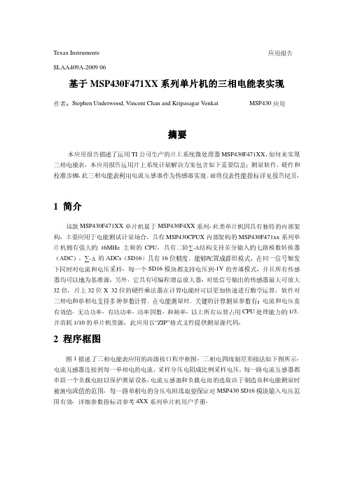
Texax Instruments 应用报告 SLAA409A-2009 06基于MSP430F471XX 系列系列单片机的三相电能单片机的三相电能单片机的三相电能表表实现作者:Stephen Underwood, Vincent Chan and Kripasagar Venkat MSP430应用摘要本应用报告描述了运用TI 公司生产的片上系统微处理器MSP430F471XX ,如何来实现三相电能表。
本应用报告运用片上系统计量解决方案包含如下重要信息:测量软件、硬件和校准步骤。
此三相电能表利用电流互感器作为传感器实现,最终仪表性能指标详见报告尾页。
1 简介这款MSP430F471XX 单片机属于MSP430F4XX 系列。
此类单片机因具有独特的内部架构,主要应用于电能测试计量场合。
具有MSP430CPUX 内部架构的MSP430F471xx 系列单片机拥有强大的16MHz 主频的CPU 。
具有二阶∑-∆结构支持差分输入的七路模数转换器(ADC )。
∑-∆ 的ADCs (SD16)具有16位精度,能够配置成群组模式,在同一信号触发下同时对电流和电压采样。
每一个SD16模块都支持电压到-1V 的普通模式,并且所有传感器均可以地为基准源。
另外,它具有可编程增益放大器,对低信号输出的传感器最大可放大32倍。
片上32位X 32位的硬件乘法器在计算电能时可以更加快速进行数学运算。
软件对三相电和单相电支持多种参数计算,在电能测量时,关键的计算测量参数有:电流和电压真有效值、无功功率、有功功率、功率因数、和频率。
以上所有运算占用CPU 处理能力的1/3,并消耗1/10的单片机资源。
此应用以“ZIP”格式文件提供测量源代码。
2 程序程序框图框图图1描述了三相电能表应用的高级接口程序框图。
三相电四线制星形接法如下图所示。
电流互感器连接到每一单相电的电流,采样分压电阻成比例采样电压。
每一路电流互感器都串联一个负载电阻以保护测量设备。
芯片pn551a参数

芯片pn551a参数全文共四篇示例,供读者参考第一篇示例:芯片PN551A是一款高性能、多功能的芯片,在电子产品中广泛应用。
它具有很多强大的参数和功能,下面我们来详细介绍一下它的各项参数。
芯片PN551A的尺寸为5mm x 5mm x 1mm,非常小巧,适合安装在各种小型电子产品中。
它采用了先进的工艺技术,具有高度集成的芯片结构,同时具备了高性能的处理能力和低功耗的特点。
芯片PN551A支持多种接口协议,包括I2C、SPI和UART等,使得它能够与不同类型的主控芯片进行通信,实现更加灵活的应用场景。
它还支持多种传输速率,可以满足不同产品的通信需求。
芯片PN551A具有丰富的功能模块,包括蓝牙、射频、NFC、USB等,涵盖了多种无线通信方式,能够实现蓝牙音频传输、数据传输、支付功能等多种应用场景。
它还具有强大的数据处理能力,能够实现实时的数据传输和处理,使产品性能更加优越。
芯片PN551A还具有丰富的安全功能,包括身份认证、加密解密、随机数生成等多种安全机制,可以保护产品的数据安全。
它还支持多种电源管理模式,能够实现低功耗的工作状态,延长产品的使用时间。
芯片PN551A是一款具有多项强大参数和功能的芯片,适用于各种小型电子产品中,能够满足不同需求的设计要求。
它具有高性能、低功耗、丰富的功能模块、多种通信接口、强大的数据处理能力和安全功能等特点,是一款非常值得推荐的芯片。
第二篇示例:芯片PN551A采用的是32位ARM Cortex-M4内核,运行主频可达到100MHz。
这样的高性能处理器可以保证芯片在进行复杂计算和数据处理时能够快速高效地完成任务。
低功耗设计也是芯片PN551A 的特点之一,可以在保证性能的同时延长电池续航时间,提高产品的使用体验。
芯片PN551A内置了多种接口和外设模块,例如USB接口、SPI 接口、I2C接口等,可以方便地与外部设备进行通信和数据交换。
芯片还内置了丰富的模拟和数字引脚,可以满足各种外部传感器和器件的连接需求。
LM1117IDTX-5.0中文资料

LM1117/LM1117I800mA Low-Dropout Linear RegulatorGeneral DescriptionThe LM1117is a series of low dropout voltage regulators with a dropout of 1.2V at 800mA of load current.It has the same pin-out as National Semiconductor’s industry standard LM317.The LM1117is available in an adjustable version,which can set the output voltage from 1.25V to 13.8V with only two external resistors.In addition,it is also available in five fixed voltages,1.8V,2.5V,2.85V,3.3V,and 5V.The LM1117offers current limiting and thermal shutdown.Its circuit includes a zener trimmed bandgap reference to as-sure output voltage accuracy to within ±1%.The LM1117series is available in LLP ,TO-263,SOT-223,TO-220,and TO-252D-PAK packages.A minimum of 10µF tantalum capacitor is required at the output to improve the transient response and stability.Featuresn Available in 1.8V,2.5V,2.85V,3.3V,5V,and Adjustable Versionsn Space Saving SOT-223and LLP Packages n Current Limiting and Thermal Protection n Output Current 800mA n Line Regulation 0.2%(Max)n Load Regulation 0.4%(Max)n Temperature Range —LM11170˚C to 125˚C —LM1117I −40˚C to 125˚CApplicationsn 2.85V Model for SCSI-2Active Termination n Post Regulator for Switching DC/DC Converter n High Efficiency Linear Regulators n Battery ChargernBattery Powered InstrumentationTypical ApplicationActive Terminator for SCSI-2Bus10091905Fixed Output Regulator10091928April 2006LM1117/LM1117I 800mA Low-Dropout Linear Regulator©2006National Semiconductor Corporation Ordering InformationPackage TemperatureRange Part Number Packaging MarkingTransport Media NSC Drawing 3-lead SOT-2230˚C to +125˚CLM1117MPX-ADJ N03A Tape and Reel MP04ALM1117MPX-1.8N12A Tape and Reel LM1117MPX-2.5N13A Tape and Reel LM1117MPX-2.85N04A Tape and Reel LM1117MPX-3.3N05A Tape and Reel LM1117MPX-5.0N06A Tape and Reel −40˚C to +125˚CLM1117IMPX-ADJ N03B Tape and Reel LM1117IMPX-3.3N05B Tape and Reel LM1117IMPX-5.0N06B Tape and Reel3-lead TO-2200˚C to +125˚CLM1117T-ADJ LM1117T-ADJ Rails T03B LM1117T-1.8LM1117T-1.8Rails LM1117T-2.5LM1117T-2.5Rails LM1117T-2.85LM1117T-2.85Rails LM1117T-3.3LM1117T-3.3Rails LM1117T-5.0LM1117T-5.0Rails 3-lead TO-2520˚C to +125˚CLM1117DTX-ADJ LM1117DT-ADJ Tape and Reel TD03B LM1117DTX-1.8LM1117DT-1.8Tape and Reel LM1117DTX-2.5LM1117DT-2.5Tape and Reel LM1117DTX-2.85LM1117DT-2.85Tape and Reel LM1117DTX-3.3LM1117DT-3.3Tape and Reel LM1117DTX-5.0LM1117DT-5.0Tape and Reel −40˚C to +125˚CLM1117IDTX-ADJ LM1117IDT-ADJ Tape and Reel LM1117IDTX-3.3LM1117IDT-3.3Tape and Reel LM1117IDTX-5.0LM1117IDT-5.0Tape and Reel 8-lead LLP0˚C to +125˚CLM1117LDX-ADJ 1117ADJ Tape and Reel LDC08A LM1117LDX-1.81117-18Tape and Reel LM1117LDX-2.51117-25Tape and Reel LM1117LDX-2.851117-28Tape and Reel LM1117LDX-3.31117-33Tape and Reel LM1117LDX-5.01117-50Tape and Reel −40˚C to 125˚CLM1117ILDX-ADJ 1117IAD Tape and Reel LM1117ILDX-3.31117I33Tape and Reel LM1117ILDX-5.01117I50Tape and Reel TO-2630˚C to +125˚CLM1117SX-ADJ LM1117SADJ Tape and Reel TS3B LM1117SX-2.85LM1117S2.85Tape and Reel LM1117SX-3.3LM1117S3.3Tape and Reel LM1117SX-5.0LM1117S5.0Tape and ReelL M 1117/L M 1117I 2Block Diagram10091901Connection DiagramsSOT-22310091904Top ViewTO-22010091902Top ViewTO-25210091938Top ViewTO-26310091944Top View10091945Side ViewLLP10091946When using the LLP packagePins2,3&4must be connected together andPins5,6&7must be connected togetherTop ViewLM1117/LM1117I3Absolute Maximum Ratings (Note 1)If Military/Aerospace specified devices are required,please contact the National Semiconductor Sales Office/Distributors for availability and specifications.Maximum Input Voltage (V IN to GND)20VPower Dissipation (Note 2)Internally LimitedJunction Temperature (T J )(Note 2)150˚CStorage Temperature Range -65˚C to 150˚CLead TemperatureTO-220(T)Package 260˚C,10sec SOT-223(IMP)Package 260˚C,4secESD Tolerance (Note 3)2000VOperating Ratings (Note 1)Input Voltage (V IN to GND)15VJunction Temperature Range (T J )(Note 2)LM11170˚C to 125˚C LM1117I−40˚C to 125˚CLM1117Electrical CharacteristicsTypicals and limits appearing in normal type apply for T J =25˚C.Limits appearing in Boldface type apply over the entire junc-tion temperature range for operation,0˚C to 125˚C.Symbol Parameter ConditionsMin (Note 5)Typ (Note 4)Max (Note 5)UnitsV REFReference VoltageLM1117-ADJI OUT =10mA,V IN -V OUT =2V,T J =25˚C 10mA ≤I OUT ≤800mA,1.4V ≤V IN -V OUT ≤10V1.2381.2251.2501.2501.2621.270V VV OUTOutput VoltageLM1117-1.8I OUT =10mA,V IN =3.8V,T J =25˚C 0≤I OUT ≤800mA,3.2V ≤V IN ≤10V 1.7821.746 1.8001.800 1.8181.854V V LM1117-2.5I OUT =10mA,V IN =4.5V,T J =25˚C 0≤I OUT ≤800mA,3.9V ≤V IN ≤10V 2.4752.450 2.5002.500 2.5252.550V V LM1117-2.85I OUT =10mA,V IN =4.85V,T J =25˚C 0≤I OUT ≤800mA,4.25V ≤V IN ≤10V 0≤I OUT ≤500mA,V IN =4.10V 2.8202.7902.790 2.8502.8502.850 2.8802.9102.910V V V LM1117-3.3I OUT =10mA,V IN =5V T J =25˚C 0≤I OUT ≤800mA,4.75V ≤V IN ≤10V 3.2673.235 3.3003.300 3.3333.365V V LM1117-5.0I OUT =10mA,V IN =7V,T J =25˚C 0≤I OUT ≤800mA,6.5V ≤V IN ≤12V4.9504.9005.0005.000 5.0505.100V V ∆V OUTLine Regulation (Note 6)LM1117-ADJI OUT =10mA,1.5V ≤V IN -V OUT ≤13.75V 0.0350.2%LM1117-1.8I OUT =0mA,3.2V ≤V IN ≤10V 16mV LM1117-2.5I OUT =0mA,3.9V ≤V IN ≤10V 16mVLM1117-2.85I OUT =0mA,4.25V ≤V IN ≤10V 16mV LM1117-3.3I OUT =0mA,4.75V ≤V IN ≤15V 16mV LM1117-5.0I OUT =0mA,6.5V ≤V IN ≤15V110mVL M 1117/L M 1117I 4LM1117Electrical Characteristics(Continued)Typicals and limits appearing in normal type apply for T J=25˚C.Limits appearing in Boldface type apply over the entire junc-tion temperature range for operation,0˚C to125˚C.Symbol Parameter ConditionsMin(Note5)Typ(Note4)Max(Note5)Units∆V OUT Load Regulation(Note6)LM1117-ADJV IN-V OUT=3V,10≤I OUT≤800mA0.20.4% LM1117-1.8V IN=3.2V,0≤I OUT≤800mA110mVLM1117-2.5V IN=3.9V,0≤I OUT≤800mA110mVLM1117-2.85V IN=4.25V,0≤I OUT≤800mA110mV LM1117-3.3V IN=4.75V,0≤I OUT≤800mA110mV LM1117-5.0V IN=6.5V,0≤I OUT≤800mA115mVV IN-V OUT Dropout Voltage(Note7)I OUT=100mA 1.10 1.20V I OUT=500mA 1.15 1.25V I OUT=800mA 1.20 1.30VI LIMIT Current Limit V IN-V OUT=5V,T J=25˚C80012001500mAMinimum Load Current(Note8)LM1117-ADJV IN=15V 1.75mAQuiescent Current LM1117-1.8V IN≤15V510mALM1117-2.5V IN≤15V510mALM1117-2.85V IN≤10V510mALM1117-3.3V IN≤15V510mALM1117-5.0V IN≤15V510mA Thermal Regulation T A=25˚C,30ms Pulse0.010.1%/W Ripple Regulation f RIPPLE=120Hz,V IN-V OUT=3V V RIPPLE=1V PP6075dB Adjust Pin Current60120µAAdjust Pin Current Change 10≤I OUT≤800mA,1.4V≤V IN-V OUT≤10V0.25µATemperature Stability0.5% Long Term Stability T A=125˚C,1000Hrs0.3% RMS Output Noise(%of V OUT),10Hz≤f≤10kHz0.003%Thermal Resistance Junction-to-Case 3-Lead SOT-22315.0˚C/W 3-Lead TO-220 3.0˚C/W 3-Lead TO-25210˚C/WThermal Resistance Junction-to-Ambient (No air flow)3-Lead SOT-223(No heat sink)136˚C/W3-Lead TO-220(No heat sink)79˚C/W3-Lead TO-252(Note9)(No heat sink)92˚C/W3-Lead TO-26355˚C/W8-Lead LLP(Note10)40˚C/WLM1117/LM1117I5LM1117I Electrical CharacteristicsTypicals and limits appearing in normal type apply for T J =25˚C.Limits appearing in Boldface type apply over the entire junc-tion temperature range for operation,−40˚C to 125˚C.Symbol Parameter ConditionsMin (Note 5)Typ (Note 4)Max (Note 5)UnitsV REFReference VoltageLM1117I-ADJI OUT =10mA,V IN -V OUT =2V,T J =25˚C 10mA ≤I OUT ≤800mA,1.4V ≤V IN -V OUT ≤10V1.2381.2001.2501.2501.2621.290V VV OUTOutput VoltageLM1117I-3.3I OUT =10mA,V IN =5V,T J =25˚C 0≤I OUT ≤800mA,4.75V ≤V IN ≤10V 3.2673.168 3.3003.300 3.3333.432V V LM1117I-5.0I OUT =10mA,V IN =7V,T J =25˚C 0≤I OUT ≤800mA,6.5V ≤V IN ≤12V4.9504.8005.0005.000 5.0505.200V V ∆V OUTLine Regulation (Note 6)LM1117I-ADJI OUT =10mA,1.5V ≤V IN -V OUT ≤13.75V 0.0350.3%LM1117I-3.3I OUT =0mA,4.75V ≤V IN ≤15V 110mV LM1117I-5.0I OUT =0mA,6.5V ≤V IN ≤15V115mV ∆V OUTLoad Regulation (Note 6)LM1117I-ADJV IN -V OUT =3V,10≤I OUT ≤800mA 0.20.5%LM1117I-3.3V IN =4.75V,0≤I OUT ≤800mA 115mV LM1117I-5.0V IN =6.5V,0≤I OUT ≤800mA120mV V IN -V OUTDropout Voltage (Note 7)I OUT =100mA 1.10 1.30V I OUT =500mA 1.15 1.35V I OUT =800mA1.20 1.40V I LIMITCurrent Limit V IN -V OUT =5V,T J =25˚C 80012001500mA Minimum Load Current (Note 8)LM1117I-ADJ V IN =15V 1.75mA Quiescent CurrentLM1117I-3.3V IN ≤15V 515mA LM1117I-5.0V IN ≤15V515mA Thermal Regulation T A =25˚C,30ms Pulse0.010.1%/W Ripple Regulation f RIPPLE =120Hz,V IN -V OUT =3V V RIPPLE =1V PP6075dBAdjust Pin Current 60120µA Adjust Pin Current Change10≤I OUT ≤800mA,1.4V ≤V IN -V OUT ≤10V 0.210µA Temperature Stability 0.5%Long Term Stability T A =125˚C,1000Hrs0.3%RMS Output Noise (%of V OUT ),10Hz ≤f ≤10kHz 0.003%Thermal Resistance Junction-to-Case 3-Lead SOT-22315.0˚C/W 3-Lead TO-25210˚C/W Thermal Resistance Junction-to-Ambient No air flow)3-Lead SOT-223(No heat sink)136˚C/W 3-Lead TO-252(No heat sink)(Note 9)92˚C/W 8-Lead LLP(Note 10)40˚C/WNote 1:Absolute Maximum Ratings indicate limits beyond which damage to the device may occur.Operating Ratings indicate conditions for which the device is intended to be functional,but specific performance is not guaranteed.For guaranteed specifications and the test conditions,see the Electrical Characteristics.L M 1117/L M 1117I 6Note 2:The maximum power dissipation is a function of T J(max),θJA ,and T A .The maximum allowable power dissipation at any ambient temperature is P D =(T J(max)–T A )/θJA .All numbers apply for packages soldered directly into a PC board.Note 3:For testing purposes,ESD was applied using human body model,1.5k Ωin series with 100pF.Note 4:Typical Values represent the most likely parametric norm.Note 5:All limits are guaranteed by testing or statistical analysis.Note 6:Load and line regulation are measured at constant junction room temperature.Note 7:The dropout voltage is the input/output differential at which the circuit ceases to regulate against further reduction in input voltage.It is measured when the output voltage has dropped 100mV from the nominal value obtained at V IN =V OUT +1.5V.Note 8:The minimum output current required to maintain regulation.Note 9:Minimum pad size of 0.038in 2Note 10:Thermal Performance for the LLP was obtained using JESD51-7board with six vias and an ambient temperature of 22˚C.For information about improved thermal performance and power dissipation for the LLP ,refer to Application Note AN-1187.Typical Performance CharacteristicsDropout Voltage (V IN -VOUT )Short-Circuit Current1009192210091923Load Regulation LM1117-ADJ Ripple Rejection1009194310091906LM1117/LM1117I7Typical Performance Characteristics(Continued)LM1117-ADJ Ripple Rejection vs.CurrentTemperature Stability1009190710091925Adjust Pin Current LM1117-2.85Load Transient Response1009192610091908LM1117-5.0Load Transient Response LM1117-2.85Line Transient Response1009190910091910L M 1117/L M 1117I 8Typical Performance Characteristics(Continued) LM1117-5.0Line Transient Response10091911Application Note1.0EXTERNAL CAPACITORS/STABILITY1.1Input Bypass CapacitorAn input capacitor is recommended.A10µF tantalum on the input is a suitable input bypassing for almost all applications.1.2Adjust Terminal Bypass CapacitorThe adjust terminal can be bypassed to ground with a by-pass capacitor(C ADJ)to improve ripple rejection.This by-pass capacitor prevents ripple from being amplified as the output voltage is increased.At any ripple frequency,the impedance of the C ADJ should be less than R1to prevent the ripple from being amplified:1/(2π*f RIPPLE*C ADJ)<R1The R1is the resistor between the output and the adjust pin. Its value is normally in the range of100-200Ω.For example, with R1=124Ωand f RIPPLE=120Hz,the C ADJ should be> 11µF.1.3Output CapacitorThe output capacitor is critical in maintaining regulator sta-bility,and must meet the required conditions for both mini-mum amount of capacitance and ESR(Equivalent Series Resistance).The minimum output capacitance required by the LM1117is10µF,if a tantalum capacitor is used.Any increase of the output capacitance will merely improve the loop stability and transient response.The ESR of the output capacitor should range between0.3Ω-22Ω.In the case of the adjustable regulator,when the C ADJ is used,a larger output capacitance(22µf tantalum)is required.2.0OUTPUT VOLTAGEThe LM1117adjustable version develops a1.25V reference voltage,V REF,between the output and the adjust terminal. As shown in Figure1,this voltage is applied across resistor R1to generate a constant current I1.The current I ADJ from the adjust terminal could introduce error to the output.But since it is very small(60µA)compared with the I1and very constant with line and load changes,the error can be ig-nored.The constant current I1then flows through the outputset resistor R2and sets the output voltage to the desiredlevel.For fixed voltage devices,R1and R2are integrated insidethe devices.3.0LOAD REGULATIONThe LM1117regulates the voltage that appears between itsoutput and ground pins,or between its output and adjustpins.In some cases,line resistances can introduce errors tothe voltage across the load.To obtain the best load regula-tion,a few precautions are needed.Figure2,shows a typical application using a fixed outputregulator.The Rt1and Rt2are the line resistances.It isobvious that the V LOAD is less than the V OUT by the sum ofthe voltage drops along the line resistances.In this case,theload regulation seen at the R LOAD would be degraded fromthe data sheet specification.To improve this,the load shouldbe tied directly to the output terminal on the positive side anddirectly tied to the ground terminal on the negative side.10091917FIGURE1.Basic Adjustable RegulatorLM1117/LM1117I9Application Note(Continued)When the adjustable regulator is used (Figure 3),the best performance is obtained with the positive side of the resistor R1tied directly to the output terminal of the regulator rather than near the load.This eliminates line drops from appearing effectively in series with the reference and degrading regu-lation.For example,a 5V regulator with 0.05Ωresistance between the regulator and load will have a load regulation due to line resistance of 0.05Ωx I L .If R1(=125Ω)is con-nected near the load,the effective line resistance will be 0.05Ω(1+R2/R1)or in this case,it is 4times worse.In addition,the ground side of the resistor R2can be returned near the ground of the load to provide remote ground sens-ing and improve load regulation.4.0PROTECTION DIODESUnder normal operation,the LM1117regulators do not need any protection diode.With the adjustable device,the internal resistance between the adjust and output terminals limits the current.No diode is needed to divert the current around the regulator even with capacitor on the adjust terminal.The adjust pin can take a transient signal of ±25V with respect to the output voltage without damaging the device.When a output capacitor is connected to a regulator and the input is shorted to ground,the output capacitor will discharge into the output of the regulator.The discharge current de-pends on the value of the capacitor,the output voltage of the regulator,and rate of decrease of V IN .In the LM1117regu-lators,the internal diode between the output and input pinscan withstand microsecond surge currents of 10A to 20A.With an extremely large output capacitor (≥1000µF),and with input instantaneously shorted to ground,the regulator could be damaged.In this case,an external diode is recommended between the output and input pins to protect the regulator,as shown in Figure 4.5.0HEATSINK REQUIREMENTSWhen an integrated circuit operates with an appreciable current,its junction temperature is elevated.It is important to quantify its thermal limits in order to achieve acceptable performance and reliability.This limit is determined by sum-ming the individual parts consisting of a series of tempera-ture rises from the semiconductor junction to the operating environment.A one-dimensional steady-state model of con-duction heat transfer is demonstrated in Figure 5.The heat generated at the device junction flows through the die to the die attach pad,through the lead frame to the surrounding case material,to the printed circuit board,and eventually to the ambient environment.Below is a list of variables that may affect the thermal resistance and in turn the need for a heatsink.R θJC (ComponentVariables)R θCA (ApplicationVariables)Leadframe Size &Material Mounting Pad Size,Material,&Location No.of Conduction Pins Placement of Mounting PadDie SizePCB Size &Material Die Attach Material Traces Length &Width Molding Compound Size and MaterialAdjacent Heat Sources Volume of Air Ambient Temperatue Shape of Mounting Pad10091918FIGURE 2.Typical Application using Fixed OutputRegulator 10091919FIGURE 3.Best Load Regulation using AdjustableOutput Regulator 10091915FIGURE 4.Regulator with Protection Diode L M 1117/L M 1117I10Application Note(Continued)The LM1117regulators have internal thermal shutdown to protect the device from over-heating.Under all possible operating conditions,the junction temperature of the LM1117must be within the range of 0˚C to 125˚C.A heatsink may be required depending on the maximum power dissipation and maximum ambient temperature of the application.To deter-mine if a heatsink is needed,the power dissipated by the regulator,P D ,must be calculated:I IN =I L +I GP D =(V IN -V OUT )I L +V IN I GFigure 6shows the voltages and currents which are present in the circuit.The next parameter which must be calculated is the maxi-mum allowable temperature rise,T R (max):T R (max)=T J (max)-T A (max)where T J (max)is the maximum allowable junction tempera-ture (125˚C),and T A (max)is the maximum ambient tem-perature which will be encountered in the application.Using the calculated values for T R (max)and P D ,the maxi-mum allowable value for the junction-to-ambient thermal resistance (θJA )can be calculated:θJA =T R (max)/P D If the maximum allowable value for θJA is found to be ≥136˚C/W for SOT-223package or ≥79˚C/W for TO-220package or ≥92˚C/W for TO-252package,no heatsink is needed since the package alone will dissipate enough heat to satisfy these requirements.If the calculated value for θJA falls below these limits,a heatsink is required.As a design aid,Table 1shows the value of the θJA of SOT-223and TO-252for different heatsink area.The copper patterns that we used to measure these θJA s are shown at the end of the Application Notes Section.Figure 7and Figure 8reflects the same test results as what are in the Table 1Figure 9and Figure 10shows the maximum allowable power dissipation vs.ambient temperature for the SOT-223and TO-252device.Figures Figure 11and Figure 12shows the maximum allowable power dissipation vs.copper area (in 2)for the SOT-223and TO-252devices.Please see AN1028for power enhancement techniques to be used with SOT-223and TO-252packages.*Application Note AN-1187discusses improved thermal per-formance and power dissipation for the LLP .TABLE 1.θJA Different Heatsink AreaLayout Copper AreaThermal ResistanceTop Side (in 2)*Bottom Side (in 2)(θJA ,˚C/W)SOT-223(θJA ,˚C/W)TO-25210.0123013610320.0660*******.30846040.530755450.76069526106647700.211584800.49870900.689631000.8825711017957120.0660.06612589130.1750.175937210091937FIGURE 5.Cross-sectional view of Integrated Circuit Mounted on a printed circuit board.Note that the case temperature is measured at the point where the leadscontact with the mounting pad surface 10091916FIGURE 6.Power Dissipation DiagramLM1117/LM1117IApplication Note(Continued)TABLE 1.θJA Different Heatsink Area (Continued)Layout Copper AreaThermal Resistance140.2840.2848361150.3920.3927555160.50.57053*Tab of device attached to topside copperL M 1117/L M 1117IApplication Note(Continued)10091913 FIGURE7.θJA vs.1oz Copper Area for SOT-22310091934 FIGURE8.θJA vs.2oz Copper Area for TO-25210091912 FIGURE9.Maximum Allowable Power Dissipation vs.Ambient Temperature for SOT-22310091936FIGURE10.Maximum Allowable Power Dissipation vs.Ambient Temperature for TO-25210091914FIGURE11.Maximum Allowable Power Dissipation vs.1oz Copper Area for SOT-22310091935FIGURE12.Maximum Allowable Power Dissipation vs.2oz Copper Area for TO-252LM1117/LM1117IApplication Note(Continued)10091941FIGURE 13.Top View of the Thermal Test Pattern in Actual ScaleL M 1117/L M 1117IApplication Note(Continued)10091942FIGURE14.Bottom View of the Thermal Test Pattern in Actual Scale LM1117/LM1117ITypical Application Circuits10091930Adjusting Output of Fixed Regulators10091931Regulator with Reference100919291.25V to 10V Adjustable Regulator with ImprovedRipple Rejection100919275V Logic Regulator with Electronic Shutdown*L M 1117/L M 1117ITypical Application Circuits(Continued)10091932Battery Backed-Up Regulated Supply10091933Low Dropout Negative Supply LM1117/LM1117IPhysical Dimensionsinches (millimeters)unless otherwise noted3-Lead SOT-223NS Package Number MP04A3-Lead TO-220NS Package Number T03BL M 1117/L M 1117IPhysical Dimensions inches(millimeters)unless otherwise noted(Continued)3-Lead TO-263NS Package Number TS3B LM1117/LM1117IPhysical Dimensionsinches (millimeters)unless otherwise noted (Continued)3-Lead TO-252NS Package Number TD03B8-Lead LLPNS Package Number LDC08AL M 1117/L M 1117INotesNational does not assume any responsibility for use of any circuitry described,no circuit patent licenses are implied and National reserves the right at any time without notice to change said circuitry and specifications.For the most current product information visit us at .LIFE SUPPORT POLICYNATIONAL’S PRODUCTS ARE NOT AUTHORIZED FOR USE AS CRITICAL COMPONENTS IN LIFE SUPPORT DEVICES OR SYSTEMS WITHOUT THE EXPRESS WRITTEN APPROVAL OF THE PRESIDENT AND GENERAL COUNSEL OF NATIONAL SEMICONDUCTOR CORPORATION.As used herein:1.Life support devices or systems are devices or systemswhich,(a)are intended for surgical implant into the body,or(b)support or sustain life,and whose failure to perform whenproperly used in accordance with instructions for use provided in the labeling,can be reasonably expected to result in a significant injury to the user.2.A critical component is any component of a life supportdevice or system whose failure to perform can be reasonably expected to cause the failure of the life support device or system,or to affect its safety or effectiveness.BANNED SUBSTANCE COMPLIANCENational Semiconductor manufactures products and uses packing materials that meet the provisions of the Customer Products Stewardship Specification(CSP-9-111C2)and the Banned Substances and Materials of Interest Specification(CSP-9-111S2)and contain no‘‘Banned Substances’’as defined in CSP-9-111S2.Leadfree products are RoHS compliant.National Semiconductor Americas CustomerSupport CenterEmail:new.feedback@ Tel:1-800-272-9959National SemiconductorEurope Customer Support CenterFax:+49(0)180-5308586Email:europe.support@Deutsch Tel:+49(0)6995086208English Tel:+44(0)8702402171Français Tel:+33(0)141918790National SemiconductorAsia Pacific CustomerSupport CenterEmail:ap.support@National SemiconductorJapan Customer Support CenterFax:81-3-5639-7507Email:jpn.feedback@Tel:81-3-5639-7560 LM1117/LM1117I 800mA Low-Dropout Linear Regulator元器件交易网。
1SMA5913BT3中文资料(motorola)中文数据手册「EasyDatasheet-矽搜」
1SMA5913BT3中文资料(motorola)中文数据手册「EasyDatasheet-矽搜」摩托罗拉半导体技术资料订购此文件通过1SMA5913BT3 / D1SMA5913BT3通过1.5瓦塑料表面安装硅齐纳二极管1.5瓦齐纳二极管这个完整新行提供以下优点.规格特点:电压范围 - 3.3至68五ESD额定值3级(16千伏)每人体模型平操作面精确定位包装设计顶部侧面或底部电路电路板安装薄型封装可在磁带和卷轴理想替代MELF软件包机械特性:案例:无空洞,转移模塑塑料最大外壳焊接温度目:260℃,10秒表面处理:所有外部表面耐腐蚀用随手可焊leads极性:负极通过模压极性缺口指示安装位置:任何1SMA5945BT3塑料表面MOUNT ZENER二极管1.5瓦3.3-68伏SMACASE 403B–01塑料最大额定值和特性等级DC功率耗散@ TL = 75°C(注1)减免上述75℃DC功耗@ TA = 25°C(注1)减免上述25℃热阻结到铅从结到环境热阻峰值正向浪涌@ TA = 25°C,(JEDEC方法,注3)典型Ppk耗散@ TL 25°C,(注2,PW-10/1000μs每图8)典型Ppk耗散@ TL 25°C,(注2,PW-8/20μs按照图9)工作和存储结温范围符号PDPDR JLR JAIFSMPpkPpkTJ, Tstg值1.5209007.229111202001000150单元WattsmW/°CmWmW/°C°C/W°C/WA mpsWattsWatts°C1. FR4电路板,采用摩托罗拉最低推荐足迹,如图情况403B外形尺寸规格.2.不重复电流脉冲.3.在测量8.3ms单一正弦半波或等效方波,占空比=每分钟最多4个脉冲.REV 1Motorola, Inc. 19961SMA5913BT3通过1SMA5945BT31电气特性(V F = 1.5伏特@ IF = 200 mA时所有类型)最大齐纳阻抗设备额定齐纳电压VZ @IZT伏特3.3 3.63.94.34.75.15.66.26.87.58.29.11011121315161820222427303336394347566268测试当前IZT毫安113.6 104.2 96.1 87.2 79.8 73.5 66.9 60.5 55.1 50 45.7 41.2 37.5 34.1 31.2 28.8 25 23.4 20.8 18.7 17 15.6 13.911.4 10.49.68.78.07.36.76.05.5ZZT @ IZT Ohms109.07.56.05.04.02.02.02.53.03.54.04.55.56.57.09.01014 17.5 19 23 26 33 38 45 53 67 70 86 100 120 ZZK Ohms 500 500 500 500 500 350 250 200 200 400 400 500 500550 550 600 600 650 650 650 700 700 750 800 850 900 950 1000 1100 1300 1500 1700 IZK mA 1.0 1.0 1.0 1.0 1.0 1.0 1.0 1.00.50.50.50.250.250.250.250.250.250.250.250.250.250.250.250.250.250.250.250.250.250.250.250.25最大反向漏电流IRμA5035.52.5 2.5 2.5 2.5 2.5 2.5 2.5 2.5 2.5 0.5 0.5 0.5 0.5 0.5 0.5 0.5 0.5 0.5 0.5 0.5 0.5 0.5 0.5 0.5 0.5 0.5 0.5 0.5 0.5VR Volts 1.0 1.0 1.0 1.01.52.03.04.05.26.56.87.08.08.49.1 9.911.412.213.715.216.7 18.2 20.6 22.8 25.1 27.4 29.735.8 38.8 42.6 47.1 51.7最大DC 齐纳电流IZM mAdc 455 417 385 349 319 294 268 242 221 200 183 165 150 136 125 115 100948375635650454238353229272422Devce标志1SM A5913BT3 1SM A5914BT3 1SM A5915BT3 1SM A5916BT3 1SM A5917BT3 1SM A5918BT3 1SM A5919BT3 1SM A5920BT3 1SM A5921BT3 1SM A5922BT3 1SM A5923BT3 1SM A5924BT3 1SM A5925BT3 1SM A5926BT3 1SM A5927BT3 1SM A5928BT3 1SM A5929BT3 1SM A5930BT3 1SM A5931BT3 1SM A5932BT3 1SM A5933BT3 1SM A5934BT3 1SM A5935BT3 1SM A5936BT3 1SM A5937BT3 1SM A5938BT3 1SM A5939BT3 1SM A5940BT3 1SM A5941BT3 1SM A5942BT3 1SM A5943BT3 1SM A5944BT3 1SM A5945BT3813B 814B 815B 816B 817B 818B 819B 820B 821B 822B 823B 824B 825B 826B 827B 828B 829B 830B 831B 832B 833B 834B 835B 836B 837B 838B 839B 840B 841B 842B 843B 844B 845B注:公差和电压指定公差代号 - 列出型号数字表示公差±5%.24100PD,最大功耗(瓦)1251503.2102.4TL1.610.80025TA0.15075100T,温度(℃)0246V Z,齐纳电压(伏)810图1.稳态功率降额图2:VZ - 3.3通10伏86420–2–42V Z @ IZTV Z,温度系数(毫伏/°C) V Z,温度系数(毫伏/°C)10100V Z @ IZT468V Z,齐纳电压(伏)10121010100图3.齐纳电压 - 3.3?12伏特图4.齐纳电压 - 14到68伏特ZZ,动态阻抗(欧姆)100IZ(dc) = 1 mA1010毫安IZ (有效值)= 0.1 IZ (直流)100V Z,齐纳电压(伏)20毫安10图5.影响齐纳电压1SMA5913BT3通过1SMA5945BT3 31000测量@零偏置测量@V Z/210非重复,指数脉冲波形,TJ = 25°C1100PPK,峰值功率(KW )100C,电容(pF )0.1TJ = 25°C10击穿电压(V )0.010.010.11TP,脉冲宽度(毫秒)10图6.电容曲线图7.典型脉冲额定值曲线120IPPM ,峰值脉冲电流(%)= 10μs100806040200TA = 25°CPW (ID ),被定义为点峰值电流峰值衰减到伊普50%. Ippm半值 - IPP / 210/1000μs 波形A S 定义R.E.A . td123T,时间(ms )45120IPPM ,峰值脉冲0.9 IPEA K电流(%)806040200.1 IPEA KT = 8μs00T 20μs0.020.040.06T,时间(ms )0.080.18/20μs 波形A S 定义A NSI C62.1和IEC 801-5.0.5 IPEA K图8.脉冲波形图9.脉冲波形4外形尺寸S A0.1574.00.07872.0D B0.07872.0inchesmmSMACNOT ES:1.DIM ENSIONING AND T OLERANCING PER ANSI Y14.5M, 1982.2.CONT ROLLING DIM ENSION: INCH.INCHESMIN MA X0.1600.1800.0900.1150.0750.1050.0500.0640.0040.0080.0060.0160.0300.0600.1900.220MILLIMETERSMIN MA X4.06 4.572.29 2.921.912.671.27 1.630.100.200.150.410.76 1.524.835.59K J H DIMABCDHJKSCA SE 403B–01 发行?5。
1SMA4742A资料
ZZT @ IZT ZZK @ IZK (Ω) 10 10 9.0 9.0 8.0 7.0 5.0 2.0 3.5 4.0 4.5 5.0 7.0 8.0 9.0 10 14 16 20 22 23 25 35 40 45 50 60 70 80 95 110 125 150 175 200 250 350 (Ω) 400 400 400 400 500 550 600 700 700 700 700 700 700 700 700 700 700 700 750 750 750 750 750 1000 1000 1000 1000 1500 1500 1500 2000 2000 2000 2000 3000 3000 3000
Maximum Reverse Leakage Current (µA) 100 100 50 10 10 10 10 10 50 50 50 50 50 50 5.0 5.0 5.0 5.0 5.0 5.0 5.0 5.0 5.0 5.0 5.0 5.0 5.0 5.0 5.0 5.0 5.0 5.0 5.0 5.0 5.0 5.0 5.0 IR @ VR (V) 1.0 1.0 1.0 1.0 1.0 1.0 2.0 3.0 4.0 5.0 6.0 7.0 7.6 8.4 9.1 9.9 11.4 12.2 13.7 15.2 16.7 18.2 20.6 22.8 25.1 27.4 29.7 32.7 35.8 38.8 42.6 47.1 51.7 56.0 62.2 69.2 76.0
元器件交易网
ELECTRICAL CHARACTERISTICS
Type Device Marking
728A 729A 730A 731A 732A 733A 734A 735A 736A 737A 738A 739A 740A 741A 742A 743A 744A 745A 746A 747A 748A 749A 750A 751A 752A 753A 754A 755A 756A 757A 758A 759A 760A 761A 762A 763A 764A Voltage VZ @ IZT (V) 3.3 3.6 3.9 4.3 4.7 5.1 5.6 6.2 6.8 7.5 8.2 9.1 10 11 12 13 15 16 18 20 22 24 27 30 33 36 39 43 47 51 56 62 68 75 82 91 100 IZT (mA) 76.0 69.0 64.0 58.0 53.0 49.0 45.0 41.0 37.0 34.0 31.0 28.0 25.0 23.0 21.0 19.0 17.0 15.5 14.0 12.5 11.5 10.5 9.5 8.5 7.5 7.0 6.5 6.0 5.5 5.0 4.5 4.0 3.7 3.3 3.0 2.8 2.5
HA17393中文资料

Output Sink Current Iosink (mA)
HA17903, HA17393 Series
Output Sink Current vs. Ambient Temperature 20
15
VCC = 36 V
15 V
5V 10
2V
5
0
–20
0
25
50
75
Ambient Temperature Ta (°C)
Ratings
Item
HA17903 HA17903 HA17903 HA17903 HA17903 HA17393 HA17393
Symbol PS
PSJ
FP
FPJ
FPK
F
Unit
Supply
VCC
36
36
36
36
36
36
36
V
voltage
Dfferential
VIN(diff)
VCC
VCC
VCC
Input offset current
Common mode input voltage*3
VIO I IB I IO VCM+
—
2.0 5.0 mV
—
25
—
3
3.5 —
250 nA
50
nA
—
V
IIN (+) or IIN (–) | IIN (+) – IIN (–) |
Supply current
board. Derate by 7.14mW/°C above that temperature.
3. Short circuit between the output and VCC will be a cause to destory the circuit. The maximum output current is about 20mA for any supply voltage.
1SMA4750A中文资料

Maximum Surge Current IRM(2) (mApk) 1380 1260 1190 1070 970 890 810 730 660 605 550 500 454 414 380 344 305 285 250 225 205 190 170 150 135 125 115 110 95 90 80 70 65 60 55 50 45
Notes : (1) The type number listed have a standard tolerance on the nominal zener voltage of ± 5%. (2) The revese surge current is a non-repetitive, 8.3ms pulse width square wave or equivalent sine-wave superimposed on IZT per JEDEC Method
元器件交易网
ELECTRICAL CHARACTERISTICS
Type Device Marking
728A 729A 730A 731A 732A 733A 734A 735A 736A 737A 738A 739A 740A 741A 742A 743A 744A 745A 746A 747A 748A 749A 750A 751A 752A 753A 754A 755A 756A 757A 758A 759A 760A 761A 762A 763A 764A Voltage VZ @ IZT (V) 3.3 3.6 3.9 4.3 4.7 5.1 5.6 6.2 6.8 7.5 8.2 9.1 10 11 12 13 15 16 18 20 22 24 27 30 33 36 39 43 47 51 56 62 68 75 82 91 100 IZT (mA) 76.0 69.0 64.0 58.0 53.0 49.0 45.0 41.0 37.0 34.0 31.0 28.0 25.0 23.0 21.0 19.0 17.0 15.5 14.0 12.5 11.5 10.5 9.5 8.5 7.5 7.0 6.5 6.0 5.5 5.0 4.5 4.0 3.7 3.3 3.0 2.8 2.5
台湾HIWIN导轨的型号及应用情况

万禧万德(天津)机电科技有限公司HIWIN导轨的型号HIWIN直线导轨(总代理)原装HIWIN台湾线性导轨HGH、HGW、EGH、EGW、MGN、MGW 滑块线性滑轨滑块/微型导轨/HIWIN静音式线性导轨/HIWIN滚柱式直线导轨/HIWIN线性滑块/HIWIN静音式线性滑轨上银HIWIN。
高组装系列:HGH-CA /HA、HGW-CA/HA 规格大小:15~65;低组装系列:EGH-SA/CA、EGW-SA/CA 规格大小:15~30微型系列:MGN-C/H、MGW-C/H 规格大小:7~15* 高组装方形型号:HGH15CA HGH20CA HGH20HA HGH25CA HGH25HA HGH30CA HGH30HA HGH35CA HGH35HA HGH45CA HGH45HA HGH55CA HGH55HA HGH65CA HGH65HA* 高组装法兰形型号:HGW15CA HGW20CA HGW20HA HGW25CA HGW25HA HGW30CA HGW30HA HGW35CA HGW35HA HGW45CA HGW45HA HGW55CA HGW55HA HGW65CA HGW65HA * 高组装法兰形下锁式型号:HGW15CB HGW20CB HGW20HB HGW25CB HGW25HB HGW30CB HGW30HB HGW35CB HGW35HB HGW45CB HGW45HB HGW55CB HGW55HB HGW65CB HGW65HB* 高组装法兰形上下锁式型号:HGW15CC HGW20CC HGW20HC HGW25CC HGW25HC HGW30CC HGW30HC HGW35CC HGW35HC HGW45CC HGW45HC HGW55CC HGW55HC HGW65CC HGW65HC* 低组装方形上锁式型号:EGH15SA EGH15CA EGH20SA EGH20CA EGH25SA EGH25CA EGH30SA EGH30CA* 低组装法兰形上锁式型号:EGW15SA EGW15CA EGW20SA EGW20CA EGW25SA EGW30SA EGW30CA* 低组装法兰形下锁式型号:EGW15SB EGW15CB EGW20SB EGW20CB EGW25SB EGW25CB EGW30SB EGW30CB* 微型导轨型号:MGN7C MGN7H MGN9C MGN9H MGN12C MGN12H MGN15C MGN15H MGW7C MGW7H MGW9C MGW9H MGW12C MGW12H MGW15C MGW15H特征:HIWIN-Q1系列静音式线性滑轨,乃基于四列式单圆弧牙型接触设计,为提升竞争优势,而积极研发之高性能线性滑轨。
7809中文资料

∆Vo Tj=25°C,Vi=7.5V to 25V
Tj=25°C,Vi=8V to 12V
负载调整率
∆Vo Tj=25°C,Io=5.0mA to 1.5A
Tj=25°C,Io=250mA to 750mA
静态电流
IQ Tj=25°C
静态电流变化率
∆IQ Io=5mA to 1.0A
Vi=8V to 25V
输出电压温漂
∆Vo/∆T Io=5mA
输出噪音电压 纹波抑制比 输入输出电压差 输出阻抗 短路电流 峰值电流
VN f=10Hz to 100kHz,Ta=25°C RR f=120Hz, Vi=8V to 18V Vo Io=1.0A,Tj=25°C Ro f=1kHz Isc Vi=35V,Ta=25°C Ipk Tj=25°C
∆Vo Tj=25°C,Vi=21V to 33V
Tj=25°C,Vi=24V to 30V
负载调整率
∆Vo Tj=25°C,Io=5.0mA to 1.5A
Tj=25°C,Io=250mA to 750mA
输出阻抗
Ro f=1kHz
短路电流
Isc Vi=35V,Ta=25°C
峰值电流
Ipk Tj=25°C
最小值 典型值 最大值 单位 14.4 15.0 15.6 V
14.25 15 15.75 V
11 300 mV
3
150 mV
12 300 mV
4
150 mV
5.2
8
mA
0.5 mA
0.8 mA
-1
mV/°C
峰值电流
Ipk Tj=25°C
最小值 典型值 最大值 单位 9.6 10 10.4 V
MAX5917BESE中文资料

General DescriptionThe MAX5910/MAX5917 are fully integrated hot-swap switches for positive supply rails. These devices allow the safe insertion and removal of circuit cards into live backplanes or ports without causing glitches on the backplane power-supply rail. They also monitor various circuit parameters and disconnect the load if a fault condition occurs, alerting the host with a logic-level IFAULT output. The MAX5910/MAX5917 operate over a +10V to +65V input voltage range. They are designed to permit hot plugging of an internet appliance such as an IP phone but are not limited to that application.During startup, an internal power FET regulates the cur-rent between the backplane power source and the load to 280mA for the MAX5910, 567mA for the MAX5917A,and 420mA for the MAX5917B. After startup, the FET is fully enhanced to reduce its on-resistance. To ensure robust operation, the MAX5910/MAX5917 contain built-in safety features that prevent damage to the internal FET. They include an enable input, which responds to positive logic signals (+3.3V or +5V), allowing the host system to disconnect the load.The MAX5910/MAX5917 Simple Swapper™ hot-swap ICs monitor four parameters for fault conditions: undervoltage lockout (UVLO), power-not-good, zero-current detection,and thermal shutdown. These devices are available in the extended temperature range, -40°C to +85°C. The MAX5910 comes in an 8-pin SO package and the MAX5917A/B is available in a 16-pin SO package.ApplicationsIP PhonesPower-Over-LAN Power-Over-MDIRemote Power Distribution Network Routers Network Switches Internet AppliancesFeatureso Provides Safe Hot Swap for +10V to +65V Power Supplies o IEEE 802.3af Compliant (MAX5917A)o Startup into 500µF Load (MAX5917A)o 280mA Current Limit for MAX5910o 567mA Current Limit for MAX5917Ao 420mA Current Limit for MAX5917B o Zero-Current Load Detection o Integrated 2.2ΩPower FETo Status Output Reports Fault Conditions o Internal Switch-Protection Circuitry o Built-In Thermal ShutdownMAX5910/MAX5917+65V Simple Swapper Hot-Swap Switches________________________________________________________________Maxim Integrated Products 1Typical Operating CircuitOrdering Information19-1706; Rev 0; 7/01*Future product—contact factory for availability.For pricing, delivery, and ordering information,please contact Maxim/Dallas Direct!at 1-888-629-4642, or visit Maxim’s website at .Simple Swapper is a trademark of Maxim Integrated Products, Inc.Pin Configurations appear at end of data sheet.M A X 5910/M A X 5917+65V Simple Swapper Hot-Swap Switches 2_______________________________________________________________________________________ABSOLUTE MAXIMUM RATINGSELECTRICAL CHARACTERISTICSStresses beyond those listed under “Absolute Maximum Ratings” may cause permanent damage to the device. These are stress ratings only, and functional operation of the device at these or any other conditions beyond those indicated in the operational sections of the specifications is not implied. Exposure to absolute maximum rating conditions for extended periods may affect device reliability.V IN , V OUT to GND................................................-0.3V to +70.0V ENABLE to GND..................................................-0.3V to +12.0V PGOOD, IFAULT to GND ....................................-0.3V to +12.0V UVLO to GND..............................................-0.3V to (V IN + 0.3V)PGOOD, IFAULT Sink Current............................................10mA Continuous Power Dissipation (T A = +70°C)8-Pin SO (derate 5.9mW/°C above +70°C)..................470mW 16-Pin SO (derate 12.9mW/°C above +70°C)............1039mWOperating Temperature Range ...........................-40°C to +85°C Maximum Junction Temperature.....................................+150°C Storage Temperature Range.............................-60°C to +150°C Lead Temperature (soldering 10s)..................................+300°CMAX5910/MAX5917+65V Simple Swapper Hot-Swap Switches_______________________________________________________________________________________3ELECTRICAL CHARACTERISTICS (continued)(V IN = +42V, GND = 0, UVLO = open circuit, V ENABLE = +3.3V, and T A = -40°C to +85°C, unless otherwise noted. Typical values are Figure 1. IFAULT DelayFigure 2. Power-Good DelayM A X 5910/M A X 5917+65V Simple Swapper Hot-Swap Switches 4_______________________________________________________________________________________Typical Operating Characteristics(V IN = +42V, GND = 0, UVLO = open circuit, V ENABLE = 3.3V, R L = 1.8k Ω, T A = +25°C, unless otherwise noted).2ms/divMAX5910 TURN-ON WAVEFORMS(R L = 1.8k Ω, C L = 0)A: ENABLE, 5V/div B: V OUT , 20V/div C: PGOOD, 5V/divA 0C BMAX5910 toc04002ms/divMAX5910 TURN-OFF WAVEFORMS(R L = 1.8k Ω, C L = 0)A: ENABLE, 5V/div B: V OUT , 20V/div C: PGOOD, 5V/divMAX5910 toc05A 0C B002ms/divMAX5910 TURN-ON WAVEFORMS(R L = 1.8k Ω, C L = 47µF)A: ENABLE, 5V/div B: V OUT , 20V/div C: PGOOD, 5V/divMAX5910 toc06A 0C B201060504030SUPPLY CURRENT vs. SUPPLY VOLTAGESUPPLY VOLTAGE (V)S U P P L Y C U R R E N T (m A )0.40.801.62.01.2-15-4060351085SUPPLY CURRENT vs. TEMPERATURETEMPERATURE (°C)S U P P L Y C U R R E N T (m A )0.40.801.62.01.2-15-4060351085ON-RESISTANCE vs. TEMPERATURETEMPERATURE (°C)O N -R E S I S T A N C E (Ω)1.41.81.02.63.02.22ms/divMAX5917B TURN-ON WAVEFORMS(R L = 1.8k Ω, C L = 0)A: ENABLE, 5V/div B: V OUT , 20V/div C: PGOOD, 5V/divMAX5910 toc10A 0C B 02ms/divMAX5917B TURN-OFF WAVEFORMS(R L = 1.8k Ω, C L = 0)A: ENABLE, 5V/div B: V OUT , 20V/div C: PGOOD, 5V/divMAX5910 toc11A 0C B 002ms/divMAX5917B TURN-ON WAVEFORMS(R L = 1Ω, C L = 47µF)A: ENABLE, 5V/div B: V OUT , 20V/div C: PGOOD, 5V/divMAX5910 toc12A 0C B 00MAX5910/MAX5917+65V Simple Swapper Hot-Swap Switches_______________________________________________________________________________________5Typical Operating Characteristics (continued)(V IN = +42V, GND = 0, UVLO = open circuit, V ENABLE = 3.3V, R L = 1.8k Ω, T A = +25°C, unless otherwise noted).20ms/divMAX5910 TURN-OFF WAVEFORMS(R L = 1.8k Ω, C L = 47µF)A: ENABLE, 5V/div B: V OUT , 20V/div C: PGOOD, 5V/divMAX5910 toc07A 0C B002ms/divMAX5910 ZERO-CURRENT RESPONSEA: I OUT , 100mA/div B: IFAULT, 5V/div C: V OUT , 20V/divA00BMAX5910 toc08C40ms/divMAX5910 OVER-CURRENT RESPONSEA: I OUT , 200mA/div B: IFAULT, 5V/divC: V OUT , 20V/div (SHORTED TO GND)MAX5910 toc09A00B C 0M A X 5910/M A X 5917+65V Simple Swapper Hot-Swap Switches 6_______________________________________________________________________________________40ms/divMAX5917B OVER-CURRENT RESPONSEA: I OUT , 200mA/div B: IFAULT, 5V/divC: V OUT , 20V/div (SHORTED TO GND)MAX5910 toc17AB C 0250260280270290300-4010-15356085MAX5910 I OUT vs. TEMPERATURETEMPERATURE (°C)I O U T (m A )2ms/divMAX5917B ZERO-CURRENT RESPONSEA: I OUT , 100mA/div B: IFAULT, 5V/div C: V OUT , 20V/divMAX5910 toc16A0BCTypical Operating Characteristics (continued)(V IN = +42V, GND = 0, UVLO = open circuit, V ENABLE = 3.3V, R L = 1.8k Ω, T A = +25°C, unless otherwise noted).20ms/divMAX5917B TURN-OFF WAVEFORMS(R L = 1.8k Ω, C L = 47µF)A: ENABLE, 5V/div B: V OUT , 20V/div C: PGOOD, 5V/divMAX5910 toc13A 0C B 0010ms/divMAX5917B TURN-ON WAVEFORMS(R L = 300Ω, C L = 500µF)A: ENABLE, 5V/div B: V OUT , 20V/div C: PGOOD, 5V/divMAX5910 toc14A 0CB 0100ms/divMAX5917B TURN-OFF WAVEFORMS(R L = 300Ω, C L = 500µF)A: ENABLE, 5V/div B: V OUT , 20V/div C: PGOOD, 5V/divMAX5910 toc15A 0C BMAX5910/MAX5917+65V Simple Swapper Hot-Swap Switches_______________________________________________________________________________________7530550540570560590580600-4010-15356085MAX5917A I OUT vs. TEMPERATUREM A X 5910 t o c 20TEMPERATURE (°C)I O U T (m A )1005020015030025035000.80.4 1.2 1.6 2.0MAX5910 I OUT vs. (V IN - V OUT )M A X 5910 t o c 21V IN - V OUT (V)I O U T (m A )350370410390430450-4010-15356085MAX5917B I OUT vs. TEMPERATURETEMPERATURE (°C)I O U T (m A )10030020040050000.80.41.21.62.0MAX5917B I OUT vs. (V IN- V OUT )V IN - V OUT (V)I O U T (m A )20010040030050060000.80.41.21.62.0MAX5917A I OUT vs. (V IN - V OUT )M A X 5910 t o c 23V IN - V OUT (V)I O U T (m A )Typical Operating Characteristics (continued)(V IN = +42V, GND = 0, UVLO = open circuit, V ENABLE = 3.3V, R L = 1.8k Ω, T A = +25°C, unless otherwise noted).M A X 5910/M A X 5917+65V Simple Swapper Hot-Swap Switches 8_______________________________________________________________________________________Detailed DescriptionThe MAX5910/MAX5917 are fully integrated hot-swap switches for positive power-supply rails. The devices allow safe insertion and removal of circuit cards into live backplanes or ports without causing glitches on the backplane power-supply rail. During startup these devices act as current regulators using their on-board FET to limit the amount of current drawn by the load to 280mA for MAX5910, 567mA for MAX5917A, and 420mA for MAX5917B. If the required load current exceeds that current limit, the internal switch behaves like a constant current source.The MAX5910/MAX5917 monitor the input voltage, the output voltage, the output current, and the die tempera-ture. They assert IFAULT and PGOOD accordingly if they detect an error condition.A zero-current load detection feature activates if the load current drops below IF TH for over 12ms. The MAX5910/MAX5917 also include an ENABLE input allowing the host system to turn the FET on or off.Normal OperationStartupWhen power is first applied with ENABLE high, or when ENABLE is asserted, the MAX5910/MAX5917A/MAX5917B limit the current to the load to 280mA/567mA/420mA. PGOOD is asserted high 12ms after the output voltage exceeds the power-good threshold.PGOOD is pulled low if V OUT is less than 70% V IN .Zero-Current Load FaultA zero-current load detection feature activates if the load current drops below IF TH for more than 12ms. The MAX5910/MAX5917 flag the zero-current condition but do not disconnect the load. IFAULT is deasserted whenever the load current exceeds the IF TH + IF HYS zero-current detection threshold.Undervoltage Lockout FaultIf V IN ≤UVLO, where UVLO is the desired voltage at which the UVLO fault occurs, the internal FET is turned off and IFAULT and PGOOD are pulled low. The default UVLO voltage is 26.5V, but it can be adjusted using an external resistive-divider (see the Changing the Undervoltage Lockout Setting section).MAX5910/MAX5917+65V Simple Swapper Hot-Swap Switches_______________________________________________________________________________________9Thermal Shutdown FaultThe MAX5910/MAX5917 monitor their internal die tem-perature. If the temperature of the die exceeds +140°C,the internal FET is turned off and IFAULT and PGOOD are pulled low. The output is enabled again only when the die temperature is below the thermal shutdown tem-perature by 3.5°C typically.Power-Good (PGOOD)Power-good (PGOOD) logic output signals when the output has exceeded the PGOOD threshold. When the output voltage is below 70% of the input voltage,PGOOD is pulled low. When the output voltage is larger than 80% of the input voltage for more than 12ms,PGOOD is asserted.Applications InformationChoosing a DeviceThe MAX5910 can output 280mA, the MAX5917B can output 420mA, and the MAX5917A can output up to 567mA. In applications where high power is expected,use the MAX5917 for its superior heat dissipation prop-erties, and always solder all of its GND pins to a large section of circuit board copper.Logic ControlThe enable input (ENABLE) responds to 3.3V logic sig-nals and will force the internal FET off if ENABLE is pulled low. This feature allows the host to disconnect the load from the power bus if required. Drive ENABLE high to enable V OUT .Changing the Undervoltage LockoutSettingThe undervoltage lockout (UVLO) value defaults to 26.5V if the UVLO pin is left open circuit (Figure 3).Connect UVLO to V IN to set the undervoltage lockout to a minimum of 7.5V (Figure 4). This lockout voltage can also be changed with a resistive-divider from V IN to GND. The center node of the divider is connected to the UVLO pin (Figure 5). The values of R1 and R2 must satisfy the condition R1//R2 << 260k Ωand R2 <<1.65M Ω. R2 can be calculated as follows:R2 = R1 ✕[(V UVLO / 7.5V) - 1]where V IN (UVLO)is the desired lockout voltage.Figure 3. UVLO is Set Internally to its +26.5V Default ValueFigure 4. Minimum +7.5V UVLO ConfigurationFigure 5. Adjusting UVLO with an External Resistive-DividerM A X 5910/M A X 5917+65V Simple Swapper Hot-Swap Switches 10______________________________________________________________________________________Functional DiagramPin ConfigurationsMAX5910/MAX5917+65V Simple Swapper Hot-Swap SwitchesMaxim cannot assume responsibility for use of any circuitry other than circuitry entirely embodied in a Maxim product. No circuit patent licenses are implied. Maxim reserves the right to change the circuitry and specifications without notice at any time.Maxim Integrated Products, 120 San Gabriel Drive, Sunnyvale, CA 94086 408-737-7600 ____________________11©2001 Maxim Integrated Products Printed USAis a registered trademark of Maxim Integrated Products.Package InformationChip InformationTRANSISTOR COUNT: 1003PROCESS: SG3ISO元器件交易网。
5497资料
TL F 97805497 DM7497Synchronous Modulo-64Bit Rate MultiplierJune 19895497 DM7497Synchronous Modulo-64Bit Rate MultiplierGeneral DescriptionThe ’97contains a synchronous 6-stage binary counter and six decoding gates that serve to gate the clock through to the output at a sub-multiple of the input frequency The out-put pulse rate relative to the clock frequency is determined by signals applied to the Select (S0–S5)inputs Both true and complement outputs are available along with an enable input for each A Count Enable input and a Terminal Count output are provided for cascading two or more packages An asynchronous Master Reset input prevents counting and resets the counterConnection DiagramDual-In-Line PackageTL F 9780–1Order Number 5497DMQB 5497FMQB or DM7497N See NS Package Number J16A N16E or W16ALogic SymbolTL F 9780–2V CC e Pin 16GND e Pin 8Pin Names DescriptionS0–S5Rate Select InputsE Z O Z Enable Input (Active LOW)E Y O Y Enable InputCE Count Enable Input (Active LOW)CP Clock Pulse Input (Active Rising Edge)MR Asynchronous Master Reset Input (Active HIGH)O Z Gated Clock Output (Active LOW)O y Complement Output (Active HIGH)TCTerminal Count Output (Active LOW)C 1995National Semiconductor Corporation RRD-B30M115 Printed in U S AAbsolute Maximum Ratings(Note)If Military Aerospace specified devices are required please contact the National Semiconductor Sales Office Distributors for availability and specifications Supply Voltage7V Input Voltage5 5V Operating Free Air Temperature Range54b55 C to a125 C DM740 C to a70 C Storage Temperature Range b65 C to a150 C Note The‘‘Absolute Maximum Ratings’’are those values beyond which the safety of the device cannot be guaran-teed The device should not be operated at these limits The parametric values defined in the‘‘Electrical Characteristics’’table are not guaranteed at the absolute maximum ratings The‘‘Recommended Operating Conditions’’table will define the conditions for acutual device operationRecommended Operating ConditionsSymbol Parameter5497DM7497Units Min Nom Max Min Nom MaxV CC Supply Voltage4 555 54 7555 25V V IH High Level Input Voltage22V V IL Low Level Input Voltage0 80 8V I OH High Level Output Current b0 4b0 4mA I OL Low Level Output Current1616mA T A Free Air Operating Temperature b55125070 C t s(L)Setup Time LOW CE to CP Rising2525ns t h(H)Hold Time HIGH CE to CP Rising00ns t h(L)Hold Time LOW CE to CP Falling00ns t w(H)CP Pulse Width HIGH2020ns t w(L)CP Pulse Width LOW20ns t w(H)MR Pulse Width HIGH1515nsElectrical Characteristics Over recommended operating free air temperature range(unless otherwise noted)Symbol Parameter Conditions MinTypMax Units (Note1)V I Input Clamp Voltage V CC e Min I I e b12mA b1 5VV OH High Level Output V CC e Min I OH e Max2 43 4VVoltage V IL e MaxV OL Low Level Output V CC e Min I OL e Max0 20 4VVoltage V IH e MinI I Input Current Max V CC e Max V I e5 5V1mA Input VoltageI IH High Level Input Current V CC e Max V I e2 4V DM7440m AClock Inputs5480I IL Low Level Input Current V CC e Max V I e0 4V DM74b1 6mAClock Inputs54b3 2I OS Short Circuit V CC e Max54b20b55mA Output Current(Note2)DM74b18b55I CC Supply Current With V CC e Max120mA Outputs High2Switching CharacteristicsV CC e a5 0V T A e a25 C(See Section1for waveforms and load configurations)5497DM7497Symbol ParameterC L e15pF C L e15pFUnits R L e400X R L e400XMin Max Min Maxf max Maximum Clock Frequency2525MHzt PLH Propagation Delay1818nst PHL E Z to O Z2323t PLH Propagation Delay3030nst PHL E Z to O Y3333t PLH Propagation Delay1414nst PHL E Y to O Y1010t PLH Propagation Delay2323nst PHL S n to O Y2323t PLH Propagation Delay1414nst PHL S n to O Z1414t PLH Propagation Delay3939nst PHL CP to O Y3030t PLH Propagation Delay1818nst PHL CP to O Z2626t PLH Propagation Delay3530nst PHL CP to TC3333t PLH Propagation Delay2520nst PHL CE to TC2121t PLH Propagation Delay4336ns MR to O Yt PHL Propagation Delay3423ns MR to O ZTiming DiagramsTL F 9780–5TL F 9780–63Functional DescriptionThe’97contains six JK flip-flops connected as a synchro-nous modulo-64binary counter A LOW signal on the Count Enable(CE)input permits counting with all state changes initiated simultaneously by the rising edge of the clock When the count reaches maximum(63) with all Qs HIGH the Terminal Count(TC)output will be LOW if CE is LOW A HIGH signal on Master Reset(MR)resets the flip-flops and prevents counting although output pulses can still occur if the clock is running E Z is LOW and S5is HIGHThe flip-flop outputs are decoded by a6-wide AND-OR-IN-VERT gate Each AND gate also contains the buffered and inverted CP and Z-enable(E Z)functions as well as one of the Select(S0–S5)inputs The Z output O Z is normally HIGH and goes LOW when CP and E Z are LOW and any of the AND gates has its other inputs HIGH The AND gates are enabled by the counter at different times and different rates relative to the clock For example the gate to which S5is connected is enabled during every other clock period assuming S5is HIGH Thus during one complete cycle of the counter(64clocks)the S5gate is enabled32times and can therefore gate32clocks per cycle to the output The S4 gate is enabled16times per cycle the S3gate8times per cycle etc The output pulse rate thus depends on the clock rate and which of the S0–S5inputs is HIGHf out e m64f inWhere m e S5 25a S4 24a S3 23a S2 22a S121a S0 20Thus by appropriate choice of signals applied to the S0–S5 inputs the output pulse rate can range from to of the clock rate as suggested in Rate Select Table There is no output pulse when the counter is in the‘‘all ones’’condi-tion When m is1 2 4 8 16or32 the output pulses are evenly spaced assuming that the clock frequency is con-stant For any other value of m the output pulses are not evenly spaced since the pulse train is formed by interleav-ing pulses passed by two or more of the AND gates The Pulse Pattern Table indicates the output pattern for several values of m In each row a one means that the O Z output will be HIGH during that entire clock period while a zero means that O Z will be LOW when the clock is LOW in that period The first column in the output field coincides with the ‘‘all zeroes’’condition of the counter while the last column represents the‘‘all ones’’condition The pulse pattern for any particular value of m can be deduced by factoring it into the sum of appropriate powers of two(e g 19e16a2a 1)and combining the pulses(i e the zeroes)shown for each for the relevant powers of two(e g for m e16 2and 1)The Y output O Y is the complement of O Z and is thus nor-mally LOW A LOW signal on the Y-enable input E Y dis-ables O y To expand the multiplier to12-bit rate select two packages can be cascaded as shown in Figure A Both cir-cuits operate from the basic clock with the TC output of the first acting to enable both counting and the output pulses of the second package Thus the second counter advances at only the rate of the first and a full cycle of the two coun-ters combined requires4096clocks Each rate select input of the first package has64times the weight of its counter-part in the second packagef out em1a m264 64f inWhere m1e S5 211a S4 210a S3 29a S2 28aS1 27a S0 26(first package)m2e S5 25a S4 24a S3 23a S2 22a S1 21a S0 20(second package)Combined output pulses are obtained in Figure A by letting the Z output of the first circuit act as the Y-enable function for the second with the interleaved pulses obtained from the Y output of the second package being opposite in phase to the clockTL F 9780–3FIGURE A Cascading for12-Bit Rate Select4Functional Description(Continued)Mode and Rate Select Table(Note1)Inputs Clock OutputsNotes MR CE E Z S5S4S3S2S1S0Pulses E Y O Y O Z TCH X H X X X X X X X H L H H2L L L L L L L L L64H L H13L L L L L L L L H64H1113L L L L L L L H L64H2213L L L L L L H L L64H4413L L L L L H L L L64H8813L L L L H L L L L64H161613L L L H L L L L L64H323213L L L H H H H H H64H636213L L L H H H H H H64L H6314L L L H L L L L L64H404015H e HIGH Voltage LevelL e LOW Voltage LevelX e ImmaterialNote1 Numerals indicate number of pulses per cycleNote2 This is a simplified illustration of the clear function CP and E Z also affect the logic level of O Y and O Z A LOW signal on E Y will cause O Y to remain HIGHNote3 Each rate illustrated assumes S0–S5are constant throughout the cycle however these illustrations in no way prohibit variable-rate operationNote4 E Y is used to inhibit output YNote5 f out e m f in64e(32a8)f in64e40f in64e0 625f inPulse Pattern Tablem Output Pulse Pattern at O Z11111111111111111111111111111111011111111111111111111111111111111 21111111111111110111111111111111111111111111111101111111111111111 31111111111111110111111111111111011111111111111101111111111111111 41111111011111111111111101111111111111110111111111111111011111111 5111111101111111111111110111111101111111011111111111111101111111161111111011111110111111101111111111111110111111101111111011111111 81110111111101111111011111110111111101111111011111110111111101111 101110111111101111111011111110111111101111111011101110111111101111 121110111011101111111011101110111111101110111011111110111011101111 141110111011101110111011101110111111101110111011101110111011101111161011101110111011101110111011101110111011101110111011101110111011 201011101010111011101110101011101110111010101110111011101110111011 241010101110101011101010111010101110101011111010111010101110101011 281010101010101011101010101010101110101010101010111010101010101011 32010101 01015Logic DiagramTL F 9780–46Physical Dimensions inches(millimeters)16-Lead Ceramic Dual-In-Line Package(J)Order Number5497DMQBNS Package Number J16A16-Lead Molded Dual-In-Line Package(N)Order Number DM7497NNS Package Number N16E75497 D M 7497S y n c h r o n o u s M o d u l o -64B i t R a t e M u l t i p l i e rPhysical Dimensions inches (millimeters)(Continued)16-Lead Ceramic Flat Package (W)Order Number 5497FMQB NS Package Number W16ALIFE SUPPORT POLICYNATIONAL’S PRODUCTS ARE NOT AUTHORIZED FOR USE AS CRITICAL COMPONENTS IN LIFE SUPPORT DEVICES OR SYSTEMS WITHOUT THE EXPRESS WRITTEN APPROVAL OF THE PRESIDENT OF NATIONAL SEMICONDUCTOR CORPORATION As used herein 1 Life support devices or systems are devices or 2 A critical component is any component of a life systems which (a)are intended for surgical implant support device or system whose failure to perform can into the body or (b)support or sustain life and whose be reasonably expected to cause the failure of the life failure to perform when properly used in accordance support device or system or to affect its safety or with instructions for use provided in the labeling can effectivenessbe reasonably expected to result in a significant injury to the userNational Semiconductor National Semiconductor National Semiconductor National Semiconductor CorporationEuropeHong Kong LtdJapan Ltd1111West Bardin RoadFax (a 49)0-180-530858613th Floor Straight Block Tel 81-043-299-2309。
MS31xxx中文资料
MS31xxx中⽂资料Shell Size/No. of Dimensions in InchesInsert Arrange-Contacts/Digi-Key Price EachL L1N Q U V Fitting XY Amphenol ment No.Size DescriptionPart No.11050Max.Max.Ref.Max.Ref.ThreadRef.Ref.Part No.Straight Plugs with Solid Shells10SL-33/16Straight Plug w/Socket 97-3106A-10SL-3S-ND 12.008.40 6.2497-3106A-10SL-3S 10SL-42/16Straight Plugw/Socket 97-3106A-10SL-4S-ND 11.357.95 5.911-3/8—3/47/8—5/8-24——97-3106A-10SL-4S 12S-32/16Straight Plugw/Pins 97-3106A-12S-3P-ND 10.407.28 5.411-7/16—25/321—5/8-24——97-3106A-12S-3P Straight Plug w/Socket 97-3106A-12S-3S-ND 11.137.79 5.7997-3106A-12S-3S 14S-13/16Straight Plug w/Pins 97-3106A-14S-1P-ND 10.437.30 5.4397-3106A-14S-1P Straight Plug w/Socket 97-3106A-14S-1S-ND 12.308.61 6.4097-3106A-14S-1S 14S-24/16Straight Plug w/Pins 97-3106A-14S-2P-ND 10.387.27 5.401-15/32—7/81-1/8—3/4-20——97-3106A-14S-2P Straight Plug w/Socket9.026.7097-3106A-14S-2S SS RRL MKMS3100A Wall Mount ReceptacleMounting Holes .147 Dia. sizes 24,28.120 Dia.all other sizesCInsert Patterns (Front face of pin insert shown.Drawings not to scale.)SERVICE RATING:INST A D EB C Limited Operating DC 2507001250175024504200Voltages at Sea Level AC(rms)200500900125017503000TEST CURRENT: Contact Size 16 = 13 amperes, Contact Size 12 = 23 amperes NOTE: Transients were not considered in calculating these values.NOTE: Limiting operating voltage at 50,000 feet altitude are approx. 25% of the sea level values.Insert Arrangement Service Rating10SL-3A18-10A 18-11A18-12A18-16C18-19A20-4D20-29A22-14A 22-19A24-7A28-11A28-16A28-21A22-2224-1114S-716-1016-1118-1124-28INST.20-15A20-16A20-27A 20-7A,B,H,G = D C,D,E,F = A10SL-4A 12S-3A 14S-1A14S-2INST.14S-5INST.14S-6INST.18-4D18-8A18-1B,C,F,G = A all others = INST.A C BA BB AA C BD A C BE B D CA E ADCBF A EF G DCBA E D CBCB AD EFG H I J CBA D CB A D EF GH D A C BD EA CBE DB A D E F GHK JBCA D ABCDEFGHBCAD EFGA BCD EF GH I AB C D E FGHIJ K L M N A BC D EHJLK M P N TSRAB C D E F GH JLK MN P A B CD EF G HJ L KMNPO I AB C DEFG HJ LK M N U TV PSR A B C D E F G H JT Y V Q P S X R W A B C DEF G H JL K M N U W XTV IP S R ABC DEF GHJ L K M N U T V Q PS R A B C Dn p r sE F G H Jgh i k m L K M N V U W X Z R P b a c d fe T S LNAVNL N Q V MS3106A Straight Plug (97 Series)MS3108B Angle Plug (97 Series) XL 1UVQSizes 10SL, 14SVL1Q YShell is split longi-tudinally for conve-nient solder or in-spection. Frontshell is keyed to allow the 90 degree angle housing to be rotated and locked at any 45 degree increment. Underwriters Laboratories approved recognition File E115497. Canadian Standard Association Certification File LR69183 L 1MK N 1ASS R RSS R R16128Panel OpeningOCoupling ring ma-chined from solid alu-minum bar stock forhigh tensile strength.Mates with all types of 97 series receptacles.Front shell includespolarization keyway.Solid shell. Threadedbackshell.Mounting Holes.147 Dia. sizes 24,28.120 Dia. all other sizes97 Series Plugs(Continued)LKN XLKNML KZL M NBAAB CD A C IG DFEHB CA BA BC A BA BCDES SShell Size/No. of Dimensions in InchesInsert Arrange-Contacts/Digi-KeyPrice EachLL1N Q U V Fitting XY Amphenol ment No.Size Description Part No.11050Max.Max.Ref.Max.Ref.ThreadPart No.14S-55/16Straight Plug w/Pins 97-3106A-14S-5P-ND 11.608.12 6.0497-3106A-14S-5P Straight Plug w/Socket 97-3106A-14S-5S-ND 13.839.687.1997-3106A-14S-5S 14S-66/16Straight Plug w/Pins 97-3106A-14S-6P-ND 12.038.42 6.261-15/32—7/81-1/8—3/4-20——97-3106A-14S-6P Straight Plug w/Socket 97-3106A-14S-6S-ND 13.959.777.2697-3106A-14S-6S 16S-17/16Straight Plug w/Pins 97-3106A-16S-1P-ND 12.038.42 6.2697-3106A-16S-1P Straight Plug w/Socket 97-3106A-16S-1S-ND 15.4010.788.0197-3106A-16S-1S 16S-85/16Straight Plug w/Pins 97-3106A-16S-8P-ND 13.439.40 6.991-15/32—11-1/4—7/8-20——97-3106A-16S-8P Straight Plug w/Socket 97-3106A-16S-8S-ND 13.939.757.2597-3106A-16S-8S 18-110/16Straight Plug w/Pins 97-3106A-18-1P-ND 15.7811.058.2197-3106A-18-1P Straight Plug w/Socket 97-3106A-18-1S-ND 17.4512.229.0897-3106A-18-1S 18-44/16Straight Plug w/Pins 97-3106A-18-4P-ND 14.6010.227.6097-3106A-18-4P Straight Plug w/Socket 97-3106A-18-4S-ND 15.7511.038.1997-3106A-18-4S 18-84/1#12,Straight Plug w/Pins 97-3106A-18-8P-ND 17.2411.269.4497-3106A-18-8P 4/7#16Straight Plug w/Socket 97-3106A-18-8S-ND 18.6212.1610.2097-3106A-18-8S 18-104/12Straight Plug w/Pins 97-3106A-18-10P-ND 17.4812.249.0997-3106A-18-10P Straight Plug w/Socket 97-3106A-18-10S-ND 18.6212.1610.2097-3106A-18-10S 18-115/12Straight Plug w/Pins 97-3106A-18-11P-ND 17.4812.249.091-31/32—1-1/81-20——97-3106A-18-11P Straight Plug w/Socket 97-3106A-18-11S-ND 17.2411.269.4497-3106A-18-11S 18-126/16Straight Plug w/Pins 97-3106A-18-12P-ND 14.3310.037.4597-3106A-18-12P Straight Plug w/Socket 97-3106A-18-12S-ND 17.4812.249.0997-3106A-18-12S 18-161/12Straight Plug w/Pins 97-3106A-18-16P-ND 17.4812.249.0997-3106A-18-16P Straight Plug w/Socket 97-3106A-18-16S-ND 19.6412.8210.7697-3106A-18-16S 18-1910/16Straight Plug w/Pins 97-3106A-18-19P-ND 22.5214.4212.7797-3106A-18-19P Straight Plug w/Socket 97-3106A-18-19S-ND 19.2112.5410.5297-3106A-18-19S 20-44/12Straight Plug w/Pins 97-3106A-20-4P-ND 20.1613.1611.0497-3106A-20-4P Straight Plug w/Socket 97-3106A-20-4S-ND 26.3516.8714.9497-3106A-20-4S 20-78/16Straight Plug w/Pins 97-3106A-20-7P-ND 20.1613.1611.0497-3106A-20-7P Straight Plug w/Socket 97-3106A-20-7S-ND 21.6614.1411.8697-3106A-20-7S 20-157/12Straight Plug w/Pins 97-3106A-20-15P-ND 22.0914.4212.0997-3106A-20-15P Straight Plug w/Socket 97-3106A-20-15S-ND 27.7017.7315.701-7/8—1-1/41-15/32—1-3/16-18——97-3106A-20-15S 20-169/2#12,Straight Plug w/Pins 97-3106A-20-16P-ND 22.1114.4412.1197-3106A-20-16P 9/7#16Straight Plug w/Socket 97-3106A-20-16S-ND 22.5014.4012.7597-3106A-20-16S 20-2714/16Straight Plug w/Pins 97-3106A-20-27P-ND 19.7812.9210.8397-3106A-20-27P Straight Plug w/Socket 97-3106A-20-27S-ND 23.1814.8413.1497-3106A-20-27S 20-2917/16Straight Plug w/Pins 97-3106A-20-29P-ND 21.0713.7511.5497-3106A-20-29P Straight Plug w/Socket 97-3106A-20-29S-ND 25.4516.2914.4397-3106A-20-29S 22-1419/16Straight Plug w/Pins 97-3106A-22-14P-ND 24.0515.4013.6397-3106A-22-14P Straight Plug w/Socket 97-3106A-22-14S-ND 27.3217.4915.4897-3106A-22-14S 22-1914/16Straight Plug w/Pins 97-3106A-22-19P-ND 23.5815.1013.371-31/32—1-3/81-19/32—1-3/16-18——97-3106A-22-19P Straight Plug w/Socket97-3106A-22-19S-ND 24.0515.4013.6397-3106A-22-19S 24-716/2 #12,Straight Plug w/Pins 97-3106A-24-7P-ND 28.4618.2216.1397-3106A-24-7P 16/14 #16Straight Plug w/Socket 97-3106A-24-7S-ND 30.8319.7317.4797-3106A-24-7S 24-2824/16Straight Plug w/Pins 97-3106A-24-28P-ND 29.7719.0616.872-1/4—1-1/21-23/32—1-7/16-18——97-3106A-24-28P Straight Plug w/Socket 97-3106A-24-28S-ND 33.7121.5819.1097-3106A-24-28S 28-1122/4#12,Straight Plug w/Pins97-3106A-28-11P-ND 32.2720.6518.2997-3106A-28-11P 22/18#16Straight Plug w/Socket 97-3106A-28-11S-ND 34.6624.2721.6797-3106A-28-11S 28-1620/16Straight Plug w/Pins 97-3106A-28-16P-ND 33.2321.2718.842-1/4—1-3/41-31/32—1-7/16-18——97-3106A-28-16P Straight Plug w/Socket 97-3106A-28-16S-ND 33.6621.5519.0897-3106A-28-16S 28-2137/16 Straight Plug w/Pins 97-3106A-28-21P-ND 34.5424.1821.5997-3106A-28-21P Straight Plug w/Socket97-3106A-28-21S-ND38.9427.2624.3497-3106A-28-21SAngle Plugs with Split Shell10SL-33/16Angle Plug w/Socket 97-3108B-10SL-3S-ND 16.0311.228.3497-3108B-10SL-3S 10SL-42/16Angle Plugw/Socket 97-3108B-10SL-4S-ND 15.3010.717.96—1-1/2—7/815/8-24——97-3108B-10SL-4S 14S-13/16Angle Plug w/Pins 97-3108B-14S-1P-ND 13.939.757.2597-3108B-14S-1P Angle Plug w/Socket 97-3108B-14S-1S-ND 14.2810.007.4397-3108B-14S-1S 14S-24/16Angle Plug w/Pins 97-3108B-14S-2P-ND 13.809.667.1897-3108B-14S-2P Angle Plug w/Socket 97-3108B-14S-2S-ND14.9010.437.75—1-23/32—1-1/81-1/163/4-2021/32—97-3108B-14S-2S 14S-55/16Angle Plug w/Pins 97-3108B-14S-5P-ND 15.1310.597.8797-3108B-14S-5P Angle Plug w/Socket 97-3108B-14S-5S-ND 15.5510.898.0997-3108B-14S-5S 14S-66/16Angle Plug w/Pins 97-3108B-14S-6P-ND 15.5510.898.0997-3108B-14S-6P Angle Plug w/Socket 97-3108B-14S-6S-ND 15.9811.198.3197-3108B-14S-6S 18-110/16Angle Plug w/Pins 97-3108B-18-1P-ND 22.0214.3712.0697-3108B-18-1P Angle Plug w/Socket 97-3108B-18-1S-ND 24.0815.4113.65—2-5/32—1-11/321-3/161-201-41/641-41/6497-3108B-18-1S 18-44/16Angle Plug w/Pins 97-3108B-18-4P-ND 18.5012.0810.1397-3108B-18-4P Angle Plug w/Socket97-3108B-18-4S-ND19.7412.8910.8197-3108B-18-4SA(Continued)Shell Size/Dimensions in InchesInsert No. ofB Min X Min Arrange-Contacts/Digi-KeyPrice EachFull N Cable Amphenol ment No.SizeDescription Part No.11050Thread K L M Dia.R S Dim.Z Part No.3/16Plug w/Socket MS3106E-10SL-3S-ND *14.7010.297.65—.531 2.129—.896—.946.281—MS3106E-10SL-30S 3/16 Plug w/Socket MS3106F-10SL-3S-ND?16.7011.698.69—.531 2.129—.896—.946.281—MS3106F-10SL-3S 10SL-33/16Plug w/Socket MS3106R-10SL-3S-ND?15.2510.687.93—.531 1.057 1.120.807—.946——MS3106R-10SL-3S3/16Recept. w/Pins MS3102E-10SL-3P-ND *7.24 4.11 3.03.391.672.297.562.625.719 1.000—.422MS3102E-10SL-3P 3/16Recept. w/Pins MS3102R-10SL-3P-ND? 6.47 3.67 2.71.391.672.297.562.625.719 1.000—.422MS3102R-10SL-3P 2/16Plug w/Socket MS3106A-10SL-4S-ND 15.0810.567.84—.531.937———.946——MS3106A-10SL-4S 2/16Plug w/Socket MS3106E-10SL-4S-ND *16.7811.758.73—.531 2.129—.896—.946.281—MS3106E-10SL-4S 10SL-42/16Plug w/Socket MS3106F-10SL-4S-ND?14.8810.427.74—.531 2.129—.896—.946.281—MS3106F-10SL-4S2/16Recept. w/Pins MS3102E-10SL-4P-ND * 6.60 3.75 2.76.391.672.297.562.625.719 1.000—.422MS3102E-10SL-4P 2/16Recept. w/Pins MS3102R-10SL-4P-ND? 5.86 3.33 2.45.391.672.297.562.625.719 1.000—.422MS3102R-10SL-4P 4/16Plug w/Pins MS3106F-14S-2P-ND?12.808.96 6.66—.531 2.201— 1.021— 1.123.406—MS3106F-14S-2P 4/16Plugw/Socket MS3106A-14S-2S-ND 11.708.19 6.09—.531.937——— 1.123——MS3106A-14S-2S 4/16Plug w/Socket MS3106F-14S-2S-ND?16.9111.049.26—.531 2.201— 1.021— 1.123.406—MS3106F-14S-2S 14S-24/16Recept. w/Pins MS3102E-14S-2P-ND *8.82 5.30 4.12.450.672.297.562.750.906 1.188—.422MS3102E-14S-2P4/16Recept. w/Socket MS3102E-14S-2S-ND *8.74 4.96 3.66.450.672.297.562.750.906 1.188—.422MS3102E-14S-2S4/16Recept. w/Pins MS3102R-14S-2P-ND? 5.93 3.37 2.48.450.672.297.562.750.906 1.188—.422MS3102R-14S-2P4/16Recept. w/Socket MS3102R-14S-2S-ND?8.84 5.02 3.70.450.672.297.562.750.906 1.188—.422MS3102R-14S-2S5/16Plug w/Pins MS3106A-14S-5P-ND 11.588.11 6.02—.531.937——— 1.123——MS3106A-14S-5P 5/16Plug w/Socket MS3106A-14S-5S-ND 13.009.10 6.76—.531.937——— 1.123——MS3106A-14S-5S 14S-55/16Recept. w/Pins MS3102E-14S-5P-ND *7.67 4.36 3.21.450.672.297.562.750.906 1.188—.422MS3102E-14S-5P5/16Recept. w/Pins MS3102R-14S-5P-ND?9.08 5.15 3.80.450.672.297.562.750.906 1.188—.422MS3102R-14S-5P6/16Plug w/Socket MS3106A-14S-6S-ND 13.009.10 6.76—.531.937——— 1.123——MS3106A-14S-6S 6/16Plug w/Socket MS3106F-14S-6S-ND?16.8011.768.74—.531 2.201— 1.021— 1.123.406—MS3106F-14S-6S 6/16Recept. w/Pins MS3102E-14S-6P-ND *7.84 4.45 3.28.450.672.297.562.750.906 1.188—.422MS3102E-14S-6P 14S-66/16Recept. w/Socket MS3102E-14S-6S-ND *9.84 5.91 4.60.450.672.297.562.750.906 1.188—.422MS3102E-14S-6S6/16Recept. w/Pins MS3102R-14S-6P-ND? 5.49 3.12 2.30.450.672.297.562.750.906 1.188—.422MS3102R-14S-6P 6/16 Recept. w/Socket MS3102R-14S-6S-ND?9.01 5.12 3.77.450.672.297.562.750.906 1.188—.422MS3102R-14S-6S 14S-73/16Plug w/Socket MS3106F-14S-7S-ND?17.0511.139.34—.531 2.201— 1.021— 1.123.406—MS3106F-14S-7S 7/16Plug w/Socket MS3106A-16S-1S-ND 15.4810.848.05—.531.937——— 1.250——MS3106A-16S-1S 7/16Plug w/Socket MS3106F-16S-1S-ND?23.1815.1312.69—.531 2.201— 1.151— 1.250.500—MS3106F-16S-1S 16S-17/16Recept. w/Pins MS3102E-16S-1P-ND *8.49 5.10 3.97.450.672.297.562.875.969 1.281—.422MS3102E-16S-1P7/16Recept. w/Pins MS3102R-16S-1P-ND? 6.80 3.86 2.85.450.672.297.562.875.969 1.281—.422MS3102R-16S-1P 3/12 Plug w/Socket MS3106A-16-10S-ND 16.5311.578.60—.719 1.124——— 1.250——MS3106A-16-10S 16-103/12Plugw/Socket MS3106F-16-10S-ND?23.0014.7213.04—.719 2.524— 1.151— 1.250.500—MS3106F-16-10S 16-112/12Recept. w/Pins MS3102R-16-11P-ND? 6.83 3.88 2.86.625.860.484.750.875.969 1.281—.672MS3102R-16-11P10/16Recept. w/Pins MS3102E-18-1P-ND *10.20 6.12 4.76.625.891.453.750 1.000 1.062 1.375—.641§MS3102E-18-1P 18-110/16Recept. w/Pins MS3102R-18-1P-ND?10.14 6.09 4.74.625.891.453.750 1.000 1.062 1.375—.641§MS3102R-18-1P10/16Plug w/Socket MS3106A-18-1S-ND 18.1211.839.92—.719 1.219——— 1.333——MS3106A-18-1S18-115/12Recept. w/Pins MS3102E-18-11P-ND *8.68 4.93 3.63.625.891.453.750 1.000 1.062 1.375—.641§MS3102E-18-11P 20-2714/16Recept. w/Pins MS3102R-20-27P-ND?10.80 6.48 5.04.625.891.453.750 1.125 1.156 1.500—.641§MS3102R-20-27P 22-1419/16Recept. w/Pins MS3102E-22-14P-ND *11.43 6.86 5.34.625.891.453.750 1.250 1.250 1.625—.641§MS3102E-22-14P 22-1914/16Recept. w/Socket MS3102E-22-19S-ND *12.008.40 6.24.625.891.453.750 1.250 1.250 1.625—.641§MS3102E-22-19S 22-224/8Recept. w/Pins MS3102E-22-22P-ND *14.9010.437.75.625.891.453.750 1.250 1.250 1.625—.641§MS3102E-22-22P 3/#8 6/#12Recept. w/Pins MS3102R-24-11P-ND?11.658.166.06.625.953.453.812 1.375 1.375 1.750—.578§MS3102R-24-11P 24-113/#8 6/#12Plug w/SocketMS3106R-24-11S-ND?23.8315.2513.51—.7191.2911.9941.557—1.715——MS3106R-24-11SShell Size/No. of Dimensions in InchesInsert Arrange-Contacts/Digi-Key Price EachL L1N Q U V Fitting XY Amphenol ment No.Size DescriptionPart No.11050Max.Max.Ref.Max.Ref.ThreadRef.Ref.Part No.18-84/1#12,Angle Plug w/Pins 97-3108B-18-8P-ND 22.0214.3712.0697-3108B-18-8P 4/7#16Angle Plug w/Socket 97-3108B-18-8S-ND 23.3915.2712.8197-3108B-18-8S 18-104/12Angle Plug w/Pins 97-3108B-18-10P-ND 21.3813.9511.7097-3108B-18-10P Angle Plug w/Socket 97-3108B-18-10S-ND 23.3915.2712.8197-3108B-18-10S 18-115/12Angle Plug w/Pins 97-3108B-18-11P-ND 21.3813.9511.7097-3108B-18-11P Angle Plug w/Socket 97-3108B-18-11S-ND 22.0214.3712.06—2-5/32—1-11/321-3/161-201-41/641-41/6497-3108B-18-11S 18-126/16Angle Plug w/Pins 97-3108B-18-12P-ND 20.2613.2311.0997-3108B-18-12P Angle Plug w/Socket 97-3108B-18-12S-ND 21.3813.9511.7097-3108B-18-12S 18-161/12Angle Plug w/Pins 97-3108B-18-16P-ND 22.0414.3912.0797-3108B-18-16P Angle Plug w/Socket 97-3108B-18-16S-ND 24.1015.4313.6697-3108B-18-16S 18-1910/16Angle Plug w/Pins 97-3108B-18-19P-ND 27.1417.3715.3897-3108B-18-19P Angle Plug w/Socket97-3108B-18-19S-ND22.7014.5312.8797-3108B-18-19SMSwAShell Size No. of Dimensions in InchesInsert Con-AV Arrange-tacts/Digi-Key Price Each Coupling K L L1M N N1O R S Fitting Amphenol ment No.Size DescriptionPart No.11050Thread Ref.Max.Max.Ref.Ref.Ref.Ref.Ref.Ref.ThreadPart No.Receptacles With Solid Shells10SL-33/16Cable recept. w/pins97-3101A-10SL-3P-ND 14.089.867.3297-3101A-10SL-3P Box mount recept. w/pins 97-3102A-10SL-3P-ND 9.69 5.82 4.53 5/8-245/641-9/3261.649/163/411/16.81223/3215/8-2497-3102A-10SL-3P 10SL-42/16Cable recept. w/pins97-3101A-10SL-4P-ND 13.439.40 6.9997-3101A-10SL-4P Box mount recept. w/pins 97-3102A-10SL-4P-ND 8.91 5.35 4.1697-3102A-10SL-4P 12S-32/16Box mount recept. w/pins 97-3102A-12S-3P-ND 8.27 4.70 3.4697-3102A-12S-3P Box mount recept. w/socket 97-3102A-12S-3S-ND 8.88 5.04 3.713/4-205/641-15/3231/329/1625/3211/16.81213/161-3/325/8-2497-3102A-12S-3S Wall mount recept. w/pins 97-3100A-14S-1P-ND 12.008.40 6.2497-3100A-14S-1P Wall mount recept.w/socket 97-3100A-14S-1S-ND 12.308.61 6.4097-3100A-14S-1S 14S-13/16Cable recept. w/pins 97-3101A-14S-1P-ND 14.7810.357.6997-3101A-14S-1P Cable recept. w/socket 97-3101A-14S-1S-ND 15.0010.507.8097-3101A-14S-1S Wall mount recept. w/pins 97-3100A-14S-2P-ND 13.359.35 6.9597-3100A-14S-2P Wall mount recept. w/socket 97-3100A-14S-2S-ND 12.588.81 6.5497-3100A-14S-2S 14S-24/16Cable recept. w/pins 97-3101A-14S-2P-ND 14.7010.297.6597-3101A-14S-2P Cable recept. w/socket 97-3101A-14S-2S-ND 15.5510.898.0997-3101A-14S-2S Wall mount recept. w/pins 97-3100A-14S-5P-ND 13.359.35 6.957/8-205/641-15/3261/649/167/83/4.93829/321-3/163/4-2097-3100A-14S-5P Wall mount recept. w/socket 97-3100A-14S-5S-ND 12.038.42 6.2697-3100A-14S-5S 14S-55/16Cable recept. w/pins 97-3101A-14S-5P-ND 15.8511.108.2597-3101A-14S-5P Cable recept. w/socket 97-3101A-14S-5S-ND 16.5511.598.6197-3101A-14S-5S Wall mount recept. w/pins 97-3100A-14S-6P-ND 12.038.42 6.2697-3100A-14S-6P Wall mount recept. w/socket 97-3100A-14S-6S-ND 13.839.687.1997-3100A-14S-6S 14S-66/16Cable recept. w/pins 97-3101A-14S-6P-ND 16.5511.598.6197-3101A-14S-6P Cable recept. w/socket 97-3101A-14S-6S-ND 16.9311.858.8197-3101A-14S-6S Box mount recept. w/pins 97-3102A-16S-1P-ND 11.677.01 5.4597-3102A-16S-1P 16S-17/16Box mount recept. w/socket 97-3102A-16S-1S-ND 11.887.13 5.5597-3102A-16S-1S Box mount recept. w/pins 97-3102A-16S-8P-ND 11.52 6.92 5.381-205/641-15/3261/649/1617/8 1.06231/321-9/327/8-2097-3102A-16S-8P 16S-85/16Box mount recept. w/socket 97-3102A-16S-8S-ND 11.977.19 5.5997-3102A-16S-8S Box mount recept. w/pins 97-3102A-18-1P-ND 13.259.28 6.8997-3102A-18-1P 18-110/16Box mount recept. w/socket 97-3102A-18-1S-ND 12.788.95 6.6597-3102A-18-1S Box mount recept. w/pins 97-3102A-18-4P-ND 11.52 6.92 5.3897-3102A-18-4P 18-44/16Box mount recept. w/socket 97-3102A-18-4S-ND 10.407.28 5.4197-3102A-18-4S 4/1#12,Box mount recept. w/pins 97-3102A-18-8P-ND 13.259.28 6.8997-3102A-18-8P 18-84/7#16Box mount recept. w/socket 97-3102A-18-8S-ND14.4810.147.5397-3102A-18-8S Box mount recept. w/pins 97-3102A-18-10P-ND 12.308.61 6.4097-3102A-18-10P 18-104/12Box mount recept. w/socket 97-3102A-18-10S-ND 14.4810.147.531-1/8-181/81-63/641-3/83/41-1/81 1.1881-1/161-3/81-2097-3102A-18-10S Box mount recept. w/pins 97-3102A-18-11P-ND 12.308.61 6.4097-3102A-18-11P 18-115/12Box mount recept. w/socket 97-3102A-18-11S-ND 11.538.07 6.0097-3102A-18-11S Box mount recept. w/pins 97-3102A-18-12P-ND 11.207.84 5.8397-3102A-18-12P 18-126/16Box mount recept. w/socket 97-3102A-18-12S-ND 10.707.49 5.5797-3102A-18-12S Box mount recept. w/pins 97-3102A-18-16P-ND 11.738.21 6.1097-3102A-18-16P 18-161/12Box mount recept. w/socket 97-3102A-18-16S-ND 15.0010.507.8097-3102A-18-16S Box mount recept. w/pins 97-3102A-18-19P-ND19.0712.4510.4497-3102A-18-19P 18-1910/16Box mount recept. w/socket 97-3102A-18-19S-ND 13.059.14 6.7997-3102A-18-19S Box mount recept. w/pins 97-3102A-20-4P-ND 12.008.40 6.2497-3102A-20-4P 20-44/12Box mount recept. w/socket 97-3102A-20-4S-ND 14.7810.357.6997-3102A-20-4S Box mount recept. w/pins 97-3102A-20-7P-ND 12.008.40 6.2497-3102A-20-7P 20-78/16Box mount recept. w/socket 97-3102A-20-7S-ND 13.839.687.1997-3102A-20-7S Box mount recept. w/pins 97-3102A-20-15P-ND 16.0511.248.3597-3102A-20-15P 20-157/12Box mount recept. w/socket 97-3102A-20-15S-ND 20.6613.4911.3197-3102A-20-15S 9/2#12,Box mount recept. w/pins 97-3102A-20-16P-ND 14.4810.147.531-1/4-181/81-57/641-3/83/41-1/41-1/8 1.3121-5/321-1/21-3/16-1897-3102A-20-16P 20-169/7#16Box mount recept. w/socket 97-3102A-20-16S-ND 15.7511.038.1997-3102A-20-16S Box mount recept. w/pins 97-3102A-20-27P-ND 14.7810.357.6997-3102A-20-27P 20-2714/16Box mount recept. w/socket 97-3102A-20-27S-ND 14.7510.337.6797-3102A-20-27S Box mount recept. w/pins 97-3102A-20-29P-ND 16.6011.628.6497-3102A-20-29P 20-2917/16Box mount recept. w/socket 97-3102A-20-29S-ND 18.0511.789.8897-3102A-20-29S Box mount recept. w/pins 97-3102A-22-14P-ND 17.2411.269.4497-3102A-22-14P 22-1419/16Box mount recept. w/socket 97-3102A-22-14S-ND 21.0013.7111.5097-3102A-22-14S Box mount recept. w/pins 97-3102A-22-19P-ND 16.9111.049.261-3/8-181/81-63/641-3/83/41-3/81-1/4 1.4381-1/41-5/81-3/16-1897-3102A-22-19P 22-1914/16Box mount recept. w/socket 97-3102A-22-19S-ND 17.2411.269.4497-3102A-22-19S16/2#12,Box mount recept. w/pins 97-3102A-24-7P-ND 20.2813.2411.1197-3102A-24-7P 24-716/14#16Box mount recept. w/socket 97-3102A-24-7S-ND 22.7514.8512.461-1/2-181/82-1/41-3/813/161-1/21-3/8 1.5621-3/81-3/41-7/16-1897-3102A-24-7S Box mount recept. w/pins 97-3102A-24-28P-ND 22.0614.4012.0897-3102A-24-28P 24-2824/16Box mount recept. w/socket 97-3102A-24-28S-ND 24.5015.6913.8997-3102A-24-28S 22/4#12,Box mount recept. w/pins 97-3102A-28-11P-ND 22.9314.6813.0097-3102A-28-11P 28-1122/18#16Box mount recept. w/socket 97-3102A-28-11S-ND29.4818.8716.7197-3102A-28-11S Box mount recept. w/pins 97-3102A-28-16P-ND 24.0515.4013.6397-3102A-28-16P 28-1620/16Box mount recept. w/socket 97-3102A-28-16S-ND 24.2315.5113.741-3/4-181/82-1/41-3/813/161-3/41-5/8 1.8121-9/1621-7/16-1897-3102A-28-16S Box mount recept. w/pins 97-3102A-28-21P-ND 29.2718.7416.5997-3102A-28-21P 28-2137/16Box mount recept. w/socket97-3102A-28-21S-ND30.6821.4819.1897-3102A-28-21SMax.Dimensions in Inches Shell O.D.Digi-Key Price EachC D. Internal Amphenol Size Cable Description Part No.11050A B Dia.Thread E FG L Part No.Cable Clamp 97-3057-1004-ND 5.76 3.27 2.41.795.8425/165/8-24————97-3057-100410SL,Bushing 97-79-513-3-ND 1.12.67.44————.130.210.374 2.8759779-513-312S 5/16Bushing97-79-513-4-ND1.31.79.51————.220.302.500 2.7509779-513-4Cable Clamp w/Bushing97-3057-1004-1-ND*7.00 3.98 2.93.795.8425/165/8-24.220.302.500 2.75097-3057-1004-1*Cable Clamp 97-3057-1007-ND 5.58 3.34 2.18.850.9957/163/4-20————97-3057-100712SL,7/16Bushing97-79-513-6-ND 1.27.76.50————.312.427.614 2.6259779-513-614SCable Clamp w/Bushing97-3057-1007-1-ND 7.07 4.01 2.96.850.9957/163/4-20.312.427.614 2.62597-3057-1007-1Cable Clamp 97-3057-1008-ND 6.40 3.63 2.68.920 1.1209/167/8-20————97-3057-1008-116,16S 9/16Bushing97-79-513-8-ND 1.04.63.41————.437.552.739 2.5009779-513-8Cable Clamp w/Bushing97-3057-1008-1-ND 7.47 4.24 3.13.920 1.1209/167/8-20.437.552.739 2.50097-3057-1008-1Cable Clamp 97-3057-1010-ND 5.43 3.08 2.27.920 1.2165/81-20————97-3057-1010185/8Bushing97-79-513-10-ND 1.12.67.44————.562.615.889 2.3759779-513-10Cable Clamp w/Bushing97-3057-1010-1-ND 6.37 3.61 2.66.920 1.2165/81-20.562.615.889 2.37597-3057-1010-1Cable Clamp 97-3057-1012-ND 5.43 3.08 2.27.927 1.4033/41-3/16-18————97-3057-101220,223/4Bushing97-79-513-12-ND 1.23.74.48————.625.740 1.084 2.2509779-513-12Cable Clamp w/Bushing97-3057-1012-1-ND 6.50 3.69 2.72.927 1.4033/41-3/16-18.625.740 1.084 2.25097-3057-1012-1Cable Clamp 97-3057-1016-ND 5.90 3.35 2.47 1.015 1.68315/161-7/16-18————97-3057-1016**24,2815/16Bushing 97-79-513-12-ND 1.23.74.48————.625.740 1.084 2.2509779-513-12Bushing97-79-513-16-ND 1.66.99.65————.750.927 1.309 2.1259779-513-16Cable Clamp w/Bushing97-3057-1016-1-ND**8.384.753.50 1.015 1.68315/161-7/16-18————97-3057-1016-1**CBADInternal ThreadFor jacketed cable or wires protected by tubing.Both clamping halves float for maximum strain relief. For unjacketed cable or wires, use corresponding MS3420 bushing. Clamp and bushing can be ordered together. Two telescoping bushings are furnished with shell sizes 24 and larger.Accessories For 97 Series ConnectorsL.063.02G45°FERubber bushing specifically designed for MS3057A type cable clamp. Can also be used as a reducing bushing. Order separately or with cable clamp.97 Series Receptacles* When Clamp and bushing are ordered together for shell sizes 10SL and 12S, bushing 97-79-513-4 will be furnished.**Two telescoping bushings (97-79-513-12 and 97-79-513-16) are furnished with each cable clamp for shell sizes 24 and 28. BushingCable ClampMS3075A TypeMS3420 TypeA。
LD1117中文资料

LD1117
符号
测试条件
Vin=3.8V,Iout=10mA, Tj=25℃(图 1) Vin=3.1V∼12V, Iout=1mA∼1A,(图 1) Vin=3.8V,Tj=25℃ (图 1) Vin=3.8V,Iout =1mA, ΔT=0℃∼125℃,图 1 VKA =VREF, ΔVin=3.3V∼8V,图 1 ΔIout =1mA∼800mA, Vin=3.3V,图 1 图1 Vin>8V,图 1 Iout=0.1A,图 1 Iout=0.5A,图 1 Iout=1A,图 1 1% 6%
Vin=3.2V,Iout=10mA, Tj=25℃(图 1) Vin=2.5V∼12V, Iout=1mA∼1A,(图 1) Vin=3.2V,Tj=25℃ (图 1) Vin=3.2V,Iout =1mA, ΔT=0℃∼125℃,图 1 VKA =VREF, ΔVin=2.7V∼8V,图 1 ΔIout =1mA∼800mA, Vin=2.7V,图 1 图1 Vin>8V,图 1 Iout=0.1A,图 1 Iout=0.5A,图 1 Iout=1A,图 1 1% 7.5%
赛 普 微 电 子 有 限 公 司
Super Microelectronics
低压差线性稳压器
基本特性: � 此稳压源输入最高电压 16V。 � 提供固定电压输出 1.2V、1.5V、1.8V、2.5V、3.3V、5V 和可调电压输出。 � 输出电压精度可控制在 1%范围内。 � 较宽输出电流范围 1mA ~ 1A 。 SOT-223 PKG � 非常好线性调整率和负载调整率。 � 低开启电压。 � 提供封装 SOT-223,TO-252。 应用范围:
1000
mA mV/℃