LM39500R-2.5中文资料
LM-500、510系列(DOC)

微机电动机保护监控装置HUAJIAN 上海华建电力设备有限公司致力于电气自动化技术的研究与发展目录1概述 (1)1.1产品特点 (1)1.2主要功能 (1)1.3型号说明 (2)1.4功能配置 (2)2 技术数据……………………………………………………………………2.1 输入/输出………………………………………………………………….2 环境条件……………………………………………………………………2.3 电气试验…………………………………………………………………3 设备安装图3.1 装置本体外型尺寸图3.2 精密电流互感器外型及安装图3.3 板端子图…………………………………………………………………3.4 端子定义…………………………………………………………………4 输入、输出功能………………………………………………………………4.1 模拟量输入…………………………………………………………………4.2 开关量输入…………………………………………………………………4.3 输出继电器…………………………………………………………………4.4 电力变送输出………………………………………………………………4.5 辅助电源…………………………………………………………………4.6 串行通讯……………………………………………………………………5 电动机保护和控制功能………………………………………………………5.1 热过载保护…………………………………………………………………5.2 堵转保护……………………………………………………………………5.3 TE时间保护(适用于增安型防爆电动机)………………………………5.4 启动时间过长保护…………………………………………………………5.5 单相接地保护………………………………………………………………5.6 断相保护……………………………………………………………………5.7 电流不平衡保护……………………………………………………………5,8 欠电流保护……………………………………………………………5.9 低电压保护………………………………………………………………5.10 工艺联锁保护………………………………………………………………5.11 再起动功能…………………………………………………………………5.12 电动机起停控制……………………………………………………………5.13 报警继电器………………………………………………………………6 面板显示和操作设定…………………………………………………………6.1 操作面板……………………………………………………………………6.2 实时测量显示………………………………………………………………6.3 参数设定……………………………………………………………………7 信号处理…………………………………………………………………7.1 信号灯……………………………………………………………………7.2 跳闸报警窗口……………………………………………………………………7.3 记录查询……………………………………………………………………8 装置接线图……………………………………………………………………9 通讯连接……………………………………………………………………10 低压综合保护装置网络连接图………………………………………………11 定货须知……………………………………………………………………12 附表一 TE时间保护特性表………………………………………………13 附表二电动机热保护动作特性K=1…………………………………………14 附表三电动机热保护动作特性K=0.5………………………………………1概述LM-500、LM-510系列微机电动机保护监控装置适用于660V及以下低压系统,作为低压电动机馈线终端的保护、监测和控制的新一代智能化综合装置。
第四章 第三节 LM曲线

货币的交易动机:人们为了应付日常交易而在 持有货币的动机。产生于收入与支出间缺乏同 步性。 货币的预防动机:货币的预防动机又称“谨慎 动机”,是指人们为防止意外情况发生而愿意 持有货币的动机。产生于未来收入与支出的不 确定性。 货币的投机动机:人们为了抓住有利的购买有 价证券的机会而愿意持有货币的动机。
P=80*4.946+1000*0.308=703.68(美元)
12
如果利息率较低,债券价格较高,人们又预期利息率 不会更低而将回升,则债券价格将下跌,那么,人们 将卖出债券,以货币代替债券;相反,如果利息率较 高,债券价格较低,人们又预期利息率将下降,即债 券价格将上升,那么,人们将购买债券,以债券代替 货币。因此,为满足投机动机而保持的货币需求依存 于利息率的高低。利息率越低,利息率回升的趋势越 大,投机性货币需求就越多。 如果以L2 表示基于投机动机而产生的货币需求,以r 表示利息率,则 L2=L2(r)=-hr,这里h是货币投机需求的利率系数, 符号表示货币投机需求与利率变动有负向关系。
13
r
r0
L2=l2(r)
O L2 投机性货币需求
14
流动性偏好陷阱
以上分析说明,当利率极低时(比如2%),人们会认 为这时利率不大可能再下降,或者说有价证券市场价 格不大可能再上升而只会跌落,因而会将所持有的有 价证券全部换成货币。 人们有了货币也决不肯再去购买有价证券以免证券价 格下跌时遭受损失。 这种人们不管有多少货币都有愿意持有在手中的现象 称为“流动性陷阱”。它是由凯恩斯提出来的。是指 人们持有货币的偏好。 此时(利率极低时),流动性偏好无穷大,或者说货 币的需求无穷大,这时候即使中央银行增加货币供给, 也不会使利率下降(货币政策无效)。
LM285-2.5V中文资料

—
S
Long Term Stability
IR = 100µA,
—
TA = +25°C ±0.1°C
Note: 1. Tlow = – 40°C for LM285-1.2, LM285-2.5, LM285B-1.2, LM285B-2.5
0°C for LM385-1.2, LM385B-1.2, LM385-2.5, LM385B-2.5
Test Conditions
1.223 1.200 1.205 1.192
1.235 —
1.235 —
1.247 1.270 1.260 1.273
—
8.0 15
—
—
20
—
— 1.0
—
— 1.5
—
—
10
—
100
—
20
—
LM285 / LM285B–2.5 Min Typ Max
V(BR)R
Reverse Breakdown Voltage LM285B-2.5/LM385B-2.5
IR = 20mA
2.462
TA = Tlow to Thigh (Note 1) LM285-2.5V/LM385-2.5V
2.415 2.425
TA = Tlow to Thigh (Note 1)
Minimum Operating Current TA = +25°C TA = Tlow to Thigh (Note 1)
Reverse Breakdown Voltage Change with Current IRmin = IR = 1.0mA, TA = +25°C TA = Tlow to Thigh (Note 1) 1.0mA = IR = 20mA, TA = +25°C TA = Tlow to Thigh (Note 1)
ER9.5-2.5-5-3C92-S中文资料

PRODUCT STATUS DEFINITIONS
STATUS Prototype Design-in Preferred Support
INDICATION
DEFINITION
These are products that have been made as development samples for the purposes of technical evaluation only. The data for these types is provisional and is subject to change. These products are recommended for new designs.
TYPE NUMBER
ER9.5/2.5/5-3C92-S ER9.5/2.5/5-3C93-S ER9.5/2.5/5-3C94-A63-S ER9.5/2.5/5-3C94-A100-S ER9.5/2.5/5-3C94-A160-S ER9.5/2.5/5-3C94-S ER9.5/2.5/5-3C96-S ER9.5/2.5/5-3F3-A63-S ER9.5/2.5/5-3F3-A100-S ER9.5/2.5/5-3F3-A160-S ER9.5/2.5/5-3F3-S ER9.5/2.5/5-3F35-S ER9.5/2.5/5-3F4-A40-S ER9.5/2.5/5-3F4-A63-S ER9.5/2.5/5-3F4-A100-S ER9.5/2.5/5-3F4-S ER9.5/2.5/5-3F45-S
B (mT) at
CORE LOSS (W) at
GRADE
3C92 3C93 3C94 3C96 3F3 3F35 3F4 3F45
P2.5 LED屏 技术参数要求报价

P2.5技术参数要求
1、LED灯管技术参数
2、LED显示屏技术参数
1.2、系统功能
➢视频播放功能:可显示全彩色动态视频图像。
高保真播放录像机、影碟机的视频图像等功能。
➢播放计算机信息功能:可显示计算机中各种文字、图形、图片、动画视频节目等。
➢可灵活输入及播出多种信息。
有左右流动、上下流动、左右推动、上下推动、旋转、放大缩小等多种播出方式。
➢配有网络接口,可连接计算机网络共享网络资源;具有标准音频信号输出接口并做到声像同步。
➢同步映射计算机显示器中的指定区域,实时显示计算机中指定的文字及图像,全彩视频节目,摄像、影碟等视频信号即时播放。
➢播放VCR、VCD、DVD和各种自制视频节目,支持PAL、NTSC、VGA 等各种制式。
➢提供DVI、VIDEO、S-VIDEO等各种主流视频输入端口。
➢在同一显示屏上可多窗口同时显示不同类型的信息,如文字、图片、视频节目等,可任意编排。
➢有多种播出方式,如:换幅、展开、移动、空间转换、文字叠盖画面单/多行平移、单/多行上/下移、左/右拉、上/下拉、翻页、移动、旋转、
缩小、放大、闪烁、开窗和滚动等方式。
显示时间可任意调节,画面可
循环显示。
➢多种中文字体和字型可供选择,并可扩充支持多种语言系统。
➢在计算机显示器上可模拟预显显示屏内容。
➢大型庆典、文艺活动、背景图像显示、新闻发布、通知、标语、广告信息显示。
➢通过计算机控制软件可远程控制显示屏的色彩和亮度,使显示内容的色
彩柔和自然逼真、层次感和立体感强,具有良好的白平衡效果。
室内P2.5LED显示屏价格清单。
NRLF391M400V25X20F中文资料
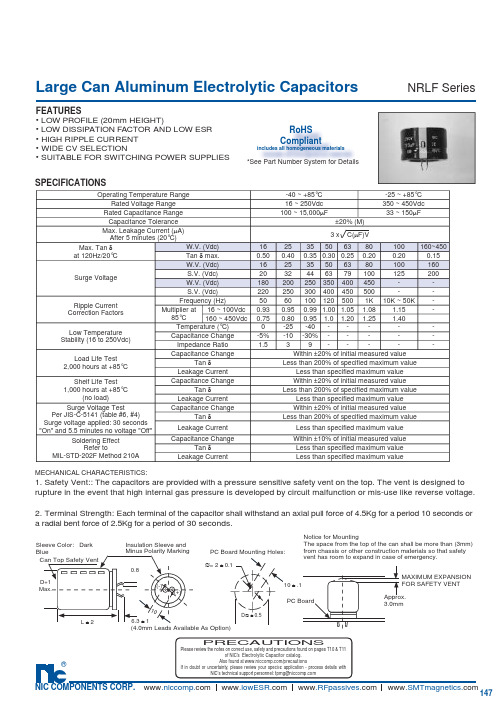
147®NIC COMPONENTS CORP. www www www www Large Can Aluminum Electrolytic CapacitorsFEATURES• LOW PROFILE (20mm HEIGHT)• LOW DISSIPATION FACTOR AND LOW ESR • HIGH RIPPLE CURRENT • WIDE CV SELECTION• SUITABLE FOR SWITCHING POWER SUPPLIES NRLF SeriesSPECIFICATIONSMECHANICAL CHARACTERISTICS:1. Safety Vent:: The capacitors are provided with a pressure sensitive safety vent on the top. The vent is designed torupture in the event that high internal gas pressure is developed by circuit mal f unc t ion or mis-use like reverse voltage.2. Terminal Strength: Each terminal of the capacitor shall withstand an axial pull force of 4.5Kg for a period 10 seconds or a radial bent force of 2.5Kg for a period of 30 seconds.Notice for MountingThe space from the top of the can shall be more than (3mm) from chassis or other construction materials so that safety vent has room to expand in case of emer g en c y.Sleeve Color: Dark BlueCan Top Safety VentInsulation Sleeve and Minus Polarity Marking(4.0mm Leads Available As Option)D+1Max.L ± 26.3 ± 10.810(-)(+)MAXIMUM EX P AN S IONFOR SAFETY VENT Approx. 3.0mmPC Board Mounting Holes:10 ± .1∅= 2 ± 0.1D ∅ ± 0.5PC BoardOperating Temperature Range-40 ~ +85°C-25 ~ +85°C Rated Voltage Range 16 ~ 250Vdc 350 ~ 450Vdc Rated Capacitance Range 100 ~ 15,000µF33 ~ 150µFCapacitance Tolerance ±20% (M)Max. Leakage Current (µA)After 5 minutes (20°C)3 x C(µF)VMax. Tan δat 120Hz/20°C W.V. (Vdc)162535506380100160~450Tan δ max.0.500.400.350.300.250.200.200.15Surge VoltageW.V. (Vdc)162535506380100160S.V. (Vdc)2032446379100125200W.V. (Vdc)180200250350400450--S.V. (Vdc)220250300400450500--Ripple CurrentCorrection FactorsFrequency (Hz)50601001205001K 10K ~ 50K -Multiplier at 85°C 16 ~ 100Vdc 0.930.950.99 1.00 1.05 1.08 1.15-160 ~ 450Vdc 0.750.800.95 1.0 1.20 1.25 1.40Low TemperatureStability (16 to 250Vdc)Temperature (°C)0-25-40-----Capacitance Change-5%-10-30%-----Impedance Ratio 1.539-----Load Life Test2,000 hours at +85°CCapacitance ChangeWithin ±20% of initial measured value Tan δLess than 200% of specifi ed maximum valueLeakage Current Less than specifi ed maximum value Shelf Life Test1,000 hours at +85°C (no load)Capacitance Change Within ±20% of initial measured value Tan δLess than 200% of specifi ed maximum valueLeakage Current Less than specifi ed maximum value Surge Voltage Test Per JIS-C-5141 (table #6, #4)Surge voltage applied: 30 seconds"On" and 5.5 minutes no voltage "Off"Capacitance Change Within ±20% of initial measured value Tan δLess than 200% of specifi ed maximum valueLeakage Current Less than specifi ed maximum value Soldering EffectRefer to MIL-STD-202F Method 210A Capacitance Change Within ±10% of initial measured valueTan δLess than specifi ed maximum value Leakage Current Less than specifi ed maximum valuePRECAUTIONSPlease review the notes on correct use, safety and precautions found on pages T10 & T11of NIC’s Electrolytic Capacitor catalog . Also found at /precautionsIf in doubt or uncertainty, please review your speci fi c application - process details withNIC’s technical support personnel: tpmg@RoHS Compliantincludes all homogeneous materials*See Part Number System for Details148Large Can Aluminum Electrolytic CapacitorsNRLF SeriesNRLF 152 M 50V 22X20 FRoHS compliant Case Size (mm) Voltage Rating Tolerance Code Capacitance Code SeriesPART NUMBER SYSTEM。
THK圆弧导轨
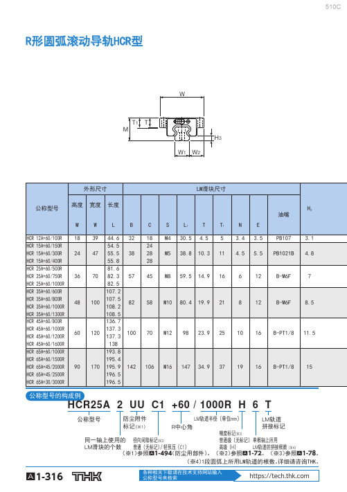
A
〃ީс䖳䈭൞ᢶᵥ᭥ᤷ㖇ㄏ䗉ޛ ޢ〦ශਭᶛỶ㍘
510C
n1- φ d1贯通 φ d2衬孔深度h
θ
LM滚动导轨
θ θ
LM轨道尺寸 宽度 R 100 150 300 400 500 750 1000 600 800 1000 1300 800 1000 1200 1600 1000 1500 2000 2500 3000 R0 106 157.5 307.5 407.5 511.5 761.5 1011.5 617 817 1017 1317 822.5 1022.5 1222.5 1622.5 1031.5 1531.5 2031.5 2531.5 3031.5 Ri 94 142.5 292.5 392.5 488.5 738.5 988.5 583 783 983 1283 777.5 977.5 1177.5 1577.5 968.5 1468.5 1968.5 2468.5 2968.5 L0 100 150 300 400 500 750 1000 600 800 1000 1300 800 1000 1200 1600 1000 1500 1531 1913 1553 U 13.4 20.1 40 54 67 100 134 80 107 134 174 107 134 161 214 134 201 152 190 102 W1 W2 高度 M1 d1×d2×h n1 1 2 60 60 7 7 6 3 2 2.5 2 3 2.5 2.5 2 2 3 2.5 2 2 3 0.5 1.5 1.5 23 23 12 9 7 5 4 9 5.5 5 3.5 8 6 5 4 8 6 4 3.5 3
57
M8
59.5
14.9
16
罗姆ROHM电阻规格书

Quantity / Reel
− − YZP MZP PZPI
15,000 40,000 15,000 10,000
MCR004
0402
01005 RZP
MCR006
0603
0201
YRT MRT
MCR01
1005
0402
(*For further information on datasheet, please refer to AUTOMOTIVE datasheet.)
0.2±0.02 0.3±0.03 0.5±0.05 0.8±0.1 1.25±0.1 1.55±0.15 2.5±0.15 2.5±0.15 3.2±0.15
0.13±0.02 0.23±0.03 0.35±0.05 0.45±0.1 0.5±0.1 0.55±0.1 0.55±0.15 0.55±0.15 0.55±0.15
Size Part No. (mm) (inch)
Type Code GENERAL PURPOSE YZP
AUTOMOTIVE ∗Corresponds to AEC−Q200
Packing Specification Paper tape (2mm pitch) Embossed tape (1mm pitch) Paper tape (2mm pitch)
0.1±0.03 0.15±0.05 0.2±0.1 0.3±0.2 0.35±0.2 0.45±0.25 0.5±0.25 0.6±0.25 0.6±0.25
0.1±0.03 0.15±0.05 0.25 +0.05 −0.1 0.3±0.2 0.35±0.2 0.35±0.25 0.5±0.25 0.6±0.25 0.6±0.25
385B25中文资料
PACKAGING INFORMATIONOrderable Device Status(1)PackageType PackageDrawingPins PackageQtyEco Plan(2)Lead/Ball Finish MSL Peak Temp(3)LM285D-2-5ACTIVE SOIC D875Green(RoHS&no Sb/Br)CU NIPDAU Level-1-260C-UNLIMLM285DE4-2-5ACTIVE SOIC D875Green(RoHS&no Sb/Br)CU NIPDAU Level-1-260C-UNLIMLM285DG4-2-5ACTIVE SOIC D875Green(RoHS&no Sb/Br)CU NIPDAU Level-1-260C-UNLIMLM285DR-2-5ACTIVE SOIC D82500Green(RoHS&no Sb/Br)CU NIPDAU Level-1-260C-UNLIMLM285DRE4-2-5ACTIVE SOIC D82500Green(RoHS&no Sb/Br)CU NIPDAU Level-1-260C-UNLIMLM285DRG4-2-5ACTIVE SOIC D82500Green(RoHS&no Sb/Br)CU NIPDAU Level-1-260C-UNLIMLM285LP-2-5ACTIVE TO-92LP31000Pb-Free(RoHS)CU SN N/A for Pkg TypeLM285LPE3-2-5ACTIVE TO-92LP31000Pb-Free(RoHS)CU SN N/A for Pkg TypeLM285LPR-2-5ACTIVE TO-92LP32000Pb-Free(RoHS)CU SN N/A for Pkg TypeLM285LPRE3-2-5ACTIVE TO-92LP32000Pb-Free(RoHS)CU SN N/A for Pkg TypeLM385BD-2-5ACTIVE SOIC D875Green(RoHS&no Sb/Br)CU NIPDAU Level-1-260C-UNLIMLM385BDE4-2-5ACTIVE SOIC D875Green(RoHS&no Sb/Br)CU NIPDAU Level-1-260C-UNLIMLM385BDG4-2-5ACTIVE SOIC D875Green(RoHS&no Sb/Br)CU NIPDAU Level-1-260C-UNLIMLM385BDR-2-5ACTIVE SOIC D82500Green(RoHS&no Sb/Br)CU NIPDAU Level-1-260C-UNLIMLM385BDRE4-2-5ACTIVE SOIC D82500Green(RoHS&no Sb/Br)CU NIPDAU Level-1-260C-UNLIMLM385BDRG4-2-5ACTIVE SOIC D82500Green(RoHS&no Sb/Br)CU NIPDAU Level-1-260C-UNLIMLM385BLP-2-5ACTIVE TO-92LP31000Pb-Free(RoHS)CU SN N/A for Pkg TypeLM385BLPE3-2-5ACTIVE TO-92LP31000Pb-Free(RoHS)CU SN N/A for Pkg TypeLM385BLPR-2-5ACTIVE TO-92LP32000Pb-Free(RoHS)CU SN N/A for Pkg TypeLM385BLPRE3-2-5ACTIVE TO-92LP32000Pb-Free(RoHS)CU SN N/A for Pkg TypeLM385BPW-2-5ACTIVE TSSOP PW8150Green(RoHS&no Sb/Br)CU NIPDAU Level-1-260C-UNLIMLM385BPWE4-2-5ACTIVE TSSOP PW8150Green(RoHS&no Sb/Br)CU NIPDAU Level-1-260C-UNLIMLM385BPWG4-2-5ACTIVE TSSOP PW8150Green(RoHS&no Sb/Br)CU NIPDAU Level-1-260C-UNLIMLM385BPWR-2-5ACTIVE TSSOP PW82000Green(RoHS&no Sb/Br)CU NIPDAU Level-1-260C-UNLIMLM385BPWRE4-2-5ACTIVE TSSOP PW82000Green(RoHS&no Sb/Br)CU NIPDAU Level-1-260C-UNLIMOrderable Device Status(1)PackageType PackageDrawingPins PackageQtyEco Plan(2)Lead/Ball Finish MSL Peak Temp(3)LM385BPWRG4-2-5ACTIVE TSSOP PW82000Green(RoHS&no Sb/Br)CU NIPDAU Level-1-260C-UNLIMLM385D-2-5ACTIVE SOIC D875Green(RoHS&no Sb/Br)CU NIPDAU Level-1-260C-UNLIMLM385DE4-2-5ACTIVE SOIC D875Green(RoHS&no Sb/Br)CU NIPDAU Level-1-260C-UNLIMLM385DG4-2-5ACTIVE SOIC D875Green(RoHS&no Sb/Br)CU NIPDAU Level-1-260C-UNLIMLM385DR-2-5ACTIVE SOIC D82500Green(RoHS&no Sb/Br)CU NIPDAU Level-1-260C-UNLIMLM385DRE4-2-5ACTIVE SOIC D82500Green(RoHS&no Sb/Br)CU NIPDAU Level-1-260C-UNLIMLM385DRG4-2-5ACTIVE SOIC D82500Green(RoHS&no Sb/Br)CU NIPDAU Level-1-260C-UNLIMLM385LP-2-5ACTIVE TO-92LP31000Pb-Free(RoHS)CU SN N/A for Pkg TypeLM385LPE3-2-5ACTIVE TO-92LP31000Pb-Free(RoHS)CU SN N/A for Pkg TypeLM385LPR-2-5ACTIVE TO-92LP32000Pb-Free(RoHS)CU SN N/A for Pkg TypeLM385LPRE3-2-5ACTIVE TO-92LP32000Pb-Free(RoHS)CU SN N/A for Pkg TypeLM385PW-2-5ACTIVE TSSOP PW8150Green(RoHS&no Sb/Br)CU NIPDAU Level-1-260C-UNLIMLM385PWE4-2-5ACTIVE TSSOP PW8150Green(RoHS&no Sb/Br)CU NIPDAU Level-1-260C-UNLIMLM385PWG4-2-5ACTIVE TSSOP PW8150Green(RoHS&no Sb/Br)CU NIPDAU Level-1-260C-UNLIMLM385PWR-2-5ACTIVE TSSOP PW82000Green(RoHS&no Sb/Br)CU NIPDAU Level-1-260C-UNLIMLM385PWRE4-2-5ACTIVE TSSOP PW82000Green(RoHS&no Sb/Br)CU NIPDAU Level-1-260C-UNLIMLM385PWRG4-2-5ACTIVE TSSOP PW82000Green(RoHS&no Sb/Br)CU NIPDAU Level-1-260C-UNLIM(1)The marketing status values are defined as follows:ACTIVE:Product device recommended for new designs.LIFEBUY:TI has announced that the device will be discontinued,and a lifetime-buy period is in effect.NRND:Not recommended for new designs.Device is in production to support existing customers,but TI does not recommend using this part in a new design.PREVIEW:Device has been announced but is not in production.Samples may or may not be available.OBSOLETE:TI has discontinued the production of the device.(2)Eco Plan-The planned eco-friendly classification:Pb-Free(RoHS),Pb-Free(RoHS Exempt),or Green(RoHS&no Sb/Br)-please check /productcontent for the latest availability information and additional product content details.TBD:The Pb-Free/Green conversion plan has not been defined.Pb-Free(RoHS):TI's terms"Lead-Free"or"Pb-Free"mean semiconductor products that are compatible with the current RoHS requirements for all6substances,including the requirement that lead not exceed0.1%by weight in homogeneous materials.Where designed to be soldered at high temperatures,TI Pb-Free products are suitable for use in specified lead-free processes.Pb-Free(RoHS Exempt):This component has a RoHS exemption for either1)lead-based flip-chip solder bumps used between the die and package,or2)lead-based die adhesive used between the die and leadframe.The component is otherwise considered Pb-Free(RoHS compatible)as defined above.Green(RoHS&no Sb/Br):TI defines"Green"to mean Pb-Free(RoHS compatible),and free of Bromine(Br)and Antimony(Sb)based flame retardants(Br or Sb do not exceed0.1%by weight in homogeneous material)(3)MSL,Peak Temp.--The Moisture Sensitivity Level rating according to the JEDEC industry standard classifications,and peak solder temperature.Important Information and Disclaimer:The information provided on this page represents TI's knowledge and belief as of the date that it is provided.TI bases its knowledge and belief on information provided by third parties,and makes no representation or warranty as to the accuracy of such information.Efforts are underway to better integrate information from third parties.TI has taken and continues to take reasonable steps to provide representative and accurate information but may not have conducted destructive testing or chemical analysis on incoming materials and chemicals.TI and TI suppliers consider certain information to be proprietary,and thus CAS numbers and other limited information may not be available for release.In no event shall TI's liability arising out of such information exceed the total purchase price of the TI part(s)at issue in this document sold by TI to Customer on an annual basis.TAPE AND REEL INFORMATION*All dimensions are nominal Device Package Type Package DrawingPinsSPQ Reel Diameter (mm)Reel Width W1(mm)A0(mm)B0(mm)K0(mm)P1(mm)W (mm)Pin1Quadrant LM285DR-2-5SOICD 82500330.012.4 6.4 5.2 2.18.012.0Q1LM385BDR-2-5SOICD 82500330.012.4 6.4 5.2 2.18.012.0Q1LM385BPWR-2-5TSSOPPW 82000330.012.47.0 3.6 1.68.012.0Q1LM385DR-2-5SOICD 82500330.012.4 6.4 5.2 2.18.012.0Q1LM385PWR-2-5TSSOP PW 82000330.012.47.0 3.6 1.68.012.0Q1*All dimensions are nominalDevice Package Type Package Drawing Pins SPQ Length(mm)Width(mm)Height(mm) LM285DR-2-5SOIC D8*******.5338.120.6 LM385BDR-2-5SOIC D8*******.5338.120.6 LM385BPWR-2-5TSSOP PW82000346.0346.029.0 LM385DR-2-5SOIC D8*******.5338.120.6 LM385PWR-2-5TSSOP PW82000346.0346.029.0IMPORTANT NOTICETexas Instruments Incorporated and its subsidiaries(TI)reserve the right to make corrections,modifications,enhancements,improvements, and other changes to its products and services at any time and to discontinue any product or service without notice.Customers should obtain the latest relevant information before placing orders and should verify that such information is current and complete.All products are sold subject to TI’s terms and conditions of sale supplied at the time of order acknowledgment.TI warrants performance of its hardware products to the specifications applicable at the time of sale in accordance with TI’s standard warranty.Testing and other quality control techniques are used to the extent TI deems necessary to support this warranty.Except where mandated by government requirements,testing of all parameters of each product is not necessarily performed.TI assumes no liability for applications assistance or customer product design.Customers are responsible for their products and applications using TI components.To minimize the risks associated with customer products and applications,customers should provide adequate design and operating safeguards.TI does not warrant or represent that any license,either express or implied,is granted under any TI patent right,copyright,mask work right, or other TI intellectual property right relating to any combination,machine,or process in which TI products or services are rmation published by TI regarding third-party products or services does not constitute a license from TI to use such products or services or a warranty or endorsement e of such information may require a license from a third party under the patents or other intellectual property of the third party,or a license from TI under the patents or other intellectual property of TI.Reproduction of TI information in TI data books or data sheets is permissible only if reproduction is without alteration and is accompanied by all associated warranties,conditions,limitations,and notices.Reproduction of this information with alteration is an unfair and deceptive business practice.TI is not responsible or liable for such altered rmation of third parties may be subject to additional restrictions.Resale of TI products or services with statements different from or beyond the parameters stated by TI for that product or service voids all express and any implied warranties for the associated TI product or service and is an unfair and deceptive business practice.TI is not responsible or liable for any such statements.TI products are not authorized for use in safety-critical applications(such as life support)where a failure of the TI product would reasonably be expected to cause severe personal injury or death,unless officers of the parties have executed an agreement specifically governing such use.Buyers represent that they have all necessary expertise in the safety and regulatory ramifications of their applications,and acknowledge and agree that they are solely responsible for all legal,regulatory and safety-related requirements concerning their products and any use of TI products in such safety-critical applications,notwithstanding any applications-related information or support that may be provided by TI.Further,Buyers must fully indemnify TI and its representatives against any damages arising out of the use of TI products in such safety-critical applications.TI products are neither designed nor intended for use in military/aerospace applications or environments unless the TI products are specifically designated by TI as military-grade or"enhanced plastic."Only products designated by TI as military-grade meet military specifications.Buyers acknowledge and agree that any such use of TI products which TI has not designated as military-grade is solely at the Buyer's risk,and that they are solely responsible for compliance with all legal and regulatory requirements in connection with such use. TI products are neither designed nor intended for use in automotive applications or environments unless the specific TI products are designated by TI as compliant with ISO/TS16949requirements.Buyers acknowledge and agree that,if they use any non-designated products in automotive applications,TI will not be responsible for any failure to meet such requirements.Following are URLs where you can obtain information on other Texas Instruments products and application solutions:Products ApplicationsAmplifiers AudioData Converters AutomotiveDSP BroadbandClocks and Timers Digital ControlInterface MedicalLogic MilitaryPower Mgmt Optical NetworkingMicrocontrollers SecurityRFID TelephonyRF/IF and ZigBee®Solutions Video&ImagingWirelessMailing Address:Texas Instruments,Post Office Box655303,Dallas,Texas75265Copyright©2008,Texas Instruments Incorporated。
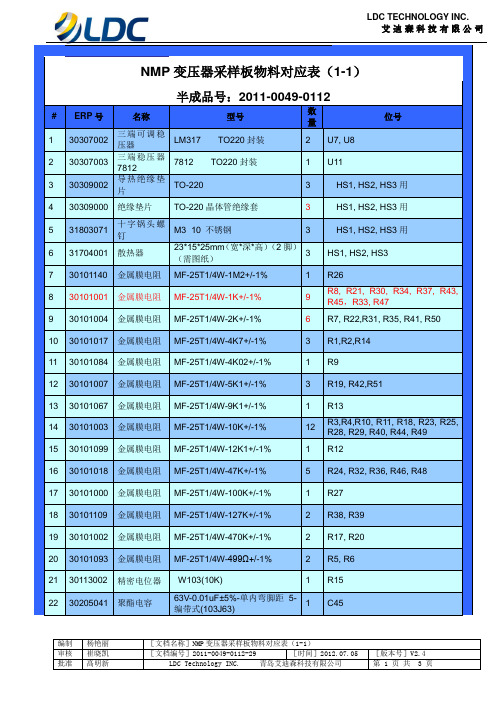
NMP变压器采样板物料对应表(1-1)V2.4
D6, D7, D8, D11, D12, D28, D29,ቤተ መጻሕፍቲ ባይዱD31, D32, D39
30
30301000
二极管
1000V-1A-DO41-编带式(1N4007)
10
D13, D14, D16, D17, D19, D20, D21, D22, D41, D43
31
30301003
二极管
100V-0.1A-DO35-编带式(1N4148)
17
C1, C2, C3, C4, C5, C25, C27, C32, C34, C36, C38, C40, C41, C47, C48, C49, C50
24
30202051
铝电解电容
50V-470uF-12*20(-25℃~+105℃)
1
C29
25
30202045
铝电解电容
50V-2.2uF-5*11(-25℃~+105℃)
4针白色插座3.96MM
2
CN2, CN13
45
30906009
单列接插件
3针白色插座3.96MM
4
CN1,CN4,CN11,CN12
46
30906012
单列接插件
2针白色插座3.96MM(小)
2
CN15,CN16
47
30906022
单列接插件
9针白色插座2.54MM(短针)
1
CN10
48
30906048
38
30501090
工频变压器
EI48(卧式)220/18V 220V/12.7V*2
3
T1, T2, T3
39
LM3905资料
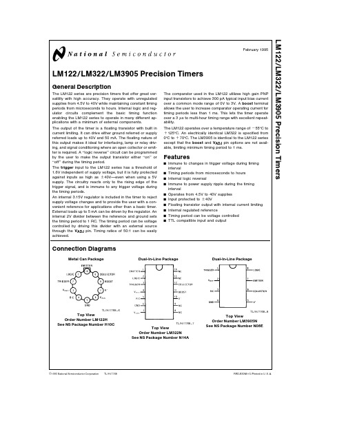
TL H 7768LM122 LM322 LM3905Precision TimersFebruary 1995LM122 LM322 LM3905Precision TimersGeneral DescriptionThe LM122series are precision timers that offer great ver-satility with high accuracy They operate with unregulated supplies from 4 5V to 40V while maintaining constant timing periods from microseconds to hours Internal logic and reg-ulator circuits complement the basic timing function enabling the LM122series to operate in many different ap-plications with a minimum of external componentsThe output of the timer is a floating transistor with built in current limiting It can drive either ground referred or supply referred loads up to 40V and 50mA The floating nature of this output makes it ideal for interfacing lamp or relay driv-ing and signal conditioning where an open collector or emit-ter is required A ‘‘logic reverse’’circuit can be programmed by the user to make the output transistor either ‘‘on’’or ‘‘off’’during the timing periodThe trigger input to the LM122series has a threshold of 1 6V independent of supply voltage but it is fully protected against inputs as high as g 40V even when using a 5V supply The circuitry reacts only to the rising edge of the trigger signal and is immune to any trigger voltage during the timing periodsAn internal 3 15V regulator is included in the timer to reject supply voltage changes and to provide the user with a con-venient reference for applications other than a basic timer External loads up to 5mA can be driven by the regulator An internal 2V divider between the reference and ground sets the timing period to 1RC The timing period can be voltage controlled by driving this divider with an external source through the V ADJ pin Timing ratios of 50 1can be easily achievedThe comparator used in the LM122utilizes high gain PNP input transistors to achieve 300pA typical input bias current over a common mode range of 0V to 3V A boost terminal allows the user to increase comparator operating current for timing periods less than 1ms This lets the timer operate over a 3m s to multi-hour timing range with excellent repeat-abilityThe LM122operates over a temperature range of b 55 C to a 125 C An electrically identical LM322is specified from 0 C to a 70 C The LM3905is identical to the LM122series except that the boost and V ADJ pin options are not avail-able limiting minimum timing period to 1msFeaturesY Immune to changes in trigger voltage during timing intervalY Timing periods from microseconds to hours Y Internal logic reversalYImmune to power supply ripple during the timing intervalY Operates from 4 5V to 40V supplies Y Input protected to g 40VY Floating transistor output with internal current limiting Y Internal regulated referenceY Timing period can be voltage controlled YTTL compatible input and outputConnection DiagramsMetal Can PackageTL H 7768–6Top ViewOrder Number LM122H See NS Package Number H10CDual-In-Line PackageTL H 7768–7Top ViewOrder Number LM322N See NS Package Number N14ADual-In-Line PackageTL H 7768–8Top ViewOrder Number LM3905N See NS Package Number N08EC 1995National Semiconductor Corporation RRD-B30M115 Printed in U S AAbsolute Maximum RatingsIf Military Aerospace specified devices are required please contact the National Semiconductor Sales Office Distributors for availability and specifications Power Dissipation500mW V a Voltage40V Collector Output Voltage40V V REF Current5mA Trigger Voltage g40V V ADJ Voltage(Forced)5V Logic Reverse Voltage5 5V Output Short Circuit Duration(Note1)Lead Temperature(Soldering 10sec )260 C Operating Temperature RangeLM122b55 C s T A s a125 C LM3220 C s T A s a70 C LM39050 C s T A s a70 CElectrical Characteristics(Note2)Parameter ConditionsLM122LM322LM3905Units Min Typ Max Min Typ Max Min Typ MaxTiming Ratio T A e25 C 4 5V s V a s40V0 6260 6320 6380 6200 6320 6440 6200 6320 644 Boost Tied to V a (Note3)0 6200 6320 6440 6200 6320 644Comparator Input T A e25 C 4 5V s V a s40V0 31 00 31 50 51 5nA Current Boost Tied to V a3010030100nA Trigger Voltage T A e25 C 4 5V s V a s40V1 21 621 21 621 21 62VTrigger Current T A e25 C V TRIG e2V252525m A Supply Current T A t25 C 4 5V s V a s40V2 542 54 52 54 5mATiming Ratio4 5V s V a s40V0 620 6440 610 6540 610 654 Boost Tied to V a0 620 6440 610 654Comparator Input4 5V s V a s40V b55b22b2 52 5nA Current Boost Tied to V a (Note4)100150nATrigger Voltage4 5V s V a s40V0 82 50 82 50 82 5V Trigger Current V TRIG e2 5V200200200m A Output Leakage V CE e40V155m A CurrentCapacitor Saturation R t t1M X2 52 52 5mV Voltage R t e10k X252525mV Reset Resistance150150150X Reference Voltage T A e25 C33 153 333 153 333 153 3V Reference Regulation0s I OUT s3mA205020502050mV4 5V s V a s40V625625625mV Collector Saturation I L e8mA0 250 40 250 40 250 4V Voltage I L e50mA0 71 40 71 40 71 4V Emitter Saturation T A e25 C I L e3mA1 82 21 82 21 82 2V Voltage T A e25 C I L e50mA2 132 132 13V Average TemperatureCoefficient of Timing0 0030 0030 003% C RatioMinimum Trigger Width V TRIG e3V0 250 250 25m s Note1 Continuous output shorts are not allowed Short circuit duration at ambient temperatures up to40 C may be calculated from t e120 V CE seconds where V CE is the collector to emitter voltage across the output transistor during the shortNote2 These specifications apply for T AMIN s T A s T AMAX unless otherwise notedNote3 Output pulse width can be calculated from the following equation t e(R t)(C t) 1b2(0 632b r)b V C V REF)where r is timing ratio and V C is capacitor saturation voltage This reduces to t e(R t)(C t)for all but the most critical applicationsNote4 Sign reversal may occur at high temperatures(l100 C)where comparator input current is predominately leakage See typcial curvesNote5 Refer to RETS122X drawing of military LM122H version for specifications2Typical Performance CharacteristicsComparator Bias CurrentComparator Bias Current(LM122 LM322)Comparator Bias Current TL H 7768–3Supply Current Trigger Input Characteristics Trigger ThresholdCharacteristics at Low Currents Output Transistor Saturation Characteristics at High Current Collector Output Saturation Comparator Bias CurrentTiming Error Due toReference Regulation Reference Regulation Suggested Timing Components(LM122 LM322)Short Output Pulse (LM122 LM322)Short Output Pulse Logic Pin CharacteristicsTL H 7768–43Schematic DiagramT L H 7768–54Functional DiagramTL H 7768–9 Timing DiagramTL H 7768–10 Pin Function DescriptionOne of the main features of the LM122is its great versatility Since this device is unique a description of the functions and limitations of each pin is in order This will make it much easier to follow the discussion of the various applications presented in this noteV a is the positive supply terminal of the LM122 When us-ing a single supply this terminal may be driven by any volt-age between4 5V and40V The effect of supply variations on timing period is less than0 005% V so supplies with high ripple content may be used without causing pulse width changes Supply bypassing on V a is not generally needed but may be necessary when driving highly reactive loadsQuiescent current drawn from the V a terminal is typically2 5mA independent of the supply voltage Of course addi-tional current will be drawn if the reference is externally loadedThe V REF pin is the output of a3 15V series regulator refer-enced to the ground pin Up to5 0mA can be drawn from this pin for driving external networks In most applications the timing resistor is tied to V REF but it need not be in situations where a more linear charging current is required The regulated voltage is very useful in applications where the LM122is not used as a timer such as switching regula-tors variable reference comparators and temperature con-5Pin Function Description(Continued)trollers Typical temperature drift of the reference is less than0 01% CThe trigger terminal is used to start a timing cycle(see functional diagram) Initially Q1is saturated C t is dis-charged and the latching buffer output(V1)is latched high A trigger pulse unlatches the buffer V1goes low and turns Q1off The timing capacitor C t connected from R C to GND will begin to charge When the voltage at the R C terminal reaches the2 0V threshold of the comparator the compara-tor toggles latching the buffer output(V1)in the high state This turns on Q1 discharges the capacitor C t and the cycle is ready to begin againIf the trigger is held high as the timing period ends the comparator will toggle and V1will go high exactly as before However V1will not be latched and the capacitor will not discharge until the trigger again goes low When the trigger goes low V1remains high but is now latchedTrigger threshold is typically1 6V at25 C and has a tem-perature dependence of b5 0mV C Current drawn from the trigger source is typically20m A at threshold rising to 600m A at30V then leveling off due to FET action of the series resistor R5 For negative input trigger voltages the only current drawn is leakage in the nA region The trigger can be driven from supplies as high as g40V even when device supply voltage is only5VThe R C pin is tied to the non-inverting side of the compara-tor and to the collector of Q1 Timing ends when the voltage on this pin reaches2 0V(1RC time constant referenced to the3 15V regulator) Q1turns on only if the trigger voltage has dropped below threshold In comparator or regulator applications of the timer the trigger is held permanently high and the R C pin acts just like the input to an ordinary comparator The maximum voltages which can be applied to this pin are a5 5V and b0 7V Current from the R C pin is typically300pA when the voltage is negative with respect to the V ADJ terminal For higher voltages the current drops to leakage levels In the boosted mode input current is typical-ly30nA Gain of the comparator is very high 200 000or more depending on the state of the logic reverse pin and the connection of the output transistorThe ground pin of the LM122need not necessarily be tied to system ground It can be connected to any positive or negative voltage as long as the supply is negative with re-spect to the V a terminal Level shifting may be necessary for the input trigger if the trigger voltage is referred to sys-tem ground This can be done by capacitive coupling or by actual resistive or active level shifting One point must be kept in mind the emitter output must not be held above the ground terminal with a low source impedance This could occur for instance if the emitter were grounded when the ground pin of the LM122was tied to a negative supply The terminal labled V ADJ is tied to one side of the compara-tor and to a voltage divider between V REF and ground The divider voltage is set at63 2%of V REF with respect to ground exactly one RC time constant The impedance of the divider is increased to about30k with a series resistor topresent a minimum load on external signals tied to V ADJThis resistor is a pinched type with a typical variation innominal value of b50% a100%and a TC of0 7% C For this reason external signals(typically a pot between V REFand ground)connected to V ADJ should have a source re-sistance as low as possible For small changes in V ADJ upto several k X is all right but for large variations 250X orless should be maintained This can be accomplished with a1k pot since the maximum impedance from the wiper is250X If a voltage is forced on V ADJ from a hard sourcevoltage should be limited to b0 5 and a5 0V or currentlimited to g1 0mA This includes capacitively coupled sig-nals because even small values of capacitors containenough energy to degrade the input stage if the capacitor isdriven with a large fast slewing signal The V ADJ pin may beused to abort the timing cycle Grounding this pin during thetiming period causes the timer to react just as if the capaci-tor voltage had reached its normal RC trigger point thecapacitor discharges and the output charges state An ex-ception to this occurs if the trigger pin is held high when theV ADJ pin is grounded In this case the output changesstate but the capacitor does not dischargeIf the trigger drops while V ADJ is being held low dischargewill occur immediately and the cycle will be over If the trig-ger is still high when V ADJ is released the output may ormay not change state depending on the voltage across thetiming capacitor For voltages below2 0V across the timingcapacitor the output will change state immediately thenonce more as the voltage rises past2 0V For voltagesabove2 0V no change will occur in the output This pin isnot available on the LM2905 LM3905In noisy environments or in comparator-type applications abypass capacitor on the V ADJ terminal may be needed toeliminate spurious outputs because it is high impedancepoint The size of the cap will depend on the frequency andenergy content of the noise A0 1m F will generally sufficefor spike suppression but several m F may be used if thetimer is subjected to high level60Hz EMIThe emitter and the collector outputs of the timer can betreated just as if they were an ordinary transistor with40Vminimum collector-emitter breakdown voltage Normally theemitter is tied to the ground pin and the signal is taken from the collector or the collector is tied to V a and the signal is taken from the emitter Variations on these basic connections are possible The collector can be tied to any positive voltage up to40V when the signal is taken from the emitter However the emitter will not be pulled higher than the supply voltage on the V a pin Connecting the collector to a voltage less than the V a voltage is allowed The emit-ter should not be connected to a low impedance load other than that to which the ground pin is tied The transistor has built-in current limiting with a typical knee current of120mA Temporary short circuits are allowed even with collector-emitter voltages up to40V The power x time product how-ever must not exceed15watt-seconds for power levels above the maximum rating of the package A short to30V6Pin Function Description(Continued)for instance cannot be held for more than4seconds These levels are based on40 C maximum initial chip tem-perature When driving inductive loads always use a clamp diode to protect the transistor from inductive kick-backA boost pin is provided on the LM122to increase the speed of the internal comparator The comparator is normally op-erated at low current levels for lowest possible input current For timing periods less than1ms where low input current is not needed comparator operating current can be increased several orders of magnitude Shorting the boost terminal to V a increases the emitter current of the vertical PNP drivers in the differential stage from25nA to5m A This pin is notavailable on the LM3905With the timer in the unboosted state timing periods are accurate down to about1ms In the boosted mode loss of accuracy due to comparator speed is only about800ns so timing periods of several microseconds can be used The 800ns error is relatively insensitive to temperature so tem-perature coefficient of pulse width is still goodThe Logic pin is used to reverse the signal appearing at the output transistor An open or‘‘high’’condition on the logic pin programs the output transistor to be‘‘off’’during the timing period and‘‘on’’all other times Grounding the logic pin reverses the sequence to make the transistor‘‘on’’dur-ing the timing period Threshold for the logic pin is typically 100mV with150m A flowing out of the terminal If an active drive to the logic pin is desired a saturated transistor drive is recommended either with a discrete transistor or the open collector output of integrated logic A maximum V SAT of25mV at200m A is required Minimum and maximum voltages that may appear on the logic pin are0and a5 0 respectivelyTypical ApplicationsBasic TimersFigure1is a basic timer using the collector output R t and C t set the time interval with R L as the load During the timing interval the output may be either high or low depending on the connection of the logic pin Timing waveforms are shown in the sketch along side Figure1 Note that the trig-ger pulse may be either shorter or longer than the output pulse widthFigure2is again a basic timer but with the output taken from the emitter of the output transistor As with the collec-tor output either a high or low condition may be obtained during the timing periodSimulating a Thermal Delay RelayFigure3is an application where the LM122is used to simu-late a thermal delay relay which prevents power from being applied to other circuitry until the supply has been on for some time The relay remains de-energized for R t C t sec-onds after V CC is applied then closes and stays energized until V CC is turned off Figure4is a similar circuit except that the relay is energized as soon as V CC is applied R t C t sec-onds later the relay is de-energized and stays off until the V CC supply is recycledTL H 7768–11FIGURE1 Basic Timer-CollectorOutput and Timing ChartTL H 7768–12 FIGURE2 Basic Timer-Emitter Output and Timing ChartTL H 7768–13FIGURE3 Time Out on Power Up(Relay Energized R t C t Seconds after V CC is Applied)a5V Supply Driving28V RelayFigure5shows the timer interfacing5V logic to a high volt-age relay Although the V a terminal could be tied to the a28V supply this may be an unnecessary waste of power in the IC or require extra wiring if the LM122is on a logic card In either case the threshold for the trigger is1 6V7Typical Applications(Continued)TL H 7768–14 FIGURE4 Time Out on Power Up(Relay Energized Until R t C t Seconds After V CC is Applied)TL H 7768–15 FIGURE5 5V Logic Supply Driving28V Relay30V Supply Interfacing with5V LogicFigure6indicates the ability of the timer to interface to digi-tal logic when operating off a high supply voltage V OUT swings between a5V and ground with a minimum fanout of 5for medium speed TTL If the logic is sensitive to rise fall time of the trailing edge of the output pulse the trigger pin should be low at that timeTL H 7768–16 FIGURE6 30V Supply Interfacing with5V Logic Astable OperationThe LM122can be made into a self-starting oscillator by feeding the output back to the trigger input through a capac-itor as shown in Figure7 Operating frequency is1 (R t a R1)(C t) The output is a narrow negative pulse whose width is approximately2R2C f For optimum frequency stability C f should be as small as possible The minimum value is deter-mined by the time required to discharge C t through the inter-nal discharge transistor A conservative value for C f can be chosen from the graph included with Figure20 For frequen-cies below1kHz the frequency error introduced by C f is a few tenths of one percent or less for R t t500kSee ChartTL H 7768–17TL H 7768–18FIGURE7 OscillatorOne Hour Timer with Reset and Manual Cycle EndFigure8shows the LM122connected as a one hour timer with manual controls for start reset and cycle end S1 starts timing but has no effect after timing has started S2isa center off switch which can either end the cycle prema-turely with the appropriate change in output state and dis-charging of C t or cause C t to be reset to0V without a change in output In the latter case a new timing period starts as soon as S2is releasedDearbornElectronicsLP9A1A476KPolycarbonateTL H 7768–19 FIGURE8 One Hour Timer with Resetand Manual Cycle End8Typical Applications (Continued)The average charging current through R t is about 30nA so some attention must be paid to parts layout to prevent stray leakage paths The suggested timing capacitor has a typical self time constant of 300hours and a guaranteed minimum of 25hours at a 25 C Other capacitor types may be used if sufficient data is available on their leakage characteristics Two Terminal Time Delay SwitchThe LM122can be used as a two terminal time delay switch if an ‘‘on’’voltage drop of 2V to 3V can be tolerated In Figure 9 the timer is used to drive a relay ‘‘on’’R t C t seconds after application of power ‘‘Off’’current of the switch is 4mA maximum and ‘‘on’’current can be as high as 50mAZero Power Dissipation Between Timing IntervalsIn some applications it is desirable to reduce supply current drain to zero between timing cycles In Figure 10this is accomplished by using an external PNP as a latch to drive the V a pin of the timerBetween timing periods Q1is off and no supply current is drawn When a trigger pulse of 5V minimum amplitude is received the LM122output transistor and Q1latch for the duration of the timing period D1prevents the step on the V a pin from coupling back into the trigger pin If the trigger input is a short pulse C1and R2may be eliminated R L must have a minimum value of (V CC ) (2 5mA)TL H 7768–20FIGURE 9 2-Terminal Time Delay SwitchFrequency to Voltage ConverterAn accurate frequency to voltage converter can be made with the LM122by averaging output pulses with a simple one pole filter as shown in Figure 11 Pulse width is adjusted with R2to provide initial calibration at 10kHz The collector of the output transistor is tied to V REF giving constant am-plitude pulses equal to V REF at the emitter output R4and C1filter the pulses to give a dc output equal to (R t )(C t )(V REF )(f) Linearity is about 0 2%for a 0V to 1V out-put If better linearity is desired R5can be tied to the sum-ming node of an op amp which has the filter in the feedback path If a low output impedance is desired a unity gain buff-er such as the LM110can be tied to the output An analog meter can be driven directly by placing it in series with R5to ground A series RC network across the meter to provide damping will improve response at very low frequencies Pulse Width DetectorBy driving the logic terminal of the LM122simultaneous to the trigger input a simple accurate pulse width detector can be made (Figure 12)TL H 7768–21FIGURE 10 Zero Power DissipationBetween Timing IntervalsTL H 7768–22FIGURE 11 Frequency to Voltage Converter(Tachometer)Output Independent of Supply VoltageTL H 7768–23V OUT e 0for W R 1C 1Pulse Out e W b R 1C 1for W R 1C 1FIGURE 12 Pulse Width Detector9Typical Applications(Continued)In this application the logic terminal is normally held high byR3 When a trigger pulse is received Q1is turned on driv-ing the logic terminal to ground The result of triggering thetimer and reversing the logic at the same time is that theoutput does not change from its initial low condition Theonly time the output will change states is when the triggerinput stays high longer than one time period set by R t andC t The output pulse width is equal to the input trigger widthminus R t C t C2insures no output pulse for short(k RC) trigger pulses by prematurely resetting the timing capacitorwhen the trigger pulse drops C L filters the narrow spikeswhich would occur at the output due to propagation delaysduring switching5V Switching RegulatorFigure13is an application where the LM122does not useits timing function A switching regulator is made using theinternal reference and comparator to drive a PNP transistorswitch Features of this circuit include a5 5V minimum inputvoltage at1A output current low part count and good effi-ciency(l75%)for input voltages to10V Line and loadregulation are less than0 5%and output ripple at theswitching frequency is only30mV Q1is an inexpensiveplastic device which does not need a heatsink for ambienttemperature up to50 C D1should be a fast switching di-ode Output voltage can be adjusted between1V and30V by choosing proper values for R2 R3 R4 and R5 For out-puts less than2V a divider with250X Thevinin resistance must be connected between V REF and ground with its tap point tied to V ADJNo 22Wire Wound on Molybdenum Permalloy Core TL H 7768–24 FIGURE13 5V Switching Regulator with1Amp Output and5 5V Minimum InputApplication HintsAborting a Timing CycleThe LM122does not have an input specifically allocated to a stop-timing function If such a function is desired it may be accomplished several waysGround V ADJRaise R C more positive than V ADJWire‘‘OR’’the outputGrounding V ADJ will end the timing cycle just as if the timingcapacitor had reached its normal discharge point A newtiming cycle can be started by the trigger terminal as soonas the ground is released A switching transistor is best fordriving V ADJ to as near ground as possible Worst case sinkcurrent is about300m AA timing cycle may also be ended by a positive pulse to aresistor(R s R t 100)in series with the timing capacitorThe pulse amplitude must be at least equal to V ADJ(2 0V)but should not exceed5 0V When the timing capacitor dis-charges a negative spike of up to2 0V will occur across theresistor so some caution must be used if the drive pulse isused for other circuitryTL H 7768–25FIGURE14 Cycle InterruptThe output of the timer can be wire ORed with a discretetransistor or an open collector logic gate output This allowsoverriding of the timer output but does not cause the timerto be reset until its normal cycle time has elapsedUsing the LM122as a ComparatorA built-in reference and zero volt common mode limit makethe LM122very useful as a comparator Threshold may beadjusted from zero to three volts by driving the V ADJ termi-nal with a divider tied to V REF Stability of the referencevoltage is typically g1%over a temperature range of b55 C to a125 C Offset voltage drift in the comparator is typically25m V C in the boosted mode and50m V C un-boosted A resistor can be inserted in series with the inputto allow overdrives up to g50V as shown in Figure15 There is actually no limit on input voltage as long as current is limited to g1mA The resistor shown contributes a worst case of5mV to initial offset In the unboosted mode the error drops to0 25mV maximum The capability of operat-ing off a single5V supply with internal reference should make this comparator very useful10Application Hints(Continued)Timer ProtectedAgainst Damagefor up to50VTL H 7768–26 FIGURE15 Comparator with0V to3V Threshold Eliminating Timing Cycle Upon InitialApplication of PowerThe LM122will normally start a timing cycle(with no trigger input)when V a is first turned on If this characteristic is undesirable it can be defeated by tying the timing capacitor to V REF instead of ground as shown in Figure16 This con-nection does not affect operation of the timer in any other way If an electrolytic timing capacitor is used be sure the negative end is tied to the R C pin and the positive end to V REF A1 0k X resistor should be included in series with the timing capacitor to limit the surge current load on V REF when the capacitor is dischargedTL H 7768–27 FIGURE16 Eliminating Initial Timing CycleUsing Dual SuppliesThe LM122can be operated off dual supplies as shown in Figure17 The only limitation is that the emitter terminal cannot be tied to ground it must either drive a load referred to V b or be actually tied to V b as shown Although capaci-tive coupling is shown for the trigger input(to allow5V trig-gering) a resistor can be substituted for C1 R2must be chosen to give proper level shifting between the trigger sig-nal and the trigger pin of the timer Worst case‘‘lo’’on the trigger pin(with respect to V b)is0 8V and worst case‘‘high’’is2 5V R2may be calculated from the divider equa-tion with R1to give these levelsTL H 7768–28 Select for Proper Level ShiftEmitter Terminal or Emitter Load must be Tied to GND Pin of TimerFIGURE17 Operating Off Dual Supplies Linearizing the Charging SweepIn some applications(such as a linear pulse width modula-tor)it may be desirable to have the timing capacitor charge from a constant current source A simple way to accomplish this is shown in Figure18TL H 7768–29 FIGURE18 Temperature CompensatedLinear Charging SweepQ1converts the current through R1to a current source in-dependent of the voltage across C t R2 R3 D1 and D2are added to make the current through R1independent of sup-ply variations and temperature changes (D2is a low TC type)D2and R3can be omitted if the V a supply is stable and D1and R2can be omitted also if temperature stability is not critical With D1 D2 R2and R3omitted the current through R1will change about0 015% C with a15V supply and0 1% C with a5 0V supply11。
LM39500中文资料

APPLICATIONS•Low-voltage Digatal Ics•LDO linear regulator for PC add-in cards •High-efficiency linear power supplies •Multimedia and PC processor supplies •SMPS post regulator•Low-voltage microcontrollers •Strong ARM™ processor supplyORDERING INFORMATIONDESCRIPTIONHTCTO-263LM39500-X.X LM39500R- X.X TO-220LM39502T-AdjLM39502-AdjLM39500T-X.X TO-220LM39501T-X.X TO-220ADJOUT Device Marking LM39502R-Adj Logic low or open = Shutdown Supply (Input): +16V maximum supply Flag (Output): Open-collector error flag output.LM39501R-X.X TO-263LM39501-X.X Regulator OutputLM39501-X.X GND FLG Ground pin and TAB are internally connected.LM39500-X.X Adjustment Input: Feedback input.Package LM39502-Adj TO-263PIN DESCRIPTIONEnable (Input)IN CMOS-compatible control input.Logic high = enable, logic * X.X = Fixed Vout = 1.5V, 1.8V, 2.5V, 3.3V, 5.0V The LM39500/1/2 is ideal for PC Add-In cards that need to convert from standard 5V or 3.3V, down to new, lower core voltages. A guaranteed maximum dropout voltage of 500mV over all operating conditions allows the LM39500/1/2 to provide 2.5V from a supply as low as 3V. The LM39500 also has fast transient response, for heavy switching applications. The device requires only 47F of output capacitance to maintain stability and achieve fast transient responseThe LM39500/1/2 is fully protected with overcurrentlimiting,thermal shutdown, reversed-battery and reversed-lead in-sertion protection. The LM39501 offers a TTL-logic-compat-ible enable pin and an error flag that indicates undervoltage and overcurrentconditions. The LM39500/1/2 comes in the TO-220 and TO-263 packages and is an ideal upgrade to older,NPN-based linear voltage regulators.The LM39502 is adjustable version.TO263-3L / TO220-3LTO263-5L / TL220-5L(39501-x.x & 39502 only)The LM39500, LM39501 and LM39502 is a 5A low-dropout linear voltage regulator that provides a low-voltage, high-current output with aminimum of external components. Utilizing Super beta PNP pass element, The LM39500 offers extremely low dropout (typically 400mV at 5A)and low ground current (typically 70mA at 5A).Typical Application CircuitAbsolute Maximum Ratings (Note 1)Supply Voltage (VIN) : –20V to +20V Enable Voltage (VEN) : +20VStorage Temperature (TS) : –65°C to +150°C Lead Temperature (soldering, 5 sec) : 260°C ESD, Note 3Operating Ratings (Note 2)Supply Voltage (VIN) : +2.25V to +16V Enable Voltage (VEN) : +16VMaximum Power Dissipation (PD(max)) Note 4 Junction Temperature (TJ) : –40°C to +125°C Package Thermal Resistance TO-263(θJC ) : 2°C/W TO-220(θJC) : 2°C/WLM39500LM39501LM39502Block DiagramLM39500 Fixed (1.5V,1.8V,2.5V,3.3V,5.0V)LM39501 Fixed with Flag and EnableLM39502 AdjustableNote 1. Exceeding the absolute maximum ratings may damage the device.Note 2. The device is not guaranteed to function outside its operating rating.Note 3. Devices are ESD sensitive. Handling precautions recommended.Note 4. P D(max) = (T J(max) – T A) θJA, where θJA depends upon the printed circuit layout. See “Applications Information.”Note 5.Vout temperature coefficient is ∆V OUT(worst case) (T J(max) – T J(min)) where T J(max) is +125℃ and T J(min) is 0℃Note 6. V DO = V IN – V OUT when V OUT decreases to 98% of its nominal output voltage with V IN = V OUT + 1V.Note 7. I GND is the quiescent current. IIN = I GND + I OUT.Note 8. V EN 0.8V, V IN 8V, and V OUT = 0VNote 9. For a 2.5V device, V IN = 2.250V (device is in dropout).Application InformationThe LM39500/1 is a high-performance low-dropout voltage regulator suitable for moderate to high-current voltage regu-lator applications. Its 400mV dropout voltage at full load makes it especially valuable in battery-powered systems and as a high-efficiency noise filter in post-regulator applications. Unlike older NPN-pass transistor designs, where the mini-mum dropout voltage is limited by the base-to-emitter voltage drop and collector-to-emitter saturation voltage, dropout per-formance of the PNP output of these devices is limited only by the low V CE saturation voltage.A trade-off for the low dropout voltage is a varying base drive requirement.The LM39500/1/2 regulator is fully protected from damage due to fault conditions. Current limiting is provided. This limiting is linear output current during overload conditions is constant. Thermal shutdown disables the device when the die temperature exceeds the maximum safe operating tem-perature. Transient protection allows device (and load) sur-vival even when the input voltage spikes above and below nominal. The output structure of these regulators allows voltages in excess of the desired output voltage to be applied without reverse current flow.Thermal DesignLinear regulators are simple to use. The most complicated design parameters to consider are thermal characteristics.Thermal design requires four application-specific param-eters:•Maximum ambient temperature (T A)•Output Current (I OUT)•Output Voltage (V OUT)•Input Voltage (V IN)•Ground Current (I GND)Calculate the power dissipation of the regulator from these numbers and the device parameters from this datasheet,where the ground current is taken from the data sheet.PD = (V IN – V OUT) I OUT + V IN·I GNDThe heat sink thermal resistance is determined by:θSA=(T JMAX-T A)/P D -(θJC+θCS)where TJ (max) 125 ℃ and θCS is between 0℃ and 2℃/W.The heat sink may be significantly reduced in applications where the minimum input voltage is known and is large compared with the dropout voltage. Use a series input resistor to drop excessive voltage and distribute the heat between this resistor and the regulator. The low dropout properties of Taejin regulators allow signifi-cant reductions in regulator power dissipation and the asso-ciated heat sink without compromising performance. When this technique is employed, a capacitor of at least 1.0F is needed directly between the input and regulator ground.Refer to Application Note 9 for further details and examples on thermal design and heat sink specification.Output CapacitorThe LM39500/1/2 requires an output capacitor to maintain stability and improve transient response. Proper capacitor selection is important to ensure proper operation. The LM39500/1/2 output capacitor selection is dependent upon the ESR (equivalent series resistance) of the output capacitor to maintain stability. When the output capacitor is 47F or greater, the output capacitor should have less than 1 of ESR. This will improve transient response as well as promote stability. Ultralow ESR capacitors, such as ceramic chip capacitors may promote instability. These very low ESR levels may cause an oscillation and/or underdamped tran-sient response. A low-ESR solid tantalum capacitor works extremely well and provides good transient response and stability over temperature. Aluminum electrolytics can also be used, as long as the ESR of the capacitor is < 1.The value of the output capacitor can be increased without limit. Higher capacitance values help to improve transient response and ripple rejection and reduce output noise. Input CapacitorAn input capacitor of 1uF or greater is recommended when the device is more than 4 inches away from the bulk ac supply capacitance, or when the supply is a battery. Small, surface-mount, ceramic chip capacitors can be used for the bypass-ing. Larger values will help to improve ripple rejection by bypassing the input to the regulator, further improving the integrity of the output voltage.Transient Response and 3.3V.Fig 1. Capacitor RequirementsMinimum Load CurrentThe LM39500/1/2 regulator is specified between finite loads.If the output current is too small, leakage currents dominate and the output voltage rises.A 10mA minimum load current is necessary for proper regulation.Transient Response and 3.3V to 2.5V ConversionThe LM39500/1/2 has excellent transient response to varia-tions in input voltage and load current. The device has been designed to respond quickly to load current variations and input voltage variations. Large output capacitors are not required to obtain this performance. A standard 47F output capacitor, preferably tantalum, is all that is required. Larger values help to improve performance even further.By virtue of its low-dropout voltage, this device does not saturate into dropout as readily as similar NPN-based de-signs. When converting from 3.3V to 2.5V, the NPN-based regulators are already operating in dropout, with typical dropout requirements of 1.2V or greater. To convert down to 2.5V without operating in dropout, NPN-based regulators require an input voltage of 3.7V at the very least. The LM39500/1/2 regulator will provide excellent performance with an input as low as 3.0V. This gives the PNP-based regulators a distinct advantage over older, NPN-based linear regulators does not have the headroom to dothis conversion.Error FlagThe LM39501 version features an error flag circuit which monitors the output voltage and signals an error condition when the voltage drops 5% below the nominal output voltage. The error flag is an open-collector output that can sink 10mA during a fault condition.Low output voltage can be caused by a number of problems, including an overcurrent fault (device in current limit) or low input voltage. The flag is inoperative during overtemperature shutdown.Enable InputThe LM39501 version features an enable input for on/off control of the device. Its shutdown state draws “zero” current (only microamperes of leakage). The enable input is TTL/ CMOS compatible for simple logic interface, but can be connected to up to 20V.Adjustable Regulator DesignThe LM39502 allows programming the output voltage any-where between 1.25V and the 16V maximum operating rating of the family. Two resistors are used. Resistors can be quite large, up to 1MΩ, because of the very high input impedance and low bias current of the sense comparator: The resistor values are calculated by :R1=R2(Vout/1.250-1)Where VO is the desired output voltage. Figure 1 shows component definition. Applications with widely varying load l h i d h i i l d i d f i(b l)。
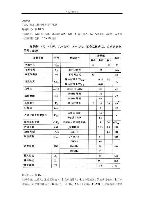
LM3915中文资料
为Байду номын сангаас子而狂热
LM3915
用途:发光二极管电平指示电路 封装形式:双 18-3 引脚功能:1.输出;2.地;3.电源 Vcc;4.地;5.信号输入;6,7.基准电压调整;9.条状 火点状现实选择;10~18.输出
封装形式:双 16 一 l。 引脚功能:1.输入;2.前置级输入;3.左声道输入;4.左声道输出;5.右声道输出;6.右声 道输入;7.立体声指示灯;8.地;9.开关门限;10.开关门限;11.19kHz 导频输出/声道
为电子而狂热
分离控制;12.解码输入;13.环路滤波;14.环叠备滤波;15.振荡器 Rc 网络;16.电源 V cc. 内部方框及典型应用电路:
同类直接代换型号:TcA4500A 电子狂客搜集整理于 2011-05-14
LM29150中文资料

-Leading Performance specifications ● Fixed Voltage and Adjustable VersionsAPPLICATIONS● Battery Powered Equipment● High-Efficiency " Green" Computer System ● Automotive Electronics● High-Efficiency Linear Power Supplies ● High-Efficiency Post-Regulator For Switching SupplyORDERING INFORMATIONPinoutLM29150: Three Therminal DevicesLM29151: Five Therminal Fixed Voltage Devices LM29152: Adjustable with ON/OFF controlLM29153: Adjustable with Flag * LM29151 - X.X (X.X = Output Voltage = 1.5V, 2.5V, 3.0V, 3.3V, 5.0V, 12V `DESCRIPTIONThe LM29150 are high current, high accuracy, low-dropout voltage regulators. Using process with a PNP pass element, these regulators feature 350mV (full load) dropout voltages and very low ground current.These devices also find applications in lower current, low dropout-critical systems, where their tiny dropout voltage and graound current values are important attributes.The LM29150 are fully protected against over current faults, reversed input polarity, reversed lead insertion, over temperature operation, and positive and negative transient voltage spikes. Five pin fixed voltage versions feature logic level ON/OFF control and an error flag which signals whenever the output falls out of regulation.On the LM29150 and LM29152, the ENABLE pin may be tied to Vin if it is not required for ON/OFF control.The LM29150 are available in 3- and 5- pinTO-220 and surface mount TO-263 packages.LM29150 - X.X LM29150RS - X.X LM29152/3LM29152RS/3RS - X.X LM29152/3DeviceLM29152R/3R LM29150R - X.X LM29151 - X.X LM29151RS - X.X LM29151R - X.X TO-263 5LMarkingLM29150 - X.X LM29151 - X.X TO-252 5LTO-263 5LTO-220 5LPin 1= Input, 2= Ground, 3= Output Package TO-220 3L TO-252 5L Pin 1= Flag, 2= Input, 3=Ground, 4=Output, 5= Adjust Pin 1= Enable, 2= Input, 3=Ground, 4=Output, 5= Adjust Pin 1= Enable, 2= Input, 3=Ground, 4=Output, 5= Flag TO-252 3L TO-263 3L TO-220 5L TO-263 3/5LTO-252 3/5LBlock Diagram and typical Application Circuit94[ Block Diagram ]* Feed Back network in fixed versions only **Adjustable version onlyVout=1.240V x [1+(R1/R2)]Figure2. Adjstable output voltageconfiguration. For best results, the totalseries resistance should be small enough to pass the minimum regulator load currentLMABSOULTE MAXIMUM RATINGSLead Temperature(Soldering, 5 Seconds)Storage Temperature Range Input Supply Voltage(Note 1)OPERATING RATINGSOperating Junction Temperature Maximum Operating Input VoltageELECTRICAL CHARACTERISTICS IOUT =100㎃, T A =25℃, unless otherwise specifiedAll measurements at Tj=25℃ unless otherwise noted. Bold Values are guaranteed across the operating temperature range.Adjustable versions are programmed to 5.0V-40℃ to + 125℃'26VCHARACTERISTICInternally Limit -20℃ to + 60℃'Internally LimitCHARACTERISTIC260℃-65℃ to + 150℃LM29150LM29152[ Note. ]1. Maximum positive supply voltage of 60V must be of limited duration (<100msec) and duty cycle(≤1%). The maximum continuous supply voltage is 26V2. Full load current(IFL ) is defined as 1.5A3. Dropout voltage is defined as the input-to-output differential when the output voltage drops to 99% of its nominal value with Vout to Vin4. Vin = Vout(nominal) +1V. For example, use Vin =4.3V for a 3.3V regulator or use 6V for a 5V regulator. Employ pulse-testing procedures to minimize temperature rise.5. Ground pin current is the regulator quiescent current. The total current drawn from the source is the sum of the load current plus the ground pin current.6. Output voltage temperature coefficient is defined as the worst case voltage change divided by the total temperature range.7. Thermal regulation is defined as the change in output voltage at a time T after a change in power dissipation is applied, excluding load or line regulation effects. Specifications are for a 200mA load pulse at Vin= 20V (a 4W pulse) for T= 10ms8. Vref ≤ Vout ≤ (Vin -1V), 2.3V ≤ Vin ≤ 26V, 10mA<IL IFL, TJ< TJ Max9. Comparator thresholds are expressed in terms of a voltage differential at the Adjust terminal below the nominal reference voltage measured at. 6V input. To express these thresholds in terms of output voltage change,multiply by the error amplifier gain = Vout/Vref = (R1 +R2)/R2. For example, at a programmed output voltage of 5V, the Error output is guaranteed to go low when the output drops by 95mV x 5V/ 1.240V - 384mV.Thresholds remain constant as a percent of Vout as Vout is varied, with the dropout warining occurring at typically 5% below nominal, 7.7% guaranteed.10. Ven ≤ 0.8V and Vin≤26V, Vout=011. When used in dual supply system where the regulator load is returned to a negative supply, the output Voltage must be diode clamped to ground.TYPICAL PERFORMANCE CHARACTERISTICSFigure 1. LM29150 Dropout Voltage vs,Output Current Figure 2. LM29150 Dropout Voltage vs,TemperatureFigure 3. LM29150- 5.0 DropoutCharacteristicsFigure 4. LM29150 Ground Current vs,Supply Voltage Figure 5. LM29150 Ground Current vs,TemperatureFigure 6. LM29150 Ground Current vs,TemperatureFigure 7. LM29150-3.3 Output Voltage vs.Temperature Figure 8. LM29150-3.3 Short CircuitCurrent vs. TemperatureFigure 9. LM29150 Ground Current vs.Input VoltageApplications InformationThe LM29150 are high performance low-dropout voltage regulators suitable for all moderate to high -current voltage regulator applications. Their 350mV dropout voltage at full load make them especially valuable in battery powered systems and as high efficiency noise filters in"post-regulator" applications. Unlike older NPN-pass transistor designs, dropout performance of the PNP output of these devices is limited merely by the low Vce saturation voltage.The LM29150 family of regulators is fully protected from damage due to fault conditions. Current Limiting is provided. This limiting is linear; output current under overload conditions is constant. Thermal shutdown disables the device when the die temperature exceeds the 125℃ maximum safe operating temperature. Transient protection allows device survival even when the input voltage spikes between -20V and +60V. When the input voltage exceeds about 35V to 40V. The over voltage sensor temporarily disables the regulator.Figure 3. Linear regulators require only two capacitorsfor operation.Thermal DesignLinear regulators are simple to use. The most complicated design parameters to consider are thermal characteristics. Thermal design requires the following application-specific parameters: *Maximum ambient temperature, T A*Output Current, I OUT*Output Voltage, V OUT*Input Voltage, V INFirst, we calculate the power dissipation of the regulator from these numbers and the device parameters from this datasheet.P D=I OUT(1.01V IN-V OUT)Where the ground current is approximated by 1% of I OUT. Then the heat sink thermalresistance is determined with this formula:Where TJ MAX≤ 125℃ and ΘCS is between 0 and 2℃/W.Capaitor RequirementsFor stability and minimum output noise,a capacitor on the regulator output is necessary. Thevalue of this capacitor is dependent upon the output current; lower currents allow smaller capcitors. LM29150 regulators are stable with the 10uF minimum capacitor values at full load. Where the regulator is powered from a source with a high AC impedance, a 0.1uF capacitor connected between input and GND is recommended. This capacitor should have good characteristics to above 250kHz.Minimum Load CurrentThe LM29150 regulators are specified between finite loads. If the output is too small, leakage currents is too small, leakage currents dominate and the output voltage rises. The 5mA minimum load current swamps any expected leakage current across the operating temperature range.Adjustable Regulator DesignFigure 4.Adjustable Regulator with ResistorsThe adjustable regulator versions, LM29152 and LM29153, allow programming the output voltage anywhere between 1.25V and the 26V maximum operating rating of the family.Two resistors are used. Resistors can be quite large, up to 1MΩ, because of the very high input impedance and low bias current of the sense comparator: The resistor values are calculated by:Where is VO the desired output voltage. Figure 4 shows component definition. Applications with widely varying load currents may scale the resistors to draw the minimum load current required for proper operation.Error FlagLM29151 and LM29153 versions feature and Error Flag, which looks at the output voltage and signals and error condition when this voltage and signals an error condition when this voltage drops 5% below its expected value. The error flag is an open-collector output that pulls low under fault conditions. It may sink 10mA. Low output voltage signifies a number of possible problems, including an over-current fault (the device is in current limit) and low input voltage.The flag output is inoperative during over temperature shutdwon conditions.Enable inputLM29151 and LM29152 versions feature and enable (EN) input that allows ON/OFF control of the device. Special design allows "zero" current drain when the device is disabled-only microamperes of leakage current flows. The EN input has TTL/CMOS compatible thresholds for simple interfacing with logic, or may be directly tied to ≤ 30V. Enabling the regulator requires approximately 20uA of current.VOUT=1.240V x [ 1+(R1/R2)]。
LM285-2.5中文资料

PACKAGING INFORMATIONOrderable Device Status(1)PackageType PackageDrawingPins PackageQtyEco Plan(2)Lead/Ball Finish MSL Peak Temp(3)LM285D-2-5ACTIVE SOIC D875Pb-Free(RoHS)CU NIPDAU Level-2-250C-1YEARLM285DR-2-5ACTIVE SOIC D82500Pb-Free(RoHS)CU NIPDAU Level-2-250C-1YEAR LM285LP-2-5ACTIVE TO-92LP31000None Call TI Level-NC-NC-NC LM285LPR-2-5ACTIVE TO-92LP32000None Call TI Level-NC-NC-NC LM385BD-2-5ACTIVE SOIC D875Pb-Free(RoHS)CU NIPDAU Level-2-250C-1YEARLM385BDR-2-5ACTIVE SOIC D82500Pb-Free(RoHS)CU NIPDAU Level-2-250C-1YEAR LM385BLP-2-5ACTIVE TO-92LP31000None Call TI Level-NC-NC-NC LM385BLPR-2-5ACTIVE TO-92LP32000None Call TI Level-NC-NC-NC LM385BPW-2-5ACTIVE TSSOP PW8150Pb-Free(RoHS)CU NIPDAU Level-1-250C-UNLIMLM385BPWR-2-5ACTIVE TSSOP PW82000Pb-Free(RoHS)CU NIPDAU Level-1-250C-UNLIMLM385D-2-5ACTIVE SOIC D875Pb-Free(RoHS)CU NIPDAU Level-2-250C-1YEARLM385DR-2-5ACTIVE SOIC D82500Pb-Free(RoHS)CU NIPDAU Level-2-250C-1YEAR LM385LP-2-5ACTIVE TO-92LP31000None Call TI Level-NC-NC-NC LM385LPR-2-5ACTIVE TO-92LP32000None Call TI Level-NC-NC-NC LM385PW-2-5ACTIVE TSSOP PW8150Pb-Free(RoHS)CU NIPDAU Level-1-250C-UNLIMLM385PWR-2-5ACTIVE TSSOP PW82000Pb-Free(RoHS)CU NIPDAU Level-1-250C-UNLIM(1)The marketing status values are defined as follows:ACTIVE:Product device recommended for new designs.LIFEBUY:TI has announced that the device will be discontinued,and a lifetime-buy period is in effect.NRND:Not recommended for new designs.Device is in production to support existing customers,but TI does not recommend using this part in a new design.PREVIEW:Device has been announced but is not in production.Samples may or may not be available.OBSOLETE:TI has discontinued the production of the device.(2)Eco Plan-May not be currently available-please check /productcontent for the latest availability information and additional product content details.None:Not yet available Lead(Pb-Free).Pb-Free(RoHS):TI's terms"Lead-Free"or"Pb-Free"mean semiconductor products that are compatible with the current RoHS requirements for all6substances,including the requirement that lead not exceed0.1%by weight in homogeneous materials.Where designed to be soldered at high temperatures,TI Pb-Free products are suitable for use in specified lead-free processes.Green(RoHS&no Sb/Br):TI defines"Green"to mean"Pb-Free"and in addition,uses package materials that do not contain halogens, including bromine(Br)or antimony(Sb)above0.1%of total product weight.(3)MSL,Peak Temp.--The Moisture Sensitivity Level rating according to the JEDECindustry standard classifications,and peak solder temperature.Important Information and Disclaimer:The information provided on this page represents TI's knowledge and belief as of the date that it is provided.TI bases its knowledge and belief on information provided by third parties,and makes no representation or warranty as to the accuracy of such information.Efforts are underway to better integrate information from third parties.TI has taken and continues to take reasonable steps to provide representative and accurate information but may not have conducted destructive testing or chemical analysis on incoming materials and chemicals.TI and TI suppliers consider certain information to be proprietary,and thus CAS numbers and other limitedinformation may not be available for release.In no event shall TI's liability arising out of such information exceed the total purchase price of the TI part(s)at issue in this document sold by TIto Customer on an annual basis.元器件交易网IMPORTANT NOTICETexas Instruments Incorporated and its subsidiaries (TI) reserve the right to make corrections, modifications,enhancements, improvements, and other changes to its products and services at any time and to discontinueany product or service without notice. Customers should obtain the latest relevant information before placingorders and should verify that such information is current and complete. All products are sold subject to TI’s termsand conditions of sale supplied at the time of order acknowledgment.TI warrants performance of its hardware products to the specifications applicable at the time of sale inaccordance with TI’s standard warranty. T esting and other quality control techniques are used to the extent TIdeems necessary to support this warranty. Except where mandated by government requirements, testing of allparameters of each product is not necessarily performed.TI assumes no liability for applications assistance or customer product design. Customers are responsible fortheir products and applications using TI components. T o minimize the risks associated with customer productsand applications, customers should provide adequate design and operating safeguards.TI does not warrant or represent that any license, either express or implied, is granted under any TI patent right,copyright, mask work right, or other TI intellectual property right relating to any combination, machine, or processin which TI products or services are used. Information published by TI regarding third-party products or servicesdoes not constitute a license from TI to use such products or services or a warranty or endorsement thereof.Use of such information may require a license from a third party under the patents or other intellectual propertyof the third party, or a license from TI under the patents or other intellectual property of TI.Reproduction of information in TI data books or data sheets is permissible only if reproduction is withoutalteration and is accompanied by all associated warranties, conditions, limitations, and notices. Reproductionof this information with alteration is an unfair and deceptive business practice. TI is not responsible or liable forsuch altered documentation.Resale of TI products or services with statements different from or beyond the parameters stated by TI for thatproduct or service voids all express and any implied warranties for the associated TI product or service andis an unfair and deceptive business practice. TI is not responsible or liable for any such statements.Following are URLs where you can obtain information on other Texas Instruments products and applicationsolutions:Products ApplicationsAmplifiers Audio /audioData Converters Automotive /automotiveDSP Broadband /broadbandInterface Digital Control /digitalcontrolLogic Military /militaryPower Mgmt Optical Networking /opticalnetworkMicrocontrollers Security /securityTelephony /telephonyVideo & Imaging /videoWireless /wirelessMailing Address:Texas InstrumentsPost Office Box 655303 Dallas, Texas 75265Copyright 2005, Texas Instruments Incorporated。
LM285Z-2.5中文资料(简)

封装信息
� � Z PACKAGE/3-LEAD T0-92 PLASTIC(三脚 T0-92 塑料封装) S8 PACKAGE /8-LEAD PLASTIC S0(八脚贴片封装)
电气特性及封装尺寸
均参考英文版资料
LM185/285/285
特性
� � � � 20uA 至 20mA 工作范围 保证 1%初始电压容差 保证 1 便携式仪表(电表)参考 便携式测试仪器 电池供电系统 数显电测量仪表 电流回路仪器仪表
描述
LM285-2.5 是一个被设计用于需要那些精确性能和微操作应用的双端带隙参考二极管。 该器 件可在低至 20uA 的电流下保证操作的规范。在 1%至 2%的允许公差下,标称电压为 2.5V。 还有一些别的特性,包括:在时间的推移和温度的变化下,拥有 1 欧姆的最大动态阻抗, 低 噪声和出色的稳定性。先进的设计,加工和测试技术使得线性 LM185-2.5 成为过去设计中 的上乘选择。热电偶冷端补偿电路如下图所示。 为了满足保证温度漂移的应用,可参考 LT1034 的数据表。
典型应用
绝对最大额定值
反向击穿电流。 。 。 。 。 。 。 。 。 。 。 。 。 。30mA 正向电流。 。 。 。 。 。 。 。 。 。 。 。 。 。 。 。 。 。10mA 操作温度范围(单位:摄氏度) LM185-2.5(过时) 。 。 。 。 。 。-55~125 LM285-2.5。 。 。 。 。 。 。 。 。 。 。 。 。-40~85 LM385-2.5。 。 。 。 。 。 。 。 。 。 。 。 。0~70 存储温度范围(单位:摄氏度) LM185-2.5(过时) 。 。 。 。 。 。-65~150 LM285-2.5。 。 。 。 。 。 。 。 。 。 。 。 。-65~150 LM385-2.5。 。 。 。 。 。 。 。 。 。 。 。 。-65~150 导线温度(焊接,10 秒) 。 。 。 。 。 。 。 。.300
LM4050AEM3-2.5中文资料
LM4050Precision Micropower Shunt Voltage ReferenceGeneral DescriptionIdeal for space critical applications,the LM4050precision voltage reference is available in the sub-miniature (3mm x 1.3mm)SOT-23surface-mount package.The LM4050’s de-sign eliminates the need for an external stabilizing capacitor while ensuring stability with any capacitive load,thus making the LM4050easy to use.Further reducing design effort is the availability of several fixed reverse breakdown voltages:2.048V,2.500V,4.096V,5.000V,8.192V,and 10.000V.The minimum operating current increases from 60µA for the LM4050-2.0to 100µA for the LM4050-10.0.All versions have a maximum operating current of 15mA.The LM4050utilizes fuse and zener-zap reverse breakdown voltage trim during wafer sort to ensure that the prime parts have an accuracy of better than ±0.1%(A grade)at 25˚C.Bandgap reference temperature drift curvature correction and low dynamic impedance ensure stable reverse break-down voltage accuracy over a wide range of operating tem-peratures and currents.All grades and voltage options of the LM4050are available in both an industrial temperature range (−40˚C and +85˚C)and an extended temperature range (−40˚C and +125˚C).Featuresn Small packages:SOT-23n No output capacitor requiredn Tolerates capacitive loadsn Fixed reverse breakdown voltages of 2.048V,2.500V,4.096V,5.000V,8.192V,and 10.000VKey Specifications (LM4050-2.5)j Output voltage tolerance(A grade,25˚C)±0.1%(max)j Low output noise(10Hz to 10kHz)41µV rms (typ)j Wide operating current range 60µA to 15mA j Industrial temperature range −40˚C to +85˚C j Extended temperature range −40˚C to +125˚C j Low temperature coefficient50ppm/˚C (max)Applicationsn Portable,Battery-Powered Equipment n Data Acquisition Systems n Instrumentation n Process Controln Energy Management n Product Testing n AutomotivenPrecision Audio ComponentsConnection DiagramSOT-2310104501*This pin must be left floating or connected to pin 2.Top ViewSee NS Package Number MF03AJuly 2004LM4050Precision Micropower Shunt Voltage Reference©2004National Semiconductor Corporation Ordering InformationIndustrial Temperature Range (−40˚C to +85˚C)Reverse BreakdownVoltage Tolerance at 25˚C and AverageReverse BreakdownVoltage Temperature CoefficientLM4050Supplied as 1000Units,Tape and ReelLM4050Supplied as 3000Units,Tape and ReelLM4050AIM3-2.0LM4050AIM3X-2.0±0.1%,50ppm/˚C max (A grade)LM4050AIM3-2.5LM4050AIM3X-2.5LM4050AIM3-4.1LM4050AIM3X-4.1LM4050AIM3-5.0LM4050AIM3X-5.0LM4050AIM3-8.2LM4050AIM3X-8.2LM4050AIM3-10LM4050AIM3X-10LM4050BIM3-2.0LM4050BIM3X-2.0±0.2%,50ppm/˚C max (B grade)LM4050BIM3-2.5LM4050BIM3X-2.5LM4050BIM3-4.1LM4050BIM3X-4.1LM4050BIM3-5.0LM4050BIM3X-5.0LM4050BIM3-8.2LM4050BIM3X-8.2LM4050BIM3-10LM4050BIM3X-10LM4050CIM3-2.0LM4050CIM3X-2.0±0.5%,50ppm/˚C max (C grade)LM4050CIM3-2.5LM4050CIM3X-2.5LM4050CIM3-4.1LM4050CIM3X-4.1LM4050CIM3-5.0LM4050CIM3X-5.0LM4050CIM3-8.2LM4050CIM3X-8.2LM4050CIM3-10LM4050CIM3X-10Extended Temperature Range (−40˚C to +125˚C)Reverse BreakdownVoltage Tolerance at 25˚C and AverageReverse BreakdownVoltage Temperature CoefficientLM4050Supplied as 1000Units,Tape and ReelLM4050Supplied as 3000Units,Tape and ReelLM4050AEM3-2.0LM4050AEM3X-2.0±0.1%,50ppm/˚C max (A grade)LM4050AEM3-2.5LM4050AEM3X-2.5LM4050AEM3-4.1LM4050AEM3X-4.1LM4050AEM3-5.0LM4050AEM3X-5.0LM4050AEM3-8.2LM4050AEM3X-8.2LM4050AEM3-10LM4050AEM3X-10LM4050BEM3-2.0LM4050BEM3X-2.0±0.2%,50ppm/˚C max (B grade)LM4050BEM3-2.5LM4050BEM3X-2.5LM4050BEM3-4.1LM4050BEM3X-4.1LM4050BEM3-5.0LM4050BEM3X-5.0LM4050BEM3-8.2LM4050BEM3X-8.2LM4050BEM3-10LM4050BEM3X-10LM4050CEM3-2.0LM4050CEM3X-2.0±0.5%,50ppm/˚C max (C grade)LM4050CEM3-2.5LM4050CEM3X-2.5LM4050CEM3-4.1LM4050CEM3X-4.1LM4050CEM3-5.0LM4050CEM3X-5.0LM4050CEM3-8.2LM4050CEM3X-8.2LM4050CEM3-10LM4050CEM3X-10L M 4050 2LM4050 SOT-23Package Marking InformationOnly three fields of marking are possible on the SOT-23’s small surface.This table gives the meaning of the three fields.Part Marking Field DefinitionRCA First Field:RDA R=ReferenceREA Second Field:RFA N=2.048V Voltage OptionRGA C=2.500V Voltage OptionRNA D=4.096V Voltage OptionRCB E=5.000V Voltage OptionRDB F=8.192V Voltage OptionREB G=10.000V Voltage OptionRFBRGB Third Field:RNBRCC A–C=Initial Reverse Breakdown Voltage or Reference Voltage ToleranceRDC A=±0.1%,B=±0.2%,C=+0.5%,RECRFCRGCRNC3Absolute Maximum Ratings (Note 1)If Military/Aerospace specified devices are required,please contact the National Semiconductor Sales Office/Distributors for availability and specifications.Reverse Current 20mA Forward Current10mAPower Dissipation (T A =25˚C)(Note 2)M3Package 280mWStorage Temperature −65˚C to +150˚CLead Temperature M3PackageVapor phase (60seconds)+215˚C Infrared (15seconds)+220˚C ESD SusceptibilityHuman Body Model (Note 3)2kV Machine Model (Note 3)200V See AN-450“Surface Mounting Methods and Their Effect on Product Reliability”for other methods of soldering surface mount devices.Operating Ratings (Note 2)Temperature Range (T min ≤T A ≤T max )Industrial Temperature Range−40˚C ≤T A ≤+85˚C Extended temperature Range−40˚C ≤T A ≤+125˚CReverse Current LM4050-2.060µA to 15mA LM4050-2.560µA to 15mA LM4050-4.168µA to 15mA LM4050-5.074µA to 15mA LM4050-8.291µA to 15mA LM4050-10.0100µA to 15mA LM4050-2.0Electrical CharacteristicsBoldface limits apply for T A =T J =T MIN to T MAX ;all other limits T A =T J =25˚C.The grades A,B and C designate initial Reverse Breakdown Voltage tolerances of ±0.1%,±0.2%,and 0.5%respectively.Symbol ParameterConditionsTypical (Note 4)LM4050AIM3LM4050AEM3Limits (Note 5)LM4050BIM3LM4050BEM3Limits (Note 5)LM4050CIM3LM4050CEM3Limits (Note 5)Units (Limit)V RReverse Breakdown Voltage I R =100µA 2.048VReverse Breakdown Voltage Tolerance (Note 6)I R =100µA±2.048±4.096±10.24mV (max)Industrial Temp.Range ±9.0112±11.4688±14.7456mV (max)Extended Temp.Range±12.288±14.7456±17.2032mV (max)I RMINMinimum Operating Current41µA 606060µA (max)656565µA (max)∆V R /∆TAverage Reverse Breakdown Voltage Temperature Coefficient (Note 6)I R =10mA ±20ppm/˚C I R =1mA ±15ppm/˚CI R =100µA±15±50±50±50ppm/˚C (max)∆V R /∆I RReverse Breakdown Voltage Change with Operating Current Change (Note 7)I RMIN ≤I R ≤1mA0.3mV 0.80.80.8mV (max)1.21.2 1.2mV (max)1mA ≤I R ≤15mA2.3mV 6.0 6.0 6.0mV (max)8.08.08.0mV (max)Z R Reverse Dynamic Impedance I R =1mA,f =120Hz,I AC =0.1I R 0.3Ωe N Wideband NoiseI R =100µA 34µV rms10Hz ≤f ≤10kHz ∆V R Reverse Breakdown Voltage Long Term Stability t =1000hrsT =25˚C ±0.1˚C I R =100µA120ppm V HYSTThermal Hysteresis (Note 8)∆T =−40˚C to 125˚C0.7mVL M 4050 4LM4050-2.5Electrical CharacteristicsBoldface limits apply for T A=T J=T MIN to T MAX;all other limits T A=T J=25˚C.The grades A,B and C designate initial Reverse Breakdown Voltage tolerances of±0.1%,±0.2%,and0.5%respectively.Symbol Parameter Conditions Typical(Note4)LM4050AIM3LM4050AEM3Limits(Note5)LM4050BIM3LM4050BEM3Limits(Note5)LM4050CIM3LM4050CEM3Limits(Note5)Units(Limit)V R Reverse Breakdown Voltage I R=100µA 2.500VReverse Breakdown Voltage Tolerance(Note6)I R=100µA±2.5±5.0±13mV(max) Industrial Temp.Range±11±14±21mV(max) Extended Temp.Range±15±18±25mV(max)I RMIN Minimum Operating Current41µA606060µA(max)656565µA(max)∆V R/∆T Average Reverse BreakdownVoltage Temperature Coefficient(Note6)I R=10mA±20ppm/˚CI R=1mA±15ppm/˚CI R=100µA±15±50±50±50ppm/˚C(max)∆V R/∆I R Reverse Breakdown VoltageChange with Operating CurrentChange(Note7)I RMIN≤I R≤1mA0.3mV0.80.80.8mV(max)1.2 1.2 1.2mV(max) 1mA≤I R≤15mA2.3mV6.0 6.0 6.0mV(max)8.08.08.0mV(max)Z R Reverse Dynamic Impedance I R=1mA,f=120Hz,I AC=0.1I R0.3Ωe N Wideband Noise I R=100µA41µV rms10Hz≤f≤10kHz∆V R Reverse Breakdown VoltageLong Term Stability t=1000hrsT=25˚C±0.1˚CI R=100µA120ppmV HYST Thermal Hysteresis(Note8)∆T=−40˚C to125˚C0.7mVLM4050-4.1Electrical CharacteristicsBoldface limits apply for T A=T J=T MIN to T MAX;all other limits T A=T J=25˚C.The grades A,B and C designate initial Reverse Breakdown Voltage tolerances of±0.1%,±0.2%,and0.5%respectively.Symbol Parameter Conditions Typical(Note4)LM4050AIM3LM4050AEM3Limits(Note5)LM4050BIM3LM4050BEM3Limits(Note5)LM4050CIM3LM4050CEM3Limits(Note5)Units(Limit)V R Reverse Breakdown Voltage I R=100µA 4.096VReverse Breakdown Voltage Tolerance(Note6)I R=100µA±4.1±8.2±21mV(max) Industrial Temp.Range±18±22±34mV(max) Extended Temp.Range±25±29±41mV(max)I RMIN Minimum Operating Current52µA686868µA(max)Industrial Temp.Range737373µA(max)Extended Temp.Range787878µA(max)∆V R/∆T Average Reverse BreakdownVoltage Temperature Coefficient(Note6)I R=10mA±30ppm/˚CI R=1mA±20ppm/˚CI R=100µA±20±50±50±50ppm/˚C(max)∆V R/∆I R Reverse Breakdown VoltageChange with Operating CurrentChange(Note7)I RMIN≤I R≤1mA0.2mV0.90.90.9mV(max)1.2 1.2 1.2mV(max)1mA≤I R≤15mA 2.0mV7.07.07.0mV(max)10.010.010.0mV(max)LM40505LM4050-4.1Electrical Characteristics(Continued)Boldface limits apply for T A =T J =T MIN to T MAX ;all other limits T A =T J =25˚C.The grades A,B and C designate initial Reverse Breakdown Voltage tolerances of ±0.1%,±0.2%,and 0.5%respectively.Symbol ParameterConditionsTypical (Note 4)LM4050AIM3LM4050AEM3Limits (Note 5)LM4050BIM3LM4050BEM3Limits (Note 5)LM4050CIM3LM4050CEM3Limits (Note 5)Units(Limit)Z R Reverse Dynamic Impedance I R =1mA,f =120Hz,0.5ΩI AC =0.1I R e N Wideband NoiseI R =100µA 93µV rms10Hz ≤f ≤10kHz ∆V R Reverse Breakdown Voltage Long Term Stability t =1000hrsT =25˚C ±0.1˚C I R =100µA120ppm V HYSTThermal Hysteresis (Note 8)∆T =−40˚C to 125˚C1.148mVLM4050-5.0Electrical CharacteristicsBoldface limits apply for T A =T J =T MIN to T MAX ;all other limits T A =T J =25˚C.The grades A,B and C designate initial Reverse Breakdown Voltage tolerances of ±0.1%,±0.2%and 0.5%respectively.Symbol ParameterConditionsTypical (Note 4)LM4050AIM3LM4050AEM3Limits (Note 5)LM4050BIM3LM4050BEM3Limits (Note 5)LM4050CIM3LM4050CEM3Limits (Note 5)Units(Limit)V RReverse Breakdown Voltage I R =100µA 5.000VReverse Breakdown Voltage Tolerance (Note 6)I R =100µA±5.0±10±25mV (max)Industrial Temp.Range ±22±27±42mV (max)Extended Temp.Range±30±35±50mV (max)I RMINMinimum Operating Current56µA 747474µA (max)Industrial Temp.Range 808080µA (max)Extended Temp.Range909090µA (max)∆V R /∆TAverage Reverse Breakdown Voltage Temperature Coefficient (Note 6)I R =10mA ±30ppm/˚C I R =1mA ±20ppm/˚CI R =100µA±20±50±50±50ppm/˚C (max)∆V R /∆I RReverse Breakdown Voltage Change with Operating Current Change (Note 7)I RMIN ≤I R ≤1mA0.2mV 1.0 1.0 1.0mV (max)1.41.4 1.4mV (max)1mA ≤I R ≤15mA2.0mV 8.08.08.0mV (max)12.012.012.0mV (max)Z R Reverse Dynamic Impedance I R =1mA,f =120Hz,0.5ΩI AC =0.1I R Ω(max)e N Wideband NoiseI R =100µA 93µV rms10Hz ≤f ≤10kHz ∆V RReverse Breakdown Voltage Long Term Stabilityt =1000hrs T =25˚C ±0.1˚C 120ppmI R =100µAV HYSTThermal Hysteresis (Note 8)∆T =−40˚C to 125˚C1.4mVL M 4050 6LM4050-8.2Electrical CharacteristicsBoldface limits apply for T A=T J=T MIN to T MAX;all other limits T A=T J=25˚C.The grades A,B and C designate initial Reverse Breakdown Voltage tolerances of±0.1%and±0.2%and0.5%respectively.Symbol Parameter Conditions Typical(Note4)LM4050AIM3LM4050AEM3Limits(Note5)LM4050BIM3LM4050BEM3Limits(Note5)LM4050CIM3LM4050CEM3Limits(Note5)Units(Limit)V R Reverse Breakdown Voltage I R=150µA8.192VReverse Breakdown Voltage Tolerance(Note6)I R=150µA±8.2±16±41mV(max) Industrial Temp.Range±35±43±68mV(max) Extended Temp.Range±49±57±82mV(max)I RMIN Minimum Operating Current74µA919191µA(max)Industrial Temp.Range959595µA(max)Extended Temp.Range100100100µA(max)∆V R/∆T Average Reverse BreakdownVoltage Temperature Coefficient(Note6)I R=10mA±40ppm/˚CI R=1mA±20ppm/˚CI R=150µA±20±50±50±50ppm/˚C(max)∆V R/∆I R Reverse Breakdown VoltageChange with Operating CurrentChange(Note7)I RMIN≤I R≤1mA0.6mV1.3 1.3 1.3mV(max)2.5 2.5 2.5mV(max) 1mA≤I R≤15mA7.0mV10.010.010.0mV(max)18.018.018.0mV(max)Z R Reverse Dynamic Impedance I R=1mA,f=120Hz,0.6ΩI AC=0.1I Re N Wideband Noise I R=150µA150µV rms10Hz≤f≤10kHz∆V R Reverse Breakdown VoltageLong Term Stability t=1000hrsT=25˚C±0.1˚C120ppm I R=150µAV HYST Thermal Hysteresis(Note8)∆T=−40˚C to125˚C 2.3mVLM40507LM4050-10.0Electrical CharacteristicsBoldface limits apply for T A =T J =T MIN to T MAX ;all other limits T A =T J =25˚C.The grades A,B and C designate initial Reverse Breakdown Voltage tolerances of ±0.1%and ±0.2%and 0.5%respectively.Symbol ParameterConditionsTypical (Note 4)LM4050AIM3LM4050AEM3Limits (Note 5)LM4050BIM3LM4050BEM3Limits (Note 5)LM4050CIM3LM4050CEM3Limits (Note 5)Units(Limit)V RReverse Breakdown Voltage I R =150µA 10.00VReverse Breakdown Voltage Tolerance (Note 6)I R =150µA±10±20±50mV (max)Industrial Temp.Range ±43±53±83mV (max)Extended Temp.Range±60±70±100mV (max)I RMINMinimum Operating Current80µA 100100100µA (max)Industrial Temp.Range 103103103µA (max)Extended Temp.Range110110110µA (max)∆V R /∆TAverage Reverse Breakdown Voltage Temperature Coefficient (Note 6)I R =10mA ±40ppm/˚C I R =1mA ±20ppm/˚CI R =150µA±20±50±50±50ppm/˚C (max)∆V R /∆I RReverse Breakdown Voltage Change with Operating Current Change (Note 7)I RMIN ≤I R ≤1mA0.8mV 1.5 1.5 1.5mV (max)3.53.5 3.5mV (max)1mA ≤I R ≤15mA 8.0mV 12.012.012.0mV (max)23.023.023.0mV (max)Z R Reverse Dynamic Impedance I R =1mA,f =120Hz,0.7ΩI AC =0.1I R e N Wideband NoiseI R =150µA 150µV rms10Hz ≤f ≤10kHz ∆V RReverse Breakdown Voltage Long Term Stabilityt =1000hrs T =25˚C ±0.1˚C 120ppmI R =150µAV HYSTThermal Hysteresis (Note 8)∆T =−40˚C to 125˚C2.8mVNote 1:Absolute Maximum Ratings indicate limits beyond which damage to the device may occur.Operating Ratings indicate conditions for which the device is functional,but do not guarantee specific performance limits.For guaranteed specifications and test conditions,see the Electrical Characteristics.The guaranteed specifications apply only for the test conditions listed.Some performance characteristics may degrade when the device is not operated under the listed test conditions.Note 2:The maximum power dissipation must be derated at elevated temperatures and is dictated by T Jmax (maximum junction temperature),θJA (junction to ambient thermal resistance),and T A (ambient temperature).The maximum allowable power dissipation at any temperature is PD max =(T Jmax −T A )/θJA or the number given in the Absolute Maximum Ratings,whichever is lower.For the LM4050,T Jmax =125˚C,and the typical thermal resistance (θJA ),when board mounted,is 326˚C/W for the SOT-23package.Note 3:The human body model is a 100pF capacitor discharged through a 1.5k Ωresistor into each pin.The machine model is a 200pF capacitor discharged directly into each pin.Note 4:Typicals are at T J =25˚C and represent most likely parametric norm.Note 5:Limits are 100%production tested at 25˚C.Limits over temperature are guaranteed through correlation using Statistical Quality Control (SQC)methods.The limits are used to calculate National’s AOQL.Note 6:The boldface (over-temperature)limit for Reverse Breakdown Voltage Tolerance is defined as the room temperature Reverse Breakdown Voltage Tolerance ±[(∆V R /∆T)(max ∆T)(V R )].Where,∆V R /∆T is the V R temperature coefficient,max ∆T is the maximum difference in temperature from the reference point of 25˚C to T MIN or T MAX ,and V R is the reverse breakdown voltage.The total over-temperature tolerance for the different grades in the industrial temperature range where max ∆T =65˚C is shown below:A-grade:±0.425%=±0.1%±50ppm/˚C x 65˚C B-grade:±0.525%=±0.2%±50ppm/˚C x 65˚C C-grade:±0.825%=±0.5%±50ppm/˚C x 65˚CTherefore,as an example,the A-grade LM4050-2.5has an over-temperature Reverse Breakdown Voltage tolerance of ±2.5V x 0.425%=±11mV.Note 7:Load regulation is measured on pulse basis from no load to the specified load current.Output changes due to die temperature change must be taken into account separately.Note 8:Thermal hysteresis is defined as the difference in voltage measured at +25˚C after cycling to temperature -40˚C and the 25˚C measurement after cycling to temperature +125˚C.L M 4050 8Typical Performance CharacteristicsOutput Impedance vs FrequencyOutput Impedance vs Frequency1010451010104511Reverse Characteristics and Minimum Operating CurrentNoise Voltage vs Frequency1010451210104513Thermal Hysteresis10104529LM40509Start-Up Characteristics10104505LM4050-2.5R S=30k10104507LM4050-5.0R S=30k10104508LM4050-10.0R S=30k10104509 LM4510Functional Block Diagram10104514Applications InformationThe LM4050is a precision micro-power curvature-corrected bandgap shunt voltage reference.For space critical applica-tions,the LM4050is available in the sub-miniature SOT-23surface-mount package.The LM4050has been designed for stable operation without the need of an external capacitor connected between the “+”pin and the “−”pin.If,however,a bypass capacitor is used,the LM4050remains stable.Re-ducing design effort is the availability of several fixed reverse breakdown voltages: 2.048V, 2.500V, 4.096V, 5.000V,8.192V,and 10.000V.The minimum operating current in-creases from 60µA for the LM4050-2.0to 100µA for the LM4050-10.0.All versions have a maximum operating cur-rent of 15mA.LM4050s in the SOT-23packages have a parasitic Schottky diode between pin 2(−)and pin 3(Die attach interface contact).Therefore,pin 3of the SOT-23package must be left floating or connected to pin 2.The 4.096V version allows single +5V 12-bit ADCs or DACs to operate with an LSB equal to 1mV.For 12-bit ADCs or DACs that operate on supplies of 10V or greater,the 8.192V version gives 2mV per LSB.The typical thermal hysteresis specification is defined as the change in +25˚C voltage measured after thermal cycling.The device is thermal cycled to temperature -40˚C and then measured at 25˚C.Next the device is thermal cycled totemperature +125˚C and again measured at 25˚C.The re-sulting V OUT delta shift between the 25˚C measurements is thermal hysteresis.Thermal hysteresis is common in preci-sion references and is induced by thermal-mechanical pack-age stress.Changes in environmental storage temperature,operating temperature and board mounting temperature are all factors that can contribute to thermal hysteresis.In a conventional shunt regulator application (Figure 1),an external series resistor (R S )is connected between the sup-ply voltage and the LM4050.R S determines the current that flows through the load (I L )and the LM4050(I Q ).Since load current and supply voltage may vary,R S should be small enough to supply at least the maximum guaranteed I RMIN (spec.table)to the LM4050even when the supply voltage is at its minimum and the load current is at its maximum value.When the supply voltage is at its maximum and I L is at its minimum,R S should be large enough so that the current flowing through the LM4050is less than 15mA.R S is determined by the supply voltage,(V S ),the load and operating current,(I L and I Q ),and the LM4050’s reverse breakdown voltage,V R .Typical Applications10104515FIGURE 1.Shunt RegulatorLM405011Typical Applications(Continued)10104516**Ceramic monolithic *TantalumFIGURE 2.LM4050-4.1’s Nominal 4.096breakdown voltage gives ADC124511mV/LSBL M 4050 12Typical Applications(Continued)10104517FIGURE 3.Bounded amplifier reduces saturation-induced delays and can prevent succeeding stage damage.Nominal clamping voltage is ±11.5V (LM4050’s reverse breakdown voltage +2diode V F ).10104518FIGURE 4.Protecting Op Amp input.The bounding voltage is ±4V with the LM4050-2.5(LM4050’s reverse breakdown voltage +3diode V F ).LM405013Typical Applications(Continued)10104519FIGURE 5.Precision ±4.096V Reference1010452110104522FIGURE 6.Precision 1µA to 1mA Current SourcesL M 4050 14Physical Dimensionsinches (millimeters)unless otherwise notedPlastic Surface Mount Package (M3)NS Package Number MF03A (JEDEC Registration TO-236AB)LIFE SUPPORT POLICYNATIONAL’S PRODUCTS ARE NOT AUTHORIZED FOR USE AS CRITICAL COMPONENTS IN LIFE SUPPORT DEVICES OR SYSTEMS WITHOUT THE EXPRESS WRITTEN APPROVAL OF THE PRESIDENT AND GENERAL COUNSEL OF NATIONAL SEMICONDUCTOR CORPORATION.As used herein:1.Life support devices or systems are devices or systems which,(a)are intended for surgical implant into the body,or (b)support or sustain life,and whose failure to perform when properly used in accordance with instructions for use provided in the labeling,can be reasonably expected to result in a significant injury to the user. 2.A critical component is any component of a life support device or system whose failure to perform can be reasonably expected to cause the failure of the life support device or system,or to affect its safety or effectiveness.BANNED SUBSTANCE COMPLIANCENational Semiconductor certifies that the products and packing materials meet the provisions of the Customer Products Stewardship Specification (CSP-9-111C2)and the Banned Substances and Materials of Interest Specification (CSP-9-111S2)and contain no ‘‘Banned Substances’’as defined in CSP-9-111S2.National Semiconductor Americas Customer Support CenterEmail:new.feedback@ Tel:1-800-272-9959National SemiconductorEurope Customer Support CenterFax:+49(0)180-5308586Email:europe.support@Deutsch Tel:+49(0)6995086208English Tel:+44(0)8702402171Français Tel:+33(0)141918790National Semiconductor Asia Pacific Customer Support CenterEmail:ap.support@National SemiconductorJapan Customer Support Center Fax:81-3-5639-7507Email:jpn.feedback@ Tel:81-3-5639-7560LM4050Precision Micropower Shunt Voltage ReferenceNational does not assume any responsibility for use of any circuitry described,no circuit patent licenses are implied and National reserves the right at any time without notice to change said circuitry and specifications.。
LM29152RS-2.5资料
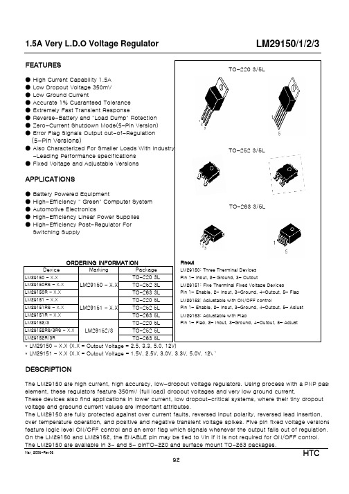
-Leading Performance specifications ● Fixed Voltage and Adjustable VersionsAPPLICATIONS● Battery Powered Equipment● High-Efficiency " Green" Computer System ● Automotive Electronics● High-Efficiency Linear Power Supplies ● High-Efficiency Post-Regulator For Switching SupplyORDERING INFORMATIONPinoutLM29150: Three Therminal DevicesLM29151: Five Therminal Fixed Voltage Devices LM29152: Adjustable with ON/OFF controlLM29153: Adjustable with Flag * LM29151 - X.X (X.X = Output Voltage = 1.5V, 2.5V, 3.0V, 3.3V, 5.0V, 12V `DESCRIPTIONThe LM29150 are high current, high accuracy, low-dropout voltage regulators. Using process with a PNP pass element, these regulators feature 350mV (full load) dropout voltages and very low ground current.These devices also find applications in lower current, low dropout-critical systems, where their tiny dropout voltage and graound current values are important attributes.The LM29150 are fully protected against over current faults, reversed input polarity, reversed lead insertion, over temperature operation, and positive and negative transient voltage spikes. Five pin fixed voltage versions feature logic level ON/OFF control and an error flag which signals whenever the output falls out of regulation.On the LM29150 and LM29152, the ENABLE pin may be tied to Vin if it is not required for ON/OFF control.The LM29150 are available in 3- and 5- pinTO-220 and surface mount TO-263 packages.LM29150 - X.X LM29150RS - X.X LM29152/3LM29152RS/3RS - X.X LM29152/3DeviceLM29152R/3R LM29150R - X.X LM29151 - X.X LM29151RS - X.X LM29151R - X.X TO-263 5LMarkingLM29150 - X.X LM29151 - X.X TO-252 5LTO-263 5LTO-220 5LPin 1= Input, 2= Ground, 3= Output Package TO-220 3L TO-252 5L Pin 1= Flag, 2= Input, 3=Ground, 4=Output, 5= Adjust Pin 1= Enable, 2= Input, 3=Ground, 4=Output, 5= Adjust Pin 1= Enable, 2= Input, 3=Ground, 4=Output, 5= Flag TO-252 3L TO-263 3L TO-220 5L TO-263 3/5LTO-252 3/5LBlock Diagram and typical Application Circuit94[ Block Diagram ]* Feed Back network in fixed versions only **Adjustable version onlyVout=1.240V x [1+(R1/R2)]Figure2. Adjstable output voltageconfiguration. For best results, the totalseries resistance should be small enough to pass the minimum regulator load currentLMABSOULTE MAXIMUM RATINGSLead Temperature(Soldering, 5 Seconds)Storage Temperature Range Input Supply Voltage(Note 1)OPERATING RATINGSOperating Junction Temperature Maximum Operating Input VoltageELECTRICAL CHARACTERISTICS IOUT =100㎃, T A =25℃, unless otherwise specifiedAll measurements at Tj=25℃ unless otherwise noted. Bold Values are guaranteed across the operating temperature range.Adjustable versions are programmed to 5.0V-40℃ to + 125℃'26VCHARACTERISTICInternally Limit -20℃ to + 60℃'Internally LimitCHARACTERISTIC260℃-65℃ to + 150℃LM29150LM29152[ Note. ]1. Maximum positive supply voltage of 60V must be of limited duration (<100msec) and duty cycle(≤1%). The maximum continuous supply voltage is 26V2. Full load current(IFL ) is defined as 1.5A3. Dropout voltage is defined as the input-to-output differential when the output voltage drops to 99% of its nominal value with Vout to Vin4. Vin = Vout(nominal) +1V. For example, use Vin =4.3V for a 3.3V regulator or use 6V for a 5V regulator. Employ pulse-testing procedures to minimize temperature rise.5. Ground pin current is the regulator quiescent current. The total current drawn from the source is the sum of the load current plus the ground pin current.6. Output voltage temperature coefficient is defined as the worst case voltage change divided by the total temperature range.7. Thermal regulation is defined as the change in output voltage at a time T after a change in power dissipation is applied, excluding load or line regulation effects. Specifications are for a 200mA load pulse at Vin= 20V (a 4W pulse) for T= 10ms8. Vref ≤ Vout ≤ (Vin -1V), 2.3V ≤ Vin ≤ 26V, 10mA<IL IFL, TJ< TJ Max9. Comparator thresholds are expressed in terms of a voltage differential at the Adjust terminal below the nominal reference voltage measured at. 6V input. To express these thresholds in terms of output voltage change,multiply by the error amplifier gain = Vout/Vref = (R1 +R2)/R2. For example, at a programmed output voltage of 5V, the Error output is guaranteed to go low when the output drops by 95mV x 5V/ 1.240V - 384mV.Thresholds remain constant as a percent of Vout as Vout is varied, with the dropout warining occurring at typically 5% below nominal, 7.7% guaranteed.10. Ven ≤ 0.8V and Vin≤26V, Vout=011. When used in dual supply system where the regulator load is returned to a negative supply, the output Voltage must be diode clamped to ground.TYPICAL PERFORMANCE CHARACTERISTICSFigure 1. LM29150 Dropout Voltage vs,Output Current Figure 2. LM29150 Dropout Voltage vs,TemperatureFigure 3. LM29150- 5.0 DropoutCharacteristicsFigure 4. LM29150 Ground Current vs,Supply Voltage Figure 5. LM29150 Ground Current vs,TemperatureFigure 6. LM29150 Ground Current vs,TemperatureFigure 7. LM29150-3.3 Output Voltage vs.Temperature Figure 8. LM29150-3.3 Short CircuitCurrent vs. TemperatureFigure 9. LM29150 Ground Current vs.Input VoltageApplications InformationThe LM29150 are high performance low-dropout voltage regulators suitable for all moderate to high -current voltage regulator applications. Their 350mV dropout voltage at full load make them especially valuable in battery powered systems and as high efficiency noise filters in"post-regulator" applications. Unlike older NPN-pass transistor designs, dropout performance of the PNP output of these devices is limited merely by the low Vce saturation voltage.The LM29150 family of regulators is fully protected from damage due to fault conditions. Current Limiting is provided. This limiting is linear; output current under overload conditions is constant. Thermal shutdown disables the device when the die temperature exceeds the 125℃ maximum safe operating temperature. Transient protection allows device survival even when the input voltage spikes between -20V and +60V. When the input voltage exceeds about 35V to 40V. The over voltage sensor temporarily disables the regulator.Figure 3. Linear regulators require only two capacitorsfor operation.Thermal DesignLinear regulators are simple to use. The most complicated design parameters to consider are thermal characteristics. Thermal design requires the following application-specific parameters: *Maximum ambient temperature, T A*Output Current, I OUT*Output Voltage, V OUT*Input Voltage, V INFirst, we calculate the power dissipation of the regulator from these numbers and the device parameters from this datasheet.P D=I OUT(1.01V IN-V OUT)Where the ground current is approximated by 1% of I OUT. Then the heat sink thermalresistance is determined with this formula:Where TJ MAX≤ 125℃ and ΘCS is between 0 and 2℃/W.Capaitor RequirementsFor stability and minimum output noise,a capacitor on the regulator output is necessary. Thevalue of this capacitor is dependent upon the output current; lower currents allow smaller capcitors. LM29150 regulators are stable with the 10uF minimum capacitor values at full load. Where the regulator is powered from a source with a high AC impedance, a 0.1uF capacitor connected between input and GND is recommended. This capacitor should have good characteristics to above 250kHz.Minimum Load CurrentThe LM29150 regulators are specified between finite loads. If the output is too small, leakage currents is too small, leakage currents dominate and the output voltage rises. The 5mA minimum load current swamps any expected leakage current across the operating temperature range.Adjustable Regulator DesignFigure 4.Adjustable Regulator with ResistorsThe adjustable regulator versions, LM29152 and LM29153, allow programming the output voltage anywhere between 1.25V and the 26V maximum operating rating of the family.Two resistors are used. Resistors can be quite large, up to 1MΩ, because of the very high input impedance and low bias current of the sense comparator: The resistor values are calculated by:Where is VO the desired output voltage. Figure 4 shows component definition. Applications with widely varying load currents may scale the resistors to draw the minimum load current required for proper operation.Error FlagLM29151 and LM29153 versions feature and Error Flag, which looks at the output voltage and signals and error condition when this voltage and signals an error condition when this voltage drops 5% below its expected value. The error flag is an open-collector output that pulls low under fault conditions. It may sink 10mA. Low output voltage signifies a number of possible problems, including an over-current fault (the device is in current limit) and low input voltage.The flag output is inoperative during over temperature shutdwon conditions.Enable inputLM29151 and LM29152 versions feature and enable (EN) input that allows ON/OFF control of the device. Special design allows "zero" current drain when the device is disabled-only microamperes of leakage current flows. The EN input has TTL/CMOS compatible thresholds for simple interfacing with logic, or may be directly tied to ≤ 30V. Enabling the regulator requires approximately 20uA of current.VOUT=1.240V x [ 1+(R1/R2)]。
lm3915中文资料要点

LM3915 DL M 39150V to 10V Log DisplayN a t i o n a lf/w SemiconductorLM3915 Dot/Bar Display DriverGeneralDescription 该LM3915是单片集成电路,其感测模拟电压电平与驱动器10的LED ,液晶显示器或真空荧光显示器,提供了对数3分贝/步模拟显示。
一个引脚变化,从柱状图显示,以一个移动的点显示。
LED 电流驱动器和调节可编程的,从而无需电流限制电阻。
整个显示系统可以从一个单一的操作供应低至3V 或高达25V 。
该IC 包含一个可调电压基准和一个准确的10步分压器。
高阻抗输入缓冲区接收信号下降到地面和高达 1.5V 的范围内的正电源。
此外,它不需要保护± 35V 的输入。
输入缓冲器驱动10个独立的比较参照的精度除法器。
精度通常大于1 dB 更好。
该LM3915的3个dB /阶显示屏适用于信号与宽动态范围,如音频电平,功率光强或振动。
音频应用包括平均值或峰值一级指标,功率计和射频信号强度米。
取代传统米的LED 棒图会产生更快的响应,更坚固的显示具有较高的知名度,其中保留了方便的解释模拟显示。
该LM3915是非常容易申请。
一个1.2V 的满量程米只需要一个除10发光二极管的电阻。
满量程从任何地方多一个电阻方案 1.2V 至12V 电源电压无关。
LED 的亮度容易控制具有单个罐。
该LM3915是非常灵活。
这些输出可以驱动的LCD ,真空荧光灯和白炽灯泡以及任何颜色的LED 。
多台设备可级联的圆点或条形模式显示,射程60或90分贝。
LM3915s 也可以与LM3914s 为线性级联/记录显示或LM3916s 一个增程VU 米。
Features■3 dB /一步,30 dB 范围■驱动led 、lcd 或真空荧光灯■酒吧或者点显示模式外部由用户选择■可扩展的显示的90分贝■内部参考电压 1.2 v 至12 v ■经营单一的供应 3 v 25 v ■输入操作到地面■输出电流可编程的从1mA 到30 mA■输入可承受±35 v 没有损坏或错误输出■输出电流调节,集电极开路■直接驱动TTL 或CMOS■内部10步分频器是浮动的并且可以是参考电压范围较宽的该LM3915的额定工作在0°C 至+70°C 。
- 1、下载文档前请自行甄别文档内容的完整性,平台不提供额外的编辑、内容补充、找答案等附加服务。
- 2、"仅部分预览"的文档,不可在线预览部分如存在完整性等问题,可反馈申请退款(可完整预览的文档不适用该条件!)。
- 3、如文档侵犯您的权益,请联系客服反馈,我们会尽快为您处理(人工客服工作时间:9:00-18:30)。
APPLICATIONS•Low-voltage Digatal Ics•LDO linear regulator for PC add-in cards •High-efficiency linear power supplies •Multimedia and PC processor supplies •SMPS post regulator•Low-voltage microcontrollers •Strong ARM™ processor supplyORDERING INFORMATIONDESCRIPTIONHTCTO-263LM39500-X.X LM39500R- X.X TO-220LM39502T-AdjLM39502-AdjLM39500T-X.X TO-220LM39501T-X.X TO-220ADJOUT Device Marking LM39502R-Adj Logic low or open = Shutdown Supply (Input): +16V maximum supply Flag (Output): Open-collector error flag output.LM39501R-X.X TO-263LM39501-X.X Regulator OutputLM39501-X.X GND FLG Ground pin and TAB are internally connected.LM39500-X.X Adjustment Input: Feedback input.Package LM39502-Adj TO-263PIN DESCRIPTIONEnable (Input)IN CMOS-compatible control input.Logic high = enable, logic * X.X = Fixed Vout = 1.5V, 1.8V, 2.5V, 3.3V, 5.0V The LM39500/1/2 is ideal for PC Add-In cards that need to convert from standard 5V or 3.3V, down to new, lower core voltages. A guaranteed maximum dropout voltage of 500mV over all operating conditions allows the LM39500/1/2 to provide 2.5V from a supply as low as 3V. The LM39500 also has fast transient response, for heavy switching applications. The device requires only 47F of output capacitance to maintain stability and achieve fast transient responseThe LM39500/1/2 is fully protected with overcurrentlimiting,thermal shutdown, reversed-battery and reversed-lead in-sertion protection. The LM39501 offers a TTL-logic-compat-ible enable pin and an error flag that indicates undervoltage and overcurrentconditions. The LM39500/1/2 comes in the TO-220 and TO-263 packages and is an ideal upgrade to older,NPN-based linear voltage regulators.The LM39502 is adjustable version.TO263-3L / TO220-3LTO263-5L / TL220-5L(39501-x.x & 39502 only)The LM39500, LM39501 and LM39502 is a 5A low-dropout linear voltage regulator that provides a low-voltage, high-current output with aminimum of external components. Utilizing Super beta PNP pass element, The LM39500 offers extremely low dropout (typically 400mV at 5A)and low ground current (typically 70mA at 5A).Typical Application CircuitAbsolute Maximum Ratings (Note 1)Supply Voltage (VIN) : –20V to +20V Enable Voltage (VEN) : +20VStorage Temperature (TS) : –65°C to +150°C Lead Temperature (soldering, 5 sec) : 260°C ESD, Note 3Operating Ratings (Note 2)Supply Voltage (VIN) : +2.25V to +16V Enable Voltage (VEN) : +16VMaximum Power Dissipation (PD(max)) Note 4 Junction Temperature (TJ) : –40°C to +125°C Package Thermal Resistance TO-263(θJC ) : 2°C/W TO-220(θJC) : 2°C/WLM39500LM39501LM39502Block DiagramLM39500 Fixed (1.5V,1.8V,2.5V,3.3V,5.0V)LM39501 Fixed with Flag and EnableLM39502 AdjustableNote 1. Exceeding the absolute maximum ratings may damage the device.Note 2. The device is not guaranteed to function outside its operating rating.Note 3. Devices are ESD sensitive. Handling precautions recommended.Note 4. P D(max) = (T J(max) – T A) θJA, where θJA depends upon the printed circuit layout. See “Applications Information.”Note 5.Vout temperature coefficient is ∆V OUT(worst case) (T J(max) – T J(min)) where T J(max) is +125℃ and T J(min) is 0℃Note 6. V DO = V IN – V OUT when V OUT decreases to 98% of its nominal output voltage with V IN = V OUT + 1V.Note 7. I GND is the quiescent current. IIN = I GND + I OUT.Note 8. V EN 0.8V, V IN 8V, and V OUT = 0VNote 9. For a 2.5V device, V IN = 2.250V (device is in dropout).Application InformationThe LM39500/1 is a high-performance low-dropout voltage regulator suitable for moderate to high-current voltage regu-lator applications. Its 400mV dropout voltage at full load makes it especially valuable in battery-powered systems and as a high-efficiency noise filter in post-regulator applications. Unlike older NPN-pass transistor designs, where the mini-mum dropout voltage is limited by the base-to-emitter voltage drop and collector-to-emitter saturation voltage, dropout per-formance of the PNP output of these devices is limited only by the low V CE saturation voltage.A trade-off for the low dropout voltage is a varying base drive requirement.The LM39500/1/2 regulator is fully protected from damage due to fault conditions. Current limiting is provided. This limiting is linear output current during overload conditions is constant. Thermal shutdown disables the device when the die temperature exceeds the maximum safe operating tem-perature. Transient protection allows device (and load) sur-vival even when the input voltage spikes above and below nominal. The output structure of these regulators allows voltages in excess of the desired output voltage to be applied without reverse current flow.Thermal DesignLinear regulators are simple to use. The most complicated design parameters to consider are thermal characteristics.Thermal design requires four application-specific param-eters:•Maximum ambient temperature (T A)•Output Current (I OUT)•Output Voltage (V OUT)•Input Voltage (V IN)•Ground Current (I GND)Calculate the power dissipation of the regulator from these numbers and the device parameters from this datasheet,where the ground current is taken from the data sheet.PD = (V IN – V OUT) I OUT + V IN·I GNDThe heat sink thermal resistance is determined by:θSA=(T JMAX-T A)/P D -(θJC+θCS)where TJ (max) 125 ℃ and θCS is between 0℃ and 2℃/W.The heat sink may be significantly reduced in applications where the minimum input voltage is known and is large compared with the dropout voltage. Use a series input resistor to drop excessive voltage and distribute the heat between this resistor and the regulator. The low dropout properties of Taejin regulators allow signifi-cant reductions in regulator power dissipation and the asso-ciated heat sink without compromising performance. When this technique is employed, a capacitor of at least 1.0F is needed directly between the input and regulator ground.Refer to Application Note 9 for further details and examples on thermal design and heat sink specification.Output CapacitorThe LM39500/1/2 requires an output capacitor to maintain stability and improve transient response. Proper capacitor selection is important to ensure proper operation. The LM39500/1/2 output capacitor selection is dependent upon the ESR (equivalent series resistance) of the output capacitor to maintain stability. When the output capacitor is 47F or greater, the output capacitor should have less than 1 of ESR. This will improve transient response as well as promote stability. Ultralow ESR capacitors, such as ceramic chip capacitors may promote instability. These very low ESR levels may cause an oscillation and/or underdamped tran-sient response. A low-ESR solid tantalum capacitor works extremely well and provides good transient response and stability over temperature. Aluminum electrolytics can also be used, as long as the ESR of the capacitor is < 1.The value of the output capacitor can be increased without limit. Higher capacitance values help to improve transient response and ripple rejection and reduce output noise. Input CapacitorAn input capacitor of 1uF or greater is recommended when the device is more than 4 inches away from the bulk ac supply capacitance, or when the supply is a battery. Small, surface-mount, ceramic chip capacitors can be used for the bypass-ing. Larger values will help to improve ripple rejection by bypassing the input to the regulator, further improving the integrity of the output voltage.Transient Response and 3.3V.Fig 1. Capacitor RequirementsMinimum Load CurrentThe LM39500/1/2 regulator is specified between finite loads.If the output current is too small, leakage currents dominate and the output voltage rises.A 10mA minimum load current is necessary for proper regulation.Transient Response and 3.3V to 2.5V ConversionThe LM39500/1/2 has excellent transient response to varia-tions in input voltage and load current. The device has been designed to respond quickly to load current variations and input voltage variations. Large output capacitors are not required to obtain this performance. A standard 47F output capacitor, preferably tantalum, is all that is required. Larger values help to improve performance even further.By virtue of its low-dropout voltage, this device does not saturate into dropout as readily as similar NPN-based de-signs. When converting from 3.3V to 2.5V, the NPN-based regulators are already operating in dropout, with typical dropout requirements of 1.2V or greater. To convert down to 2.5V without operating in dropout, NPN-based regulators require an input voltage of 3.7V at the very least. The LM39500/1/2 regulator will provide excellent performance with an input as low as 3.0V. This gives the PNP-based regulators a distinct advantage over older, NPN-based linear regulators does not have the headroom to dothis conversion.Error FlagThe LM39501 version features an error flag circuit which monitors the output voltage and signals an error condition when the voltage drops 5% below the nominal output voltage. The error flag is an open-collector output that can sink 10mA during a fault condition.Low output voltage can be caused by a number of problems, including an overcurrent fault (device in current limit) or low input voltage. The flag is inoperative during overtemperature shutdown.Enable InputThe LM39501 version features an enable input for on/off control of the device. Its shutdown state draws “zero” current (only microamperes of leakage). The enable input is TTL/ CMOS compatible for simple logic interface, but can be connected to up to 20V.Adjustable Regulator DesignThe LM39502 allows programming the output voltage any-where between 1.25V and the 16V maximum operating rating of the family. Two resistors are used. Resistors can be quite large, up to 1MΩ, because of the very high input impedance and low bias current of the sense comparator: The resistor values are calculated by :R1=R2(Vout/1.250-1)Where VO is the desired output voltage. Figure 1 shows component definition. Applications with widely varying load l h i d h i i l d i d f i(b l)。