332IGBT驱动运用
igbt驱动

igbt驱动简介绝缘栅双极晶体管IGBT 是第三代电力电子器件,安全工作,它集功率晶体管GTR 和功率场效应管MOSFET 的优点于一身,具有易于驱动、峰值电流容量大、自关断、开关频率高(10-40 kHz) 的特点,是目前发展最为迅速的新一代电力电子器件。
广泛应用于小体积、高效率的变频电源、电机调速、UPS 及逆变焊机当中。
IGBT 的驱动和保护是其应用中的关键技术。
在此根据长期使用IGBT 的经验并参考有关文献对IGBT 的门极驱动问题做了一些总结,希望对广大IGBT 应用人员有一定的帮助。
1 IGBT 门极驱动要求1.1 栅极驱动电压因IGBT 栅极- 发射极阻抗大,故可使用MOSFET 驱动技术进行驱动,但IGBT 的输入电容较MOSFET 大,所以IGB T 的驱动偏压应比MOSFET 驱动所需偏压强。
图1 是一个典型的例子。
在+20 ℃情况下,实测60 A ,1200 V 以下的I GBT 开通电压阀值为5 ~6 V ,在实际使用时,为获得最小导通压降,应选取Ugc ≥ (1.5 ~3)Uge(th) ,当Uge 增加时,导通时集射电压Uce 将减小,开通损耗随之减小,但在负载短路过程中Uge 增加,集电极电流Ic 也将随之增加,使得IGB T 能承受短路损坏的脉宽变窄,因此Ugc 的选择不应太大,这足以使IGBT 完全饱和,同时也限制了短路电流及其所带来的应力( 在具有短路工作过程的设备中,如在电机中使用IGBT 时,+Uge 在满足要求的情况下尽量选取最小值,以提高其耐短路能力) 。
1.2 对电源的要求对于全桥或半桥电路来说,上下管的驱动电源要相互隔离,由于IGBT 是电压控制器件,所需要的驱动功率很小,主要是对其内部几百至几千皮法的输入电容的充放电,要求能提供较大的瞬时电流,要使IGBT 迅速关断,应尽量减小电源的内阻,并且为防止IGBT 关断时产生的du/dt 误使IGBT 导通,应加上一个-5 V 的关栅电压,以确保其完全可靠的关断( 过大的反向电压会造成IGBT 栅射反向击穿,一般为-2 ~10 V 之间) 。
igbt的驱动芯片

igbt的驱动芯片IGBT(Insulated Gate Bipolar Transistor)是一种高效能的功率半导体开关器件,广泛应用于电力电子领域。
为了正常工作,IGBT需要一个专门的驱动芯片来提供电源和控制信号。
本文将详细介绍IGBT驱动芯片的功能,特性以及应用。
首先,IGBT驱动芯片的主要功能是提供高电流和高速的驱动信号,以确保IGBT能够正常工作。
IGBT通常需要较大的驱动电流来克服其内部电容的充放电时间,从而实现快速开关。
因此,驱动芯片必须能够提供足够的电流来保证IGBT可靠地打开和关闭。
同时,驱动芯片还需要提供恰当的电源电压,以确保IGBT的正常工作。
其次,IGBT驱动芯片还需要提供各种保护功能,以防止IGBT受到损坏。
例如,过流保护功能可以检测IGBT通道中的电流是否超过了额定值,并在必要时及时切断驱动信号,防止IGBT受到过电流的损害。
另外,短路保护功能可以检测IGBT通道之间是否存在短路,并在必要时采取措施,如切断电源,以保护IGBT。
此外,驱动芯片还需要提供电隔离功能,以确保高电压和高电流不会引起电气短路或其他危险。
由于IGBT通常工作在高压和高电流环境下,驱动芯片必须具备良好的隔离能力,以保护操作员和设备的安全。
IGBT驱动芯片还需要具备高速和低延迟的特点,以满足IGBT快速开关的需求。
快速开关可以减小功率损耗,并提高系统的效率。
因此,驱动芯片需要具备高速开关的能力,并且能够实现快速的开关转换,以减小开关损耗和提高系统的响应速度。
最后,IGBT驱动芯片还需要具备抗干扰和抗高温的特性。
由于IGBT驱动芯片通常应用于恶劣的工业环境中,如电力系统和工业机械等,因此驱动芯片需要具备抗干扰和抗高温的能力。
抗干扰性能可以减少外部电磁干扰对驱动芯片的影响,保证驱动信号的稳定性。
抗高温性能可以确保驱动芯片在高温环境下正常运行,提高系统的可靠性和稳定性。
总结起来,IGBT驱动芯片是实现IGBT正常工作的关键组成部分。
IGBT高压大功率驱动和保护电路的应用解析要点
IGBT高压大功率驱动和保护电路的应用解析引言IGBT在以变频器及各类电源为代表的电力电子装置中得到了广泛应用。
IGBT集双极型功率晶体管和功率MOSFET的优点于一体,具有电压控制、输入阻抗大、驱动功率小、控制电路简单、开关损耗小、通断速度快和工作频率高等优点。
但是,IGBT和其它电力电子器件一样,其应用还依赖于电路条件和开关环境。
因此,IGBT的驱动和保护电路是电路设计的难点和重点,是整个装置运行的关键环节。
为解决IGBT的可靠驱动问题,国外各IGBT生产厂家或从事IGBT应用的企业开发出了众多的IGBT 驱动集成电路或模块,如国内常用的日本富士公司生产的EXB8系列,三菱电机公司生产的M579系列,美国IR公司生产的IR21系列等。
但是,EXB8系列、M579系列和IR21系列没有软关断和电源电压欠压保护功能,而惠普生产的HCLP一316J有过流保护、欠压保护和1GBT软关断的功能,且价格相对便宜,因此,本文将对其进行研究,并给出1700V,200~300AIGBT的驱动和保护电路。
1、IGBT的工作特性IGBT是一种电压型控制器件,它所需要的驱动电流与驱动功率非常小,可直接与模拟或数字功能块相接而不须加任何附加接口电路。
IGBT的导通与关断是由栅极电压UGE来控制的,当UGE大于开启电压UGE(th)时IGBT导通,当栅极和发射极间施加反向或不加信号时,IGBT被关断。
IGBT与普通晶体三极管一样,可工作在线性放大区、饱和区和截止区,其主要作为开关器件应用。
在驱动电路中主要研究IGBT的饱和导通和截止两个状态,使其开通上升沿和关断下降沿都比较陡峭。
2、IGBT驱动电路要求在设计IGBT驱动时必须注意以下几点。
1)栅极正向驱动电压的大小将对电路性能产生重要影响,必须正确选择。
当正向驱动电压增大时,.IGBT的导通电阻下降,使开通损耗减小;但若正向驱动电压过大则负载短路时其短路电流IC随UGE增大而增大,可能使IGBT出现擎住效应,导致门控失效,从而造成IGBT的损坏;若正向驱动电压过小会使IGBT退出饱和导通区而进入线性放大区域,使IGBT过热损坏;使用中选12V≤UGE≤18V为好。
IGBT模块驱动技术及应用

二、IGBT驱动与保护
驱动线
IGBT驱动线在设计过程中,尽量设计短,并双绞。
二、IGBT驱动与保护
结温
高结温将有助于减少在高杂散电感条件下的震荡
二、IGBT驱动与保护
二、IGBT驱动与保护
Vce尖峰
Vce尖峰电压由IGBT关断过程中杂散电感及二极管反向恢复产生。
L=85nH
L=185nH
衡IGBT的通态损耗和开关损耗。
一、IGBT基本原理
(2)非穿通(NPT)型IGBT
与PT型IGBT不同,NPT型IGBT以掺杂的N-
栅极
发射极
基区为衬底,P掺杂发射区设计的很薄,没有
PT型IGBT的N型缓冲区,这样在阻断状态,电
场只在N型衬底内存在。因为电场不再“穿
通”N型衬底,因此被称为“非穿通”型IGBT。
针对感性负载,为了防止过压,IGBT需要
并联一个续流二极管给电流提供续流回路。RC
N+
P
IGBT并不是简单的在外部并联一个半导体二极
管,而是在半导体内部实现了一个二极管,主
N-基区
(衬底)
要用于谐振电路、硬开关电路中。
N场终止层
P
N
集电极
P
一、IGBT基本原理
英飞凌IGBT
二、IGBT驱动与保护
IGBT模块驱动技术及应用
一、IGBT基本原理
目
录
二、IGBT驱动与保护
三、双脉冲测试
四、安全工作区
一、IGBT基本原理
1. IGBT基本介绍
IGBT(InsulatedGateBipolarTransistor)绝缘栅双极型晶体管
IGBT之父:Jayant Baliga(贾杨.巴利加)教授(20世纪80年代发明)
IGBT扫盲文,IGBT基础与运用知识学习

IGBT 扫盲文,IGBT 基础与运用知识学习
IGBT 基础与运用
IGBT,中文名字为绝缘栅双极型晶体管,它是由MOSFET(输入级)和PNP 晶体管(输出级)复合而成的一种器件,既有MOSFET 器件驱动功率小和开关速度快的特点(控制和响应),又有双极型器件饱和压降低而容量大的特点(功率级较为耐用),频率特性介于MOSFET 与功率晶体管之间,可正常工作于几十kHz 频率范围内。
理想等效电路与实际等效电路如图所示:
IGBT 的静态特性一般用不到,暂时不用考虑,重点考虑动态特性(开关特性)。
动态特性的简易过程可从下面的表格和图形中获取:
IGBT 的开通过程
IGBT 在开通过程中,分为几段时间
1.与MOSFET 类似的开通过程,也是分为三段的充电时间
2.只是在漏源DS 电压下降过程后期,PNP 晶体管由放大区至饱和过程中增加了一段延迟时间。
在上面的表格中,定义了了:开通时间Ton,上升时间Tr 和Tr.i
除了这两个时间以外,还有一个时间为开通延迟时间td.on:td.on=Ton- Tr.i
IGBT 在关断过程
IGBT 在关断过程中,漏极电流的波形变为两段。
第一段是按照MOS 管关断的特性的
第二段是在MOSFET 关断后,PNP 晶体管上存储的电荷难以迅速释放,。
IGBT高压大功率驱动和保护电路的应用及原理

IGBT高压大功率驱动和保护电路的应用及原理IGBT高压大功率驱动和保护电路的应用及原理通过对功率器件IGBT的工作特性分析、驱动要求和保护方法等讨论,介绍了的一种可驱动高压大功率IGBT的集成驱动模块HCPL-3I6J的应用关键词:IGBT;驱动保护电路;电源IGBT在以变频器及各类电源为代表的电力电子装置中得到了广泛应用。
IGBT集双极型功率晶体管和功率MOSFET的优点于一体,具有电压控制、输入阻抗大、驱动功率小、控制电路简单、开关损耗小、通断速度快和工作频率高等优点。
但是,IGBT和其它电力电子器件一样,其应用还依赖于电路条件和开关环境。
因此,IGBT 的驱动和保护电路是电路设计的难点和重点,是整个装置运行的关键环节。
为解决IGBT的可靠驱动问题,国外各IGBT生产厂家或从事IGBT应用的企业开发出了众多的IGBT驱动集成电路或模块,如国内常用的日本富士公司生产的EXB8系列,三菱电机公司生产的M579系列,美国IR公司生产的IR21系列等。
但是,EXB8系列、M579系列和IR21系列没有软关断和电源电压欠压保护功能,而惠普生产的HCLP一316J有过流保护、欠压保护和1GBT软关断的功能,且价格相对便宜,因此,本文将对其进行研究,并给出1700V,200~300A IGBT的驱动和保护电路。
1 IGBT的工作特性IGBT是一种电压型控制器件,它所需要的驱动电流与驱动功率非常小,可直接与模拟或数字功能块相接而不须加任何附加接口电路。
IGBT的导通与关断是由栅极电压UGE来控制的,当UGE大于开启电压UGE(th)时IGBT导通,当栅极和发射极间施加反向或不加信号时,IGBT被关断。
IGBT与普通晶体三极管一样,可工作在线性放大区、饱和区和截止区,其主要作为开关器件应用。
在驱动电路中主要研究IGBT的饱和导通和截止两个状态,使其开通上升沿和关断下降沿都比较陡峭。
2 IGBT驱动电路要求在设计IGBT驱动时必须注意以下几点。
IGBT驱动与保护电路的应用研究

IGBT驱动与保护电路的应用研究绝缘门极双极型晶体管(Isolated Gate Bipolar Transistor,简称IGBT),也称绝缘门极晶体管。
由于IGBT内具有寄生晶闸管,所以也可称作绝缘门极晶闸管,它是上世纪80年代中期发展起来的一种新型复合器件。
由于它将MOSFET和GTR的优点集于一身,既具有输入阻抗高、速度快、热稳定性好和驱动电路简单的优点,又有通态电压低、耐压高的优点,因此技术发展很快,倍受厂商和用户欢迎。
在电机驱动、中频和开关电源以及要求快速、低损耗的领域,IGBT有取代MOSFET和GTR 的趋势。
但在IGBT实际应用中,要重点考虑的一个问题是IGBT的保护问题,在此自行设计了一种简单又适用的保护电路,并取得了很好的效果。
1IGBT栅极驱动电压UgeIGBT的驱动条件与IGBT的特性密切相关。
在设计栅极驱动电路时,当栅极驱动电压大于阈值电压时IGBT即可开通,一般情况下阈值电压Uge(th)=5~6V。
这样即可以使IGBT在开通时完全饱和,通态损耗最小,又可以限制短路电流。
因此栅极驱动电压Uge需要选择一个合适的数值,以保证IGBT的可靠运行。
栅极电压增高时,有利于减小IGBT的开通损耗和导通损耗,但同时将使IGBT能承受的短路时间变短(10μs以下),使续流二极管反向恢复过电压增大,所以务必控制好栅极电压的变化范围,一般Uge可选择在-10~+15V之间,关断电压为-10V,开通电压为+15V。
因此通常选取栅极驱动电压Uge≥D×Uge(th),系数D=1.5、2、2.5、3。
当阈值电压Uge(th)为6V时,栅极驱动电压Uge则分别为9V、12V、15V、18V,12V最佳。
使IGBT在关断时,栅极加负偏压,以提高抗负载短路能力和du/dt引起的误触发等问题。
2IGBT栅极电阻Rg选择适当的栅极串联电阻Rg对IGBT驱动相当重要。
当Rg增加时,将使IGBT 的开通与关断时间增加,使开通与关断能耗均增加,但同时,可以使续流二极管的反向恢复过电压减小,同时减少EMI的影响。
ACPL-332J
Description of Operation/运作描述1.Normal Operation/正常运作During normal operation, V OUT of the ACPL-332J is con-trolled by input LED current I F (pins 5, 6, 7 and 8), withthe IGBT collector-to-emitter voltage being monitoredthrough DDESAT. The FAULT output is high. See Figure 37.在正常运作状态,V OUT通过输入LED电流I F (pins 5, 6, 7 and 8)控制,同时IGBT集电极至发射极电压通过DDESAT进行检测。
故障输出“FAULT”为高电平, 见图37。
2.Fault Condition/故障状态The DESAT pin monitors the IGBT Vce voltage. When thevoltage on the DESAT pin exceeds 6.5 V while the IGBT ison, V OUT is slowly brought low in order to “softly” turn-offthe IGBT and prevent large di/dt induced voltages. Alsoactivated is an internal feedback channel which bringsthe FAULT output low for the purpose of notifying themicro-controller of the fault condition.DESAT 脚位检测IGBT V CE电压。
当DESAT 脚位电压超过6.5V而IGBT处于导通状态时,V OUT被缓慢降到低电平以“软”关断IGBT, 防止大的di/dt诱发性电压产生. 同时被激活的有内部反馈通道, 其将故障信号“FAULT”(FAULT拔) 输出为低电平以通知微控制器发生了故障状态.3.Fault Reset/故障清零Once fault is detected, the output will be muted for 5 μs(minimum). All input LED signals will be ignored duringthe mute period to allow the driver to completely softshut-down the IGBT. The fault mechanism can be reset bythe next LED turn-on after the 5us (minimum) mute time.See Figure 37.一旦故障被检测到,输出将会被闭锁5微秒(最少), 在闭锁期间,所有LED输入信号将会被忽略以使驱动完全软关断IGBT。
IGBT的驱动电路原理与保护技术

IGBT的驱动电路原理与保护技术IGBT(Insulated Gate Bipolar Transistor)是一种用于高压高功率开关电路的半导体器件,结合了MOSFET(Metal-Oxide-Semiconductor Field Effect Transistor)的输入特性和BJT(Bipolar Junction Transistor)的输出特性。
IGBT的驱动电路原理与保护技术对于确保IGBT的正常工作和延长其寿命非常重要。
1.基本原理:驱动电路的主要目的是将控制信号转换成足够的电压和电流来控制IGBT的开关动作。
基本的驱动电路一般由一个发生器、一个驱动电流放大器以及一个隔离电压放大器组成。
2.发生器:发生器产生控制信号,控制IGBT的开关状态。
信号可以是脉冲信号,由微控制器或其他逻辑电路产生。
3.驱动电流放大器:驱动电流放大器用于放大脉冲信号,以提供足够的电流来控制IGBT。
其输出电流通常在几十毫安到几安之间。
4.隔离电压放大器:IGBT通常需要电隔离,以防止高电压干扰信号影响其正常工作。
隔离电压放大器用于将驱动信号从控制信号隔离,并提供相应的电压放大。
1.过流保护:IGBT的工作电流超过额定值时,可能会导致损坏。
因此,电路中应包含过流保护电路,可以通过电流传感器来监测电流,并在超过设定值时立即切断电源。
2.过温保护:IGBT在超过一定温度时可能会发生热失控,导致器件损坏。
因此,必须安装温度传感器来监测器件的温度,并在超过设定值时采取适当的措施,如降低输入信号或切断电源。
3.过压保护:当IGBT的工作电压超过额定值时,可能会引起击穿,导致器件损坏。
因此,在电路中需要安装过压保护电路,以确保电压不会超过允许的范围。
4.反馈电路:为了确保IGBT的正常工作,需要实时监测其输出电流和电压。
因此,反馈电路可以用来调整控制信号,以保持IGBT在安全范围内工作。
总之,IGBT的驱动电路原理和保护技术是确保IGBT正常工作和延长其寿命的关键。
安华高332J驱动电路
1
VS
2
VCC1
3
FAULT
Input Ground
Positive input supply voltage. (3.3 V to 5.5 V)
Fault output. FAULT changes from a high impedance state to a logic low output within 5 μs of the voltage on the DESAT pin exceeding an internal reference voltage of 7 V. FAULT output is an open collector which allows the FAULT outputs from all ACPL-332J in a circuit to be connected together in a “wired OR” forming a single fault bus for interfacing directly to the micro-controller.
fault mute period • Available in SO-16 package • Safety approvals: UL approved, 5000 VRMS for 1
minute, CSA approved, IEC/EN/DIN-EN 60747-5-2 approved VIORM = 1230 VPEAK
• Desaturation Detection • Miller Clamping • Open Collector Isolated fault feedback • “Soft” IGBT Turn-off • Fault Reset by next LED turn-on (low to high) after
一种灵活可靠的IGBT驱动电路设计

电气传动2024年第54卷第1期ELECTRIC DRIVE 2024Vol.54No.1摘要:在当今减碳排放背景下,全控型功率器件IGBT 以优异的性能广泛用于各种变流器中,有效可靠的驱动电路对IGBT 的安全工作至关重要,特别是大功率应用场合。
针对大功率IGBT 应用中对驱动电路灵活可靠的要求,设计了一种基于智能集成光耦驱动器ACPL -332J 的IGBT 驱动保护电路,分析了ACPL -332J 的各项参数,并以ACPL -332J 为核心设计了驱动电路。
以英飞凌FF600R12ME4为应用IGBT ,通过双脉冲试验、短路试验验证了设计电路驱动及保护的有效性。
关键词:智能集成光耦驱动器ACPL -332J ;光耦驱动器;驱动保护电路;灵活可靠中图分类号:TM46文献标识码:ADOI :10.19457/j.1001-2095.dqcd25239A Design of Flexible and Reliable IGBT Driver CircuitHAN Song 1,2,YU Zhiqiang 1,2,WANG Mingyue 1,2,YU Hongze 1,2,JIA Pengfei 1,2(1.Tianjin Research Institute of Electric Science Co.,Ltd.,Tianjin 300180,China ;2.National Engineering Research Center for Electrical Transmission ,Tianjin 300180,China )Abstract:Under the background of carbon emission reduction ,fully controlled power device IGBT is widely used in various of converters with its excellent performance ,effective and reliable drive circuit is crucial to the safe operation of IGBT ,especially for high-power applications.Aiming at the requirement of flexible and reliable of IGBT drive circuit in high-power applications ,an IGBT drive and protection circuit based on intelligent integrated optocoupler driver ACPL-332J was designed ,the parameters of ACPL-332J were analyzed ,and the driving circuit was designed with ACPL-332J as the core.With Infineon FF600R12ME4as the application IGBT ,the effectiveness of the designed drive and protect circuit was verified by double pulse test and short circuit test.Key words:intelligent integrated optocoupler driver ACPL-332J ;optocoupler driver ;drive and protect circuit ;flexible and reliable基金项目:天津电气科学研究院有限公司科研基金(YF2023ZL009)作者简介:韩松(1988—),男,硕士研究生,工程师,Email :一种灵活可靠的IGBT 驱动电路设计韩松1,2,于志强1,2,王明玥1,2,于洪泽1,2,贾鹏飞1,2(1.天津电气科学研究院有限公司,天津300180;2.电气传动国家工程研究中心,天津300180)在节能减排的时代背景下,随着绝缘栅双极型晶体管(IGBT )的制造和应用技术日趋成熟,IGBT 以易于驱动、耐受电应力、热应力高的特点,被广泛应用于中高功率、中低频率变流器中[1]。
三种IGBT驱动电路和保护方法详解

三种IGBT驱动电路和保护方法详解IGBT(Insulated Gate Bipolar Transistor)是一种功率开关器件,具有高压能力和快速开关速度,广泛应用于各类电力电子设备中。
为了保证IGBT的正常工作和延长寿命,需要合理设计驱动电路和采取保护措施。
以下将详细介绍三种常见的IGBT驱动电路和保护方法。
1.全桥驱动电路:全桥驱动电路使用四个驱动器来控制IGBT的开关动作,通过驱动信号的控制确保IGBT的正确触发。
全桥驱动电路的优点是开关速度快、电流能力高、噪音抵抗能力强。
驱动信号的产生可以通过模拟电路或数字电路实现,后者具有更高的可靠性和精准性。
在全桥驱动电路中,还会配备隔离变压器,用于提供与主电源隔离的驱动信号。
保护方法:(1)过温保护:通过测量IGBT芯片的温度,一旦温度超过设定值,即切断IGBT的驱动信号,防止过热损坏。
(2)过流保护:通过监测IGBT输入电流,当电流超过额定值时,切断IGBT的驱动信号,避免损坏。
(3)过压保护:检测IGBT的输入电压,当电压超过设定值时,中断驱动信号,以防止损坏。
(4)过电压保护:通过监测IGBT的输出电压,当电压异常升高时,关闭IGBT的驱动信号,避免对后续电路造成损害。
(5)失控保护:当IGBT因为故障或其他原因丧失了晶体管功能时,立即中断其驱动信号,以保护设备安全。
2.半桥驱动电路:半桥驱动电路仅使用两个驱动器来控制一个IGBT的开关动作。
相比于全桥驱动电路,半桥驱动电路简化了驱动电路的设计,成本更低。
但由于只有单个驱动器来控制IGBT,因此其驱动能力和噪音抵抗能力相对较弱。
保护方法:半桥驱动电路的保护方法与全桥驱动电路类似,包括过温保护、过流保护、过压保护、过电压保护和失控保护等。
可以将这些保护方法集成在半桥驱动电路中,一旦触发保护条件,即切断驱动信号,以保护IGBT和其他电路设备。
3.隔离式驱动电路:隔离式驱动电路通过隔离变压器将主电源与IGBT的驱动信号分隔开,能够提高系统的稳定性和安全性。
igbt驱动电路原理

igbt驱动电路原理IGBT(Insulated Gate Bipolar Transistor)是一种常用的功率半导体器件,它结合了MOSFET的高输入电阻和GTR的大电流驱动能力,因此在现代电力电子领域得到了广泛的应用。
IGBT驱动电路是控制IGBT开关的重要组成部分,它的设计原理和工作特性对于整个电路的稳定性和性能有着重要的影响。
首先,IGBT驱动电路的原理是将控制信号转换成适合IGBT输入的电压和电流信号,从而实现对IGBT的精确控制。
在IGBT工作过程中,需要将其导通和关断,而这就需要通过驱动电路提供相应的电压和电流信号来控制IGBT的通断状态。
因此,IGBT驱动电路的设计需要考虑到IGBT的工作特性和参数,以确保驱动电路能够稳定可靠地控制IGBT的开关操作。
其次,IGBT驱动电路的设计需要考虑到IGBT的输入电容和输入电流的要求。
IGBT的输入电容较大,需要较大的电流来充放电,因此驱动电路需要具有较强的驱动能力,以确保在IGBT开关时能够提供足够的电流来充放电IGBT的输入电容。
同时,由于IGBT的输入电流较大,驱动电路需要具有足够的输出电流能力,以确保在IGBT开关时能够提供足够的电流来驱动IGBT的输入。
另外,IGBT驱动电路的设计还需要考虑到IGBT的工作频率和工作环境的影响。
IGBT的工作频率较高时,驱动电路需要具有较快的响应速度和较短的上升和下降时间,以确保能够及时有效地控制IGBT的开关操作。
同时,工作环境的温度和湿度等因素也会对驱动电路的稳定性和可靠性产生影响,因此驱动电路的设计需要考虑到这些因素,以确保在不同的工作环境下都能够正常工作。
综上所述,IGBT驱动电路的设计原理涉及到对IGBT的工作特性和参数的深入了解,以及对驱动电路的稳定性、可靠性和适应性的考虑。
只有在充分考虑到这些因素的基础上,才能设计出性能优良的IGBT驱动电路,从而确保整个电路的稳定性和性能。
因此,在实际工程中,需要根据具体的应用需求和工作环境的特点,结合IGBT的工作特性和参数,进行合理的驱动电路设计,以实现对IGBT 的精确控制和高效运行。
igbt驱动

igbt驱动•IGBT驱动是用来驱动绝缘栅双极晶体管(IGBT)的驱动电路,IGBT的驱动和保护是其应用中的关键技术。
目录•igbt驱动的要求•igbt驱动的应用举例•igbt驱动的注意事项igbt驱动的要求•根据IGBT 的特性, 其对驱动电路的要求如下:(1) 提供适当的正反向电压, 使IGBT 能可靠地开通和关断。
当正偏压增大时IGBT 通态压降和开通损耗均下降, 但若U GE过大, 则负载短路时其IC 随U GE增大而增大, 对其安全不利, 使用中选U GEn 15V 为好。
负偏电压可防止由于关断时浪涌电流过大而使IGBT误导通, 一般选U GE= - 5V 为宜。
(2) IGBT 的开关时间应综合考虑。
快速开通和关断有利于提高工作频率, 减小开关损耗。
但在大电感负载下, IGBT 的开频率不宜过大, 因为高速开断和关断会产生很高的尖峰电压, 及有可能造成IGBT 自身或其他元件击穿。
(3) IGBT 开通后, 驱动电路应提供足够的电压、电流幅值, 使IGBT 在正常工作及过载情况下不致退出饱和而损坏。
(4) IGBT 驱动电路中的电阻R G 对工作性能有较大的影响, R G 较大, 有利于抑制IGBT 的电流上升率及电压上升率, 但会增加IGBT 的开关时间和开关损耗; R G 较小, 会引起电流上升率增大, 使IGBT 误导通或损坏。
R G 的具体数据和驱动电路的结构及IGBT 的量有关, 一般在几欧~几十欧, 小容量的IGBT 其R G 值较大。
(5) 驱动电路应具有较强的抗干扰能力及对IG2BT 的保护作用。
IGBT 的控制、驱动及保护电路等应和其高速开关特性相匹配, 另外, 在未采取适当的防静电措施情况下, G―E 断不能开路。
igbt驱动的应用举例•1 直接驱动法如图所示, 为了使IGBT 稳定工作, 一般要求双电源供电方式, 即驱动电路要求采用正、负偏压的两电源方式, 输入信号经整形器整形后进入放大级, 放大级采用有源负载方式以提供足够的门极电流。
igbt 驱动原理
igbt 驱动原理IGBT驱动原理是指通过对IGBT(Insulated Gate Bipolar Transistor)进行正确的电流和电压控制,实现其高效率和可靠性的工作。
IGBT是一种功率半导体器件,结合了MOSFET (Metal Oxide Semiconductor Field Effect Transistor)和BJT (Bipolar Junction Transistor)的优点,具有低开关损耗、大功率容量和高开关速度等特点,被广泛应用于交流传动、电力电子变换器和电机驱动等领域。
在IGBT驱动电路中,通常包括了一个驱动变压器、一个驱动电荷泵电路和一个驱动放大器。
其中驱动变压器用于隔离输入和输出,提供所需的电压和电流;驱动电荷泵电路通过电荷泵的工作原理,将输入电压进行升压处理,提供给IGBT的门极;驱动放大器用于放大输入信号,控制IGBT上的电流和电压。
具体来说,当输入信号切换到高电平时,驱动放大器会输出相应的信号,使得驱动电荷泵电路开始工作。
驱动电荷泵电路会根据输入信号的频率和幅值,在两组电容器间进行周期性的充放电操作,将输入电压升高到足够驱动IGBT门极的电压。
同时,驱动变压器会将输出信号的电压和电流放大,并隔离输入和输出。
当驱动电荷泵电路输出足够的电压到达IGBT的门极时,IGBT就会导通,形成低阻态,允许电流通过。
在导通状态下,IGBT的压降很小,功率损耗很小。
而当输入信号切换到低电平时,驱动放大器会输出相应的信号,使驱动电荷泵电路停止工作。
IGBT的门极电压会逐渐下降,从而使IGBT渐渐停止导通,形成高阻态,电流无法通过。
通过合理设计和控制IGBT驱动电路中的各个模块,可以实现对IGBT的精确控制,确保其正常工作和保护。
这样可以保证整个系统的高效率、稳定性和可靠性,提高功率转换的效果。
IGBT驱动保护及典型应用

IGBT驱动保护及典型应用S y摘要IGBT(绝缘栅双极晶体管)是一种复合了功率场效应管和电力晶体管的优点而产生的一种新型复合器件,它同时具有MOSFET的高速开关及电压驱动特性和双极晶体管的低饱和电压特性,易实现较大电流的能力,既具有输入阻抗高、工作速度快、热稳定性好和驱动电路简单的优点,又具有通态电压低、耐压高和承受电流大的优点。
近年来IGBT成为电力电子领域中尤为瞩目的电力电子器件,并得到越来越广泛的应用。
本文主要介绍了IGBT的基本结构、工作原理、驱动电路,同时简要概括了IGBT模块的选择方法和保护措施等,最后对IGBT的实际典型应用进行了分析介绍,通过对IGBT 的学习,来探讨IGBT在当代电力电子领域的广泛应用和发展前景。
关键词:IGBT;绝缘栅双极晶体管;驱动电路;保护电路;变频器;电力电子器件目录引言 (1)1、IGBT的基本结构 (1)2、IGBT的工作原理 (3)2.1 IGBT的工作特性 (3)3、 IGBT的驱动 (5)3.1驱动电路设计要求 (5)3.2 几种常用IGBT的驱动电路 (6)4、IGBT驱动保护 (7)4.1 驱动保护电路的原则 (7)4.2 IGBT栅极的保护 (8)4.3 IGBT的过电流保护 (9)4.3.1 驱动过流保护电路的驱动过流保护原则 (9)4.3.2 IGBT过流保护电路设计 (9)4.3.3具有过流保护功能的IGBT驱动电路的研究 (11)4.4 IGBT开关过程中的过电压保护 (13)4.5 IGBT的过热保护 (15)4.6 IGBT驱动保护设计总结 (15)5.IGBT专用集成驱动模块M57962AL介绍 (16)6. IGBT在变频器中的典型应用 (19)结论 (20)参考文献 (21)引言随着国民经济各领域与国防工业对于电能变换和处理的要求不断提高,以及要满足节能与新能源开发的需求,作为电能变换装置核心部件的功率半导体器件也起着越来越重要的作用。
大功率IGBT模块的驱动板保护方法
大功率IGBT模块的驱动板保护方法大功率IGBT逆变器的研制过程中,我们选用英飞凌公司的的大功率IGBT模块FF 400 R 33 KF2(400A/3300V)。
由于大功率IGBT模块需要的瞬时驱动电流大,而常用IGBT驱动模块EX841、M57962等的驱动功率有限,至此,选用了2SD31I-33。
该模块驱动能力强,峰值电流可达,隔离能力强,有完善的保护功能。
另外,在高压大功率场合下,开关管开通关断的、很高,很容易对控制电路等弱电信号造成干扰,严重威胁高压大功率逆变器的安全运行。
因此,本系统采用了光纤连接器来隔离主电路和控制电路。
光纤连接器实现了PWM控制信号的远距离传输,延时小而且从根本消除了来自功率开关器件的干扰。
本文结合驱动模块2SD31I-33和光纤连接器HFBR1521/2521,给出了高压大功率逆变器中IGBT模块的驱动保护方法。
1 2SD31I-33模块介绍2SD31I-33模块是CONCEPT公司生产的SCALE系列驱动器之一,是驱动和保护大功率IGBT的专用集成驱动模块,内部集成有过流保护电路。
它有两个驱动输出通道,适合两个单管或一个半桥式的双单元IGBT模块。
作为半桥驱动器的时候,可以非常方便改变外接的RC死区设置环节来设置死区时间。
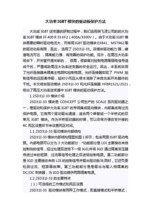
1.1 2SD31I-33驱动模块内部结构2SD31I-33模块内部结构框图如图1所示,包含两路IGBT驱动电路。
内部电路可以分为3大功能部分:*功能部分是LDI主要接收来自控制侧的信号,经过处理后送给下一级IGD;并将IGD通过隔离变压器传送过来的短路、过流等信号处理之后送给控制电路。
第二功能部分是IGD主要接收来自LDI的控制信号并输出驱动脉冲;同时,它还负责检测过流、短路等故障。
第三功能部分是是输出与输入相隔离的DC/DC变换器,为IGD驱动提供两路隔离电源。
1.2 2SD31I-33的主要特点(1)可选择的工作模式和死区设置2SD31I-33驱动模块有两种工作模式,即直接模式和半桥模式,靠模式选择端MOD来决定。
IGBT驱动的解决方案

Special prize from ABB Switzerland
Concept 产品介绍
Scale Driver Scale HVI Driver Standard Driver
Scale Driver 简介
● 电源电压+15V, ● 输入信号 +5V...+15V (可编程), ● 具有直接和半桥模式可供选择。在半桥模式下, 死区时间可选。 ● 过流保护和短路保护, ● 欠压监 测 ● 内置DC/DC 变换器 ● 使用简便灵活。
5000V 5000V 4000V 4000V 4000V 4000V 4000V 4000V 4000V 4000V 4000V 5000V >50 >50 >50 >50 >50 >50 >50 >50 >50
Fiber Fiber Trafo Trafo Trafo Trafo Trafo Trafo Trafo Trafo Trafo Fiber
>100 >100 >100 >100 >100 >100 >100
Trafo Trafo Trafo Trafo Trafo Trafo
Trafo
Standard Driver 简介
● 电流峰值从+/-1.5A 到+/-15A ● 电源电压+15V, ● 输入信号 +15V, ● 具有直接和半桥模式可供选择。在半桥模式下, 死区时间可选。 ● 过流保护和短路保护, ● 欠压监 测 ● 内置DC/DC 变换器 ● 使用简便灵活。 应用:交通运输,通信,军事
+/-6A +/-6A +/-15A +/-15A +/-15A +/-6A +/-6A
IGBT驱动电路的应用设计详解

IGBT驱动电路的应用设计详解IGBT 驱动电路的应用设计隔离驱动产品大部分是使用光电耦合器来隔离输入的驱动信号和被驱动的绝缘栅,采用厚膜或PCB 工艺支撑,部分阻容元件由引脚接入。
这种产品主要用于IGBT 的驱动,因IGBT 具有电流拖尾效应,所以光耦驱动器无一例外都是负压关断。
下面我们就以M57962L 来为基础设计相关的驱动电路!下当单独用M57962L 来驱动IGBT 时。
有三点是应该考虑的。
首先。
驱动器的最大电流变化率应设置在最小的RG 电阻的限制范围内,因为对许多IGBT 来讲,使用的RG 偏大时,会增大td(on )(导通延迟时间),t d(off)(截止延迟时间),tr(上升时间)和开关损耗,在高频应用(超过5 kHz)时,这种损耗应尽量避免。
另外。
驱动器本身的损耗也必须考虑。
如果驱动器本身损耗过大,会引起驱动器过热,致使其损坏。
最后,当M57962L 被用在驱动大容量的IGBT 时,它的慢关断将会增大损耗。
引起这种现象的原因是通过IGBT 的Gres(反向传输电容)流到M57962L 栅极的电流不能被驱动器吸收。
它的阻抗不是足够低,这种慢关断时间将变得更慢和要求更大的缓冲电容器应用M57962L 设计的驱动电路如下电路说明:电源去耦电容C2 ~C7 采用铝电解电容器,容量为100 uF/50 V,R1 阻值取1 kΩ,R2 阻值取1.5kΩ,R3 取5.1 kΩ,电源采用正负l5 V 电源模块分别接到M57962L 的4 脚与6 脚,逻辑控制信号IN 经l3 脚输入驱动器M57962L。
双向稳压管Z1 选择为9.1 V,Z2 为18V,Z3 为30 V,防止IGBT 的栅极、发射极击穿而损坏驱动电路,二极管采用快恢复的FR107 管。
多电路输出的IGBT 驱动设计。
- 1、下载文档前请自行甄别文档内容的完整性,平台不提供额外的编辑、内容补充、找答案等附加服务。
- 2、"仅部分预览"的文档,不可在线预览部分如存在完整性等问题,可反馈申请退款(可完整预览的文档不适用该条件!)。
- 3、如文档侵犯您的权益,请联系客服反馈,我们会尽快为您处理(人工客服工作时间:9:00-18:30)。
Design Considerations in Using the Inverter Gate DriverOptocouplers for Variable Speed Motor Drivesby Jamshed Namdar KhanWhite PaperAbstractInverter Gate Driver optocouplers are ideally suited for IGBT and MOSFET applications for variable speed motor drives. Their high output peak currents coupled with high voltage safety standards certified galvanic insulation, very high com-mon mode noise rejection isolation, solid state device level reliability, and very low power dissipation, makes them in-dispensable inverter gate driver components. The design requirements and power dissipation considerations are made here to ensure that appropriate gate driver optocouplers are selected to match the inverters’ gate charge and power requirements.UPS – Uninterruptible power supplyDTI – Distance through insulationMTTF – Mean time to failureVSD – Variable speed motor drivesUVLO – Under-voltage lockout protectionIntroductionGate driver optocouplers are now commonly used for high power inverter (IGBT or MOSFET) applications such as: motor control, UPS, switching power supplies, high intensity lamp ballast, and induction heating. These inverter gate driver optocouplers have become a component of choice by design engineers because of the many fundamental and key advantages they provide over competing gate driver technologies. The advantages offered by these optocouplers include:1. High Voltage Galvanic Insulation: (reinforced insulation levels) for safety and protection, that includes either the oneminute momentary withstand capability as certified through the UL1577 or the continuous working voltages as certified through IEC60747-5-2 optocoupler safety standards.These levels include up-to 5000 Vrms/1 minute and 1414 Vpk (1000 Vrms or 1000 Vdc) working voltages, depending on the gate driver package selected.2. Noise isolation: Ultra high common mode (dv/dt) noise rejection (CMR) at high common mode Voltages (V CM), up to40 kV/μsec at V CM=1500V are now available.3. Provide safety standards mandated physical spacing such as creepage distances and clearance distances. Somestandards require an internal clearances which is also known as DTI.4. Variable speed data rate capability from DC levels up to the maximum guaranteed speeds.5. Very low detector power dissipation which helps in ease-of-design for providing isolated bootstrapped powersupplies or switching power supplies.6. Solid state reliability levels and very large MTTF.7. Low input drive current or low input power requirements.8. Small footprint area and package sizes (standard 300 mil DIPs), SO-16 or SO-8 packages. Dual gate driver optocouplersare also available.9. Simplicity, ease-of-use, and very few external components required.10. Relatively low cost.Dimensioning the Gate Driver Optocouplers for an IGBT or MOSFETFigure 1 is a typical three phase induction motor (assumed in vector control mode). The six hex-bridge IGBT can be driven with a transformer gate drive, a discrete gate current amplifier drive, an integrated high voltage HVIC gate drive, or an optocoupler gate drive.The primary emphasis here is optocoupler gate drivers for IGBT or MOSFET applications.In selecting a particular inverter gate driver optocoupler, the questions that need to be addressed are:• How much power is dissipated in the output of the gate driver?• How much peak current does an IGBT require for proper switching characteristics?• How much power is delivered to the IGBT gate?• How does one determining what the IGBT gate charge Qg is?• What gate resistor value to pick?• How do you successfully dimension the gate driver?Figure 1. Three phase induction motor with Optocoupler Gate DriversAnalog optocouplers are also available for current sensing and fault detection, gate driver optocouplers for inverter gate driver applications, and digital optocouplers for digital data communications such as DeviceNet, Profibus, RS-485, RS-422, Rs-232, Controller Area Network (CAN), etc.The above advantages are the key reasons for using the gate driver optocouplers for VSD. The VSD ultimately translates into more efficient drives which result in significant power and cost savings. This is primarily due to the power con-sumed by a motor is proportional to the cube of its speed. If the speed of the motor could be more carefully controlled to perform a certain processes more efficiently, then this results in significant energy saving over the life of operation. It is for this reason that VSD is now the most popular application area for consumer home appliances such as washing machines, refrigerators, air-conditioners, fans, mixers, and blenders.The primary focus of this paper is in using the gate driver optocouplers for inverter applications in VSD. These same gate driver optocouplers can also be used in converter applications, such as boost or buck converters, switching power sup-plies, UPS applications, induction heating, electric arc-welders, etc.Figure 2 shows Avago’s ACPL-3130 optocoupler gate driver configured with dual supplies, VCC and VEE . The negative supply VEE is used to provide a reverse gate-emitter voltage or negative gate voltage for a quicker or sharper turn-off of the IGBT, when the output of the gate driver is in the low state.Figure 2. Optically Isolated Gate Driver Using the ACPL-3130 with Negative Gate Voltage (V EE) for Faster IGBT turn-OFF Requirements1. How much total power is dissipated in the optocoupler gate driver? Use the following equation to find the answer.P TOTAL (optocoupler) = (D × I F × V F)+D × Ibias(ON)×(V CC +V EE)+(1-D)×Ibias(OFF) × (V CC + V EE)+ P O(switching)Where:D = duty cycleI F = input drive current of the LED of the optocoupler,V F = LED forward voltageIbias(ON) = is the quiescent supply (V CC+V EE) current in the output high state of the optocoupler (i.e. I CCH parameter in the data sheet)Ibias(OFF) = is the quiescent supply (V CC+V EE) current in the output low state of the optocoupler, (i.e. I CCL parameter in the data sheet)P O (switching) = is the power dissipated in the output pin of the optocoupler and is a function of the switching frequency and energy (E) supplied to the gate of the IGBTP TOTAL(optocoupler) = Power dissipated in the optocoupler2. The second question to address is the output frequency (f SW) dependent output power P O(switching) dissipated inthe output pin of the optocoupler:P O(switching) = E(switching)×f SW(switching)Since the energy stored in the gate capacitance of the IGBT is also the energy supplied by the output of the optocoupler to the IGBT gate capacitance:E(switching) = ½(CV2)Where:C = gate capacitance of the IGBTV = output high voltage of the optocoupler gate driver. Is proportional to the power supply voltage, in this case: (V CC + V EE)When the output of the optocoupler is in the high state (Voh), it can be shown that the energy supplied by the gate driver optocoupler to the IGBT is:E(switching)=½[(QgV CC) + CgeV EE2 ]When the gate driver output is high, the power delivered to the gate of the IGBT from Equation 2 is: Po(Voh)=PO(switching)=E(switching)×f SW(switching) = E×f sw=(f sw/2)×[(QgV CC)+CgeV EE2 ] When the output of the gate driver optocoupler is in the low state, an equal amount of energy must be removed from the gate (conservation of energy principle):Po(vol)=Po(switching)= (f sw /2)×[(QgV CC)+CgeV EE2]3. How much of this power is dissipated in the optocoupler output?The output resistance R(on) of the optocoupler is in series with the Rg(ext) and Rg(int) of the IGBT. Most high performance Avago gate driver optocouplers have bipolar triple Darlington pull-up stage, and MOSFET output pull-down stage.For the MOS Pull-down output stage, when the gate driver is sinking the current:Po(vol)= [Ron(vol) / (Ron(vol)+Rg(ext)+Rg(int))]×(fsw/2)×[(QgV CC)+CgeV EE2]For the triple darlington pull-up stage, when the driver is sourcing current:Po(voh)=[Ron(voh) / (Ron(voh)+Rg(ext)+Rg(int))]×(fsw/2)×[(QgV CC)+CgeV EE2]Considering the duty cycle, the switching power dissipation in the output of the gate driver optocoupler as P(sw): Po(vol)=(1-D)×[Ron(vol) / (Ron(vol)+Rg(ext)+Rg(int))]×(f sw/2)×[(QgV CC)+CgeV EE2]Po(voh)=D × [Ron(voh) / (Ron(voh)+Rg(ext)+Rg(int))]×(f sw/2)×[(QgV CC)+CgeV EE2]Where:Ron(vol) = output resistance of the optocoupler in the output low stateRon(voh) = output resistance of the optocoupler in the output high stateRg(ext) = the external gate resistor at the output of the optocoupler to limit the peak current to the gate of IGBT Rg(int) = the internal gate resistance of the IGBTD = duty cycle between (0 to 1)Qg = total gate charge of the IGBT at the specified gate voltagefsw=switching frequencyIf we assume that the Rg(int) of the IGBT can be neglected, and Ron(vol) is approximately equal to Ron(voh), then the power dissipation formulas can be simplified as:Po(switching)=Pon(vol)+Pon(voh)=[Ron / (Ron+Rg(ext)]×(fsw)×[(QgV CC)+CgeV EE2]A good approximation for the Ron(oh) and Ron(ol) of Avago’s triple Darlington output-high and MOSFET output-low stage gate driver optocouplers is approximately 1.5ohms. The total power dissipated in the optocoupler package is: P total (optocoupler)=(D×I F×V F)+D×Ibias(ON)×(V CC +V EE)+ (1-D)×(Ibias(OFF) ×(V CC+V EE)+P O(switching)Where Po(switching) is now identified:Po(switching)=Pon(vol)+Pon(voh)=[Ron/(Ron+Rg(ext)]×(fsw)×[(QgV CC)+CgeV EE2]4. Sometimes, it is useful to calculate energy supplied to the output of the optocoupler per cycle, which is defined as:Po(switching)/fsw =(Pon(ol)+Pon(oh) ) / fsw=[Ron(oh) / (Ron(oh)+Rg(ext)×[(QgVCC)+CgeV EE2 ]5. The output peak current supplied to the gate of the IGBT by the gate driver optocoupler is:I OH(peak)=[V OH - V EE ] / Rg(ext)Where V OH = V CC – 2V (2V is typical output high saturation voltage and V EE is the negative gate voltage, typically proportioned at V EE = -5V )6. The turn-ON time, td(on) of the IGBT can be calculated as:td(on) =Qg / IpeakWhere Qg is the total gate charge that can be picked readily from the IGBT data sheets, as depicted in the gate voltage vs. gate charge shown in Figure 3.gate charge: Qgg a t e -e m i t t e r v o l t a g e : V g ec o l l e c t o r -e m i t t e r v o l t a g e : V ceFigure 3. IGBT Vge (gate-emitter) Voltage vs. Gate Charge (Qg) CurvesShort Circuit Current Faults and IGBT De-Saturation DetectionAvago’s high performance gate driver optocouplers such as the HCPL-316J, ACPL-332J, and ACPL-331J provide critical safety functions such as the de-saturation fault detection and under-voltage lockout protection (UVLO). The de-satu-ration fault detection circuit provides protection for the power semiconductor switches against short circuit current events which may lead to the destruction of these power switches. These short circuit current faults can usually be at-tributed to phase current and/or rail supply short circuits due to user misconnect or bad wiring, control signal failures due to noise, computational errors, or overload conditions.The IGBT collector-emitter voltage, VCESAT, is monitored by the DESAT pin of the gate driver optocoupler (pins 14 and 16 of Figure 4).When there is a short circuit in an application, and a high current flows through an IGBT, the IGBT will go out of satura-tion mode and its V CESAT voltage will increase. A fault is detected by the optocoupler gate driver (while the IGBT is ON) once this V CESAT voltage goes above the internal de-saturation fault detection threshold voltage (which is typically 6.5V for the ACPL-332J). The DESAT detection circuit is disabled when the gate driver optocoupler output voltage is in the low state. This fault detection triggers two events:1. Output (Vout) of the optocoupler gate driver is slowly brought low in order to “softly” turn off the IGBT and prevent large di/dt induced voltage spikes.2. An internal optically isolated feedback channel is activated, which brings the Fault output low for the purpose of notifying the micro-controller of the fault condition. At this point, the microcontroller must take appropriate action to shutdown or reset the motor drive.The DESAT fault detection circuitry should remain disabled for a short time following the turn-on of the IGBT to allow the collector voltage V CE to fall below the DESAT threshold. The time period, called the DESAT blanking time, ensures that there is no nuisance fault tripping during the IGBT turn-on. This time also represents the time it takes for the driver to go to a fault condition. The blanking time is controlled by the internal DESAT current source, I CHG of 250µA (typical), the DESAT threshold voltage, V DESAT (6.5V typical), and the external blank capacitor, C BLANK .HVDCACPL-332JFigure 4. Recommended Application Circuit with Desaturation Detection Using ACPL-332J or ACPL-331J Gate Driver OptocouplersFigure 5. Desaturation Fault Detection Circuit Using the HCPL-316JThe blanking time is determined by:I C=C×(∆V / ∆T)t BLANK= (C BLANK×V DESAT) / I CHGThe recommended value for the C BLANK is 100 pF which gives a blanking time (t BLANK) of 2.7µs (Condition I CHG = 240µA (typical), V DESAT = 6.5V (typical); page 8 of ACPL-332J datasheet AV02-0120EN-May 7, 2007).The DESAT detection threshold voltage of 6.5V (typical) can be reduced by placing a string of DESAT diodes in series or by placing a low voltage zener diode in series.For the string of DESAT diode method:V DESAT (NEW THRESOLD) = (6.5 -n×V F)For the DESAT diode with the Zener Diode method:V DESAT (NEW THRESOLD) = (6.5 -V F –V Z)Where n is the number of DESAT diodes, V Z is the zener voltage value, and V F is the forward voltage of the DESAT diode. This allows a designer to conveniently select an appropriate DESAT detection threshold voltage.Note the “blanking capacitor charging current” parameter (page 9 of the data sheet for the HCPL-316J optocoupler gate driver) indicated in Table 1.Table 1. Blanking Capacitor Charging Current for the HCPL-316J Gate DriverBlanking Capacitor Charging Current, ICHG Minimum Typical Maximum Units130250330µACalculate the blanking time based the blanking capacitor charging current as shown in Table 1 for the HCPL-316J gate driver optocoupler using the below equations.I CHG = C×(∆V / ∆t)Transposing and calculating for the blanking time, ∆t, with the internal typical de-saturation voltage detection level of 7V (for the HCPL-316J or the HCPL-332J) we find:∆t (maximum)=(100 pF×7V ) / 130µA=5.38µsec∆t (typical)=(100 pF×7V) / 250µA=2.80µsec∆t (minimum)=(100 pF×7V) / 330µA=2.12µsecFor most applications the above indicated blanking time variation would be acceptable. To minimize the blanking time variation, an external blanking circuit approach is shown in Figure 6.Figure 6 shows a concept for an external blanking circuit. This method uses one additional external resistor, RB, connect-ed from the output to the DESAT pin 14 of the HCPL-316J gate driver. This allows an additional blanking capacitor charg-ing current component from the output of the gate driver optocoupler through RB and this adds to the internal current source of the gate driver optocoupler. This higher external blanking capacitor charging current allows a designer greater flexibility in choosing both an appropriate value of the blanking capacitor, C B, and an appropriate current through the choice of the external resistor R B. By adjusting the capacitance of the blanking capacitor C B and the additional external blanking current through R B, a designer can set a specific precise blanking time.HCPL-316JFigure 6. External Blanking Circuit Approach Using Resistor (R B ) and Capacitor (C B )The voltage on the blanking capacitor can be written as: V C (t)=V I – V f [1-e (-t /RC)] Where: V EE = -9V V CC2 = 17V R B = 1000 kΩC B = 4700 pF (blanking capacitor) At t =0 V C (0) = VI = -9V At t = ∞V C (∞) = VI + Vf = -9V + 26V = 17V This can be written as:V C (t)=7V= -9V + 26[1– e (-t/RC) ] or e (-t/RC) =[1 – 16/26] ( -t blank /RC)=ln (0.3846)Calculating for the blanking time, t(blank), with R B = 1000Ω and C B = 4700pF: t(blank)= - R B C B ln(0.3846)=4.5µsecThis external blanking time (t blank ) calculation shows that by introducing an additional external blanking capacitor charging current (I CHG ) through a resistor R B , allows one to have a greater control over the blanking time. Figure 7 shows the fault detection and rest timing waveforms of the HCPL-316J gate driver optocoupler.Discharging the IGBT gate through Negative Gate Bias or Active Miller ClampUnlike a MOSFET, an IGBT normally requires a negative gate voltage to minimize the switching losses due to the slow “turn-off tail current”. The negative gate voltage helps to quickly reverse bias of the gate emitter voltage during the turn-OFF and minimize the switching losses. An additional benefit of the negative gate bias voltage is to improve the dv/dt noise immunity of the IGBT. The gate to collector “Miller capacitance”, can induce a false turn-ON due to high collector-to-emitter dv/dt induced during the switching sequence. Most Avago gate driver optocouplers (such as the HCPL-316J, HCPL-3130, and HCPL-3120) can be operated either with a single supply or with dual supplies if a negative gate drive is desired for a quick turn-OFF of the IGBT as shown in Figures 2 and 6.To avoid the necessity of a dual power supply to provide the “negative gate drive” for a fast turn-off of the IGBT, another method employed by some Avago gate drivers is to provide an alternative low impedance path with a high sink current capability called an Active Miller clamp (The Active Miller clamp feature is available in gate drivers such as the ACPL-332J and the ACPL-331J). Figure 8 is the ACPL-332J internal block diagram, showing the additional power FET transistor that provides the shunt low impedance path for gate discharge, and also clamps the gate of the IGBT at a low voltage during the entire turn-OFF time.The Pin (10) of the ACPL-332J and ACPL-331J is the Active Miller clamp pin. An internal high power MOSFET transistor offers the low impedance path for the gate turn-off and discharge current. This “switch” shorts the gate-emitter voltage of the IGBT after the threshold level is reached. The currents associated with the Miller capacitance are also shunted by this switch instead of flowing through the output (Vout) of the gate driver optocoupler (Pin 11).During the turn-OFF, the gate voltage of the IGBT is monitored and clamp output is activated when the gate voltage goes below 2V (relative to V EE, pins 9 and 12). The clamp voltage is typically V OL+ 2.5V for a Miller current up to 1.1A. The Active Miller clamp function is disabled when the LED input is triggered again, and the output of the gate driver optocoupler is in the output high state.ConclusionIn this paper we have considered the inverter gate driver optocoupler for variable speed three phase induction motors. Gate driver optocouplers provide some key and fundamental features that are required for high power bus applications using IGBTs or MOSFETs. These features include high insulation voltages for galvanic safety isolation, high output peak currents, and ultra-high dv/dt common mode noise immunity (CMR). Safety features include de-saturation fault detec-tion, under-voltage lockout, optically isolated fault-status feedback for the micro-controller, and soft output turn-off to prevent high di/dt induced voltage spikes. To minimize the IGBT switching power losses, these gate driver optocouplers also provide ability for a negative gate bias voltage through the use of dual power supplies. Other gate drivers provide Active Miller clamps which preclude the need for the negative gate supply voltage.Dynamic maximum power dissipation equations were derived for the gate driver optocoupler as a function of the gate resistor, power supply levels, and switching frequency.Figure 8. ACPL-332J block Diagram, with Active Miller Clamp for Fast Gate Turn-OFF of an IGBT or MOSFET(Pin 10)For product information and a complete list of distributors, please go to our web site: Avago, Avago Technologies, and the A logo are trademarks of Avago Technologies, Limited in the United States and other countries.Data subject to change. Copyright © 2007 Avago Technologies Limited. All rights reserved. AV02-0803EN - November 19, 2007References[1] Muhammad H. Rashid, Editor, “ Power Electronics Handbook,” 2nd Edition, Academic Press, San-Diego, 2007.[2] Muhammad H. Rashid, “Power Electronics: Circuits, Devices, and Applications,” 2nd Edition, Prentice-Hall, New Jersey, 1993.[3] Jamshed Namdar Khan, “Optocouplers for Variable Speed Motor Control Electronics in Consumer Home Appliances,” Proceedings of the 52nd International Appliance Technical Conference (IATC), pp. 256-285, 2001.[4] Jamshed Namdar Khan, “Using Hermetic Optocouplers in Military and Space Electronics,” 5th Annual International Conference, Commercialization of Military and Space Electronics, 2001[5] Jamshed Namdar Khan, “Regulatory Guide to Isolation Circuits,” Hewlett-Packard publication number 5965-5853E, January 1, 1997, and Avago Technologies Publication Number 5989-2937EN, July 17, 2007.[6] Malcolm Barnes, “Practical Variable Speed Drives and Power Electronics,” Newnes, Oxford, 2003.[7] “Desaturation Fault Detection,” AN 5324, Avago Technologies, 2007[8] “Soft Turn-Off Feature,” AN 5315, Avago Technologies, 2007[9] “ Active Miller Clamp,” AN 5314, Avago Technologies, 2007[10] Yeo Siok Been, Jamshed Namdar Khan, and Derek Chng Peng Hui, “Designing Medical Devices for Isolation and Safety,” EDN (Electronic Design, Strategy, News), pp. 75-78, May 24, 2007. This paper was first presented at the Power Electronics Technology Conference 2007.。