5082-5701-KD000中文资料
上海欧际 液压软管 样本
a、N-M、N-G、N-R、N-NPT、N-φ、N-K 这里的 N(NIPPLE)表示外螺纹接头,M、G、 R、NPT 表示螺纹形式,φ表示与钢管焊接,K 表示卡套连接。 b、90E-R、45E-G 中的 90E(ELBOW)表示 90°弯头,45E(ELBOW)表示 45°弯头。
6
c、6F-C、3F-E、F-H、W-φ中的 6F(FLANGE)-C(CONNECT)表示 6000 系列法兰连接, 3F(FLANGE)-E(ELBOW)表示 3000 系列 90°法兰连接,F(FLANGE)-H(HALF) 表示半片法兰连接,W(WELD)-φ表示成对法兰焊连接。
目录
4
一、选 用 说 明
1、选择原则: a、根据使用条件(压力、介质、温度、弯曲半径等)选用软管; b、根据流量确定软管通径; c、根据通径、设备结构和连接方式确定两端软管接头型式,并选择过渡接头; d、确定软管长度; e、如两端接头都为弯头形式,需确定其在圆周方向的装配角度;
图 1 软管总成装配角度 f、根据环境温度和摩擦状况判断是否需加保护层或耐磨表皮。
公司于 2004 年 8 月通过了 ISO9001-2000 质量体系认证,全体员工始终贯彻 “科技先导、开拓创新、质量第一、诚信为本”的欧际精神,精诚合作,共创企 业辉煌,共图发展大计。公司拥有先进的数控车床、精模锻设备、中频电炉、喷 丸机及检测设备 258 台(套),并实行计算机网络信息管理。
公司全系列生产符合 ISO、DIN、JIS 标准的管路附件。符合 GB、GB/T、JB/ZQ、 JB、JB/T 等国家或行业标准的系列管路附件,旋转接头、快换接头、不锈钢金属 软管总成、液压胶管总成、铠装液压胶管总成、干稀油润滑设备。设计生产各种 非标的管路附件、液压系统等。
甘露醇氯化钠琼脂培养基产品说明书

化学品安全技术说明书第一部分化学品及企业标识产品中文名称:甘露醇氯化钠琼脂培养基产品英文名称:Mannitol Salt Agar产品编号:024022企业名称:广东环凯微生物科技有限公司地址:广东省广州市黄埔区广州开发区科学城神舟路788号邮编:510663公司网址电子邮件地址:*********************传真号码:************销售热线:************-8602技术热线:************-8877/8876推荐用途和限制用途:生化研究/分析第二部分危险性概述GSH危害性类别非危险物质或混合物GSH标签要素非危险物质或混合物其它危害(健康危害、环境危害)未见报道第三部分成分/组成信息混合物化学品成分:参考培养基使用说明。
有害物质成分:无第四部分急救措施一般信息:无特殊的措施要求。
皮肤接触:立即用清水彻底清洗。
眼睛接触:立即提起眼睑,用大量流动清水冲洗15min。
如不适就医。
吸入:如果吸入,将人员移动到新鲜空气处,如果没有呼吸,进行人工呼吸操作,并联系医生。
食入:如误食,用水冲洗口腔,如不适就医。
就医信息:出示产品使用说明或者此MSDS。
第六部分 泄露应急处理个人防护: 穿个人实验服,佩戴手套和口罩,避免吸入干粉。
环境保护措施: 用湿布和地拖擦拭干净。
清洁/收集措施: 保持干燥。
迅速清洗弄脏的区域。
第七部分 操作处置与储存安全操作注意事项: 防止粉尘扬起,应提供通风设备。
储存注意事项: 贮存于避光、干燥处,用后立即旋紧瓶盖。
第八部分 接触控制/个人防护职业接触限值 没有已知的国家规定的暴露极限。
工程控制: 提供安全淋浴和洗眼设备个人保护措施 呼吸系统防护: 在通风橱里称取产品,佩戴口罩。
眼睛防护: 佩戴安全眼镜。
身体防护: 穿实验室服。
手防护: 戴防化学品手套。
其他防护: 常规的工业卫生操作,工作后及时清洗双手。
第九部分 理化特性外观: 粉末 pH 值: 无相关资料 颜色: 淡黄色 气味: 特征性 熔点: 无数据资料 沸点: 无数据资料 燃点: 无数据资料闪点:无数据资料爆炸限度 下限: 无数据资料 上限: 无数据资料 热分解: 无数据资料溶解性: 按产品使用说明上的用量比例加蒸馏水,加热煮沸至完全溶解,溶液呈红色澄清无沉淀。
5082-2800中文资料

Schottky Barrier Diodes for General Purpose ApplicationsTechnical DataFeatures• Low Turn-On VoltageAs Low as 0.34 V at 1 mA• Pico Second Switching Speed • High Breakdown VoltageUp to 70 V• Matched Characteristics AvailableDescription/Applications The 1N5711, 1N5712, 5082-2800/ 10/11 are passivated Schottky barrier diodes which use a patented “guard ring” design to achieve a high breakdown voltage. Packaged in a low cost glass package, they are well suited for high level detecting, mixing, switching, gating, log or A-D converting, video detecting, frequency discriminating, sampling, and wave shaping.The 5082-2835 is a passivatedSchottky diode in a low cost glasspackage. It is optimized for lowturn-on voltage. The 5082-2835 isparticularly well suited for theUHF mixing needs of the CATVmarketplace.The 5082-2300 Series and5082-2900 devices are unpas-sivated Schottky diodes in a glasspackage. These diodes haveextremely low 1/f noise and areideal for low noise mixing, andhigh sensitivity detecting. Theyare particularly well suited for usein Doppler or narrow band videoreceivers.1N57111N57125082-2300 Series5082-2800 Series5082-2900DIMENSIONS IN MILLIMETERS AND (INCHES).Outline 15Maximum RatingsJunction Operating and Storage Temperature Range5082-2303, -2900.................................................................-60°C to +100°C 1N5711, 1N5712, 5082-2800/10/11....................................-65°C to +200°C 5082-2835............................................................................-60°C to +150°C DC Power Dissipation(Measured in an infinite heat sink at T CASE = 25°C)Derate linearly to zero at maximum rated temperature5082-2303, -2900..............................................................................100 mW 1N5711, 1N5712, 5082-2800/10/11.................................................250 mW 5082-2835.........................................................................................150 mW Peak Inverse Voltage.................................................................................V BRPackage CharacteristicsOutline 15Lead Material........................................................................................DumetLead Finish..............................................................................95-5% Tin-LeadMax. Soldering Temperature................................................260°C for 5 secMin. Lead Strength....................................................................4 pounds pullTypical Package Inductance1N5711, 1N5712:................................................................................2.0 nH2800 Series:........................................................................................2.0 nH2300 Series, 2900:..............................................................................3.0 nHTypical Package Capacitance1N5711, 1N5712:................................................................................0.2 pF2800 Series:........................................................................................0.2 pF2300 Series, 2900:............................................................................0.07 pFThe leads on the Outline 15 package should be restricted so that thebend starts at least 1/16 inch from the glass body.Outline 15 diodes are available on tape and reel. The tape and reelspecification is patterned after RS-296-D.Electrical Specifications at T= 25°CAGeneral Purpose DiodesMin.Max.V F = 1 V Max.Max.Max.Breakdown Forward at Forward Reverse Leakage Capaci-Part Package Voltage Voltage Current Current tance Number Outline V BR (V)V F (mV)I F (mA)I R (nA) at V R (V)C T (pF) 5082-280015704101520050 2.0 1N571115704101520050 2.0 5082-281015204103510015 1.2 1N571215205503515016 1.2 5082-28111515410201008 1.2 5082-2835158*34010*1001 1.0 Test I R = 10 µA I F = 1 mA*V F = 0.45 V V R = 0 V Conditions*I R = 100 µA f =1.0 MHz Note: Effective Carrier Lifetime (τ) for all these diodes is 100 ps maximum measured with Krakauer method at 5 mA except for 5082-2835 which is measured at 20 mA.Low 1/f (Flicker) Noise DiodesMin.Max.V F = 1 V Max.Max.Max.Part Breakdown Forward at Forward Reverse Leakage Capaci-Number Package Voltage Voltage Current Current tance 5082-Outline V BR (V)V F (mV)I F (mA)I R (nA) at V R (V)C T (pF) 230315204003550015 1.0 29001510400201005 1.2 Test I R = 10 µA I F = 1 mA V R = 0 V Conditions f =1.0 MHzNote: Effective Carrier Lifetime (τ) for all these diodes is 100 ps maximum measured with Krakauer method at 20 mA.Matched Pairs and QuadsBasic Matched MatchedPart Number Pair Quad Batch5082-Unconnected Unconnected Matched[1]Test Conditions2900∆VF at IF= 1.0, 10 mA28005082-28045082-2805∆V F at I F = 0.5, 5 mA ∆V F = 20 mV∆V F = 20 mV*I F = 10 mA∆C O at f = 1.0 MHz28115082-2826∆VF at IF= 10 mA∆V F = 10 mV∆C O at f = 1.0 MHz ∆C O = 0.1 pF28355082-2080∆VF at IF=10 mA∆V F = 10 mV∆C O at f = 1.0 MHz∆C O = 0.1 pFNote:1. Batch matched devices have a minimum batch size of 50 devices.SPICE ParametersParameter Units5082-28005082-28105082-28115082-28355082-23035082-2900B V V75251892510C J0pF 1.60.8 1.00.70.7 1.1E G eV0.690.690.690.690.690.69I BV A10E-510E-510E-510E-510E-510E-5I S A 2.2 x 10E-9 1.1 x 10E-90.3 x 10E-8 2.2 x 10E-87 x 1.0E-910E-8N 1.08 1.08 1.08 1.08 1.08 1.08 R SΩ25101051015 P B V0.60.60.60.560.640.64 PT222222 M0.50.50.50.50.50.5Typical ParametersV F – FORWARD VOLTAGE (V)Figure 1. I-V Curve Showing Typical Temperature Variation for 5082-2300 Series and 5082-2900 Schottky Diodes.1001010.10.01I F - F O R W A R D C U R R E N T (m A )V BR (V)Figure 2. 5082-2300 Series Typical Reverse Current vs. Reverse Voltage at Various Temperatures.10.0001,000100101I R (n A )051015100755025T A = 25°CI F - FORWARD CURRENT (mA)Figure 3. 5082-2300 Series and 5082-2900 Typical Dynamic Resistance (R D ) vs. Forward Current (I F ).100010010R D - D Y N A M I C R E S I S T AN C E (Ω)0.01010100V R - REVERSE VOLTAGE (V)Figure 4. 5082-2300 and 5082-2900 Typical Capacitance vs. Reverse Voltage.1.21.00.80.60.40.20C T - C A P A C I T A N C E (p F )048121620V F - FORWARD VOLTAGE (V)Figure 5. I-V Curve Showing Typical Temperature Variation for 5082-2800 or 1N5711 Schottky Diodes.5010510.50.10.050.01I F - F O R W A R D C U R R E N T (m A )00.20.40.60.8 1.0 1.2V R - REVERSE VOLTAGE (V)Figure 6. (5082-2800 OR 1N5711) Typical Variation of Reverse Current (I R ) vs. Reverse Voltage (V R ) at Various Temperatures.100,00010,0001000100101I R - R E V E R S E C U R R E N T (n A )0.20.40.60.81.01.2V R - REVERSE VOLTAGE (V)Figure 7. (5082-2800 or 1N5711)Typical Capacitance (C T ) vs. Reverse Voltage (V R ).12.01.51.00.50C T - C A P A C I T A N C E (p F )010********V F - FORWARD VOLTAGE (V)Figure 8. I-V Curve Showing Typical Temperature Variation for the 5082-2810 or 1N5712 Schottky Diode.100101.00.10.01I F - F O R W A R D C U R R E N T (m A )V R - REVERSE VOLTAGE (V)Figure 9. (5082-2810 or IN5712)Typical Variation of Reverse Current (I R ) vs. Reverse Voltage (V R ) at Various Temperatures.10,0001000100101.0I R - R E V E R S E C U R R E N T (n A )Typical Parameters, continuedV F - FORWARD VOLTAGE (V)Figure 10. I-V Curve Showing Typical Temperature Variation for the 5082-2811 Schottky Diode.100101.00.10.01I F - F O R W A R D C U R R E N T (m A )0.40.20.60.81.01.2V R - REVERSE VOLTAGE (V)Figure 11. (5082-2811) Typical Variation of Reverse Current (I R ) vs. Reverse Voltage (V R ) at Various Temperatures.100,00010,0001000100101I R - R E V E R S E C U R R E N T (n A )0510********V F - FORWARD VOLTAGE (V)Figure 12. I-V Curve Showing Typical Temperature Variations for 5082-2835 Schottky Diode.100101.00.10.01I F - F O R W A R D C U R R E N T (m A )00.20.40.60.8 1.0 1.2V R - REVERSE VOLTAGE (V)Figure 13. (5082-2835) Typical Variation of Reverse Current (I R ) vs. Reverse Voltage (V R ) at Various Temperatures.100,00010,0001000100101I R - R E V E R S E C U R R E N T (n A )0123456V R - REVERSE VOLTAGE (V)Figure 14. Typical Capacitance (C T ) vs. Reverse Voltage (V R ).C T - C A P A C I T A N C E (p F )0246810I F - FORWARD CURRENT (mA)Figure 15. Typical Dynamic Resistance (R D ) vs. Forward Current (I F ).1000100101R D - D Y N A M I C R E S I S T A N C E (Ω)Diode Package Marking1N5xxx5082-xxxxwould be marked:1Nx xxxxx xxYWW YWWwhere xxxx are the last four digits of the 1Nxxxx or the 5082-xxxx partnumber. Y is the last digit of the calendar year. WW is the work week ofmanufacture.Examples of diodes manufactured during workweek45 of 1999:1N57125082-3080would be marked:1N53071280945945Data subject to change.Copyright © 1999 Agilent TechnologiesObsoletes 5968-4304E5968-7181E (11/99)。
DIN 53505-2000中文

附录 A
硬度试验方法的适用范围 邵尔 A 依照 DIN 53505 IRHD,低硬度范围 依照 DIN 53519-1,5mm 直径球 IRHD,一般硬度范围 依照 DIN 53519-1,2.5mm 直径球 邵尔 D 依照 DIN 53505 球印硬度 依照 DIN EN ISO 2039-1 软←硬度→硬 图 A.1 :硬度试验方法的适用范围 (各方法之间不存在线性关系)
附录 A 中给出了不同的硬度试验方法的适用范围的概述。
第 2 到 5 页继续
标准编号 DIN 53505:2000-08
第2页 DIN 53505:2000-08
2 引用标准
本标准包括了,通过指定日期或未指定日期引用的来自其它出版物的规定。这些参考标准在本文的相应地方被引 用,并且出版物的名称在下面列出。对于指定日期的引用,只有当经过修改或修订而包括在内时,这些出版物的任何 改动或修订才适用于本标准。对于未指定日期的引用,所涉及到的出版物的最新版本适用。
din51220材料试验机的一般技术要求包括检定及校准橡胶的拉伸应力应变特性的测定采用标准试样进行软橡胶的压痕硬度irhd的测定采用小试样进行软橡胶的压痕硬度irhd的测定通过测量橡胶的硬度进行结晶效应的测定橡胶的低温特性的测定原则及试验方法用来自弹性体及塑料上的试验实例进行随机样本的统计评估塑料及硬橡胶借助于硬度计邵尔硬度测定压痕硬度iso868
德国标准
邵尔 A 及邵尔 D 橡胶硬度试验
2000 年 8 月
ICS 83.060
本标准,连同 DIN EN ISO 868 1998 年 1 月版本,取代了 1987 年 6 月版本。
与国际标准化组织(ISO)所发布的标准中的习惯用法一样,自始至终采用逗号作为十进制标记。
常用修饰剂介绍
kh570编辑KH-570硅烷偶联剂,γ-甲基丙烯酰氧基丙基三甲氧基硅烷是一种有机官能团硅烷偶联剂,对于提高玻纤增强和含无机填料的热固性树脂能提高它们的机械电气性能,特别是通过活性游离基反应固化(如不饱和聚酯,聚氨酯和丙烯酸酯)的热塑性树脂的填充,包括聚烯烃和热塑性聚氨酯。
国外对应牌号:A-174(美国联合碳化物公司)KBM-503(日本信越化学工业株式会社)SH-6030(美国道康宁化学公司)三、化学名称:γ-(甲基丙烯酰氧)丙基三甲氧基硅烷四、分子式:CH2=C(CH3)COOC3H6Si(OCH3)3五、典型的物理性质参数标准指标外观微黄色至无色透明液体颜色Pt-Co, ≤ 30密度(ρ 20℃,g/cm3)1.043~1.053折光率(nD 25°C)1.4285 ~1.4310沸点:255℃纯度%, ≥ 97.0溶解性硅烷偶联剂KH-570可溶于甲醇、乙醇、乙丙醇、丙酮、苯、甲苯、二甲苯,水解后在搅拌下可溶于PH=4的水中,水解产生甲醇.六、用途:主要用于改善有机材料和无机材料的粘接性能,特别适用于游离基交联的聚酯橡胶,聚烯烃、聚苯乙烯和在光敏材料中作为助剂。
七CAS NO. : 2530-85-0八特征和用途KH-570硅烷偶联剂的用途:(1)当复合材料用经过与聚酯相容的表面处理剂处理过的玻纤时,能显著提高复合材料的强度,这种表面处理剂通常包括硅烷偶联剂、成膜剂、润滑剂和抗静电剂。
(2)此产品提高填充白碳黑、玻璃、硅酸盐和金属氧化物的聚酯复合材料的干湿态机械强度。
(3)此产品提高许多无机填料填充复合材料的湿态电气性能。
例如:交联聚乙烯和聚氯乙烯。
(4)此产品可与醋酸乙烯和丙烯酸酯或甲基丙烯酸酯单体共聚合成可室温交联固化的。
这些硅烷团化聚合物广泛应用于涂料、胶粘剂和密封胶中。
提供优异的粘接力和耐久力。
一、概述:偶联剂kh570是一类具有两不同性质官能团的物质,它们分子中的一部分官能团可与有机分子反应,另一部分官能团可与无机物表面的吸附水反应,形成牢固的粘合。
ST570技术说明书V1.0

TK000-经典通用宝藏文档
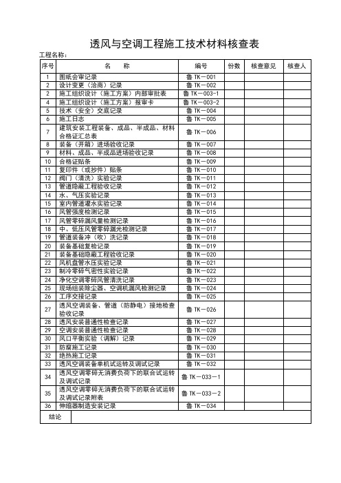
伸缩器制造安装记录
鲁TK-034
结论
总监理工程师签字: 年 月 日
山东省建设工程质量监督总站监制
7
建筑安装工程装备、成品、半成品、材料合格证汇总表
鲁TK-006
8
装备(开箱)进场验收记录
鲁TK-007
9
材料、成品、半成品进场验收记录
鲁TK-008
10
合格证贴条
鲁TK-009
11
复印件(或抄件)贴条
鲁TK-010
12
阀门(清洗)实验记录
鲁TK-011
13
管道隐蔽工程验收记录
鲁TK-012
14
水、气压实验记录
鲁TK-028
30
风口平衡实验(调解)记录
鲁TK-029
31
防腐施工记录
鲁TK-030
32
绝热施工记录
鲁TK-031
33
透风空调装备单机试运转及调试记录
鲁TK-032
34
透风空调零碎无消费负荷下的联合试运转及调试记录
鲁TK-033-1
35
透风空调零碎无消费负荷下的联合试运转及调试记录附表
鲁TK-033-2
鲁TK-021
23
制冷零碎气密性实验记录
鲁TK-022
24
净化空调零碎风管清洗记录
鲁TK-023
25
现场组装除尘器、空调机漏风检测记录
鲁TK-024
26
工序交接记录
鲁TK-025
27
透风空调装备、管道(防静电)接地检查验收记录
鲁TK-026
28
透风安装普通性检查记录
鲁TK-027
29
空调安装普通性检查记录
海德能膜产品技术手册
目录第一章美国海德能公司RO/NF膜产品规格与性能第二章反渗透及纳滤膜应用技术介绍第三章反渗透、纳滤基础知识第四章水化学与水质分析第五章预处理第六章反渗透系统设计第七章反渗透膜的安装及运行第八章污染与清洗第九章RO/NF系统故障诊断和排除第十章海德能公司反渗透膜元件质量保证书第十一章海德能公司退货程序(RGA)第十二章反渗透技术问答第十三章应用技术文献第一章美国海德能公司RO/NF膜产品规格与性能1.1 8英寸膜元件端板新型涡旋切1。
2 流式设计美国海德能公司已于2002年12月12日正式推出针对所有标准的 8 英寸膜元件端板的新型涡旋切流式(以下简称为“切流式”)设计。
这一新的密封支撑/防止膜卷突出设计(ATD)提供了更好的端面接触,使水力负荷分布的更加均匀.新的切流式设计保持了海德能公司产品多孔端板的特点,该端板可以保护膜元件免受因较大颗粒撞击而造成的损坏。
这一特殊的涡旋式图案设计使得穿过膜元件表面的水具有均匀的分布,并可以平衡膜元件外部和中心管的压力。
新的切流式可以很容易地由其象牙色和涡旋式结构辨认,而不同于以前的灰色和直线式。
同时,我们还将介绍新型内连接管,它即适用于新型切流式膜元件,也适用于传统的海德能膜元件.新型内连接管具有很多好处,在负载和操作过程中不会脱离。
新型切流式膜元件完全与工业市场中众多其它的膜元件相兼容。
海德能公司正致力于膜元件内部密封方法的研究,以提供压力容器中膜元件之间密封连接的最大保证。
目前正使用的非切流式膜元件设计可以允许内部和外部的密封。
海德能公司在持续不断地为我们的用户研究和开发创新的、改进性的产品。
新切流设计在保持水通量和脱盐率的一致性及可靠性的基础上提供了附加的益处。
海德能公司正在以改进的设计模式,在无附加成本的情况下,一同既往地生产高质量的膜产品。
技术说明—新型切流式膜元件需使用内连接管- 每支新型切流式膜元件的包装中均装备一支内连接管- SWC 系列内连接管部件号码不同于其它苦咸水反渗透膜产品的内连接管部件号码—新切流式膜元件不能使用外连接管和外连接型端板接头—新型内连接管同时适用于新型切流式和传统膜元件—新切流式设计膜元件与市售的大多数公司的膜元件的连接管和端板接头完全兼容—标准中心管内径为1。
HK-508型铁含量分析仪说明书
京制 01080126 号HK-508型铁含量分析仪使用说明书产品版本:1.0 北京华科仪电力仪表研究所目录一、概述1.1 仪器简介 (1)1.2 显示及操作面板 (1)1.3 工作原理 (2)二、技术指标 (4)三、试剂的制备3.1 显色试剂的制备 (5)3.2 标准储备溶液 (5)四、编程4.1 开机 (6)4.2 程序单元 (6)4.2.1 主菜单 (6)4.2.2 空白校准菜单 (7)4.2.3 曲线校准菜单 (8)4.2.4 参数设置菜单 (9)4.2.5 历史数据菜单 (10)五、仪器的使用5.1 使用条件 (12)5.2 仪器的安装方法 (12)5.3 仪器的校准 (12)5.3.1 曲线校准 (12)5.3.2 空白校准 (15)5.4 水样的测定方法 (15)5.4.1 待测水样的显色 (15)5.4.2 水样的测量 (15)5.5 注意事项 (15)六、仪器的成套性 (17)1一 概述仪器外型为一个密封的金属壳体,坚固防水;显示屏为大屏幕的点阵液晶,中文菜单,易于理 解,操作方便;测量数据为直读式,并可根据需要保存测量值。
其中,键盘功能如下::垂直或水平循环移动光标,选择所需的菜单或参数。
:当参数选定后,可增加参数的数值; 当显示历史数据、对历史数据进行查询时,按此键可显示上页数据。
:当参数选定后,可减小参数的数值。
当显示历史数据、对历史数据进行查询时,按此键可显示下页数据。
:当选定所需的菜单或功能项,按此键可进入该菜单或功能项;:返回上一菜单或上一页。
:排空比色池中的液体,此时测量值不存储。
排液时间设置为 16 秒。
:对测量数值进行存储,同时排空比色池中的液体。
1. 测量数值的存储:仪器具有 6 个存储通道,可将不同水样的测量值存储到所需的通道中。
在测量画面中, 待测量水样的数值显示稳定后,直接用“+”或“-”键改变所需存储的通道,然后按下“存 储”键。
2. 空白校准或曲线校准的存储:空白和曲线校准的时间将直接存储到 6 个通道中,而无需选择存储通道,(这样做的目的 在于可随时了解仪器的校准情况)。
SUN2000-5 8 10KTL-M0系列商品说明书
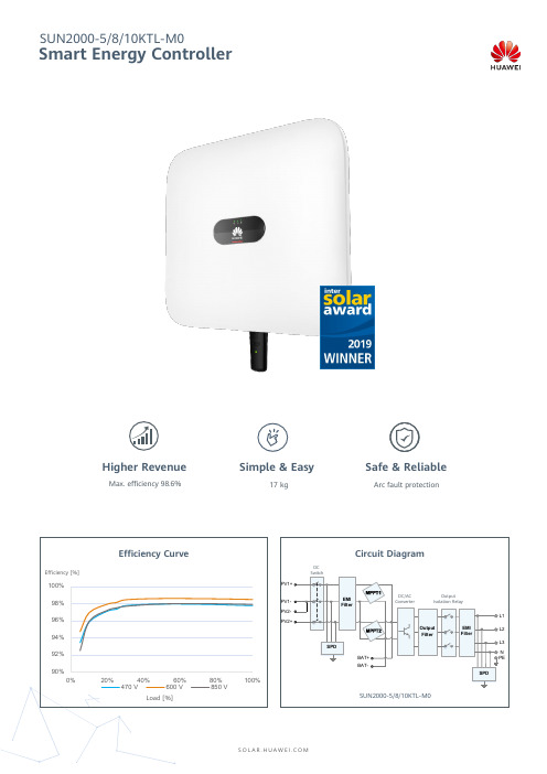
98.6% 98.1%
Recommended max. PV power 1 Max. input voltage 2 Operating voltage range 3 Start-up voltage Rated input voltage Max. input current per MPPT Max. short-circuit current Number of MPP trackers Max. input number per MPP tracker
Efficiency Curve
20%
40%
470 V
60% 600 V
Load [%]
80% 850 V
100%
PV1+
PV1PV2PV2+
Circuit Diagram
DC Switch
EMI Filter
SPD
BAT+ BAT-
DC/AC Converter
Output Isolation Relay
16.9 A
0.8 leading ... 0.8 lagging
≤3%
Input-side disconnection device Anti-Islanding protection DC reverse polarity protection Insulation monitoring DC surge protection AC surge protection Residual current monitoring AC overcurrent protection AC short-circuit protection AC overvoltage protection Ripple receiver control Arc fault protection (AFCI)
Biochrom30氨基酸分析仪

Biochrom 30+特点介绍
氮气保护系统: • 防止缓冲液、衍生试剂被氧化,延长试剂寿
命 • 防止氧气进入缓冲液,导致样品中易氧化组
分被破坏,影响分析结果 • 用而不耗,节约成本 • 氮气过压保护,防止由于氮气阀没有调节好
而引起缓冲液、衍生试剂瓶发生爆炸的危险
Page 17 © DKSH
生理体液j加速分析标准图谱(48种氨基酸 570nm)
Page 28 © DKSH
血浆中游离氨基酸分析— —英国曼彻斯特皇家儿童医院提供
Page 29 © DKSH
苯丙酮尿症中氨基酸分析— —英国曼彻斯特皇家儿童医院提供
Page 30 © DKSH
绿茶中游离氨基酸分析— —英国Biochrom剑桥实验室提供
色谱柱采用惰性PEEK材料,使得每次分析完成后的再生清洗可采用高浓 度氢氧化钠溶液,并可加温至99℃的高温,对于氢氧化钠无法清洗的污 染物,如:高脂、高糖污染物达到很好的分解清洗作用,延长色谱柱使用 寿命。
该仪器色谱柱填料使用安玛西亚生产填料,原安玛西亚公司不但是世界上 最大的填料生产商,而且填料质量在全世界公认是最好的。
是中国市场上唯一获得FDA市场准入许可,并符合联邦药物、食品和化妆 品条款的氨基酸分析仪。
唯一采用陶瓷泵的专用自动氨基酸分析系统,完全避免了传统不锈钢泵头 被含高盐的缓冲液侵蚀的危险,全机流路采用PEEK 惰性材料,使清洗维 护都变得简单。
Page 32 © DKSH
Biochrom 30 +氨基酸技术特点
Page 22 © DKSH
水解蛋白标准分析图谱
Page 23 © DKSH
新的饲料资源-大豆皮 中氨基酸分析
ICS-2000
ICS-2000离子色谱系统操作手册戴安中国有限公司技术服务中心2003.4目录1. 简介﹒﹒﹒﹒﹒﹒﹒﹒﹒﹒﹒﹒﹒ 22.仪器介绍﹒﹒﹒﹒﹒﹒﹒﹒﹒﹒﹒﹒﹒ 63. 操作﹒﹒﹒﹒﹒﹒﹒﹒﹒﹒﹒﹒﹒254. 故障指南﹒﹒﹒﹒﹒﹒﹒﹒﹒﹒﹒﹒﹒315. 维修﹒﹒﹒﹒﹒﹒﹒﹒﹒﹒﹒﹒﹒39 附录A 技术指标﹒﹒﹒﹒﹒﹒﹒﹒﹒﹒﹒﹒﹒64 附录B 安装﹒﹒﹒﹒﹒﹒﹒﹒﹒﹒﹒﹒﹒67 附录C 触摸屏幕﹒﹒﹒﹒﹒﹒﹒﹒﹒﹒﹒﹒﹒78 附录D常见问题﹒﹒﹒﹒﹒﹒﹒﹒﹒﹒﹒﹒﹒911. 简介1.1离子色谱ICS-2000离子色谱系统可以进行抑制型或非抑制型电导检测,它由淋洗液、高压泵、进样阀、保护柱/分离柱、抑制器、电导池和数据处理系统组成。
首先分析已知组成和浓度的标准样品溶液,由数据处理系统生成校正曲线,再分析经过必要前处理的样品溶液,数据处理系统将其结果与先前生成的校正曲线进行比较,完成定性/定量的计算,得到样品结果。
图1. 离子分析流程图①淋洗液ICS-2000配备淋洗液发生器,可以将去离子水在线转换成淋洗液。
通过ICS-2000的面板控制可以实现等浓度淋洗,梯度淋洗则由Chromeleon色谱工作站完成。
②进样阀液体样品由自动进样器或人工注入定量管后切换位置,由淋洗液推入分析柱。
③分离ICS-2000采用离子交换的分离方式,根据离子半径和价态的不同通过分离柱分离。
④抑制淋洗液和样品离子从分离柱进入抑制器,淋洗液的电导被抑制,背景噪音降低。
⑤检测电导池检测样品离子的电导率。
⑥数据分析电导池将检测信号传输至数据收集系统,根据离子的保留时间、峰高/峰面积等参数进行定性/定量计算,得出最终结果。
1.2 仪器概述ICS-2000包括淋洗液发生器、泵、进样阀、柱加热器和电导检测器等,根据检测需要采用不同类型的保护柱、分离柱和抑制器,还可以选择在线真空脱气装置。
ICS-2000通过前面板的液晶触摸屏幕,可以对仪器进行控制,后面板的模拟输出信号可以连接积分仪/记录仪。
KA-56075中文资料

Ulti-Max®Rubber Look ........................................Mat finishFlexibility ....................................Low durometersFlame Resistance ...................Oxygen index>35Oil ..........................................18 hours @ 121°CToughness .........................Cross-linked networkWeatherable ...............UL 720 hours weatheringTemperature ..........105°C with -22°C Cold BendUlti-Max®Resistance to Acids & BasesChemical Name Ulti-Max CPE PVC CSM CR30% Sulfuric Acid E E E E E10% Nitric Acid E E E E EGlacial Acidic Acid G E P P ECarbon Tetrachloride P G P P P10% Sodium Hydroxide E E E G G10% Ammonium E E E G GHydroxide20% HCL E E E G ETest Conditions - 30 days, room temperatureUlti-Max®Resistance to SolventsChemical Name Ulti-Max CPE PVC CSM CRBenzene P P P P PToluene P P P P PMethanol E E G P GAcetone P P D G PTest Conditions - 30 days, room temperatureUlti-Max® Cable JacketPhysical PropertyRequirementsUL1277 s-61-402Ulti-MaxUnagedTensile (psi) 1400 1400 2000Elongation (%) 150 150 300Moldulus (psi) - - 1200PERFORMANCE & COMPENSATION DATAHeat aged 7 days 121°C% of unaged valueTensile 85 85 110Elongation 60 50 90Oil aged 60 days 75°C% of unaged valueTensile 65 - 90Elongation 65 - 75Oil aged 18 hours 121°C% of unaged valueTensile - - 90Elongation - - 80Definitions of ratings for Fluid Resistance% RetainedTensile & %VolumeRating Elongation SwellE - excellent >80 <50G - good 60-80 50-100P - poor <60 >100D - deteriorated, measurement impossibleUlti-Max®Resistance to Oils & FuelsChemical Name Ulti-Max CPE PVC CSM CRASTM Oils 1,2 or 3 E E G E GTransformer oil G G G G EDiesel fuel G E P P GGasoline G G P G GKerosene E G E G GTest Conditions - 30 days, room temperatureUlti-Max® Cable JacketThermal PropertyRequirementsUL1277 s-61-402 Ulti-MaxHeat distortion121°C <25 <25 <25Cold bend@ -25°C pass - pass@ -35°C - pass pass@ -50°C pass pass passHeat shock@ 121°C pass - passUlti-Max® Cable JacketMiscellaneous PropertyRequirementsUL1277 s-61-402 Ulti-MaxVertical TrayFlame Test pass - passSunlight Resistance(720 hr.) pass - passDirect Burial(1000 # Crush) pass - passSurface Resistivity200,000 Megaohm Minimum- pass passCPE = Chlorinated Polyethylene / PVC = Poly Vinyl Chloride / CSM = Hypalon / CR = NeopreneHypalon is a registered trademark of Dupont Dow Elastomers L. L. C.CHART 1Conductor color CHART 6Conductor colorKA-560281Black KA-505411BrownKA-560292Brown KA-505402Grn/YelKA-560303Grn/Yel KA-505373BlueKA-560754Blue4BlackKA-50960KA-50961CHART 7Pair#Cond 1Cond 2KA-509591Wht/Blk Blk2Wht/Org OrangeCHART 2Pair#Cond 1Cond 23Wht/Grn GreenKA-561331Orange Wht/Org4Wht/Red Red2Yellow Wht/Yel3Brown Wht/Brn CHART 8No#Color Printed #4Violet Wht/Violet KA-509671Black15Black Wht/Blk2Black26Red Wht/Red3Black37Green Wht/Grn4Black78Blue Wht/Blu5Black99Gray Wht/gry6Grn/YelCHART 3Pair#Cond 1Cond 2CHART 9Conductor colorKA-560271Yellow Wht/Yel KA-509621BrownKA-505382Brown Wht/Brn KA-509632BlackKA-502033Violet Wht/Violet3Blue4Black Wht/Blk4Grn/Yel5Red Wht/Red6Green Wht/Grn CHART 10Conductor color7Orange Wht/Org KA-509681Brown8Blue Wht/Blu2Grn/Yel9Gray Wht/gry3Blue4BlackCHART 4Conductor colorKA-560541White CHART 11Pair#Cond 1Cond 22Black KA-510541Black Wht/Blk2Red Wht/RedCHART 5Conductor color3Green Wht/GrnKA-560551Black4Orange Wht/Org2White5Blue Wht/Blu6Yellow Wht/Yel7Brown Wht/Brown8Violet Wht/Violet9Gray Wht/gry25371 Joy BoulevardMt. Clemens, MI 48046-2336Tel: 586.465.3131 / Fax: 586.465.1216 / e-mail: info@COLOR CODE CHART元器件交易网* Amphenol Sine Systems Corproation has made every effort to ensure that the information contained in this catalog is accurate at the time of publication. Specifi cations or information stated in this publication are subject to change without notice.Sine System’s ContInuous Flex Motion Control cables provide a cost effective motor power and feedback interconnect solution to your moving axis applications.This cable provides superior construction while offering a wide variety of interconnect options to allow for installation easeFeatures Benefits* Braided cable shield* Excellent noise immunity* Thermoplastic Elastomer cable jacket* Superior pull strength and resistance to cable separation from connector* Pre-molded hard PVC encapsulates conductor to contacttermination points* Use of double ended , in line connection assemblies coupled with non flexasemblies allows for lower cost solutions* Overmolded back shells bonded to connector and cablejacket* Flexible strain relief molded to cable jacket* xx designates cable lengthPlease contact the factory for price and availability The Motion ControlSolution Guide providesan easy, cost effectivesolution for your powerand signal applications.Our Motion Control cableproducts offer best in classperformance in resistanceto acids and solvents whileproviding superior toughness,fl ame resistance, fl exibility andweather resistance.Our Ultimax and UltimaxPlus cables are hypalonfree shielded cables that areconstructed with thermoplasticelastomer jacket material. Thisjacket material has the look andfeel of rubber while providingexcellent resistance to most industrialoils, chemicals and fl uids. These cables areavailable in bulk as well as turnkey cable assemblies.For fl exing requirements, we are launching our new Continuous Flex andproceeding page for the ordering guide on these cables.We are ready to assist you.CONTINUOUS FLEX ANDFLEX EXTENSION CABLE ASSEMBLIES元器件交易网。
J508中文资料
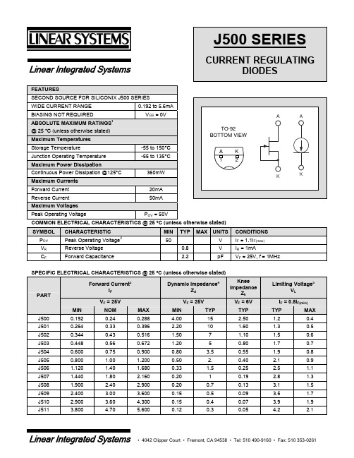
IF Zk VL VR IF
rDS VR
POV VF
IR
PACKAGING DETAILS
TБайду номын сангаас-92
0.175 0.195 0.130 0.155 0.045 0.060 0.170 0.195
LS XXX YYWW
0.016 0.022 0.500 0.610
0.014 0.020
1
2
0.095 0.105
PART
Linear Integrated Systems
• 4042 Clipper Court • Fremont, CA 94538 • Tel: 510 490-9160 • Fax: 510 353-0261
元器件交易网
V-I CHARACTERISTICS CURRENT REGULTING DIODE
1
CURRENT REGULATING DIODES
0.192 to 5.6mA VGS = 0V
TO-92 BOTTOM VIEW A 1 K 2
K
K
A
A
SPECIFIC ELECTRICAL CHARACTERISTICS @ 25 °C (unless otherwise stated) Forward Current3 IF VF = 25V MIN J500 J501 J502 J503 J504 J505 J506 J507 J508 J509 J510 J511 0.192 0.264 0.344 0.448 0.600 0.800 1.120 1.440 1.900 2.400 2.900 3.800 NOM 0.24 0.33 0.43 0.56 0.75 1.00 1.40 1.80 2.40 3.00 3.60 4.70 MAX 0.288 0.396 0.516 0.672 0.900 1.200 1.680 2.160 2.900 3.600 4.300 5.600 MIN 4.00 2.20 1.50 1.20 0.80 0.50 0.33 0.20 0.20 0.15 0.15 0.12 Dynamic Impedance4 Zd VF = 25V TYP 15 10 7 5 3.5 2. 1.5 1 0.7 0.5 0.4 0.3 Knee Impedance Zk VF = 6V TYP 2.50 1.60 1.10 0.80 0.55 0.40 0.25 0.19 0.13 0.09 0.07 0.05 Limiting Voltage5 VL IF = 0.8IF(min) TYP 1.2 1.3 1.5 1.7 1.9 2.1 2.5 2.8 3.1 3.5 3.9 4.2 MAX 0.4 0.5 0.6 0.7 0.8 0.9 1.1 1.3 1.5 1.7 1.9 2.1
5082-0012资料

DescriptionThis PIN diode chip is silicon dioxide or nitride passi-vated. The 5082-0012 has a planar construction. The fabrication processes are optimized for long term reliability and tightly controlled for uniformity in electrical performance.OutlineMaximum RatingsJunction Operating and StorageTemperature Range .............................-65°C to +150°C Soldering Temperature ..........+425°C for 1 min. max.5082-0012PIN Diode Chip for Hybrid MIC Switches/AttenuatorsData SheetFeatures•Low Series Resistance: 1.0Ω TypicalApplicationsThis general purpose PIN diode is intended for low power switching applications such as duplexers,antenna switching matrices, digital phase shifters, time multiplex filters, TR switches, pulse and amplitude modulators, limiters, leveling circuits, and attenuators.Electrical Specifications at T A = 25°CTypical ParametersNearest Typical Chip Equivalent Minimum Maximum Typical Reverse Part Packaged Breakdown Junction Series Typical Recovery Number Part No.VoltageCapacitance Resistance Lifetime Time 5082-5082-V BR (V)C j (pF)R S (Ω)τ (ns)t rr (ns)001230011500.12 1.0400100 Test V R = V BR V R = 50 V I F = 100 mA I F = 50 mA I F = 20 mA ConditionsMeasure f = 1 MHzf = 100 MHzI R = 250 mAV R = 10 V I R ≤ 10 mA90% RecoveryDimensions in millimeters (1/1000 inch)Assembly and Handling Procedures forPIN Chips1. StorageDevices should be stored in a dry nitrogen purged dessicator or equivalent.2. CleaningIf required, surface contamination may be removed with electronic grade solvents. Typical solvents, such as freon (T.F. or T.M.C.), acetone, deionized water, and methanol, or their locally approved equivalents, can be used singularly or in combinations. Typical cleaning times per solvent are one to three minutes. DI water and methanol should be used (in that order) in the final cleans. Final drying can be accomplished by placing the cleaned dice on clean filter paper and drying with an infrared lamp for 5-10 minutes. Acids such as hydrofluoric (HF), nitric (HN O3) and hydrochloric (HCl) should not be used.The effects of cleaning methods/solutions should be verified on small samples prior to submitting the entire lot.Following cleaning, dice should be either used in assembly (typically within a few hours) or stored in clean containers in a reducing atmosphere or a vacu-um chamber.3. Die Attacha. EutecticAuSn preform with stage temperature of 310°C for one minute max. AuGe preform with stage temperature of 390°C for one minute max.b. EpoxyFor epoxy die-attach, conductive silver-filled or gold-filled epoxies are recommended. This method can be used for all Avago PIN chips.4. Wire BondingEither ultrasonic or thermocompression bonding tech-niques can be employed. Suggested wire is pure gold, 0.7 to 1.5 mil diameter.For product information and a complete list of distributors, please go to our web site: Avago, Avago Technologies, and the A logo are trademarks of Avago Technologies, Pte. in the United States and other countries.Data subject to change. Copyright © 2006 Avago Technologies Pte. All rights reserved. Obsoletes 5965-8880E5989-4778EN February 23, 2006。
5082-5703-HK000中文资料

14.2 mm (0.56 inch)Seven Segment Displays Technical DataFeatures• Industry Standard Size • Industry Standard Pinout 15.24 mm (0.6 in.) DIP Leads on 2.54 mm (0.1 in.) Centers • Choice of ColorsAlGaAs Red, High Efficiency Red, Yellow, Green, Orange • Excellent Appearance Evenly Lighted Segments Mitered Corners on Segments Gray Package Gives Optimum Contrast±50° Viewing Angle • Design FlexibilityCommon Anode or Common CathodeSingle and Dual Digits Right Hand Decimal Point ±1. Overflow Character• Categorized for Luminous IntensityYellow and Green Categorized for ColorUse of Like Categories Yields a Uniform Display • High Light Output • High Peak Current• Excellent for Long Digit String Multiplexing • Intensity and Color Selection OptionSee Intensity and ColorSelected Displays Data Sheet • Sunlight Viewable AlGaAsDescriptionThe 14.2 mm (0.56 inch) LED seven segment displays aredesigned for viewing distances upto 7 metres (23 feet). Thesedevices use an industry standard size package and pinout. Both the numeric and ±1 overflow devices feature a right hand decimalpoint. All devices are available as either common anode or common cathode.Orange AlGaAs Red HERYellowGreen Package HDSP-HDSP-[1]HDSP-[1]HDSP-HDSP- DescriptionDrawingH401H151550157015601Common Anode Right Hand Decimal A H403H153550357035603Common Cathode Right Hand Decimal B H157550757075607Common Anode ±1. Overflow C H158550857085608Common Cathode ±1. OverflowD K401552157215621Two Digit Common Anode Right Hand DecimalE K403552357235623Two Digit Common Cathode Right Hand DecimalFDevicesNote:1. These displays are recommended for high ambient light operation. Please refer to the HDSP-H10X/K12X AlGaAs and HDSP-555X HER data sheet for low current operation.HDSP-K40x Series HDSP-550x Series HDSP-552x Series HDSP-560x Series HDSP-562x Series HDSP-570x Series HDSP-572x Series HDSP-H15x Series HDSP-H40x SeriesThese displays are ideal for most applications. Pin for pin equivalent displays are alsoavailable in a low current design.The low current displays are idealfor portable applications. For additional information see the Low Current Seven Segment Displays data sheet.Part Numbering SystemNotes:1. For codes not listed in the figure above, please refer to the respective datasheet or contact your nearest Agilent representative for details.2. Bin options refer to shippable bins for a part number. Color and Intensity Bins are typically restricted to 1bin per tube (exceptions may apply). Please refer to respective datasheet for specific bin limit information.5082 -X X X X-X X X X X HDSP-X X X X-X X X X XMechanical Options [1]00: No Mechanical Option Color Bin Options [1,2]0: No Color Bin LimitationMaximum Intensity Bin [1,2]0: No Maximum Intensity Bin Limitation Minimum Intensity Bin [1,2]0: No Minimum Intensity Bin Limitation Device Configuration/Color [1]1: Common Anode 3: Common CathodeDevice Specific Configuration [1]Refer to Respective DatasheetPackage [1]H: 14.2 mm (0.56 inch) Single Digit Seven Segment DisplayFUNCTIONPIN AB CDEF1CATHODE e ANODE e CATHODE c ANODE cE CATHODE NO. 1 E ANODE NO. 12CATHODE d ANODE d ANODE c, d CATHODE c, d D CATHODE NO. 1 D ANODE NO. 13ANODE [3]CATHODE [4]CATHODE b ANODE bC CATHODE NO. 1 C ANODE NO. 14CATHODE c ANODE c ANODE a, b, DP CATHODE a, b, DP DP CATHODE NO. 1DP ANODE NO. 15CATHODE DP ANODE DP CATHOPDE DP ANODE DE E CATHODE NO. 1 E ANODE NO. 26CATHODE b ANODE b CATHODE a ANODE aD CATHODE NO. 2 D ANODE NO. 27CATHODE a ANODE a ANODE a, b, DP CATHODE a, b, DP G CATHODE NO. 2G ANODE NO. 28ANODE [3]CATHODE [4]ANODE c, d CATHODE c, d C CATHODE NO. 2 C ANODE NO. 29CATHODE f ANODE f CATHODE d ANODE d DP CATHODE NO. 2DP ANODE NO. 210CATHODE g ANODE g NO PINNO PINB CATHODE NO. 2 B ANODE NO. 211 A CATHODE NO. 2 A ANODE NO. 212 F CATHODE NO. 2 F ANODE NO. 213DIGIT NO. 2 ANODE DIGIT NO. 2 CATHODE 14DIGIT NO. 1 ANODE DIGIT NO. 1 CATHODE 15 B CATHODE NO. 1 B ANODE NO. 116 A CATHODE NO. 1 A ANODE NO. 117G CATHODE NO. 1G ANODE NO. 118F CATHODE NO. 1 F ANODE NO. 1NOTES:1. ALL DIMENSIONS IN MILLIMETRES (INCHES).2. ALL UNTOLERANCED DIMENSIONS ARE FOR REFERENCE ONLY.3. REDUNDANT ANODES.4. REDUNDANT CATHODES.5. FOR HDSP-5600/-5700 SERIES PRODUCT ONLY.Package DimensionsInternal Circuit DiagramNotes:1. See Figure 2 to establish pulsed conditions.2. Derate above 46°C at 0.54 mA/°C.3. See Figure 7 to establish pulsed conditions.4. Derate above 53°C at 0.45 mA/°C.5. See Figure 8 to establish pulsed conditions.HER/Orange HDSP-5500AlGaAs Red HDSP-H40x Yellow Green HDSP-H150HDSP-K40x HDSP-5700HDSP-5600 Description SeriesSeriesSeriesSeriesUnits Average Power per Segment or DP 9610580105mW Peak Forward Current per 160[1]90[3]60[5]90[7]mA Segment or DPDC Forward Current per Segment or DP 40[2]30[4]20[6]3018]mA Operating Temperature Range -20 to +100[9]-40 to +100°C Storage Temperature Range -55 to +100°C Reverse Voltage per Segment or DP 3.0V Lead Solder Temperature for 3 Seconds 260°C(1.60 mm [0.063 in.] below seating plane)Absolute Maximum Ratings6. Derate above 81°C at 0.52 mA/°C.7. See Figure 9 to establish pulsed conditions.8. Derate above 39°C at 0.37 mA/°C.9. For operation below -20°C, contact your local Agilent components sales office or an authorized distributor.Electrical/Optical Characteristics at T A = 25°CAlGaAs RedDeviceSeriesHDSP- Parameter Symbol Min.Typ.Max.Units Test Conditions Luminous Intensity/Segment[1,2,5]I V9.116.0mcd I F = 20 mA(Digit Average)1.8I F = 20 mAForward Voltage/Segment or DP V F V2.03.0I F = 100 mAH15XPeak WavelengthλPEAK645nmDominant Wavelength[3]λd637nmReverse Voltage/Segment or DP[4]V R 3.015V I R = 100 µATemperature Coefficient of∆V F/°C-2mV/°CV F/Segment or DPThermal Resistance LED Junction-RθJ-Pin400°C/W/to-Pin SegHigh Efficiency RedDeviceSeriesHDSP- Parameter Symbol Min.Typ.Max.Units Test Conditions9002800I F = 10 mA Luminous Intensity/Segment[1,2,6]I Vµcd(Digit Average)3700I F = 60 mA Peak:1 of 6 dfForward Voltage/Segment or DP V F 2.1 2.5V I F = 20 mA 55XXPeak WavelengthλPEAK635nmDominant Wavelength[3]λd626nmReverse Voltage/Segment or DP[4]V R 3.030V I R = 100 µATemperature Coefficient of∆V F/°C-2mV/°CV F/Segment or DPThermal Resistance LED Junction-RθJ-Pin345°C/W/to-Pin SegYellowDeviceSeriesHDSP- Parameter Symbol Min.Typ.Max.Units Test Conditions6001800I F = 10 mA Luminous Intensity/Segment[1,2]I Vµcd(Digit Average)2750I F = 60 mA Peak:1 of 6 dfForward Voltage/Segment or DP V F 2.1 2.5V I F = 20 mA 57XXPeak WavelengthλPEAK583nmDominant Wavelength[3,7]λd581.5586592.5nmReverse Voltage/Segment or DP[4]V R 3.040V I R = 100 µATemperature Coefficient of∆V F/°C-2mV/°CV F/Segment or DPThermal Resistance LED Junction-RθJ-Pin345°C/W/to-Pin SegOrangeDeviceSeriesHDSP- Parameter Symbol Min.Typ.Max.Units Test Conditions Luminous Intensity/Segment I V 2.37mcd I F = 10 mA(Segment Average)[1,2]Forward Voltage/Segment or DP V F 2.1 2.5V I F = 20 mAPeak WavelengthλPEAK600nm H40x Dominant Wavelength[3]λd603nm I F = 10 mA K40x Reverse Voltage/Segment or DP[4]V R 3.030V I R = 100 µA Temperature Coefficient of∆V F/°C-2mV/°CV F/Segment or DPThermal Resistance LED Junction-RθJ-Pin345°C/W/to-Pin SegDeviceSeriesHDSP-ParameterSymbol Min.Typ.Max.UnitsTest Conditions 9002500I F = 10 mALuminous Intensity/Segment [1,2]I Vµcd(Digit Average)`3100I F = 60 mA Peak:1 of 6 df Forward Voltage/Segment or DPV F 2.1 2.5V I F = 10 mA56XXPeak Wavelength λPEAK 566nm Dominant Wavelength [3,7]λd 571577nm Reverse Voltage/Segment or DP [4]V R 3.050V I R = 100 µATemperature Coefficient of ∆V F /°C -2mV/°C V F /Segment or DPThermal Resistance LED Junction-R θJ-Pin345°C/W/to-PinSegHigh Performance GreenNotes:1. Device case temperature is 25°C prior to the intensity measurement.2. The digits are categorized for luminous intensity. The intensity category is designated by a letter on the side of the package.3. The dominant wavelength, λd , is derived from the CIE chromaticity diagram and is that single wavelength which defines the color of the device.4. Typical specification for reference only. Do not exceed absolute maximum ratings.5. For low current operation, the AlGaAs HDSP-H10X series displays are recommended. They are tested at 1 mA dc/segment and are pin for pin compatible with the HDSP-H15X series.6. For low current operation, the HER HDSP-555X series displays are recommended. They are tested at 2 mA dc/segment and are pin for pin compatible with the HDSP-550X series.7. The Yellow (HDSP-5700) and Green (HDSP-5600) displays are categorized for dominant wavelength. The category is designated by a number adjacent to the luminous intensity category letter.AlGaAs RedFigure 3. Maximum Allowable DC Current vs.Ambient Temperature.Figure 4. Forward Current vs.Forward Voltage.HER, Yellow, Green, OrangeFigure 7. Maximum Tolerable Peak Currentvs. Pulse Duration – HER, Orange.I D C M A X . – M A X I M U M D C C U R R E N T P E R S E G M E N T – m AT A – AMBIENT TEMPERATURE – °C 5030102051525354045I F – F O R W A R D C U R R E N T P E R S E G M E N T – m AV F – FORWARD VOLTAGE – VR E L A T I V E L U M I N O U S I N T E N S I T Y (N O R M A L I Z E D T O 1 A T 20 m A)I F – FORWARD CURRENT PER SEGMENT – mA204010305152535ηP E A K – N O R M A L IZ E D R E L A T I V E E F F I C I E N C YI PEAK – PEAK FORWARD CURRENTPER SEGMENT – mA4550110120Figure 11. Forward Current vs.Forward Voltage.Figure 9. Maximum Tolerable PeakCurrent vs. Pulse Duration – Green.Figure 10. Maximum Allowable DC Current vs.Ambient Temperature.Figure 12. Relative LuminousIntensity vs. DC Forward Current.Figure 13. Relative Efficiency (Luminous Intensity per Unit Current) vs. Peak Current.Electrical/OpticalFor more information onelectrical/optical characteristics,please see Application Note 1005.Contrast EnhancementFor information on contrastenhancement please see Application Note 1015.Soldering/CleaningCleaning agents from the ketone family (acetone, methyl ethyl ketone, etc.) and from thechlorinated hydrocarbon family(methylene chloride, trichloro–ethylene, carbon tetrachloride,etc.) are not recommended for cleaning LED parts. All of these various solvents attack or dissolve the encapsulating epoxies used to form the package of plastic LED parts.For information on soldering LEDs please refer to Application Note 1027.I F – F O R W A R D C U R R E N T P E R S E G M E N T – m AV F – FORWARD VOLTAGE – VR E L A T I V E L U M I N O U S I N T E N S I T Y (N O R M A L I Z E D A T 10 m A )I F – DC FORWARD CURRENT – mAηV – R E L A T I V E E F F I C I E N C Y (N O R M A L I Z E D T O 1 A T 10 m A P E R S E G ME N T )0.6I PEAK – PEAK FORWARD CURRENTPER SEGMENT – mA902070801001.61.41.31.10.90.860504030100.71.01.21.5HDSP-H15x IV Bin Category Min.Max.K 9.2016.90L 13.8025.30M 20.7038.00N 31.1056.90O 46.6085.40Intensity Bin Limits (mcd)AlGaAs RedHDSP-550x/552x IV Bin Category Min.Max.E 0.91 1.67F 1.37 2.51G 2.05 3.76H 3.08 5.64I 4.628.64J 6.9312.70K 10.3919.04HERHDSP-570x/572xIV Bin Category Min.Max.D 0.61 1.11E 0.91 1.67F 1.37 2.51G 2.05 3.76H 3.08 5.64I 4.628.64J 6.9312.70K 10.3919.04YellowHDSP-560x/562x IV Bin Category Min.Max.E 0.91 1.67F 1.37 2.51G 2.05 3.76H 3.08 5.64I 4.618.46GreenColor CategoriesNote:All categories are established for classification of products. Products may not be available in all categories. Please contact your Agilent representatives for further clarification/information.10HDSP-H40x/K40x IV Bin Category Min.Max.B 0.77 1.17C 0.95 1.45D 1.19 1.82E 1.49 2.27F 1.85 2.89G 2.32 3.54H 2.904.43Orange元器件交易网元器件交易网/semiconductorsFor product information and a complete list ofdistributors, please go to our web site.For technical assistance call:Americas/Canada: +1 (800) 235-0312 or(408) 654-8675Europe: +49 (0) 6441 92460China: 10800 650 0017Hong Kong: (+65) 271 2451India, Australia, New Zealand: (+65) 271 2394Japan: (+81 3) 3335-8152(Domestic/Interna-tional), or 0120-61-1280(Domestic Only)Korea: (+65) 271 2194Malaysia, Singapore: (+65) 271 2054Taiwan: (+65) 271 2654Data subject to change.Copyright © 2002 Agilent Technologies, Inc.Obsoletes 5988-0383ENJanuary 17, 20025988-4273EN。
危险化学品特性表_第3.3类

目录表—煤油的理化性质及危险特性1表—2,2-二甲基庚烷的理化性质及危险特性2表-3,4—二甲基庚烷的理化性质及危险特性3 表—正癸烷的理化性质及危险特性4表—硝基乙烷的理化性质及危险特性5表—1—溴丙烷的理化性质及危险特性6表—邻二甲苯的理化性质及危险特性6表- 间二甲苯的理化性质及危险特性7表-对二甲苯的理化性质及危险特性8表—二甲苯异构体混合物的理化性质及危险特性10 表-1,3,5—三甲基苯的理化性质及危险特性11 表—1,2,3-三甲基苯的理化性质及危险特性12 表-1,2,4-三甲基苯的理化性质及危险特性13 表—邻二乙基苯的理化性质及危险特性14表—甲基异丙基苯的理化性质及危险特性15 表—苯乙烯的理化性质及危险特性16表—正丁醇的理化性质及危险特性17表- 异丁醇的理化性质及危险特性18表-仲丁醇的理化性质及危险特性19表- 乙二醇甲醚的理化性质及危险特性20表- 乙二醇乙醚的理化性质及危险特性21表- 乙二醇二乙醚的理化性质及危险特性22表—乙二醇异丙醚的理化性质及危险特性23表—丙二醇乙醚的理化性质及危险特性24表—乙酸乙二醇乙醚的理化性质及危险特性25表- 正庚醛的理化性质及危险特性26表—二异丁基(甲)酮的理化性质及危险特性27表- 环己酮的理化性质及危险特性28表—原甲酸(三)乙酯的理化性质及危险特性29表—乙酸异戊酯的理化性质及危险特性30表- 丙酸正丁酯的理化性质及危险特性31表- 丙酸正戊酯的理化性质及危险特性32表- 丙烯酸正丁酯的理化性质及危险特性33表—甲基丙烯酸正丁酯[抑制了]的的理化性质及危险特性34 表- 甲基丙烯酸异丁酯的理化性质及危险特性35表—丙烯酸异丁酯[抑制了的]的理化性质及危险特性36 表—丙烯酸异辛酯的理化性质及危险特性37表- 乳酸甲酯的理化性质及危险特性38表—乳酸乙酯的理化性质及危险特性39表- 正硅酸乙酯的理化性质及危险特性40表—N,N—二甲基甲酰胺的理化性质和危险特性41表—乙烯三乙氧基硅烷的理化性质及危险特性42表- 松节油的理化性质及危险特性43表—松香水的理化性质和危险特性44表- 不饱和聚酯树脂的理化性质及危险特性45 表- 丁醇改性酚醛树脂的理化性质及危险特性46 表—聚氨酯树脂的理化性质及危险特性47 表—氨基树脂的理化性质及危险特性48表—不干性醇酸树脂的理化性质及危险特性50 表- 丙烯酸树脂的理化性质及危险特性51表- 丙烯酸底漆的理化性质及危险特性52 表—丙烯酸烘漆的理化性质及危险特性53表- 硝基腻子的理化性质及危险特性54表- 铝银浆的理化性质及危险特性55表- 醇酸清漆的理化性质及危险特性56表- 氨基清烘漆的理化性质及危险特性57表- 醇酸绝缘漆的理化性质及危险特性58 表—酚醛烘漆的理化性质及危险特性59表—酚醛清漆的理化性质及危险特性60表—银灰酚醛磁漆的理化性质及危险特性61 表—木材防腐漆的理化性质及危险特性62 表—柴油的理化性质及危险特性63表—一氯化苯的理化性质及危险特性64表—溴苯的理化性质及危险特性65表—糠醛的理化性质及危险特性66表- 吗啉的理化性质及危险特性67表- N,N-二甲基乙醇胺的理化性质及危险特性68 表—环戊醇的理化性质及危险特性69表—樟脑油的理化性质及危险特性70表—松油的理化性质及危险特性71表—戊烯的理化性质及危险特性72表—α-蒎烯的理化性质及危险特性73表-β-蒎烯的理化性质及危险特性74表—氨基透明烘漆的理化性质及危险特性75表-煤油的理化性质及危险特性表—正癸烷的理化性质及危险特性表—邻二甲苯的理化性质及危险特性表—间二甲苯的理化性质及危险特性表—对二甲苯的理化性质及危险特性表-二甲苯异构体混合物的理化性质及危险特性表-邻二乙基苯的理化性质及危险特性表—甲基异丙基苯的理化性质及危险特性表—苯乙烯的理化性质及危险特性表—丙二醇乙醚的理化性质及危险特性表—乙酸乙二醇乙醚的理化性质及危险特性表-正庚醛的理化性质及危险特性表-二异丁基(甲)酮的理化性质及危险特性表-环己酮的理化性质及危险特性表-原甲酸(三)乙酯的理化性质及危险特性表—乙酸异戊酯的理化性质及危险特性表-丙酸正丁酯的理化性质及危险特性表—丙酸正戊酯的理化性质及危险特性表—丙烯酸正丁酯的理化性质及危险特性表-甲基丙烯酸正丁酯[抑制了]的的理化性质及危险特性表—甲基丙烯酸异丁酯的理化性质及危险特性表—丙烯酸异丁酯[抑制了的]的理化性质及危险特性表-丙烯酸异辛酯的理化性质及危险特性表—乳酸甲酯的理化性质及危险特性表—乳酸乙酯的理化性质及危险特性表—正硅酸乙酯的理化性质及危险特性表—N,N—二甲基甲酰胺的理化性质和危险特性表-乙烯三乙氧基硅烷的理化性质及危险特性表-松节油的理化性质及危险特性表—松香水的理化性质和危险特性表-不饱和聚酯树脂的理化性质及危险特性表-丁醇改性酚醛树脂的理化性质及危险特性。
QRD330002资料
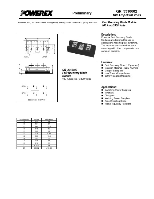
Powerex, Inc., 200 Hillis Street, Youngwood, Pennsylvania 15697-1800 (724) 925-7272Fast Recovery Diode Module 100 Amp/3300 VoltsDescription:Powerex Fast Recovery Diode Modules are designed for use inapplications requiring fast switching. The modules are isolated for easy mounting with other components on a common heatsink.Features:Fast Recovery Time (1.2 µs max.) Isolation Material – DBC Alumina Copper Baseplate Low Thermal Impedance 6000 V Isolated MountingApplications:Switching Power Supplies Inverters ChoppersWelding Power Supplies Free Wheeling DiodeHigh Frequency RectifiersQR_3310002Fast Recovery Diode Module100 Amperes / 3300 VoltsDimensions Inches MillimetersA 3.70 94B 1.34 34C 1.40 35.6D 3.15 80E 0.67 17F 0.28 6.99G 0.67 17.1H 0.91 23 J 0.36 9.0 K 1.18 30 L 0.216 5.5 M #10-32 #10-32Powerex, Inc., 200 Hillis Street, Youngwood, Pennsylvania 15697-1800 (724) 925-7272Fast Recovery Diode Module100 Amp/3300 VoltsAbsolute Maximum Ratings, T J =25°C unless otherwise specifiedCharacteristics Conditions Symbol QRD330002QRC330002 UnitsRepetitive Peak Reverse Blocking Voltage - V RRM 3300 Volts Non-Repetitive Peak Reverse Blocking Voltage - V RSMV RRM + 100VoltsAverage Forward Current Tc=25°C I F(AV) 100 AmperesForward CurrentPulse I FM 200 Amperes Operating Junction Temperature - T J -40 to 150 °C Storage Temperature- T STG -40 to 150 °C Maximum Mounting Torque, #10-32 Mounting Screw - - 26 In.-lb. Maximum Terminal Torque, #10-32 Terminal Screw - - 26 In.-lb. Module Weight (Typical) --250GramsV Isolation60 Hz, circuit to base, all terminalsshorted, t = 1 secV RMS 6000 VoltsElectrical Characteristics, T J =25°C unless otherwise specifiedCharacteristics Symbol Test Conditions Min. Typ. Max UnitsPeak Reverse Leakage Current I RRM Rated V RRM - - 5 mAPeak On-State Voltage V FM I F =100A - 3.3 4.3 VoltsReverse Recovery Time trr I F = 100A, di/dt = −200A/µs - - 1.2 µs Reverse Recovery Charge QrrI F =100A, di/dt = −200A/µs - 25 - µCThermal Characteristics, T J =25°C unless otherwise specifiedCharacteristics Symbol Min. Typ. Max. UnitsThermal Resistance, Junction to Case R ΘJC Per Diode - 0.115 TBD °C/Watt Thermal Resistance, Case to Sink LubricatedR ΘCS Per Module - - 0.05 °C/Watt。
美国安全数据表 CoolTherm UR-2000硬化剂产品说明说明书
USA SAFETY DATA SHEET3000010118511. CHEMICAL PRODUCT AND COMPANY IDENTIFICATIONProduct name: CoolTherm UR-2000 HARDENER Product Use/Class:Thermal Interface Mtl. Part BLORD Corporation 111 LORD DriveCary, NC 27511-7923 USATelephone: 814 868-3180Non-Transportation Emergency: 814 763-2345 Chemtrec 24 Hr Transportation Emergency No.800 424-9300 (Outside Continental U.S. 703 527-3887)EFFECTIVE DATE: 05/05/20202. HAZARDS IDENTIFICATIONGHS CLASSIFICATION:Acute toxicity Inhalation - Dust and MistCategory 4 Acute toxicity Inhalation - Vapours Category 4 Skin sensitization Category 1Respiratory sensitization Category 1 Reproductive toxicity Category 2Specific target organ systemic toxicity (single exposure) Category 1 Central nervous system, Respiratory system Specific target organ systemic toxicity (repeated exposure) Category 1 Respiratory system Hazardous to the aquatic environment - acute hazard Category 2 Hazardous to the aquatic environment - chronic hazard Category 2GHS LABEL ELEMENTS: Symbol(s)Signal WordD ANGERHazard StatementsHarmful if inhaled.May cause an allergic skin reaction.May cause allergy or asthma symptoms or breathing difficulties if inhaled. Suspected of damaging fertility or the unborn child.Causes damage to organs.(Central nervous system, Respiratory system)Causes damage to organs through prolonged or repeated exposure.(Respiratory system) Toxic to aquatic life.Toxic to aquatic life with long lasting effects.Precautionary Statements PreventionObtain special instructions before use.Do not handle until all safety precautions have been read and understood. Wear protective gloves.Use personal protective equipment as required.In case of inadequate ventilation wear respiratory protection. Do not breathe dust/fume/gas/mist/vapors/spray. Wash thoroughly after handling.Do not eat, drink or smoke when using this product.Use only outdoors or in a well-ventilated area.Contaminated work clothing should not be allowed out of the workplace.Avoid release to the environment.ResponseCall a POISON CENTER or doctor/physician if you feel unwell.IF exposed: Call a POISON CENTER or doctor/physician.Specific treatment (see supplemental first aid instructions on this label).IF INHALED: Remove to fresh air and keep at rest in a position comfortable for breathing.If experiencing respiratory symptoms: Call a POISON CENTER or doctor/physician.IF ON SKIN: Wash with plenty of soap and water.If skin irritation or rash occurs: Get medical advice/attention.Wash contaminated clothing before reuse.Collect spillage.StorageStore locked up.Disposal:Dispose of contents/container in accordance with waste/disposal laws and regulations of your country or particular locality.Other Hazards:This product contains component(s) which have the following warnings; however based on the GHS classification criteria of your country or locale, the product mixture may be outside the respective category(s).Acute: May be harmful if absorbed through skin. May cause lung damage. Possible irritation of the respiratorysystem can occur causing a variety of symptoms such as dryness of the throat, tightness of the chest, and shortness of breath. May be harmful if swallowed. Ingestion is not an expected route of entry in industrial or commercial uses.Chronic: May cause long-term lung damage. IARC has designated carbon black as Group 2B - inadequate evidence for carcinogenicity in humans, but sufficient evidence in experimental animals. In 2006 IARC reaffirmed its 1995 finding that there is "inadequate evidence" from human health studies to assess whether carbon black causes cancer in humans. Further, epidemiological evidence from well-conducted investigations has shown no causative link between carbon black exposure and the risk of malignant or non-malignant respiratory disease in humans.3. COMPOSITION/INFORMATION ON INGREDIENTSChemical Name CAS Number RangeAliphatic polyisocyanate PROPRIETARY10 - 15%Titanium dioxide13463-67-7 5 - 10%Phosphate compound PROPRIETARY 1 - 5%Methylene bis (4-cyclohexylisocyanate)5124-30-1 1 - 5%Any "PROPRIETARY" component(s) in the above table is considered trade secret, thus the specific chemical and its exact concentration is being withheld.4. FIRST AID MEASURESFIRST AID - EYE CONTACT: Flush eyes immediately with large amount of water for at least 15 minutes holding eyelids open while flushing. Get prompt medical attention.FIRST AID - SKIN CONTACT: Flush contaminated skin with large amounts of water while removing contaminated clothing. Wash affected skin areas with soap and water. Get medical attention if symptoms occur.FIRST AID - INHALATION: Move person to fresh air. Restore and support continued breathing. If breathing is difficult, give oxygen. Get immediate medical attention.FIRST AID - INGESTION: If swallowed, do not induce vomiting. Call a physician or poison control center immediately for further instructions. Never give anything by mouth if victim is rapidly losing consciousness, unconscious or convulsing.5. FIRE-FIGHTING MEASURESSUITABLE EXTINGUISHING MEDIA: Carbon Dioxide, Dry Chemical, Foam, Water FogUNSUITABLE EXTINGUISHING MEDIA: Not determined for this product.SPECIFIC HAZARDS POSSIBLY ARISING FROM THE CHEMICAL: Keep containers tightly closed. Closed containers may rupture when exposed to extreme heat. Use water spray to keep fire exposed containers cool. During a fire, irritating and/or toxic gases and particulate may be generated by thermal decomposition or combustion.SPECIAL PROTECTIVE EQUIPMENT AND PRECAUTIONS FOR FIRE-FIGHTERS: Wear full firefighting protective clothing, including self-contained breathing apparatus (SCBA). If water is used, fog nozzles are preferable.6. ACCIDENTAL RELEASE MEASURESPERSONAL PRECAUTIONS, PROTECTIVE EQUIPMENT AND EMERGENCY PROCEDURES: Avoid breathing vapors. Use self-contained breathing equipment. Avoid contact.ENVIRONMENTAL PRECAUTIONS: Do not contaminate bodies of water, waterways, or ditches, with chemical or used container.METHODS AND MATERIALS FOR CONTAINMENT AND CLEANUP: Keep non-essential personnel a safe distance away from the spill area. Notify appropriate authorities if necessary. Avoid contact. Before attempting cleanup, refer to hazard caution information in other sections of the SDS form. Scoop spilled material into an appropriate container for proper disposal. (If necessary, use inert absorbent material to aid in containing the spill).7. HANDLING AND STORAGEHANDLING: Keep closure tight and container upright to prevent leakage. Avoid skin and eye contact. Wash thoroughly after handling. Avoid breathing of vapor or spray mists. Do not handle until all safety precautions have been read and understood. Empty containers should not be re-used. Use with adequate ventilation.STORAGE: Store only in well-ventilated areas. Keep container closed when not in use.INCOMPATIBILITY: Strong oxidizers, acids, bases, water.; This product will react with any materials containing active hydrogens, such as water, alcohol, ammonia, amines, alkalies and acids. The reaction with water is accelerated at temperatures higher than 122F (50C) and in the presence of alkalies, tertiary amines, and metal compounds. Some reactions can be violent.8. EXPOSURE CONTROLS/PERSONAL PROTECTIONCOMPONENT EXPOSURE LIMITChemical Name ACGIH TLV-TWA ACGIH TLV-STELOSHA PEL-TWAOSHA PEL-CEILINGSkinAliphatic polyisocyanate N.E.N.E.N.E. N.E.N.A.Titanium dioxide10 mg/m3N.E.15 mg/m3 N.E.N.A.Phosphate compound N.E.N.E.N.E. N.E.N.A.Methylene bis (4-cyclohexylisocyanate)0.005 ppm N.E.N.E. N.E.SN.A. - Not Applicable, N.E. - Not Established, S - Skin DesignationEngineering controls: Sufficient ventilation in pattern and volume should be provided in order to maintain air contaminant levels below recommended exposure limits.PERSONAL PROTECTION MEASURES/EQUIPMENT:RESPIRATORY PROTECTION: This product contains isocyanates which have poor odor warning properties. If occupational exposure limits are exceeded, a NIOSH approved supplied-air respirator is required. For respirator use observe OSHA regulations (29CFR 1910.134) or use in accordance with applicable laws and regulations of your country or particular locality.SKIN PROTECTION: Use neoprene, nitrile, or rubber gloves to prevent skin contact.EYE PROTECTION: Use safety eyewear including safety glasses with side shields and chemical goggles where splashing may occur.OTHER PROTECTIVE EQUIPMENT: Use disposable or impervious clothing if work clothing contamination is likely. Remove and wash contaminated clothing before reuse. Use long-sleeved shirt to minimize skin exposure.HYGIENIC PRACTICES: Wash hands before eating, smoking, or using toilet facility. Food or beverages should not be consumed anywhere this product is handled or stored. Wash thoroughly after handling.9. PHYSICAL AND CHEMICAL PROPERTIESTypical values, not to be used for specification purposes.ODOR: Sweet VAPOR PRESSURE: N.D.APPEARANCE: White to gray VAPOR DENSITY: Heavier than Air PHYSICAL STATE: Paste LOWER EXPLOSIVE LIMIT: Not ApplicableFLASH POINT:≥ 201 °F, 93 °CUPPER EXPLOSIVE LIMIT: Not ApplicableSetaflash Closed CupBOILING RANGE: N.A.EVAPORATION RATE: Slower than n-butyl-acetate AUTOIGNITION TEMPERATURE:N.D.DENSITY: 2.81 g/cm3 - 23.40 lb/gal DECOMPOSITION TEMPERATURE:N.D. VISCOSITY, DYNAMIC: ≥161,000 mPa.s @ 25 °C ODOR THRESHOLD: N.D.VISCOSITY, KINEMATIC: ≥57,295 mm2/s @ 25 °CSOLUBILITY IN H2O: Insoluble VOLATILE BY WEIGHT: 0.20 %pH: N.A.VOLATILE BY VOLUME: 0.57 %FREEZE POINT: N.D. VOC CALCULATED: 0.05 lb/gal, 5 g/l COEFFICIENT OF WATER/OILN.D.DISTRIBUTION:LEGEND: N.A. - Not Applicable, N.E. - Not Established, N.D. - Not Determined10. STABILITY AND REACTIVITYHAZARDOUS POLYMERIZATION: Hazardous polymerization will not occur under normal conditions.STABILITY: Product is stable under normal storage conditions.CONDITIONS TO AVOID: Moisture.; High temperatures.; Unwanted, rapid and potentially hazardous polymerization may occur upon reaction with water at high temperatures or in the presence of alkalies, tertiary amines, and metal compounds.INCOMPATIBILITY: Strong oxidizers, acids, bases, water.; This product will react with any materials containing active hydrogens, such as water, alcohol, ammonia, amines, alkalies and acids. The reaction with water is accelerated at temperatures higher than 122F (50C) and in the presence of alkalies, tertiary amines, and metal compounds. Some reactions can be violent.HAZARDOUS DECOMPOSITION PRODUCTS: Monomeric isocyanate, traces of hydrogen cyanide, nitrogen dioxide, Carbon monoxide, carbon dioxide, Metal oxides, Oxides of phosphorus11. TOXICOLOGICAL INFORMATIONEXPOSURE PATH: Refer to section 2 of this SDS.SYMPTOMS:Refer to section 2 of this SDS.TOXICITY MEASURES:Chemical Name LD50/LC50Aliphatic polyisocyanate GHS LC50 (vapour): Acute toxicity point estimate11 mg/l GHS LC50(dust and mist): Acute toxicity point estimate1.5 mg/lTitanium dioxide Oral LD50: Rat> 10,000 mg/kgDermal LD50: rabbit> 5,000 mg/kgGHS LC50 (vapour): Acute toxicity point estimate55 mg/l Phosphate compound Oral LD50: rat5,000 mg/kgOral LD50: Rat> 5 g/kgDermal LD50: rabbit> 2,000 mg/kgGHS LC50 (dust and mist): rat400 mg/m3/6 hMethylene bis (4-cyclohexylisocyanate) Oral LD50: Rat9,900 mg/kgDermal LD50: Rabbit> 10,000 mg/kg Inhalation LC50: Rat434 mg/m3/4 hGerm cell mutagenicity: No classification proposedCarcinogenicity: No classification proposedReproductive toxicity: Category 2 - Suspected of damaging fertility or the unborn child.Components contributing to classification: Methylene bis (4-cyclohexylisocyanate).12. ECOLOGICAL INFORMATION ECOTOXICITY:Chemical Name EcotoxicityAliphatic polyisocyanate Fish: Danio rerio (zebra fish)> 100 mg/l96 hTitanium dioxide N.D.Phosphate compound Invertebrates: Daphnia magna (Water flea)0.202 mg/l48 hPlants: Scenedesmus capricornutum (fresh water algae)3 mg/l96 hMethylene bis (4-cyclohexylisocyanate) Fish: Brachydanio rerio1.2 mg/l96 h Static Brachydanio rerio1.2 - 2.76 mg/l96 hPERSISTENCE AND DEGRADABILITY:Not determined for this product.BIOACCUMULATIVE: Not determined for this product.MOBILITY IN SOIL: Not determined for this product.OTHER ADVERSE EFFECTS: Not determined for this product.13. DISPOSAL CONSIDERATIONSDISPOSAL METHOD: Disposal should be done in accordance with Federal (40CFR Part 261), state and local environmental control regulations. If waste is determined to be hazardous, use licensed hazardous waste transporter and disposal facility.14. TRANSPORT INFORMATIONUS DOT RoadProper Shipping Name: Environmentally hazardous substances, solid, n.o.s.Hazard Class: 9SECONDARY HAZARD: NoneUN/NA Number: 3077Packing Group: IIIEmergency Response Guide Number: 171For US DOT non-bulk road shipments this material may be classified as NOT REGULATED. For the most accurate shipping information, refer to your transportation/compliance department regarding changes inpackage size, mode of shipment or other regulatory descriptors.IATA CargoPROPER SHIPPING NAME: Environmentally hazardous substance, solid, n.o.s.Hazard Class: 9HAZARD CLASS: NoneUN NUMBER: 3077PACKING GROUP: IIIEMS: 9LIMDGPROPER SHIPPING NAME: Environmentally hazardous substance, solid, n.o.s.Hazard Class: 9HAZARD CLASS: NoneUN NUMBER: 3077PACKING GROUP: IIIEMS: F-AThe listed transportation classification applies to non-bulk shipments. It does not address regulatory variations due to changes in package size, mode of shipment or other regulatory descriptors. For the most accurate shipping information, refer to your transportation/compliance department.15. REGULATORY INFORMATIONU.S. FEDERAL REGULATIONS: AS FOLLOWS:SARA SECTION 313This product contains the following substances subject to the reporting requirements of Section 313 of Title III of the Superfund Amendment and Reauthorization Act of 1986 and 40 CFR part 372.:Chemical Name CAS Number Weight % Less ThanMethylene bis (4-cyclohexylisocyanate)5124-30-1 5.0%TOXIC SUBSTANCES CONTROL ACT:INVENTORY STATUSThe chemical substances in this product are on the TSCA Section 8 Inventory.EXPORT NOTIFICATIONThis product contains the following chemical substances subject to the reporting requirements of TSCA 12(B) if exported from the United States:None16. OTHER INFORMATIONUnder HazCom 2012 it is optional to continue using the HMIS rating system. It is important to ensure employees have been trained to recognize the different numeric ratings associated with the HazCom 2012 and HMIS schemes.HMIS RATINGS - HEALTH: 2* FLAMMABILITY: 1 PHYSICAL HAZARD: 1* - Indicates a chronic hazard; see Section 2Revision: Section 9Effective Date: 05/05/2020DISCLAIMERThe information contained herein is, to the best of our knowledge and belief, accurate. However, since the conditions of handling and use are beyond our control, we make no guarantee of results, and assume no liability for damages incurred by use of this material. It is the responsibility of the user to comply with all applicable federal, state and local laws and regulations.。
- 1、下载文档前请自行甄别文档内容的完整性,平台不提供额外的编辑、内容补充、找答案等附加服务。
- 2、"仅部分预览"的文档,不可在线预览部分如存在完整性等问题,可反馈申请退款(可完整预览的文档不适用该条件!)。
- 3、如文档侵犯您的权益,请联系客服反馈,我们会尽快为您处理(人工客服工作时间:9:00-18:30)。
14.2 mm (0.56 inch)Seven Segment Displays Technical DataFeatures• Industry Standard Size • Industry Standard Pinout 15.24 mm (0.6 in.) DIP Leads on 2.54 mm (0.1 in.) Centers • Choice of ColorsAlGaAs Red, High Efficiency Red, Yellow, Green, Orange • Excellent Appearance Evenly Lighted Segments Mitered Corners on Segments Gray Package Gives Optimum Contrast±50° Viewing Angle • Design FlexibilityCommon Anode or Common CathodeSingle and Dual Digits Right Hand Decimal Point ±1. Overflow Character• Categorized for Luminous IntensityYellow and Green Categorized for ColorUse of Like Categories Yields a Uniform Display • High Light Output • High Peak Current• Excellent for Long Digit String Multiplexing • Intensity and Color Selection OptionSee Intensity and ColorSelected Displays Data Sheet • Sunlight Viewable AlGaAsDescriptionThe 14.2 mm (0.56 inch) LED seven segment displays aredesigned for viewing distances upto 7 metres (23 feet). Thesedevices use an industry standard size package and pinout. Both the numeric and ±1 overflow devices feature a right hand decimalpoint. All devices are available as either common anode or common cathode.Orange AlGaAs Red HERYellowGreen Package HDSP-HDSP-[1]HDSP-[1]HDSP-HDSP- DescriptionDrawingH401H151550157015601Common Anode Right Hand Decimal A H403H153550357035603Common Cathode Right Hand Decimal B H157550757075607Common Anode ±1. Overflow C H158550857085608Common Cathode ±1. OverflowD K401552157215621Two Digit Common Anode Right Hand DecimalE K403552357235623Two Digit Common Cathode Right Hand DecimalFDevicesNote:1. These displays are recommended for high ambient light operation. Please refer to the HDSP-H10X/K12X AlGaAs and HDSP-555X HER data sheet for low current operation.HDSP-K40x Series HDSP-550x Series HDSP-552x Series HDSP-560x Series HDSP-562x Series HDSP-570x Series HDSP-572x Series HDSP-H15x Series HDSP-H40x SeriesThese displays are ideal for most applications. Pin for pin equivalent displays are alsoavailable in a low current design.The low current displays are idealfor portable applications. For additional information see the Low Current Seven Segment Displays data sheet.Part Numbering SystemNotes:1. For codes not listed in the figure above, please refer to the respective datasheet or contact your nearest Agilent representative for details.2. Bin options refer to shippable bins for a part number. Color and Intensity Bins are typically restricted to 1bin per tube (exceptions may apply). Please refer to respective datasheet for specific bin limit information.5082 -X X X X-X X X X X HDSP-X X X X-X X X X XMechanical Options [1]00: No Mechanical Option Color Bin Options [1,2]0: No Color Bin LimitationMaximum Intensity Bin [1,2]0: No Maximum Intensity Bin Limitation Minimum Intensity Bin [1,2]0: No Minimum Intensity Bin Limitation Device Configuration/Color [1]1: Common Anode 3: Common CathodeDevice Specific Configuration [1]Refer to Respective DatasheetPackage [1]H: 14.2 mm (0.56 inch) Single Digit Seven Segment DisplayFUNCTIONPIN AB CDEF1CATHODE e ANODE e CATHODE c ANODE cE CATHODE NO. 1 E ANODE NO. 12CATHODE d ANODE d ANODE c, d CATHODE c, d D CATHODE NO. 1 D ANODE NO. 13ANODE [3]CATHODE [4]CATHODE b ANODE bC CATHODE NO. 1 C ANODE NO. 14CATHODE c ANODE c ANODE a, b, DP CATHODE a, b, DP DP CATHODE NO. 1DP ANODE NO. 15CATHODE DP ANODE DP CATHOPDE DP ANODE DE E CATHODE NO. 1 E ANODE NO. 26CATHODE b ANODE b CATHODE a ANODE aD CATHODE NO. 2 D ANODE NO. 27CATHODE a ANODE a ANODE a, b, DP CATHODE a, b, DP G CATHODE NO. 2G ANODE NO. 28ANODE [3]CATHODE [4]ANODE c, d CATHODE c, d C CATHODE NO. 2 C ANODE NO. 29CATHODE f ANODE f CATHODE d ANODE d DP CATHODE NO. 2DP ANODE NO. 210CATHODE g ANODE g NO PINNO PINB CATHODE NO. 2 B ANODE NO. 211 A CATHODE NO. 2 A ANODE NO. 212 F CATHODE NO. 2 F ANODE NO. 213DIGIT NO. 2 ANODE DIGIT NO. 2 CATHODE 14DIGIT NO. 1 ANODE DIGIT NO. 1 CATHODE 15 B CATHODE NO. 1 B ANODE NO. 116 A CATHODE NO. 1 A ANODE NO. 117G CATHODE NO. 1G ANODE NO. 118F CATHODE NO. 1 F ANODE NO. 1NOTES:1. ALL DIMENSIONS IN MILLIMETRES (INCHES).2. ALL UNTOLERANCED DIMENSIONS ARE FOR REFERENCE ONLY.3. REDUNDANT ANODES.4. REDUNDANT CATHODES.5. FOR HDSP-5600/-5700 SERIES PRODUCT ONLY.Package DimensionsInternal Circuit DiagramNotes:1. See Figure 2 to establish pulsed conditions.2. Derate above 46°C at 0.54 mA/°C.3. See Figure 7 to establish pulsed conditions.4. Derate above 53°C at 0.45 mA/°C.5. See Figure 8 to establish pulsed conditions.HER/Orange HDSP-5500AlGaAs Red HDSP-H40x Yellow Green HDSP-H150HDSP-K40x HDSP-5700HDSP-5600 Description SeriesSeriesSeriesSeriesUnits Average Power per Segment or DP 9610580105mW Peak Forward Current per 160[1]90[3]60[5]90[7]mA Segment or DPDC Forward Current per Segment or DP 40[2]30[4]20[6]3018]mA Operating Temperature Range -20 to +100[9]-40 to +100°C Storage Temperature Range -55 to +100°C Reverse Voltage per Segment or DP 3.0V Lead Solder Temperature for 3 Seconds 260°C(1.60 mm [0.063 in.] below seating plane)Absolute Maximum Ratings6. Derate above 81°C at 0.52 mA/°C.7. See Figure 9 to establish pulsed conditions.8. Derate above 39°C at 0.37 mA/°C.9. For operation below -20°C, contact your local Agilent components sales office or an authorized distributor.Electrical/Optical Characteristics at T A = 25°CAlGaAs RedDeviceSeriesHDSP- Parameter Symbol Min.Typ.Max.Units Test Conditions Luminous Intensity/Segment[1,2,5]I V9.116.0mcd I F = 20 mA(Digit Average)1.8I F = 20 mAForward Voltage/Segment or DP V F V2.03.0I F = 100 mAH15XPeak WavelengthλPEAK645nmDominant Wavelength[3]λd637nmReverse Voltage/Segment or DP[4]V R 3.015V I R = 100 µATemperature Coefficient of∆V F/°C-2mV/°CV F/Segment or DPThermal Resistance LED Junction-RθJ-Pin400°C/W/to-Pin SegHigh Efficiency RedDeviceSeriesHDSP- Parameter Symbol Min.Typ.Max.Units Test Conditions9002800I F = 10 mA Luminous Intensity/Segment[1,2,6]I Vµcd(Digit Average)3700I F = 60 mA Peak:1 of 6 dfForward Voltage/Segment or DP V F 2.1 2.5V I F = 20 mA 55XXPeak WavelengthλPEAK635nmDominant Wavelength[3]λd626nmReverse Voltage/Segment or DP[4]V R 3.030V I R = 100 µATemperature Coefficient of∆V F/°C-2mV/°CV F/Segment or DPThermal Resistance LED Junction-RθJ-Pin345°C/W/to-Pin SegYellowDeviceSeriesHDSP- Parameter Symbol Min.Typ.Max.Units Test Conditions6001800I F = 10 mA Luminous Intensity/Segment[1,2]I Vµcd(Digit Average)2750I F = 60 mA Peak:1 of 6 dfForward Voltage/Segment or DP V F 2.1 2.5V I F = 20 mA 57XXPeak WavelengthλPEAK583nmDominant Wavelength[3,7]λd581.5586592.5nmReverse Voltage/Segment or DP[4]V R 3.040V I R = 100 µATemperature Coefficient of∆V F/°C-2mV/°CV F/Segment or DPThermal Resistance LED Junction-RθJ-Pin345°C/W/to-Pin SegOrangeDeviceSeriesHDSP- Parameter Symbol Min.Typ.Max.Units Test Conditions Luminous Intensity/Segment I V 2.37mcd I F = 10 mA(Segment Average)[1,2]Forward Voltage/Segment or DP V F 2.1 2.5V I F = 20 mAPeak WavelengthλPEAK600nm H40x Dominant Wavelength[3]λd603nm I F = 10 mA K40x Reverse Voltage/Segment or DP[4]V R 3.030V I R = 100 µA Temperature Coefficient of∆V F/°C-2mV/°CV F/Segment or DPThermal Resistance LED Junction-RθJ-Pin345°C/W/to-Pin SegDeviceSeries HDSP-ParameterSymbol Min.Typ.Max.UnitsTest Conditions 9002500I F = 10 mALuminous Intensity/Segment [1,2]I Vµcd(Digit Average)`3100I F = 60 mA Peak:1 of 6 df Forward Voltage/Segment or DPV F 2.1 2.5V I F = 10 mA56XXPeak Wavelength λPEAK 566nm Dominant Wavelength [3,7]λd 571577nm Reverse Voltage/Segment or DP [4]V R 3.050V I R = 100 µATemperature Coefficient of ∆V F /°C -2mV/°C V F /Segment or DPThermal Resistance LED Junction-R θJ-Pin345°C/W/to-PinSegHigh Performance GreenNotes:1. Device case temperature is 25°C prior to the intensity measurement.2. The digits are categorized for luminous intensity. The intensity category is designated by a letter on the side of the package.3. The dominant wavelength, λd , is derived from the CIE chromaticity diagram and is that single wavelength which defines the color of the device.4. Typical specification for reference only. Do not exceed absolute maximum ratings.5. For low current operation, the AlGaAs HDSP-H10X series displays are recommended. They are tested at 1 mA dc/segment and are pin for pin compatible with the HDSP-H15X series.6. For low current operation, the HER HDSP-555X series displays are recommended. They are tested at 2 mA dc/segment and are pin for pin compatible with the HDSP-550X series.7. The Yellow (HDSP-5700) and Green (HDSP-5600) displays are categorized for dominant wavelength. The category is designated by a number adjacent to the luminous intensity category letter.AlGaAs RedFigure 2. Maximum Tolerable Peak Current vs. Pulse Duration – AlGaAs Red.Figure 1. Maximum Tolerable Peak Current vs.Pulse Duration – Red.Figure 3. Maximum Allowable DC Current vs.Ambient Temperature.Figure 4. Forward Current vs.Forward Voltage.HER, Yellow, Green, OrangeFigure 7. Maximum Tolerable Peak Currentvs. Pulse Duration – HER, Orange.Figure 8. Maximum Tolerable Peak Current vs. Pulse Duration – Yellow.Figure 5. Relative Luminous Intensity vs. DC Forward Current.Figure 6. Relative Efficiency (Luminous Intensity per Unit Current) vs. Peak Current.I D C M A X . – M A X I M U M D C C U R R E N T P E R S E G M E N T – m AT A – AMBIENT TEMPERATURE – °C 5030102051525354045I F – F O R W A R D C U R R E N T P E R S E G M E N T – m AV F – FORWARD VOLTAGE – VR E L A T I V E L U M I N O U S I N T E N S I T Y (N O R M A L I Z E D T O 1 A T 20 m A )I F – FORWARD CURRENT PER SEGMENT – mA204010305152535ηP E A K – N O R M A L IZ E D R E L A T I V E E F F I C I E N C YI PEAK – PEAK FORWARD CURRENTPER SEGMENT – mA40051015202530352010090807060504030T – AMBIENT TEMPERATURE – °C AI M A X – M A X I M U M D C C U R R E N T P E R S E G M E N T – m AD C 4550110120Figure 11. Forward Current vs.Forward Voltage.Figure 9. Maximum Tolerable PeakCurrent vs. Pulse Duration – Green.Figure 10. Maximum Allowable DC Current vs.Ambient Temperature.Figure 12. Relative LuminousIntensity vs. DC Forward Current.Figure 13. Relative Efficiency (Luminous Intensity per Unit Current) vs. Peak Current.Electrical/OpticalFor more information onelectrical/optical characteristics,please see Application Note 1005.Contrast EnhancementFor information on contrastenhancement please see Application Note 1015.Soldering/CleaningCleaning agents from the ketone family (acetone, methyl ethyl ketone, etc.) and from thechlorinated hydrocarbon family(methylene chloride, trichloro–ethylene, carbon tetrachloride,etc.) are not recommended for cleaning LED parts. All of these various solvents attack or dissolve the encapsulating epoxies used to form the package of plastic LED parts.For information on soldering LEDs please refer to Application Note 1027.I F – F O R W A R D C U R R E N T P E R S E G M E N T – m AV F – FORWARD VOLTAGE – VR E L A T I V E L U M I N O U S I N T E N S I T Y (N O R M A L I Z E D A T 10 m A )I F – DC FORWARD CURRENT – mAηV – R E L A T I V E E F F I C I E N C Y (N O R M A L I Z E D T O 1 A T 10 m A P E R S E G M EN T )0.6I PEAK – PEAK FORWARD CURRENTPER SEGMENT – mA902070801001.61.41.31.10.90.860504030100.71.01.21.5HDSP-H15x IV Bin Category Min.Max.K 9.2016.90L 13.8025.30M 20.7038.00N 31.1056.90O 46.6085.40Intensity Bin Limits (mcd)AlGaAs RedHDSP-550x/552x IV Bin Category Min.Max.E 0.91 1.67F 1.37 2.51G 2.05 3.76H 3.08 5.64I 4.628.64J 6.9312.70K 10.3919.04HERHDSP-570x/572xIV Bin Category Min.Max.D 0.61 1.11E 0.91 1.67F 1.37 2.51G 2.05 3.76H 3.08 5.64I 4.628.64J 6.9312.70K 10.3919.04YellowHDSP-560x/562x IV Bin Category Min.Max.E 0.91 1.67F 1.37 2.51G 2.05 3.76H 3.08 5.64I 4.618.46GreenColor CategoriesNote:All categories are established for classification of products. Products may not be available in all categories. Please contact your Agilent representatives for further clarification/information.10HDSP-H40x/K40x IV Bin Category Min.Max.B 0.77 1.17C 0.95 1.45D 1.19 1.82E 1.49 2.27F 1.85 2.89G 2.32 3.54H 2.904.43Orange元器件交易网元器件交易网/semiconductorsFor product information and a complete list ofdistributors, please go to our web site.For technical assistance call:Americas/Canada: +1 (800) 235-0312 or(408) 654-8675Europe: +49 (0) 6441 92460China: 10800 650 0017Hong Kong: (+65) 271 2451India, Australia, New Zealand: (+65) 271 2394Japan: (+81 3) 3335-8152(Domestic/Interna-tional), or 0120-61-1280(Domestic Only)Korea: (+65) 271 2194Malaysia, Singapore: (+65) 271 2054Taiwan: (+65) 271 2654Data subject to change.Copyright © 2002 Agilent Technologies, Inc.Obsoletes 5988-0383ENJanuary 17, 20025988-4273EN。