CT-1205中文资料
BT-120中文资料
©2008 Amp’ed RF Inc
1722 Ringwood Ave, Suite 250, San Jose, CA 95131, USA
BT-120/121 Datasheet Page 5 of 6
元器件交易网
Amp’ed RF, Inc.
元器件交易网
Amp’ed RF, Inc.
(phone) 408 213-9530 (fax) 408 213-9533
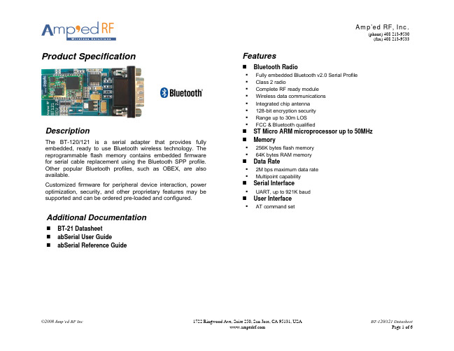
Product Specification
Features
Bluetooth Radio
Fully embedded Bluetooth v2.0 Serial Profile Class 2 radio Complete RF ready module Wireless data communications Integrated chip antenna 128-bit encryption security Range up to 30m LOS FCC & Bluetooth qualified
1722 Ringwood Ave, Suite 250, San Jose, CA 95131, USA
BT-120/121 Datasheet Page 4 of 6
元器件交易网
Amp’ed RF, Inc.
(phone) 408 213-9530 (fax) 408 213-9533
BT-120/121 Datasheet Page 2 of 6
元器件交易网
Amp’ed RF, Inc.
(phone) 408 213-9530 (fax) 408 213-9533
Serial Interface AT Commands
中日材料对照
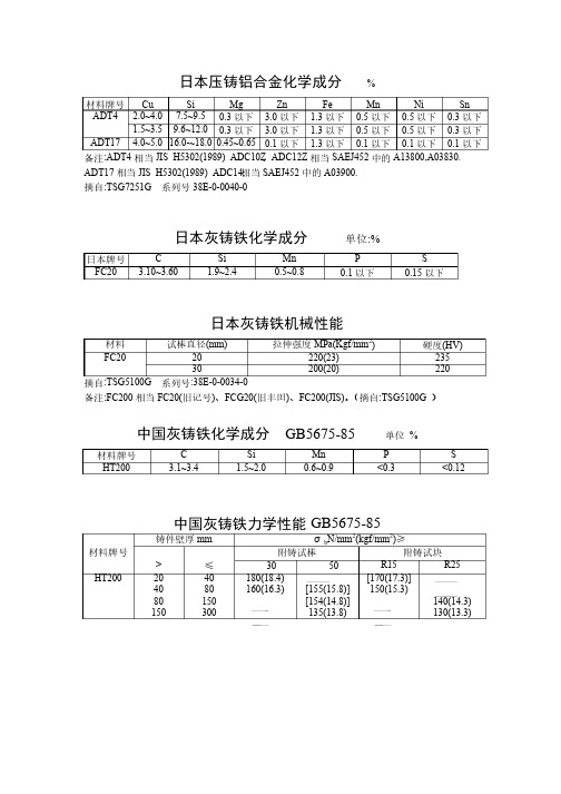
材料牌号材料牌号 Cu Si Mg Zn Fe Mn Ni Sn ADT4 2.0~4.0 7.5~9.5 0.3以下以下 3.0以下以下 1.3以下以下 0.5以下以下 0.5以下以下 0.3以下以下1.5~3.5 9.6~12.0 0.3以下以下3.0以下以下 1.3以下以下 0.5以下以下 0.5以下以下 0.3以下以下ADT17 4.0~5.0 16.0-~18.0 16.0-~18.0 0.45~0.65 0.45~0.65 0.1以下以下 1.3以下以下 0.1以下以下 0.1以下以下 0.1以下以下 日本牌号日本牌号C Si Mn P S FC20 3.10~3.60 1.9~2.4 0.5~0.8 0.1以下以下0.15以下以下材料材料 试棒直径(mm) 拉伸强度MPa(Kgf/mm 2) 硬度(HV) FC20 20 220(23) 235 30 200(20) 220 摘自:TSG5100G 系列号:38E-0-0034-0 材料牌号材料牌号C Si Mn P S HT200 3.1~3.4 1.5~2.0 0.6~0.9 <0.3 <0.12 中国灰铸铁力学性能GB5675-85 铸件壁厚mm σb N/mm 2(kgf/mm 2)≥材料牌号材料牌号附铸试棒附铸试棒 附铸试块附铸试块> ≤ 30 50 R15 R25 HT200 20 40 80 150 40 80 150 300 180(18.4) 160(16.3) [155(15.8)] [154(14.8)] 135(13.8) [170(17.3)] 150(15.3) 140(14.3) 130(13.3) 日本优质碳素结构钢机械性能表JISG4051 材料牌号材料牌号 热处理热处理 屈服点屈服点 不小于Kgf/mm 2 抗拉强度不小于Kgf/mm 2伸长率(%) 不小于不小于收缩率(%) 不小于不小于 冲击值冲击值 不小于Kgf*m/cm 2硬度硬度 HB 有效直径mm S10C 正火正火退火退火 21 32 33 109~146 109~149 S15C 正火正火 退火退火 24 38 30 111~167 111~149 S28C S30C 正火正火 退火退火 淬回火淬回火 29 34 48 55 25 23 57 11 137~197 126~156 152~212 30 S35C 正回火正回火 退火退火 淬回火淬回火 31 40 52 58 23 22 50 10 149~207 126~163 167~235 32 S38C S40C 正火正火 退火退火 淬回火淬回火 33 45 55 62 22 20 50 9 156~217 131~163 179~255 35 S43C S45C 正火正火 退火退火 淬回火淬回火 35 50 58 70 20 17 45 3 167~229 137~170 201~269 37 S48C S50C 正火正火 退火退火 淬回火淬回火 37 55 62 75 16 15 40 7 179~235 143~187 212~277 40 S53C S55C 正火正火 退火退火淬回火淬回火 40 60 66 80 15 14 35 6 183~255 149~192 299~285 42 摘自:《中外常用金属材料手册》陕西省标准化情报研究所编P362. 日本优质碳素结构钢化学成分表 单位%序号序号 材料牌号材料牌号 C Si Mn P 以下以下 S 以下以下 1 S10 0.08~0.13 0.15~0.35 0.3~0.6 0.03 0.035 2 S10C 0.08~0.13 0.15~0.35 0.3~0.6 0.03 0.035 3 S15 0.13~0.18 0.15~0.35 0.3~0.6 0.03 0.035 4 S25 0.22~0.28 0.15~0.35 0.3~0.6 0.03 0.035 5 S28 0.25~0.31 0.15~0.35 0.6~0.9 0.03 0.035 6 S30 0.27~0.33 0.15~0.35 0.6~0.9 0.03 0.035 7 S33 0.30~0.36 0.15~0.35 0.6~0.9 0.03 0.035 8 S35 0.32~0.38 0.15~0.35 0.6~0.9 0.03 0.035 9 S38 0.35~0.41 0.15~0.35 0.6~0.9 0.03 0.035 10 S40 0.37~0.43 0.15~0.35 0.6~0.9 0.03 0.035 11 S43 0.40~0.46 0.15~0.35 0.6~0.9 0.03 0.035 12 S45 0.42~0.48 0.15~0.35 0.6~0.9 0.03 0.035 13 S48 0.45~0.51 0.15~0.35 0.6~0.9 0.03 0.035 14 S50 0.47~0.53 0.15~0.35 0.6~0.9 0.03 0.035 15 S53 0.50~0.56 0.15~0.35 0.6~0.9 0.03 0.035 16 S55 0.52~0.58 0.15~0.35 0.6~0.9 0.03 0.035 备注:S10相当JIS S10C,S15相当于JIS S15C,其余依次类推。
CT-1205C中文资料
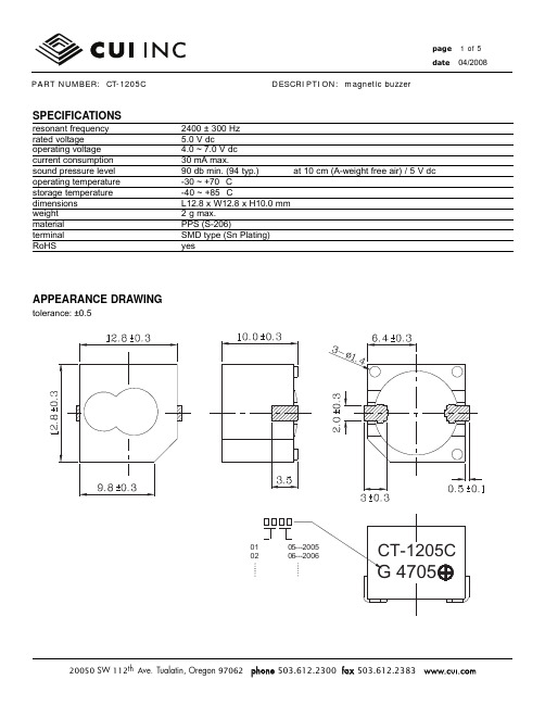
DESCRIPTION: magnetic buzzer PART NUMBER: CT-1205CSPECIFICATIONSresonant frequency2400 ± 300 Hzrated voltage 5.0 V dcoperating voltage 4.0 ~7.0 V dccurrent consumption30 mA max.sound pressure level90 db min. (94 typ.)at 10 cm (A-weight free air) / 5 V dc operating temperature-30~+70° Cstorage temperature -40 ~ +85° Cdimensions L12.8 x W12.8 x H10.0 mmweight 2 g max.material PPS(S-206)terminal SMD type (Sn Plating)RoHS yesAPPEARANCE DRAWINGDESCRIPTION: magnetic buzzerPART NUMBER: CT-1205CMECHANICAL CHARACTERISTICSitem test conditionsolderability Lead terminals are immersed in rosin for5 seconds and then immersed in solder bathof 270 ±5°C for 3 ±1 seconds.soldering heat resistance The buzzer follows the reflow temperaturecurve to test its reflow thermo stability. terminal mechanical strength Lead pads will be soldered onto the PCB, theforce of 9.8N (1.0kg) is applied behind the partfor 10 seconds.vibration The buzzer will be measured after applyinga vibration amplitude of 1.5 mm with 10 to55 Hz band of vibration frequency to each ofthe 3 perpendicular directions for 2 hours. drop test The part will be dropped from a height of75 cm onto a 40 mm thick wooden board 3times in 3 axes (X, Y, Z) for a total of 9 drops.evaluation standard95% of the lead pad surfaces must be covered with fresh solder (except the edge of the terminal). No interference in operation.No damage or cutting off.After the test, the part will meet specifications without any damage to its appearance. The SPL should be within ±10dB compared with the initial measurement.|VOLTAGE-SOUND PRESSURE LEVELVOLTAGE-CURRENT CONSUMPTIONDESCRIPTION: magnetic buzzer PART NUMBER: CT-1205CENVIRONMENT TESTRELIABILITY TESTitem test conditionoperating (life test) 1. Continuous life test:The part will be subjected to 72 hours ofcontinuous operation at +55°C with ratedvoltage applied.2. Intermittent life test:A duty cycle of 1 minute on, 1 minute off, aminimum of 10,000 times at room temp(+25 ±10°C) with rated voltage applied.evaluation standardAfter the test, the part will meet specifications without any damage to its appearance and performance. After 4 hours at 25°C, the SPL should be within ±10dB compared with the initial measurement..TEST CONDITIONSstandard test condition a) temperature: +5 ~+35°C b) humidity: 45 - 85%c) pressure: 860-1060 mbar judgement test condition a) temperature: +25 ±2°C b) humidity: 60 - 70%c) pressure: 860-1060 mbarDESCRIPTION: magnetic buzzerPART NUMBER: CT-1205CDESCRIPTION: magnetic buzzer PART NUMBER: CT-1205C。
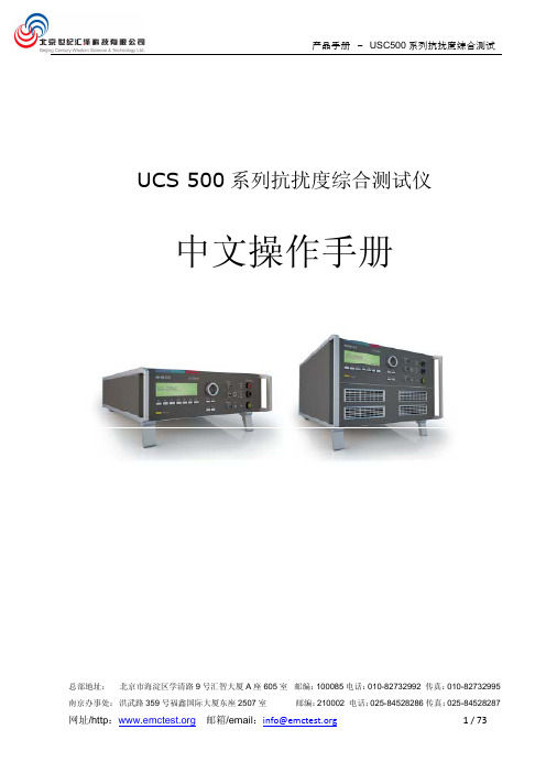
UCS 500N5 UCS 500N7系列抗扰度综合测试仪中文手册
3.1. 前面板.........................................................................................................7 3.2. 后面板.........................................................................................................9
产品手册 - USC500 系列抗扰度综合测试
UCS 500 系列抗扰度综合测试仪
中文操作手册
总部地址: 北京市海淀区学清路 9 号汇智大厦 A 座 605 室 邮编:100085 电话:010-82732992 传真:010-82732995
南京办事处: 洪武路 359 号福鑫国际大厦东座 2507 室
7.4.1. 工厂校准 .............................................................................................. 28 7.4.2. EMTEST 仪器校准周期指导 ....................................................................... 28
8. 交付件 ............................................................................................................. 29
8.1. 基本设备 .................................................................................................... 29 8.2. 附件和选件 ................................................................................................. 29
PSD-0505中文资料

Copyright PEAK electronics GmbH
Partnumbers
PART NO. INPUT VOLTAGE (VDC) INPUT CURRENT FULL LOAD OUTPUT VOLTAGE (VDC) OUTPUT CURRENT (max. mA) EFFICIENCY FULL LOAD (% TYP.)
PSD-3R305S PSD-053R3S PSD-0505S PSD-0509S PSD-0512S PSD-123R3S PSD-1205S PSD-1209S PSD-1212S PSD-1215S
3.3 5 5 5 5 12 12 12 12 12
450 171 246 254 252 73 100 105 103 100
5 3.3 5 9 12 3.3 5 9 12 15
200 200 200 110 84 200 200 110 84 67
70 77 81 78 80 75 81 78 81 83
元器件交易网
Telefon: +49 (0) 6135 931069 Telefax: +49 (0) 6135 931070 www.peak-eltronics.de
SMD SERIES
PSD-XXXXS 1KV ISOLATED 1W UNREGULATED SINGLE OUTPUT SMD
Ambient Temperature ° C 85
1.00 W
Pin # 1 3 7 8 14
Connection Single - V Input + V Input - V Output + V Output NC
CTA5中文资料

CIT RELAY™
CTA5
FEATURES: • Switching capacity up to 40A @ 14VDC • Small size and light weight • PCB pin mounting available • Suitable for automobile and lamp accessories • Two footprint styles available
GENERAL DATA
Electrical Life @ rated load Mechanical Life Insulation Resistance Dielectric Strength, Coil to Contact Contact to Contact Shock Resistance Vibration Resistance Terminal (Copper Alloy) Strength Operating Temperature Storage Temperature Solderability Weight 100K cycles, typical 10M cycles, typical 100MΩ min @ 500VDC 750V rms min. @ sea level 500V rms min. @ sea level 200m/s2 for 11ms 1.27mm double amplitude 10-40Hz 10N -40 °C to + 85 °C -40 °C to + 155 °C 230 °C ± 2 °C for 10 ± 0.5s 19g open. 21g covered
Rated
Max.
6 9 12 18 24
B1205中文版的资料

O u tp u t P o w e r (W )
5V & 12V Input
1.5
24V & 48V Input 70° c 85° c
1
0.5
0 -40° c
0° c
50° c
100° c
150° c
A m b ie n t T e m p e ra tu re ( C )
Industry standard来自pinoutSELECTION GUIDE
Input Order Code Voltage (V) B0505S-1W B0509S-1W B0512S-1W B0515S-1W B0524S-1W B1205S-1W B1209S-1W B1212S-1W B1215S-1W B2405S-1W B2409S-1W B2412S-1W B2415S-1W B4805S-1W B4809S-1W B4812S-1W B4815S-1W 5 5 5 5 5 12 12 12 12 24 24 24 24 48 48 48 48 Output Voltage (V) 5 9 12 15 24 5 9 12 15 5 9 12 15 5 9 12 15 Output Current (mA) 200 111 83 66 42 200 111 83 66 200 111 83 66 200 111 83 66 Input Current (Rated Load) (mA) 289 260 256 250 248 120 115 110 115 60 56 52 52 30 28 26 26 Efficiency % 70 77 78 80 80 69 74 76 72 70 75 80 80 70 75 80 80 Isolation Capacitance pF 48 37 33 40 48 33 48 55 48 40 59 78 79 32 50 76 75 MTTF1 kHrs 290 1173 633 360 290 620 488 360 488 201 185 163 136 213 194 164 140 SIP Package Style
ADS1205中文资料
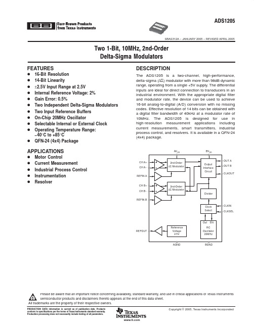
ESD damage can range from subtle performance degradation to complete device failure. Precision integrated circuits may be more susceptible to damage because very small parametric changes could cause the device not to meet its published specifications.Figure 20Frequency (kHz)02468101214161819Figure 21Frequency (kHz)02468101214161819EFFECTIVE NUMBER OF BITSvs DECIMATION RATIO1001k9886746250382614Sinc 2FilterSinc 3FilterPOWER−SUPPLY CURRENTvs TEMPERATURE40−2020406080100Temperature (_C)CLKSEL =1CLKSEL =0,CLKIN =20MHzCLKSEL =0,CLKIN =32MHzPACKAGING INFORMATIONOrderable Device Status (1)Package Type Package Drawing Pins Package Qty Eco Plan (2)Lead/Ball Finish MSL Peak Temp (3)ADS1205IRGER ACTIVE QFN RGE 243000Green (RoHS &no Sb/Br)CU NIPDAU Level-2-260C-1YEAR ADS1205IRGERG4ACTIVE QFN RGE 243000Green (RoHS &no Sb/Br)CU NIPDAU Level-2-260C-1YEAR ADS1205IRGET ACTIVE QFN RGE 24250Green (RoHS &no Sb/Br)CU NIPDAU Level-2-260C-1YEAR ADS1205IRGETG4ACTIVEQFNRGE24250Green (RoHS &no Sb/Br)CU NIPDAULevel-2-260C-1YEAR(1)The marketing status values are defined as follows:ACTIVE:Product device recommended for new designs.LIFEBUY:TI has announced that the device will be discontinued,and a lifetime-buy period is in effect.NRND:Not recommended for new designs.Device is in production to support existing customers,but TI does not recommend using this part in a new design.PREVIEW:Device has been announced but is not in production.Samples may or may not be available.OBSOLETE:TI has discontinued the production of the device.(2)Eco Plan -The planned eco-friendly classification:Pb-Free (RoHS)or Green (RoHS &no Sb/Br)-please check /productcontent for the latest availability information and additional product content details.TBD:The Pb-Free/Green conversion plan has not been defined.Pb-Free (RoHS):TI's terms "Lead-Free"or "Pb-Free"mean semiconductor products that are compatible with the current RoHS requirements for all 6substances,including the requirement that lead not exceed 0.1%by weight in homogeneous materials.Where designed to be soldered at high temperatures,TI Pb-Free products are suitable for use in specified lead-free processes.Green (RoHS &no Sb/Br):TI defines "Green"to mean Pb-Free (RoHS compatible),and free of Bromine (Br)and Antimony (Sb)based flame retardants (Br or Sb do not exceed 0.1%by weight in homogeneous material)(3)MSL,Peak Temp.--The Moisture Sensitivity Level rating according to the JEDEC industry standard classifications,and peak solder temperature.Important Information and Disclaimer:The information provided on this page represents TI's knowledge and belief as of the date that it is provided.TI basesits knowledge and belief on information provided by third parties,and makes no representation or warranty as to the accuracy of such information.Efforts are underway to better integrate information from third parties.TI has taken and continues to take reasonable steps to provide representative and accurate information but may not have conducted destructive testing or chemical analysis on incoming materials and chemicals.TI and TI suppliers consider certain information to be proprietary,and thus CAS numbers and other limited information may not be available for release.In no event shall TI's liability arising out of such information exceed the total purchase price of the TI part(s)at issue in this document sold by TI to Customer on an annual basis.PACKAGE OPTION ADDENDUM21-Jun-2005Addendum-Page 1元器件交易网IMPORTANT NOTICETexas Instruments Incorporated and its subsidiaries (TI) reserve the right to make corrections, modifications, enhancements, improvements, and other changes to its products and services at any time and to discontinue any product or service without notice. Customers should obtain the latest relevant information before placing orders and should verify that such information is current and complete. All products are sold subject to TI’s terms and conditions of sale supplied at the time of order acknowledgment.TI warrants performance of its hardware products to the specifications applicable at the time of sale in accordance with TI’s standard warranty. T esting and other quality control techniques are used to the extent TI deems necessary to support this warranty. Except where mandated by government requirements, testing of all parameters of each product is not necessarily performed.TI assumes no liability for applications assistance or customer product design. Customers are responsible for their products and applications using TI components. T o minimize the risks associated with customer products and applications, customers should provide adequate design and operating safeguards.TI does not warrant or represent that any license, either express or implied, is granted under any TI patent right, copyright, mask work right, or other TI intellectual property right relating to any combination, machine, or process in which TI products or services are used. Information published by TI regarding third-party products or services does not constitute a license from TI to use such products or services or a warranty or endorsement thereof. Use of such information may require a license from a third party under the patents or other intellectual property of the third party, or a license from TI under the patents or other intellectual property of TI.Reproduction of information in TI data books or data sheets is permissible only if reproduction is without alteration and is accompanied by all associated warranties, conditions, limitations, and notices. Reproduction of this information with alteration is an unfair and deceptive business practice. TI is not responsible or liable for such altered documentation.Resale of TI products or services with statements different from or beyond the parameters stated by TI for that product or service voids all express and any implied warranties for the associated TI product or service and is an unfair and deceptive business practice. TI is not responsible or liable for any such statements. Following are URLs where you can obtain information on other Texas Instruments products and application solutions:Products ApplicationsAmplifiers Audio /audioData Converters Automotive /automotiveDSP Broadband /broadbandInterface Digital Control /digitalcontrolLogic Military /militaryPower Mgmt Optical Networking /opticalnetwork Microcontrollers Security /securityTelephony /telephonyVideo & Imaging /videoWireless /wirelessMailing Address:Texas InstrumentsPost Office Box 655303 Dallas, Texas 75265Copyright 2005, Texas Instruments Incorporated。
PECcatalog(CCC中文)
熔断时间 最小 100 小时 0.75 秒 0.15秒 0.04 秒 0.02 秒 最大 ---1800 秒 5 秒 0.5 秒 0.2 秒
* 根据使用状况,保险丝特性可能改变.
额定电压 : 直流32V 电池间接耐久性 (周围温度 : 24℃)
在70%额定电流下循环了250000次满足性能要求。每个循环包括10秒开、10秒关的间断电流。
熔断时间 最小 100 小时 60 秒 2 秒 0.2 秒 0.04 秒 最大 ---1800 秒 60 秒 7 秒 1 秒
安培比率% 110% 135% 200% 350% 600%
* 根据使用状况,保险丝特性可能改变.
额定电压 : 直流32V 电池间接耐久性 (周围温度 : 24℃)
在50%额定电流下循环了10000次满足性能要求。每个循环包括5分钟开、10分钟关的间断电流。
在50%额定电流下循环了10000次满足性能要求。每个循环包括5分钟开、10分钟关的间断电流。
% 温度引起的容量变化
容量以 -0.14%/℃的比例变化
汽车零部件 汽车零部件
保险丝 延时保险丝 L型
12.0mm 8.0mm
熔断特性
41.0mm
延时保险丝目录
零部件 编号 3130 3140 3150 3160 3170 3180 3100 3110 3120 安培 比率(A) 30 40 50 60 70 80 100 125 150 外壳 颜色 橙 绿 红 黄 棕 白 蓝 粉红 灰
延时保险丝目录
零部件编号 3420 3430 3440 安培 比率(A) 20 30 40 外壳 颜色 浅蓝 粉红 绿
限时特性
(周围温度 : 24℃)
安培比率 % 110% 200% 350% 600%
4中文版ASME规范+第Ⅱ卷+D篇+材料性能+2005增补
A05 27 | 188 188 187 … 180 173 167 162 160 158
157 155 154 154 …
27 | …(17 个)
A05
新增加:
A05 28 | 27Ni-22Cr-7Mo-Mn-Cu-N 焊接管子 SA-249 …
S31277 … … 45 …
28 | 772 359 NP NP 427 NP NFN-26 …
原 B-250
原 B-260
导则 节号和条文 节号和条文
节号 节号 节号和条文 节号和条文
节号和条文
节号和条文
重新命名原‘非强制性附录 B’,并移到第 1 分篇;接在‘政策说明’之后、 表 1A 之前。标题,改为:
‘在应力表和在力学性能和物理性能表中查找材料的导则’
A05
改为:
1 序言
本导则旨在......。
......可返回去查阅 2.1 节中关于公称成分的讨论。
......相同的方式,可参见 2.2 节中的讨论。
改为:
2.6 表 4
......,分别再次参考 2.1 节和 2.2 节。
1.2
B-300
节号和 条文
改为: 3 力学性能表
...... 中的注解,3.1 节和 3.4 节提供了按每一张表的材料排列方式。
04 中文版 页码
章节
修改部位
05 增 补 修 改 内 容
新增加:
A05 31 | 27Ni-22Cr-7Mo-Mn-Cu-N 焊接公称管 SA-312 …
62-65 表 1A(续) 第 31 行
S31277 … … 4 5 … 31 | 772 359 NP NP 427 NP NFN-26 G3,G5 A05
丙戊酸钠和碳青霉烯类抗菌药物相互作用的临床观察

丙戊酸钠和碳青霉烯类抗菌药物相互作用的临床观察李娟;姜辉;魏金霞【摘要】目的评价丙戊酸钠和碳青霉烯类抗菌药合用相互作用的临床意义.方法收集7例症状性癫(癎)并发重症肺部感染患者应用丙戊酸钠和碳青霉烯类抗菌药治疗的临床资料,监测两药合用前、合用中及停止合用后丙戊酸血浓度.结果 4例患者合用丙戊酸钠和美罗培南期间丙戊酸血浓度明显下降,最低降至4.23 μg·mL-1,多在4~15 μg·mL-1之间,较应用美罗培南前下降40~70 μg·mL-1;1例患者同日开始应用丙戊酸钠和美罗培南,丙戊酸血浓度持续不达治疗窗;2例患者合用丙戊酸钠和亚胺培南/西司他丁期间丙戊酸血浓度无下降.结论丙戊酸钠和美罗培南合用短时间内血清丙戊酸浓度显著降低,临床上应避免二者联用;丙戊酸钠与亚胺培南/西司他丁合用未出现血清丙戊酸浓度下降,需进一步收集资料评估.%Objective To discuss the drug interaction between valproic acid (VPA) and carbapenem antibiotics (CP) in epileptic patients. Methods The clinical data of seven symptomatic epileptic patients with severe pneumonia treated with VPA and CP were analyzed retrospectively. The serum concentration of VPA was monitored before, during and after the combined use of VPA and CP. Results In four cases with combined use of VPA and meropenem, VPA was decreased significantly, with the level ranging from 4 to 15 μg o ml/-1 , which was 40-70 μg o ml/-1 lower than before the treatment. In one patient prescribed with VPA and meropenem at the same time, the serum concentration of VPA could not reach the therapeutic window. In two cases with concomitant use of VPA and imipenem, the serum level of VPA did not decrease. Conclusion Concomitant administration of VPA andmeropenem leads to a rapid decline in serum concentration of VPA. To avoid the recurrence of epileptic seizures, the concomitant administration of VPA and meropenem should be avoided in clinic. There is no decrease of serum concentration of VPA in the concomitant administration of VPA and imipenem, but more data are needed to demonstrate it.【期刊名称】《医药导报》【年(卷),期】2012(031)010【总页数】3页(P1364-1366)【关键词】丙戊酸;抗菌药,碳青霉烯类;美罗培南;亚胺培南/西司他丁;癫(癎),症状性【作者】李娟;姜辉;魏金霞【作者单位】广州军区武汉总医院干部病房一科,430070;广州军区武汉总医院干部病房一科,430070;广州军区武汉总医院干部病房一科,430070【正文语种】中文【中图分类】R971.6;R978近年来越来越多的文献报道,癫患者合用丙戊酸钠和碳青霉烯类抗菌药物时出现丙戊酸(valproic acid,VPA)血浓度急剧下降、甚至癫发作的情况。
DIR9001中文资料

BurrĆBrown Productsfrom TexasInstrumentsFEATURES APPLICATIONSDESCRIPTIONDIR9001SLES198–DECEMBER2006 96-kHz,24-Bit Digital Audio Interface Receiver•AV/DVD Receiver,AV Amplifier•One-Chip Digital Audio Interface Receiver(DIR)Including Low-Jitter Clock-Recovery•Car or Mobile Audio SystemSystem•Digital Television•Compliant With Digital Audio Interface•Musical InstrumentsStandards:IEC60958(former IEC958),JEITA•Recording SystemsCPR-1205(former EIAJ CP-1201,CP-340),•High-End Audio/Sound Card for PCAES3,EBU tech3250•Replacement of DIR1703•Clock Recovery and Data Decode From•Other Applications Requiring S/PDIF Receiver Biphase Input Signal,Generally Called S/PDIF,EIAJ CP-1201,IEC60958,AES/EBU•Biphase Input Signal Sampling Frequency(f S)The DIR9001is a digital audio interface receiver that Range:28kHz to108kHzcan receive a28-kHz to108-kHz sampling-•Low-Jitter Recovered System Clock:50ps frequency,24-bit-data-word,biphase-encoded signal.The DIR9001complies with IEC60958-3,JEITA •Jitter Tolerance Compliant With IEC60958-3CPR-1205(Revised version of EIAJ CP-1201),•Selectable Recovered System Clock:128f S,AES3,EBUtech3250,and it can be used in various 256f S,384f S,512f Sapplications that require a digital audio interface.•Serial Audio Data Output Formats:24-Bit I2S;The DIR9001supports many output system clock MSB-First,24-Bit Left-Justified;MSB-First16-,and output data formats and can be used flexibly in 24-Bit Right-Justifiedmany application systems.As the all functions which •User Data,Channel-Status Data Outputs the DIR9001provides can be controlled directly Synchronized With Decoded Serial Audio Data through control pins,it can be used easily in anapplication system that does not have a •No External Clock Required for Decodemicrocontroller.Also,as dedicated pins are provided •Includes Actual Sampling Frequencyfor the channel-status bit and user-data bit, Calculator(Needs External24.576-MHz Clock)processing of their information can be easily•Function Control:Parallel(Hardware)accomplished by connecting with a microcontroller,DSP,etc.•Functions Similar and Pin AssignmentsEquivalent to Those of DIR1703The DIR9001does not require an external clocksource or resonator for decode operation if the •Single Power Supply:3.3V(2.7V to3.6V)internal actual-sampling-frequency calculator is not •Wide Operating Temperature Range:–40°C toused.Therefore,it is possible to reduce the cost of a 85°Csystem.•5V-Tolerant Digital InputsThe operating temperature range of the DIR9001is •Package:28-pin TSSOP,Pin Pitch:0,65mm specified as–40°C to85°C,which makes it suitablefor automotive applications.Please be aware that an important notice concerning availability,standard warranty,and use in critical applications of TexasInstruments semiconductor products and disclaimers thereto appears at the end of this data sheet.SpAct is a trademark of Texas Instruments.All other trademarks are the property of their respective owners.PRODUCTION DATA information is current as of publication date.Copyright©2006,Texas Instruments Incorporated Products conform to specifications per the terms of the TexasInstruments standard warranty.Production processing does notnecessarily include testing of all parameters.RECOMMENDED OPERATING CONDITIONSDIR9001SLES198–DECEMBER 2006This integrated circuit can be damaged by ESD.Texas Instruments recommends that all integrated circuits be handled with appropriate precautions.Failure to observe proper handling and installation procedures can cause damage.ESD damage can range from subtle performance degradation to complete device failure.Precision integrated circuits may be more susceptible to damage because very small parametric changes could cause the device not to meet its published specifications.over operating free-air temperature range (unless otherwise noted)(1)VALUEUNIT V CC Supply voltage–0.3to 4V V DDV CC to V DD Supply voltage differences ±0.1V AGND to DGNDGround voltage differences ±0.1V Digital input –0.3to 6.5Digital input voltage V Digital output –0.3to (V DD +0.3)<4XTI,XTO –0.3to (V CC +0.3)<4Analog input voltageV FILT–0.3to (V CC +0.3)<4Input current (any pins except supplies)±10mA Ambient temperature under bias –40to 125°C Storage temperature –55to 150°C Junction temperature 150°C Lead temperature (soldering)260°C,5s Package temperature (reflow,peak)260°C(1)Stresses beyond those listed under absolute maximum ratings may cause permanent damage to the device.These are stress ratings only and functional operation of the device at these or any other conditions beyond those indicated under recommended operating conditions is not implied.Exposure to absolute-maximum-rated conditions for extended periods may affect device reliability.over operating free-air temperature range (unless otherwise noted)MINNOM MAX UNIT V CC Analog supply voltage 2.7 3.3 3.6VDC V DDDigital supply voltage 2.73.3 3.6VDC XTI is connected to clock source 24.576MHz Digital input clock frequencyXTI is connected to DGNDNot requiredMHz Digital output load capacitance,except SCKO 20pF Digital output load capacitance (SCKO)10pF T AOperating free-air temperature–4085°C2Submit Documentation FeedbackELECTRICAL CHARACTERISTICSDIR9001 SLES198–DECEMBER2006All specifications at TA =25°C,VDD=VCC=3.3V(unless otherwise noted)PARAMETER TEST CONDITIONS MIN TYP MAX UNIT DIGITAL INPUT/OUTPUT CHARACTERISTICSV IH0.7V DD V DD Input logic level(1)VDCV IL0.3V DDV IH2 5.5 Input logic level(2)VDCV IL0.8V OH I O=4mA0.85V DDOutput logic level(3)VDCV OL I O=–4mA0.15V DDI IH V IN=V DD65100Input leakage current(4)µAI IL V IN=0V–1010I IH V IN=V DD–1010Input leakage current(5)µAI IL V IN=0V–100–65I IH V IN=V DD–1010Input leakage current(6)µAI IL V IN=0V–1010BIPHASE SIGNAL INPUT AND PLLInput sampling frequency range28108kHzJitter tolerance—(IEC60958-3)IEC60958-3(2003-01)CompliantFrom biphase signal detection to error-outPLL lock-up time100msrelease(ERROR=L)RECOVERED CLOCK AND DATASerial audio data width1624Bit128f S 3.58413.824256f S7.16827.648 SCKO frequency MHz384f S10.75241.472512f S14.33655.296 BCKO frequency64f S 1.792 6.912MHz LRCKO frequency f S28108kHzf S=48kHz,SCKO=256f S,measuredSCKO jitter50100ps rmsperiodicSCKO duty cycle45%55%XTI SOURCE CLOCKXTI is connected to clock source24.576 XTI source clock frequency MHzNotXTI is connected to DGNDrequired Frequency accuracy XTI is connected to clock source–100100ppmXTI input-clock duty cycle XTI is connected to clock source45%55%POWER SUPPLY AND SUPPLY CURRENTV CC 2.7 3.3 3.6 Operation voltage range VDCV DD 2.7 3.3 3.6(1)CMOS compatible input:XTI(not5-V tolerant)(2)5-V tolerant TTL inputs:RXIN,FMT0,FMT1,PSCK0,PSCK1,CKSEL,RST,RSV(3)CMOS outputs:XTO,SCKO,BCKO,LRCKO,DOUT,UOUT,COUT,BFRAME,ERROR,CLKST,AUDIO,EMPH,FSOUT0,FSOUT1(4)Internal pulldowns:FMT0,FMT1,PSCK0,PSCK1,CKSEL,RSV(5)Internal pullup:RST(6)No internal pullup and pulldown:RXIN,XTI3Submit Documentation FeedbackPIN ASSIGNMENTSDIR9001(TOP VIEW)DIR9001SLES198–DECEMBER 2006ELECTRICAL CHARACTERISTICS (continued)All specifications at T A =25°C,V DD =V CC =3.3V (unless otherwise noted)PARAMETERTEST CONDITIONSMINTYP MAX UNIT f S =96kHz,PLL locked,XTI connected 68.3mA to DGNDI CCSupply current (7)f S =96kHz,PLL locked,XTI connected 68.3mA to 24.576-MHz resonator RXIN =H or L,XTI =L,RST =L 130µA f S =96kHz,PLL locked,XTI connected 68.3mA to DGNDI DDSupply current (7)f S =96kHz,PLL locked,XTI connected 912.4mA to 24.576-MHz resonator RXIN =H or L,XTI =L,RST =L 72µA f S =96kHz,PLL locked,XTI connected 4055mW to DGNDP DPower dissipation (7)f S =96kHz,PLL locked,XTI connected 5068mW to 24.576-MHz resonator RXIN =H or L,XTI =L,RST =L0.67mWTEMPERATURE RANGE T A Operation temperature range –4085°C θJA Thermal resistance28-pin T-SSOP105°C/W(7)No load connected to SCKO,BCKO,LRCKO,DOUT,COUT,VOUT,BFRAME,FSOUT0,FSOUT1,CLKST,ERROR,EMPH,AUDIO4Submit Documentation FeedbackDIR9001SLES198–DECEMBER2006 TERMINAL FUNCTIONSTERMINAL PULLI/O REMARKS DESCRIPTIONUP/DOWNNAME NO.AGND23–Analog groundAUDIO1OUT CMOS Channel-status data information of non-audio sample word,active-low BCKO11OUT CMOS Audio data bit clock outputBFRAME18OUT CMOS Indication of top block of biphase input signalCKSEL28IN Pulldown5-V tolerant TTL Selection of system clock source,Low:PLL(VCO)clock,High:XTI clock(1) CLKST9OUT CMOS Clock change/transition signal outputCOUT15OUT CMOS Channel-status data serial output synchronized with LRCKODGND6–Digital groundDOUT12OUT CMOS16-bit/24-bit decoded serial digital audio data outputEMPH17OUT CMOS Channel-status data information of pre-emphasis(50µs/15µs)ERROR27OUT CMOS Indication of internal PLL or data parity errorFILT22–External filter connection terminal;must connect recommended filter.FMT025IN Pulldown5-V tolerant TTL Decoded serial digital audio data output format selection0(1)FMT126IN Pulldown5-V tolerant TTL Decoded serial digital audio data output format selection1(1)FSOUT02OUT CMOS Actual sampling frequency calculated result output0FSOUT13OUT CMOS Actual sampling frequency calculated result output1LRCKO10OUT CMOS Audio data latch enable outputPSCK013IN Pulldown5-V tolerant TTL PLL source SCKO output frequency selection0(1)PSCK114IN Pulldown5-V tolerant TTL PLL source SCKO output frequency selection1(1)RST21IN Pullup5-V tolerant TTL Reset control input,active-low(2)RSV19IN Pulldown Reserved,must be connected to DGND(1)RXIN20IN5-V tolerant TTL Biphase digital data input(3)SCKO4OUT CMOS System clock outputUOUT16OUT CMOS User data serial output synchronized with LRCKOV CC24–Analog power supply,3.3-VV DD5–Digital power supply,3.3-VCMOSXTI8IN Oscillation amplifier input,or external XTI source clock inputSchmitt-triggerXTO7OUT CMOS Oscillation amplifier output(1)TTL Schmitt-trigger input with internal pulldown(51kΩtypical),5-V tolerant(2)TTL Schmitt-trigger input with internal pullup(51kΩtypical),5-V tolerant(3)TTL Schmitt-trigger input,5-V tolerant.5Submit Documentation FeedbackBLOCK DIAGRAMSCKOBCKOLRCKODOUTFSOUT0FSOUT1CLKST EMPHUOUT COUT BFRAME CKSEL ERROR AUDIO V DDDGNDAGNDV CCDIR9001SLES198–DECEMBER 20066Submit Documentation FeedbackTYPICAL PERFORMANCE CHARACTERISTICSPOWER SUPPLY CURRENTf S − Sampling Frequency − kHz 6810121416182030405060708090100I C C + I D D − S u p p l y C u r r e n t − m AG001f S − Sampling Frequency − kHz6810121416182030405060708090100I C C + I D D − S u p p ly C u r r e n t − m AG002RECOVERED SYSTEM CLOCK (SCKO)JITTERf S − Sampling Frequency − kHz2040608010012014016018020030405060708090100P e r i o d i c J i t t er − p s r m sG003DIR9001SLES198–DECEMBER 2006Oscillation amplifier operating with crystal;1-kHz,0-dB,sine-wave data;no loadSUPPLY CURRENTSUPPLY CURRENTvsvsLOCKED SAMPLING FREQUENCYLOCKED SAMPLING FREQUENCYFigure 1.Figure 2.SCKO JITTERvsLOCKED SAMPLING FREQUENCYFigure 3.7Submit Documentation FeedbackDEVICE INFORMATIONACCEPTABLE BIPHASE INPUT SIGNAL AND BIPHASE INPUT PIN (RXIN)DIR9001SLES198–DECEMBER 2006The DIR9001can decode the biphase signal format which is specified in one of the following standards.Generally,these following standards may be called Sony/Philips digital interface format (S/PDIF)or AES/EBU.•IEC60958(revised edition of former IEC958)•JEITA CPR-1205(revised edition of former EIAJ CP-1201,CP-340)•AES3•EBU tech3250The sampling frequency range and data word length which DIR9001can decode is as follows:•Sampling frequency range is 28kHz to 108kHz.•Maximum audio sample word length is 24-bit.Note of others about the biphase input signal.•The capture ratio of the built-in PLL complies with level III of sampling frequency accuracy (±12.5%),which is specified in IEC60958-3.•The jitter tolerance of the DIR9001complies with IEC60958-3.•The PLL may also lock in outside of the specified sampling-frequency range,but extended range is not assured.Notice about the signal level and transmission line of the biphase input signal.•The signal level and the transmission line (optical,differential,single-ended)are different in each standard.•The biphase input signal is connected to the RXIN pin of the DIR9001.•The RXIN pin has a 5-V tolerant TTL-level input.•An optical receiver module (optical to electric converter)such as TOSLINK,which is generally used in consumer applications,is connected directly to the RXIN pin without added external components.•The output waveform of the optical receiver module varies depending on the characteristics of each product type,so a dumping resistor or buffer amplifier might be required between the optical receiver module output and the DIR9001input.Careful handling is required if the optical receiver module and the DIR9001are separated by a long distance.•The DIR9001needs an external amplifier if it is connected to a coaxial transmission line.•The DIR9001needs an external differential to single-ended converter,attenuator,etc.,for general consumer applications if non-optical transmission line is used.8Submit Documentation Feedback SYSTEM RESETV DD 2.7VRST DIR9001StatusDIR9001SLES198–DECEMBER2006 DEVICE INFORMATION(continued)The DIR9001reset function is controlled by and external reset pin,RST.The reset operation must be performed during the power-up sequence as shown in Figure4.Specifically,the DIR9001requires reset operation with a100-ns period after the supply voltage risesFigure4.Required System Reset TimingThe state of each output pins during reset is shown in Table1.Table1.Output-Pin States During Reset PeriodCLASSIFICATION PIN NAME WHILE RST=LBCKO LClock LRCKO LSCKO LData DOUT LAUDIO LBFRAME LCLKST LCOUT LFlag and status EMPH LERROR HFSOUT0LFSOUT1LUOUT LOscillation amplifier XTO Output9Submit Documentation FeedbackOPERATION MODE AND CLOCK TRANSITION SIGNAL OUTOperation ModeDIR9001SLES198–DECEMBER 2006The DIR9001has the following three operation modes.These modes are selected by the connection of the CKSEL pin.•PLL MODE:For demodulating a biphase input signal;always outputs PLL source clock •XTI MODE:For clock generator;always outputs XTI source clock•AUTO MODE:Automatic clock source selection;output source depends on ERROR pin.Notes about operation mode selection:•Normally,the PLL mode:CKSEL =L is selected to decode a biphase input signal.•The XTI mode is a mode that supplies the XTI source clock to peripheral devices (A/D converters,etc);therefore,recovered clock and decoded data is not output.•When the XTI source is not used,an XTI source is not required.In this case,clocks are not output in the XTI mode.•At the time of XTI mode selection,biphase decode function continues to operate.Therefore,the biphase input status (ERROR)and the result of the sampling frequency calculator (a required XTI source for operation),are always monitored.That is,the following output pins:ERROR,BFRAME,FSOUT[1:0],CLKST,AUDIO and EMPH are always enabled.The details of these three modes are given in Table 2.Table 2.Operation Mode and Clock SourceOPERATION CKSEL PIN ERROR DOUT DATAAUDIO FSOUT BFRAMECOUT SCKO,BCKO,LRCKO MODESETTINGPIN EMPH [1:0]UOUT CLOCK SOURCE STATUSHPLL (VCO)free-runningMUTE (Low)LOW HL LOW LOW clock (1)PLLLLPLL recovered clockDecoded data OUT OUT OUT OUT H XTI clock MUTE (Low)LOW HL LOW LOW XTI H L XTI clock MUTE (Low)OUT OUT OUT LOW H XTI clock MUTE (Low)LOW HL LOW LOW Connected to AUTO ERROR pinLPLL recovered clockDecoded dataOUTOUTOUTOUT(1)The VCO free-running frequency is not a constant frequency,because the VCO oscillation frequency is dependent on supply voltage,temperature,and process variations.10Submit Documentation FeedbackSCKOBCKOLRCKODOUTRXINFSOUT0FSOUT1CLKST CKSEL ERROR Clock Transition Signal OutDIR9001SLES198–DECEMBER 2006Figure 5.Clock Source,Source Selector,and Data PathThe DIR9001provides an output pulse that is synchronized with the PLL’s LOCK/UNLOCK status change.The CLKST pin outputs the PLL status change between LOCK and UNLOCK.The CLKST output pulse depends only on the status change of the PLL.This clock change/transition signal is output through CLKST.As this signal indicates a clock transition period due to a PLL status change,it can be used for muting or other appropriate functions in an application.A clock source selection caused by the CLKSEL pin does not affect the output of CLKST.CLKST does change due to PLL status change even if CKSEL =H in the XTI source mode.When DIR9001is reset in the state where it is locked to the biphase input signal,the pulse signal of CLKST is not output.That is,the priority of reset is higher than CLKST.The relation among the lock-in/unlock process,the CLKST and ERROR outputs,the output clocks (SCKO,BCKO,LRCKO),and data (DOUT)is shown in Figure 6.11Submit Documentation FeedbackDIR9001 StatusNote:means clock source change.DIR9001SLES198–DECEMBER 2006PARAMETERSMIN TYP MAX UNIT t CLKSTCLKST pulse duration,high420µsFigure 6.Lock-In and Unlock Process12Submit Documentation FeedbackCLOCK DESCRIPTION System Clock SourceDIR9001 SLES198–DECEMBER2006DIR9001has the following two clock sources for the system clock.•PLL source(128f S,256f S,384f S,512f S are available,recovered by built-in PLL)•XTI source(One24.576-MHz resonator or external clock source is required.)Two clock sources are used for the following purpose.•PLL source:Recovered system clock from the biphase input signal•XTI source:Clock source for peripheral devices(for example,A/D converter,microcontroller,etc.) Measurement reference clock for the internal actual-sampling-frequency calculatorDescription of PLL clock source•The PLL clock source is the output clock of built-in PLL(including VCO).•The PLL clock source frequency is selectable from128f S,256f S,384f S,512f S by PSCK[1:0].•When the PLL is in the locked condition,the PLL clock source is the clock recovered from the biphase input signal.•When PLL is in the unlocked condition,the PLL clock source is the built-in free-running clock of the VCO.•The frequency of the PLL clock source in the unlocked condition is not constant.(The VCO free-running frequency is dependent on supply voltage,temperature,and variations in the die’s wafer.)Description of XTI clock source•The XTI clock source is not used to recover the clock and decode data from the biphase input signal.•Therefore,if the DIR9001is used only for recovering the clock and decoding data from the biphase input signal,an XTI clock source is not required.In this case,the XTI pin must be connected to the DGND pin.(The DIR9001does not have a selection pin for using an XTI clock source or not using one.)The selection method of clock source•The output clock is selected from two clock sources by the level of the CKSEL pin.•The selection of the system clock source depends only on the input level of CKSEL pin.•CKSEL=L setting is required for recovering the clock and decoding data from biphase input.•CKSEL=H setting is required for XTI clock source output.•The continuity of clock during the clock source transition between the XTI source and the PLL source is not assured.Method of automatic clock source selection(CLOCK SOURCE MODE:AUTO)•This method enables selection of the clock source automatically,using the DIR9001ERROR status.The PLL source clock is output when ERROR=L;the XTI source is output when ERROR=H.•To enable automatic clock source selection,the CKSEL pin must be connected to the ERROR pin.•If XTI clock source is needed during the ERROR period,this method is recommended.•Because the clock source during ERROR status is XTI,if an XTI clock source is not provided to the XTI pin, then SCKO,BCKO,and LRCKO are not output during the ERROR period.The relationship between the clock/data source and the combination of CKSEL pin and PLL status inputs is shown in Table2.The clock tree system is shown in Figure7.13Submit Documentation FeedbackSCKO (O)BCKO (O)LRCKO (O)XTI (I)XTO (O)RXINCKSEL (I)PLL Clock Source (Built-In PLL and VCO)DescriptionDIR9001SLES198–DECEMBER 2006Figure 7.Clock Tree DiagramThe DIR9001has on-chip PLL (including VCO)for recovering the clock from the biphase input signal.The clock that is output from the built-in VCO is defined as the PLL clock source.In the locked state,the built-in PLL generates a system clock that synchronizes with the biphase input signal.In the unlocked state,the built-in PLL (VCO)generates a free-running clock.(The frequency is not constant.)The PLL can support a system clock of 128f S ,256f S ,384f S ,or 512f S ,where f S is the sampling frequency of the biphase input signal.The system clock frequency of the PLL is selected by PSCK[1:0].The DIR9001can decode a biphase input signal through its 28sampling-frequency range of kHz to 108kHz,independent of the setting of PSCK[1:0].Therefore,the DIR9001can decode a biphase input signal with a sampling frequency from 28kHz to 108kHz at all settings of PSCK[1:0]The relationship between the PSCK[1:0]selection and the output clock (SCKO,BCKO,LRCKO)from the PLL source is shown in Table 3.Table 3.SCKO,BCKO,and LRCKO Frequencies Set by PSCK[1:0]PSCK[1:0]SETTING OUTPUT CLOCK FROM PLL SOURCE PSCK1PSCK0SCKO BCKO LRCKO L L 128f S 64f S f S L H 256f S 64f S f S H L 384f S 64f S f S HH512f S64f Sf S14Submit Documentation FeedbackRequired PLL Loop Filter DescriptionDIR9001 SLES198–DECEMBER2006In PLL mode(CKSEL=L),output clocks(SCKO,BCKO,LRCKO)are generated from the PLL source clock. The relationship between frequencies of LRCKO,BCKO,and SCKO at different sampling frequencies f S of the biphase input signal are shown in Table4.Table4.Output Clock Frequency in PLL Locked State(CKSEL=L) LRCKO BCKO SCKO(Depending on PSCK[1:0]Setting)f S64f S128f S256f S384f S512f S32kHz 2.048MHz 4.096MHz8.192MHz12.288MHz16.384MHz44.1kHz 2.8224MHz 5.6448MHz11.2896MHz16.9344MHz22.5792MHz48kHz 3.072MHz 6.144MHz12.288MHz18.432MHz24.576MHz88.2kHz 5.6448MHz11.2896MHz22.5792MHz33.8688MHz45.1584MHz96kHz 6.144MHz12.288MHz24.576MHz36.864MHz49.152MHzThe DIR9001incorporates a PLL for generating a clock synchronized with the biphase input signal.The built-in PLL requires an external loop filter,which is specified as follows.Operation and performance is assured for recommended filter components R1,C1,and C2.Notes about Loop Filter Components and Layout•The resistor and capacitors which comprise the filter should be located and routed as close as possible to the DIR9001.•A carbon film resistor or metal film resistor,with tolerance less than5%,is recommended.•Film capacitors,with tolerance is less than5%,is recommended.•If ceramic capacitors are used for C1and C2,parts with a low voltage coefficient and low temperature coefficient,such as CH or C0G,are recommended.•The external loop filter must be placed on FILT pins.•The GND node of the external loop filter must be directly connected with the AGND pin of the DIR9001;it must be not combined with other signals.The configuration of external loop filter and the connection with the DIR9001is shown in Figure8.Figure8.Loop Filter ConnectionThe recommended values of loop filter components is shown in Table5.Table5.Recommended Value of Loop Filter ComponentsREF.NO.RECOMMENDED VALUE PARTS TYPE TOLERANCER1680ΩMetal film or carbon≤5%C10.068µF Film or ceramic(CH or C0G)≤5%C20.0047µF Film or ceramic(CH or C0G)≤5%15Submit Documentation Feedback XTI Clock Source and Oscillation Amplifier DescriptionResonator Connection ExternalClockExternal Clock Input ConnectionDIR9001SLES198–DECEMBER2006This clock,driven by the built-in oscillation amplifier or input into the XTI pin from an external clock,is defined as the XTI source.A24.576-MHz fundamental resonator or external24.576-MHz clock is used as the XTI source. The DIR9001requires an XTI source for following purposes:•The measurement reference clock of actual-sampling-frequency calculator•The clock source for the XTI source mode(CKSEL=H setting)(That is,the DIR9001does not require an XTI source if it is only decoding the biphase input signal.)The XTI clock source is supplied in one of the following two ways;the details are described in Figure9.•Setting up an oscillation circuit by connecting a resonator with the built-in amplifier•Applying a clock from an external oscillator circuit or oscillator moduleTo set up an oscillation circuit by connecting a resonator with the built-in amplifier:•Connect a24.576-MHz resonator between the XTI pin and XTO pin.•The resonator should be a fundamental-mode type.•A crystal resonator or ceramic resonator can be used.•The load capacitor C L1,C L2,and the current-limiting resistor R d depend on the characteristics of the resonator.•No external feedback resistor between the XTI pin and XTO pin is required,as an appropriate resistor is incorporated in the device.•No load other than the resonator is allowed on the XTO pin.To connect an external oscillator circuit or oscillator module:•Provide a24.576-MHz clock on the XTI pin•Note that the XTI pin is not5-V tolerant;it is simple CMOS input.•The XTO pin must be open.Figure9.XTI and XTO Connection DiagramDescription of oscillation amplifier operation:•The built-in oscillation amplifier is always working.•If the XTI source clock is not used,then the XTI pin must be connected to DGND.•For reducing power dissipation,it is recommended to not use the XTI source clock.In XTI mode(CKSEL=H),output clocks(SCKO,BCKO,LRCKO)are generated from XTI source clock.The relation between output clock frequency(SCKO,BCKO,LRCKO)and the XSCK pin setting in XTI source mode is shown in Table6.Table6.SCKO,BCKO,LRCKO Output Frequency at XTI ModeXTI FREQUENCY OUTPUT CLOCK FREQUENCY IN XTI SOURCE MODE(CKSEL=H)SCKO BCKO LRCKO24.576MHz24.576MHz 6.144MHz96kHz16Submit Documentation FeedbackDATA DESCRIPTIONDecoded Serial Audio Data Output and Interface FormatBiphase Signal (IN)BFRAME (OUT)LRCKO (OUT)(I S)2LRCKO (OUT)(Except I S)2DOUT (OUT)DIR9001SLES198–DECEMBER 2006The DIR9001supports following 4-data formats for the decoded data.•16-bit,MSB-first,right-justified •24-bit,MSB-first,right-justified •24-bit,MSB-first,left-justified •24-bit,MSB-first,I 2SDecoded data is MSB first and 2s-complement in all formats.The decoded data is provided through the DOUT pin.The format of the decoded data is selected by the FMT[1:0]pins.The data formats for each FMT[1:0]pin setting are shown in Table 7.Table 7.Serial Audio Data Output Format Set by FMT[1:0]FMT[1:0]SETTINGS DOUT SERIAL AUDIO DATA OUTPUT FORMATFMT1FMT0L L 16-bit,MSB-first,right-justified L H 24-bit,MSB-first,right-justified H L 24-bit MSB-first,left-justifiedHH24-bit,MSB-first,I 2SPARAMETERSMIN TYP MAX UNIT t LATELRCKO/DOUT latency3/f SsFigure tency Time Between Biphase Input and LRCKO/DOUT17Submit Documentation Feedback。
RCLAMP0521P中文资料
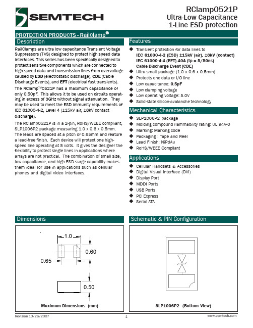
Typical 9.3
Maximum 5 11
Units V V
0.025
1
µA
15
V
25
V
0.30
0.50
pF
2007 Semtech Corp.
2
元器件交易网
RClamp0521P
Clamping Voltage - VC (V)
PROTECTION PRODUCTS Typical Characteristics
Mechanical Characteristics
SLP1006P2 package Molding compound flammability rating: UL 94V-0 Marking: Marking code Packaging : Tape and Reel Lead Finish: NiPdAu RoHS/WEEE Compliant
90 80 70 60 50 40 30 20 10
0 0
Power Derating Curve
25
50
75
100
125
150
Ambient Temperature - TA (oC)
Clamping Voltage vs. Peak Pulse Current
24 22 20 18 16 14 12 10
10 MHz
100 MHz
13 GHz GHz
START. 030 MHz
STOP 3000.000000 MHz
3
元器件交易网
PROTECTION PRODUCTS Applications Information
SDC1205资料
1. Appearance : No significant abnormality 2. Inductance change : Within ±20%
Preheating 260°C Dipping
Natural
cooling
Preheat : 150°C, 60sec. Solder : Sn-Ag3.0-Cu0.5 Solder Temperature : 260±5°C Flux for lead free : rosin Dip Time : 10±0.5sec.
IDC (A) Max. 8.00 7.00 6.00 5.00 4.40 4.20 4.00 3.50 3.30 3.00 2.80 2.30 2.10 2.00 1.80 1.70 1.50 1.40 1.30 1.10 1.00 0.90 0.80 0.75 0.68 0.65 0.58 0.54 0.48 0.43 0.40
元器件交易网
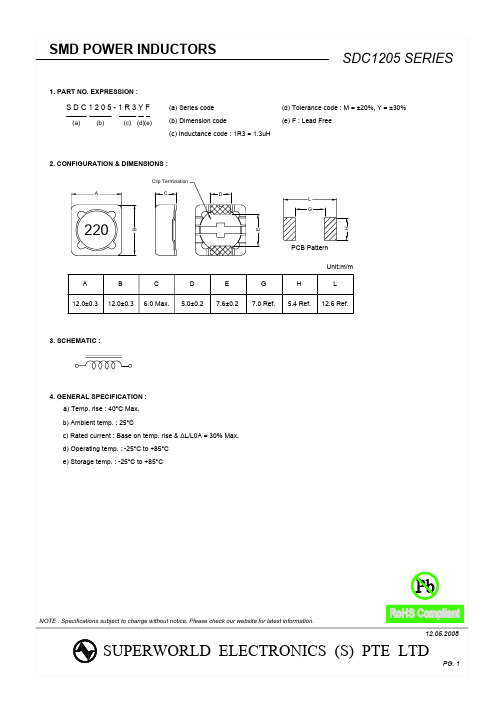
SMD POWER INDUCTORS
7. SOLDERIND AND MOUNTING : 7-1. Recommended PC Board Pattern
12.6 7.0
SDC1205 SERIES
7-2. Soldering Mildly activated rosin fluxes are preferred. The minimum amount of solder can lead to damage from the stresses caused by the difference in coefficients of expansion between solder, chip and substrate. Our terminations are suitable for all wave and re-flow soldering systems. If hand soldering cannot be avoided, the preferred technique is the utilization of hot air soldering tools. 7-2.1 Solder Re-flow : Recommended temperature profiles for re-flow soldering in Figure 1. 7-2.2 Soldering Iron (Figure 2) : Products attachment with soldering iron is discouraged due to the inherent process control limitations. In the event that a soldering iron must be employed the following precautions are recommended. Note : a) Preheat circuit and products to 150°C. b) 280°C tip temperature (max) c) Never contact the ceramic with the iron tip d) 1.0mm tip diameter (max) e) Use a 20 watt soldering iron with tip diameter of 1.0mm f) Limit soldering time to 3 secs.
科瑞爱特 CT1200 通信电源 技术手册说明书
深圳市科瑞爱特科技开发有限公司CT1200系列技术说明书深圳市科瑞爱特科技开发有限公司地址:深圳市南山区创业路怡海广场西座8H 联系电话:************* 26521348 26521458传真:*************E-mail:****************敬告用户1.安装使用之前必须有专业人员在仔细阅读本说明书(带▲的说明文字尤其需仔细阅读)后才能进行安装工作。
2.如有不会引起用户安装使用方面误解的部分设计细节的改动,恕不另行通知。
第一部分CT1200(48V/15A/20A)开关电源技术参数CT1200(48V/15A)开关电源(以下简称开关电源)是我公司采用新型的移相控制软开关技术生产的电源,具有体积小重量轻效率高可靠性好的特点。
1.工作环境条件工作环境温度:-5℃—40℃环境相对湿度:≤90%2.交流输入电压范围:165VAC±5VAC—265VAC±5VAC 50HZ±5HZ3.直流输出电压:均充状态时直流输出电压为54.3V浮充状态时直流输出电压为52.7V▲均充电压与浮充电压在出厂前已设定好,一般情况下不允许用户自行调整。
如要调整,必须在专业人员或厂家技术人员的指导下调整。
▲用户如需特殊规格的开关电源请另行通知厂家。
4.直流输出电流:额定输出电流:15A(20A)最大输出电流(限流值):15.5A(20A)5.主要技术指标稳压精度:<0.5%衡重杂音:≤2mV峰峰杂音:≤200mV浪涌电流:≤6A软启动时间:3—8秒6.告警保护交流输入过压保护:265V±5V(关机,自动恢复)交流输入欠压保护:165V±5V(关机,自动恢复)直流输出过压保护:≥60V±1V(关机,人工恢复)直流输出欠压(电池欠压)保护:≤45V±0.5V直流输出限流保护:15.5A(20A)直流输出短路保护:短路电流≤2A,短路取消后自动恢复第二部分性能简介1.均充/浮充转换功能当按入此按钮时开关电源处于均充工作状态,均充电压值出厂时设定为54.3V。
帕顿1205RC用户手册说明书

SALES OFFICE(301) 975-1000TECHNICAL SUPPORT(301) 975-1007An ISO-90011.0 WARRANTY INFORMATIONPatton Electronics warrants all Model 1205RC components to be free from defects, and will—at our option—repair or replace the product should it fail within one year from the first date of shipment.This warranty is limited to defects in workmanship or materials, and does not cover customer damage, abuse or unauthorized modifi-cation. If this product fails or does not perform as warranted, your sole recourse shall be repair or replacement as described above. Under no condition shall Patton Electronics be liable for any damages incurred by the use of this product. These damages include, but are not limited to, the following: lost profits, lost savings and incidental or consequen-tial damages arising from the use of or inability to use this product. Patton Electronics specifically disclaims all other warranties, expressed or implied, and the installation or use of this product shall be deemed an acceptance of these terms by the user.1.1 RADIO AND TV INTERFERENCEThe Model 1205RC generates and uses radio frequency energy, and if not installed and used properly—that is, in strict accordance with the manufacturer’s instructions—may cause interference to radio and television reception. The Model 1205RC has been tested and found to comply with the limits for a Class A computing device in accordance with the specifications in Subpart J of Part 15 of FCC rules, which are designed to provide reasonable protection from such interference in a commercial installation. However, there is no guarantee that interfer-ence will not occur in a particular installation. If the Model 1205RC does cause interference to radio or television reception, which can be determined by turning the power off or removing the card, the user is encouraged to try to correct the interference by one or more of the fol-lowing measures: moving the computing equipment away from the receiver, re-orienting the receiving antenna and/or plugging the receiv-ing equipment into a different AC outlet (such that the computing equip-ment and receiver are on different branches).In the event the user detects intermittent or continuous product malfunction due to nearby high power transmitting radio frequency equipment, the user is strongly advised to take the following steps: use only data cables with an exter-nal outer shield bonded to a metal or metalized connector; and, config-ure the rear card as shown in section 3.4 of this manual.1.2 CE NOTICEThe CE symbol on your Patton Electronics equipment indicates that it is in compliance with the Electromagnetic Compatibility (EMC) directive and the Low Voltage Directive (LVD) of the Union European (EU). A Certificate of Compliance is available by contacting Technical Support.1All warranty and nonwarranty repairs must be returned freight pre-paid and insured to Patton Electronics. All returns must have a Return Materials Authorization number on the outside of the shipping contain-er. This number may be obtained from Patton Electronics Technical Support: (301) 975-1007; ; or, support@. Packages received without an RMA number will not be accepted.Patton Electronics' technical staff is also available to answer any questions that might arise concerning the installation or use of your Model 1205RC. Technical Service hours: 8AM to 5PM EST, Monday through Friday.22.0 GENERAL INFORMATIONThank you for your purchase of this Patton Electronics product. This product has been thoroughly inspected and tested and is warrant-ed for One Year parts and labor. If any questions during installation or use of the 1205RC, contact Patton Electronics Technical Support: (301) 975-1007; ; or, ******************.2.1 FEATURES• V.35 (EIA-530) operation• Synchronous data rates from 32 to 144 Kbps• Host-to-host distances up to 300 feet• Internal or external clocking• All necessary data, clocking and control signals supported• Constant or RTS controlled carrier selections• RTS-CTS delay options of 0mS, 7mS or 53mS• Front panel LEDs show TD, DTR and CD activity for each port • Two UD-26 connectors on rear interface card• Switchable 120V or 240V power supply• Mounts in Patton’s 16-slot rack chassis and 2/4/8-slot ClusterBoxes• Made in the U.S.A.2.2 DESCRIPTIONThe Patton Model 1205RC synchronous modem eliminator rack card lets two synchronous hosts communicate with each other in the same room for a fraction of the cost of a pair of high speed modems. Supporting synchronous data rates of 32, 48, 56, 64, 72, 112, 128 and 144 Kbps, the Model 1205RC can be configured to emu-late dial-up or leased line service. Maximum distance between the connected hosts is 300 feet. Timing can be set for internal or external clock, and all necessary data, clocking and control signals are support-ed.The Model 1205RC is designed to mount in Patton’s 2U high, 16-slot rack chassis, as well as Patton’s 2/4/8-slot desktop Cluster Boxes. This rack chassis and cluster boxes feature a switchable 120/240 VAC power supply (optional 48 VDC) and hot swappable function/interface cards mounted in a mid-plane architecture. Front panel LEDs show TD, DTR and CD activity for both ports, as well as power. The rear interface card has two UD-26 connectors for patching to the host devices.3The power supply on/off switch is located on the front panel. When plugged in and switched on, a red front panel LED will glow. Since the Model 1000R16 is a “hot swappable” rack, it is not necessary for any cards to be installed before switching on the power supply.The power supply may be switched off at any time without harming the installed cards.NOTE: Please refer to the Model 1000RP Series User Manual AC and DC Rack Mount Power Supplie s for fuse and power cardreplacement information.4.2 INSTALLING THE MODEL1205RC INTO THE CHASSISThe Model 1205RC is comprised of a front card and a rear card. The two cards meet inside the rack chassis and plug into each other by way of mating 50 pin card edge connectors. Use the following steps as a guideline for installing each Model 1205RC into the rack chassis:1.Slide the rear card into the back of the chassis along themetal rails provided.2.Secure the rear card using the metal screws provided.3.Slide the card into the front of the chassis. It should meet therear card when it’s almost all the way into the chassis.4.Push the front card gently into the card-edge receptacle of therear card. It should “click” into place.5.Secure the front card using the thumb screws.NOTE:Since the Model 1000R16 chassis allows “hot swapping”of cards, it is not necessary to power down the rack when youinstall or remove a Model 1205RC.10There is no power switch on the Model 1205RC: Power is auto-matically applied to the 1205RC when its card-edge connector makes contact with the chassis’mid-plane socket, or when the chassis’power supply is turned on. Note: The 1205RC is a “hot swappable” card—it will not be damaged by plugging it in or removing it while the rack is powered up.When the Model 1205RC is powered up, and both ports are pass-ing data normally, the following LED conditions will exist:• PWR = green• TD = blinking red and green• CD = green• DTR = green13APPENDIX AMODEL1205RC SPECIFICATIONSTransmission Format: Synchronous, CCITT V.35Internal Interface:Connection to Model 1000R16 rackchassis via male card edge External Interface:UD-26 female, ports A1 and B1Data Rates:32, 48, 56, 64, 72, 112, 128 and 144 Kbps Clocking:Internal, external or receive loopback Distance:300 feet (DTE to DTE)RTS/CTS Delay:Strap selectable, 0, 7, 53 mS (+/- 15%) Indicators: Independent Bi-color LED indicators foreach port: TD, CD and DTR; common“Power” indicatorTemperature:0-50°C / 32-122°FHumidity: 5 to 95%, noncondensingDimensions: 0.95”w x 3.1”h x 5.4”l14Dear Valued Customer,Thank you for purchasing Patton Electronics products! We doappreciate your business. I trust that you find this user manual helpful.We manufacture one of the widest selections of data communica-tions products in the world including CSU/DSU's, network termination units, powered and self-powered short range modems, fiber optic modems, interface converters, baluns, electronic data switches, data-line surge protectors, multi-plexers, transceivers, hubs, print servers and much more. We produce these products at our Gaithersburg, MD, USA, facility, and can custom manufacture products for your unique needs.We would like to hear from you. Please contact us in any of the fol-lowing ways to tell us how you like this product and how we can meet your product needs today and in the future.Web: Sales E-mail: ****************Support E-mail: ******************Phone - Sales (301) 975-1000Phone - Support (301) 975-1007Fax: (301) 869-9293Mail: Patton Electronics Company7622 Rickenbacker DriveGaithersburg, MD 20879 USAWe are committed to a quality product at a quality price. Patton Electronics is ISO 9001 certified. We meet and exceed the highest standards in the industry (CE, UL, etc.).It is our business to serve you. If you are not satisfied with any aspect of this product or the service provided from Patton Electronics or its distributors, please let us know.Thank you.Burton A.PattonExecutive Vice PresidentP.S. Please tell us where you purchased this product._________________________________________________________ _________________________________________________________ _________________________________________________________ __________________________________________________________________________________________________________________。
Reference solution, Part Number 5190-0545说明书
Reference solution, Part Number 5190-0545CHEMTREC®: 4001-204937化学品安全技术说明书GHS化学品标识应急咨询电话(带值班时间)::供应商/ 制造商:Agilent Technologies Shanghai Co., Ltd.CALC-AP412 Ying Lun RoadWaigaoqiao Free Trade Zone Shanghai 200131 P. R. China Reference solution, Part Number 5190-0545化学品的推荐用途和限制用途5190-0545产品号:物质用途:分析化学。
3 瓶 x 30 ml (5190-0545-1)安全技术说明书根据 GB/ T 16483-2008 和 GB/ T 17519-2013危险性类别信号词:警告危险性说明::防范说明预防措施:事故响应:如戴隐形眼镜并可方便地取出,取出隐形眼镜。
继续冲洗。
P337 + P313 - 如仍觉眼刺激: 求医/就诊。
安全储存:废弃处置:GHS标签要素象形图物质或混合物的分类根据 GB13690-2009 和 GB30000-2013严重眼损伤/眼刺激 - 类别 2B 危害水生环境一急性危险 - 类别 1H410危害水生环境一长期危险 - 类别 1紧急情况概述液体。
白色。
无资料。
有关环境保护措施,请参阅第 12 节。
物理和化学危险:物理状态:颜色:气味:与物理,化学和毒理特性有关的症状皮肤接触食入吸入没有具体数据。
没有具体数据。
没有具体数据。
:::眼睛接触:不利症状可能包括如下情况:刺激流泪充血发红延迟和即时影响,以及短期和长期接触引起的慢性影响短期暴露潜在的即时效应:无资料。
潜在的延迟效应:无资料。
潜在的即时效应:无资料。
长期暴露潜在的延迟效应:无资料。
环境危害:其他危害:没有已知信息。
没有出现就供应商当前所知可应用的浓度,被分类为对健康或环境有害及因此需要在本节报告的添加剂。
高镍三元材料烧结温度研究

高镍三元材料烧结温度研究佚名【摘要】研究了不同烧结温度下对高镍正极材料Li(Ni0.90Co0.05Mn0.05)0.998Zr0.002O2形貌、结构以及电化学性能的影响.XRD和SEM结果表明:不同烧结温度下合成的Li(Ni0.90Co0.05Mn0.05)0.998Zr0.002O2材料均为α-NaFeO2型层状结构,且随着烧结温度的增加,一次颗粒尺寸逐渐增大.740℃烧结温度下合成材料性能最优,首次放电比容量为210.8m A h/g,首次效率为89.1%,45℃下50圈循环保持率为93.44%.【期刊名称】《信息记录材料》【年(卷),期】2019(020)006【总页数】4页(P41-44)【关键词】锂离子电池;高镍三元材料;烧结温度;电化学性能【正文语种】中文【中图分类】TQ151 引言锂离子电池具有工作电压高、能量密度高、循环寿命长、质量轻、体积小、自放电率低、无记忆效应、环保等优点,被认为是可充电电池中最具吸引力的选择。
在过去的几十年中,锂离子电池广泛应用于小型电子设备,包括手机、笔记本电脑和摄像机[1] 。
LiCoO2层状材料作为一种有前途的商业应用材料,已得到广泛应用。
然而,钴的毒性和高成本限制了它的进一步发展[2] 。
具有层状结构的正极材料LiNi1-x-yCoxMnyO2不仅继承了其良好的LiCoO2循环性能,LiNiO2的高比电容和LiMn2O4的热稳定性,而且还具有低毒,低成本等优点[3] 。
高镍正极材料Li(Ni0.90Co0.05Mn0.05)0.998Zr0.002O2具有较高的比容量(>200mA·h/g)和良好的循环稳定性,具有很大潜力作为电动汽车使用的大容量电池的正极材料。
本文研究了烧结温度对锆掺杂改性的高镍三元材料性能的影响,便于精确掌握材料性能的影响因素及规律,确定材料合成工艺,为后续Li(Ni0.90Co0.05Mn0.05)0.998Zr0.002O2材料的工业化生产提供技术支持。
- 1、下载文档前请自行甄别文档内容的完整性,平台不提供额外的编辑、内容补充、找答案等附加服务。
- 2、"仅部分预览"的文档,不可在线预览部分如存在完整性等问题,可反馈申请退款(可完整预览的文档不适用该条件!)。
- 3、如文档侵犯您的权益,请联系客服反馈,我们会尽快为您处理(人工客服工作时间:9:00-18:30)。
DESCRIPTION: magnetic buzzer
PART NUMBER: CT-1205
current consumption 40 mA max.applying rated voltage, 2400 Hz square wave, ½ duty coil resistance
45.0 Ω±6.7
sound pressure level 87 db min. (92 typ.)at 10 cm (A-weight), applying rated voltage, 2400 Hz square wave, ½ duty
operating temperature -30~+85° C storage temperature -40 ~ +85° C
dimensions L12.8 x W12.8 x H7.1 mm weight 2 g
material PPS (S-206)
terminal SMD type (Sn Plating)RoHS
yes
APPEARANCE DRAWING
DESCRIPTION: magnetic buzzer
PART NUMBER: CT-1205
MECHANICAL CHARACTERISTICS
item
test condition
solderability
Lead terminals are immersed in solder bath of 270 ±5°C for 3 ±1 seconds.
soldering heat resistance The buzzer follows the reflow temperature curve to test its reflow thermo stability.
terminal mechanical strength
Lead pads will be soldered onto the PCB, the force of 9.8N (1.0kg) is applied behind the part for 10 seconds.
vibration
The buzzer will be measured after applying a vibration amplitude of 1.5 mm with 10 to 55 Hz band of vibration frequency to each of the 3 perpendicular directions for 2 hours.drop test
The part will be dropped from a height of 75 cm onto a 40 mm thick wooden board 3 times in 3 axes (X, Y , Z) for a total of 9 drops.
evaluation standard
95% of the lead pad surfaces
must be covered with fresh solder (except the edge of the terminal).No interference in operation.
No damage or cutting off.After the test, the part will meet specifications without any
damage to its appearance. The SPL should be within ±10dB compared with the initial measurement.
DESCRIPTION: magnetic buzzer PART NUMBER: CT-1205
ENVIRONMENT TEST
RELIABILITY TEST
item test condition
operating (life test) 1. Continuous life test:
The part will be subjected to 72 hours of
continuous operation at +70°C with 5 V,
2400 Hz applied.
2. Intermittent life test:
A duty cycle of 1 minute on, 1 minute off, a
minimum of 10,000 times at room temp
(+25 ±10°C) with 5 V, 2400 Hz applied.evaluation standard
After the test, the part will meet specifications without any damage to its appearance and performance. After 4 hours at 25°C, the SPL should be within ±10dB compared with the initial measurement.
TEST CONDITIONS
standard test condition a) temperature: +5 ~+35°C b) humidity: 45 - 85%c) pressure: 860-1060 mbar judgement test condition a) temperature: +25 ±2°C b) humidity: 60 - 70%c) pressure: 860-1060 mbar
DESCRIPTION: magnetic buzzer PART NUMBER: CT-1205
DESCRIPTION: magnetic buzzer PART NUMBER: CT-1205
PACKAGING。