MBR30020CT中文资料
MBR2060CT;MBR2050CT;MBR2045CT;MBR2035CT;中文规格书,Datasheet资料
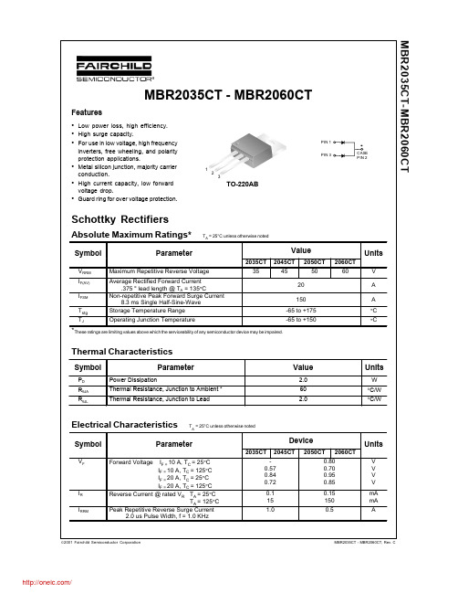
MBR2035CT - MBR2060CT
Features • • • • • •
Low power loss, high efficiency. High surge capacity. For use in low voltage, high frequency inverters, free wheeling, and polarity protection applications. Metal silicon junction, majority carrier conduction. High current capacity, low forward voltage drop. Guard ring for over voltage protection.
20
150 125 100 75 50 25 0
16
12
SINGLE PHASE HALF WAVE 60HZ RESISTIVE OR INDUCTIVE LOAD .375" (9.00mm) LOAD LENGTHS
8
4
0
0
25
50 75 100 125 Ambient Temperature [ºC]
Figure 3. Forward Voltage Characteristics
Figure 4. Reverse Current vs Reverse Voltage
2000 1000 500
MBR2050CT-MBR2060CT MBR2035CT-MBR2045CT
Transient Thermal Impedance [ºC/W]
Thermal Characteristics
MBR10200CT-MBR20100CT ASEMI高压肖特基二极管规格
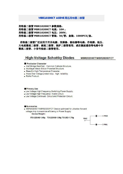
MBR10200CT ASEMI高压肖特基二极管
肖特基二极管MBR10200CT参数规格:
肖特基二极管MBR10200CT电流:10A;
肖特基二极管MBR10200CT电压:200V;
肖特基二极管MBR10200CT管装:50/管;盒装:1000PCS/盒。
肖特基二极管广泛应用于开关电源、变频器、驱动器等电路,作高频、低压、大电流整流二极管、续流二极管、保护二极管使用,或在微波通信等电路中作整流二极管、小信号检波二极管使用。
MBR10200CT ITO-220AB肖特基二极管PDF资料
MBR10200CT肖特基类型:高结温芯片,品牌:ASEMI,
应用市场:电源,小家电,LED电源,各式充电器,开关电源,LED显示屏等。
MBR10200CT肖特基相关参数如下:
MBR10200CT电压Vrrm:200V
MBR10200CT电流If平均:10A
MBR10200CT正向电压Vf最大:0.87V
MBR10200CT电流,Ifs最大:150A
MBR10200CT工作温度范围:-40°C to+150°C
MBR10200CT封装形式:TO-220/TO-220F/ITO-220
MBR10200CT反向恢复电流,Irrm:10UA
肖特基系列型号:
MBR1040CT,MBR1045CT,MBR1060CT,MBR1060FCT, MBR10100CT,MBR10100FCT,MBR10150FCT,MBR10150CT, MBR10200FCT,MBR10200CT
肖特基二极管封装:TO-251,TO-252,TO-263,
TO-220,TO-247,TO-3P。
MBR30H100CT中文资料
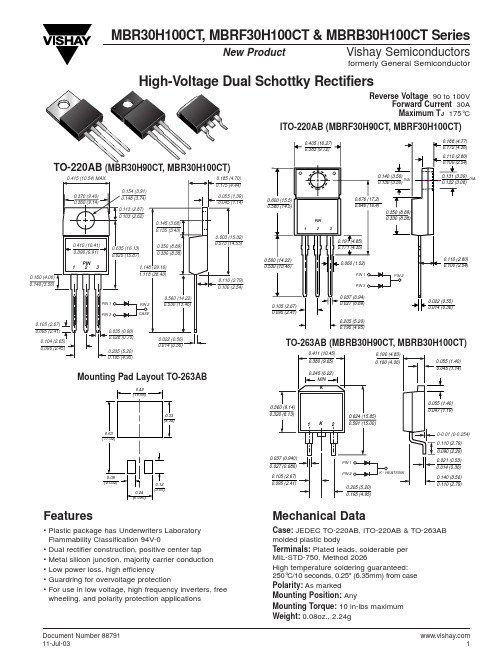
MBR30H100CT , MBRF30H100CT & MBRB30H100CT SeriesVishay Semiconductorsformerly General SemiconductorDocument Number New ProductReverse Voltage 90 to 100VForward Current 30A Maximum T J 175°CMounting Pad Layout TO-263ABITO-220AB (MBRF30H90CT, MBRF30H100CT)(MBR30H90CT, MBR30H100CT)TO-263AB (MBRB30H90CT, MBRB30H100CT)Features• Plastic package has Underwriters Laboratory Flammability Classification 94V-0• Dual rectifier construction, positive center tap • Metal silicon junction, majority carrier conduction • Low power loss, high efficiency• Guardring for overvoltage protection• For use in low voltage, high frequency inverters, free wheeling, and polarity protection applicationsMechanical DataCase:JEDEC TO-220AB, ITO-220AB & TO-263AB molded plastic bodyTerminals:Plated leads, solderable per MIL-STD-750, Method 2026High temperature soldering guaranteed: 250°C/10 seconds, 0.25" (6.35mm) from case Polarity:As markedMounting Position: AnyMounting Torque:10 in-lbs maximum Weight:0.08oz., 2.24gMBR30H100CT , MBRF30H100CT & MBRB30H100CT SeriesVishay Semiconductorsformerly General Semiconductor Document Number 88791Maximum Ratings (TC= 25°C unless otherwise noted)ParameterSymbol MBR30H90CTMBR30H100CTUnit Maximum repetitive peak reverse voltage V RRM 90100V Working peak reverse voltage V RWM 90100V Maximum DC blocking voltageV DC 90100V Maximum average forward rectified current Total device 30(see fig. 1)Per leg I F(AV)15A Peak forward surge current8.3ms single half sine-wave superimposed I FSM 275A on rated load (JEDEC Method) per legPeak repetitive reverse current per leg at t p = 2µs, 1KH Z I RRM 1.0A Voltage rate of change (rated V R )dv/dt 10,000V/µs Operating junction and storage temperature range T J , T STG –65 to +175°C RMS Isolation voltage (MBRF type only) from terminals 4500(1)to heatsink with t = 1 second, RH ≤30%V ISOL3500(2)V1500(3)Electrical Characteristics (TC= 25°C unless otherwise noted)ParameterSymbolValue Unit at I F = 15A, T J = 25°C 0.82Maximum instantaneous at I F = 15A, T J = 125°C V F0.67Vforward voltage per leg (4)at I F = 30A, T J = 25°C 0.93at I F = 30A, T J = 125°C0.80Maximum reverse current per leg T J = 25°C 5.0µA at working peak reverse voltage (4)T J = 125°CI R6.0mAThermal Characteristics (TC= 25°C unless otherwise noted)ParameterSymbol MBR MBRF MBRB UnitTypical thermal resistance per legR θJC1.94.61.9OC/WNotes:(1) Clip mounting (on case), where lead does not overlap heatsink with 0.110” offset (2) Clip mounting (on case), where leads do overlap heatsink(3) Screw mounting with 4-40 screw, where washer diameter is ≤ 4.9 mm (0.19”)(4) Pulse test: 300µs pulse width, 1% duty cycleOrdering InformationProductCase Package CodePackage OptionMBR30H90CT - MBR30H100CT TO-220AB 45Anti-Static tube, 50/tube, 2K/carton MBRF30H90CT - MBRF30H100CT ITO-220AB 45Anti-Static tube, 50/tube, 2K/carton 3113” reel, 800/reel, 4.8K/cartonMBRB30H90CT - MBRB30H100CTTO-263AB45Anti-Static tube, 50/tube, 2K/carton81Anti-Static 13” reel, 800/reel, 4.8K/cartonMBR30H100CT , MBRF30H100CT & MBRB30H100CT SeriesVishay Semiconductorsformerly General SemiconductorDocument Number Ratings andCharacteristic Curves (T A = 25°C unless otherwise noted)100100.10.011.0J u n c t i o n C a p a c i t a n c e (p F )110100100100000.110Reverse Voltage (V)t, Pulse Duration (sec.)I F -- I n s t a n t a n e o u s F o r w a r d C u r r e n t (A )5101520253035Fig. 1 – Forward Derating CurvePer LegA v e r a g e F o r w a r d C u r r e n t (A )Fig. 2 – Maximum Non-Repetitive Peak Forward Surge Current Per Leg1000。
MBRP30045CT中文资料
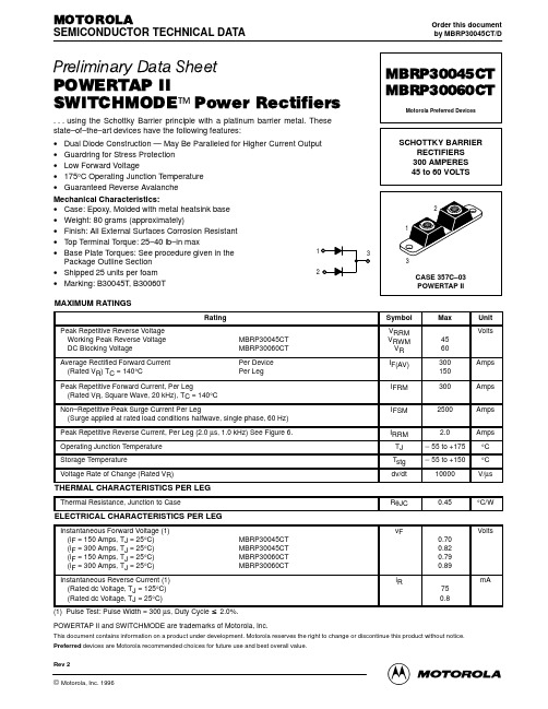
MOTOROLA
SEMICONDUCTOR TECHNICAL DATA
Order this document by MBRP30045CT/D
Preliminary Data Sheet
POWERTAP II SWITCHMODE™ Power Rectifiers
. . . using the Schottky Barrier principle with a platinum barrier metal. These state–of–the–art devices have the following features: • Dual Diode Construction — May Be Paralleled for Higher Current Output • Guardring for Stress Protection • Low Forward Voltage • 175°C Operating Junction Temperature • Guaranteed Reverse Avalanche Mechanical Characteristics: • Case: Epoxy, Molded with metal heatsink base • Weight: 80 grams (approximately) • Finish: All External Surfaces Corrosion Resistant • Top Terminal Torque: 25–40 lb–in max 1 • Base Plate Torques: See procedure given in the Package Outline Section 2 • Shipped 25 units per foam • Marking: B30045T, B30060T MAXIMUM RATINGS
MBRS10100CT资料
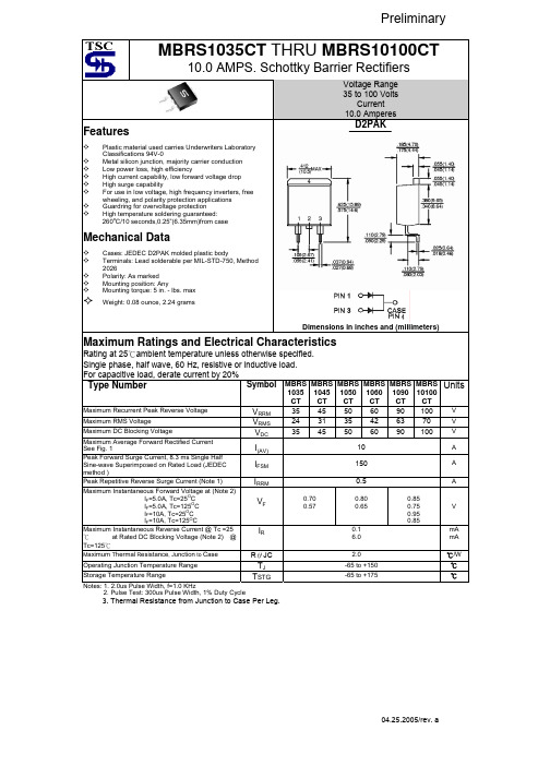
100
0.70 0.57 0.80 0.65 0.1 6.0 2.0 -65 to +150 -65 to +175 0.85 0.75 0.95 0.85
V mA mA ℃/W ℃ ℃
TSTG
TJ
3. Thermal Resistance from Junction to Case Per Leg.
04.25.2005/rev. a
元器件交易网
RATINGS AND CHARACTERISTIC CURVES (MBRS1035CT THRU MBRS10100CT)
FIG.1- FORWARD CURRENT DERATING CURVE
5.0
180
FIG.2- MAXIMUM NON-REPETITIVE FORWARD SURGE CURRENT PER LEG
Plastic material used carries Underwriters Laboratory Classifications 94V-0 Metal silicon junction, majority carrier conduction Low power loss, high efficiency High current capability, low forward voltage drop High surge capability For use in low voltage, high frequency inverters, free wheeling, and polarity protection applications Guardring for overvoltage protection High temperature soldering guaranteed: 260oC/10 seconds,0.25”(6.35mm)from case
SBR20100CT中文资料
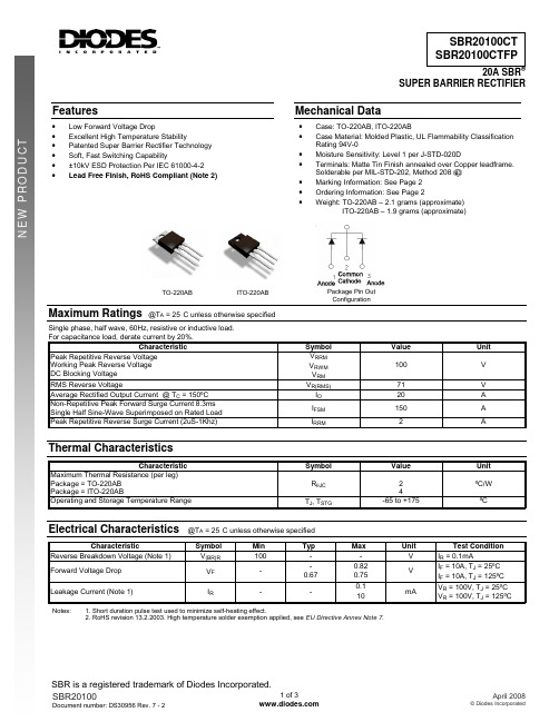
20A SBRSUPER BARRIER RECTIFIERFeatures• Low Forward Voltage Drop• Excellent High Temperature Stability• Patented Super Barrier Rectifier Technology • Soft, Fast Switching Capability• ±10kV ESD Protection Per IEC 61000-4-2 •Lead Free Finish, RoHS Compliant (Note 2)Mechanical Data• Case: TO-220AB, ITO-220AB• Case Material: Molded Plastic, UL Flammability Classification Rating 94V-0• Moisture Sensitivity: Level 1 per J-STD-020D• Terminals: Matte Tin Finish annealed over Copper leadframe. Solderable per MIL-STD-202, Method 208 • Marking Information: See Page 2 • Ordering Information: See Page 2• Weight: TO-220AB – 2.1 grams (approximate)ITO-220AB – 1.9 grams (approximate)Package Pin Out ConfigurationTO-220ABITO-220ABMaximum Ratings @T A = 25°C unless otherwise specifiedSingle phase, half wave, 60Hz, resistive or inductive load. For capacitance load, derate current by 20%.CharacteristicSymbol Value UnitPeak Repetitive Reverse Voltage Working Peak Reverse Voltage DC Blocking VoltageV RRM V RWM V RM 100 VRMS Reverse VoltageV R(RMS) 71 V Average Rectified Output Current @ T C = 150ºC I O 20 ANon-Repetitive Peak Forward Surge Current 8.3ms Single Half Sine-Wave Superimposed on Rated Load I FSM 150 APeak Repetitive Reverse Surge Current (2uS-1Khz) I RRM2 AThermal CharacteristicsCharacteristicSymbol Value Unit Maximum Thermal Resistance (per leg) Package = TO-220AB Package = ITO-220ABR θJC 2 4ºC/W Operating and Storage Temperature Range T J , T STG-65 to +175ºCElectrical Characteristics @T A = 25°C unless otherwise specifiedCharacteristicSymbol Min Typ Max Unit Test Condition Reverse Breakdown Voltage (Note 1) V (BR)R 100 - - V I R = 0.1mAForward Voltage Drop V F - - 0.67 0.82 0.75 VI F = 10A, T J = 25ºCI F = 10A, T J = 125ºCLeakage Current (Note 1)I R- - 0.1 10 mAV R = 100V, T J = 25ºCV R = 100V, T J = 125ºCNotes: 1. Short duration pulse test used to minimize self-heating effect.2. RoHS revision 13.2.2003. High temperature solder exemption applied, see EU Directive Annex Note 7.255075100125150175T C , CASE TEMPERATURE (°C)I F (A V E ), A V E R A G E F O R W A R D C U R R E N T (A )0.10.100.200.300.400.500.600.700.800.90V , INSTANTANEOUS FORWARD VOLTAGE (V)I , I N S T A N T A N E O U S F O R W A R D C U R R E N T (A )Figure 1: Current Derating Curve, Per ElementFigure 2: Typical Forward Characteristics, Per Element0.0010.010.111010020406080100V , INSTANTANEOUS REVERSE VOLTAGE (V)I , I N S T A N T A N E O U S R E V E R S E C U R R E N T (m A )Figure 3: Typical Reverse Characteristics, Per ElementOrdering Information (Note 3)Part Number Case PackagingSBR20100CT TO-220AB 50 pieces/tubeSBR20100CTFP ITO-220AB 50 pieces/tubeNotes:3. For packaging details, go to our website at /datasheets/ap02007.pdf.Marking InformationSBR20100CTFP = Product Type Marking CodeAB = Foundry and Assembly Code YYWW = Date Code MarkingYY = Last two digits of year, ex: 06 = 2006 WW = Week (01-52)SBR20100CT = Product Type Marking Code AB = Foundry and Assembly Code YYWW = Date Code Marking YY = Last two digits of year, ex: 06 = 2006 WW = Week (01-52)Package Outline DimensionsTO-220ABDim Min Typ MaxA 3.56 - 4.82 A1 0.51 - 1.39 A2 2.04 - 2.92 b 0.39 0.81 1.01 c 0.356 - 0.61 D 14.22 - 16.51D1 8.39 - 9.01e 2.54 e1 5.08E 9.66 - 10.66H1 5.85 - 6.85L 12.70 - 14.73L1 - - 6.35 P 3.54 - 4.08 Q 2.54 - 3.42 All Dimensions in mmITO-220AB (Note 4)Dim Min Typ Max A 4.50 4.70 4.90A1 3.04 3.243.44A2 2.56 2.762.96b 0.500.600.75b1 1.10 1.20 1.35c 0.500.600.70D 15.6715.8716.07D1 8.999.199.39e 2.54E 9.9110.1110.31L 9.459.7510.05L1 15.8016.0016.20P 2.98 3.18 3.38Q 3.10 3.30 3.50All Dimensions in mmITO-220AB ALTERNATE (Note 4)DIM. MIN. MAX. A 4.30 4.70 A1 1.3 b 0.50 0.75 b1 1.10 1.35 b2 1.50 1.75 c 0.50 0.75 D 14.80 15.20 E 9.96 10.36 e 2.54 typ F 2.80 3.20 J1 2.50 2.90 L 12.80 13.60 L1 1.70 1.90 L2 1.90 2.10 ØP 3.50 typ Q 2.70 typ All Dimensions in mmNotes:4. For product manufactured with Date Code 0733 (week 33, 2007) and newer, please refer to ITO-220AB dimensions. For product manufactured prior to Date Code 0733, please refer to ITO-220AB ALTERNATE dimensions.IMPORTANT NOTICEDiodes Incorporated and its subsidiaries reserve the right to make modifications, enhancements, improvements, corrections or other changes without further notice to any product herein. Diodes Incorporated does not assume any liability arising out of the application or use of any product described herein; neither does it convey any license under its patent rights, nor the rights of others. The user of products in such applications shall assume all risks of such use and will agree to hold Diodes Incorporated and all the companies whose products are represented on our website, harmless against all damages.LIFE SUPPORTDiodes Incorporated products are not authorized for use as critical components in life support devices or systems without the expressed written approval of the President of Diodes Incorporated.。
MBR30200CT台湾耐美肖特基三极管
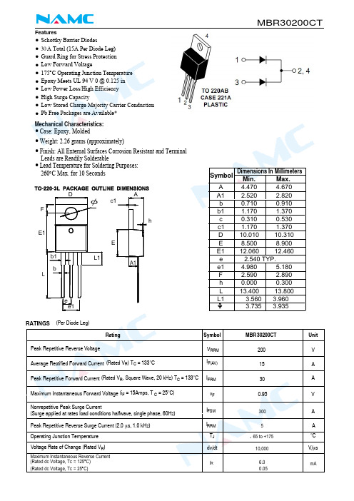
Features
• • • • • • • • • •
Schottky Barrier Diodes 30 A Total (15A Per Diode Leg) Guard Ring for Stress Protection Low Forward Voltage 175°C Operating Junction Temperature Epoxy Meets UL 94 V 0 @ 0.125 in Low Power Loss/High Efficiency High Surge Capacity Low Stored Charge Majority Carrier Conduction Pb Free Packages are Available*
260°C Max. for 10 Seconds
D
Leads are Readily Solderable
Symbol
A
Dimensions In Millimeters
O
F
I
c1 h
E1 E b1 b L L1
A1
e e1
A A1 b b1 c c1 D E E1 e e1 F h L L1 Φ
Maximum Instantaneous Reverse Current (Rated dc Voltage, TC = 125°C) (Rated dc Voltage, TC = 25°C)
Symbol VRRM IF(AV) IFRM vF IFSM IRRM TJ dv/dt
IR
MBR 30200CT 200 15 30 0.95
NUMBER OF CY CLES AT 6 0HZ
Fig.4 Max Non- Repetitive Surge Current
MBR20H200CT中文资料
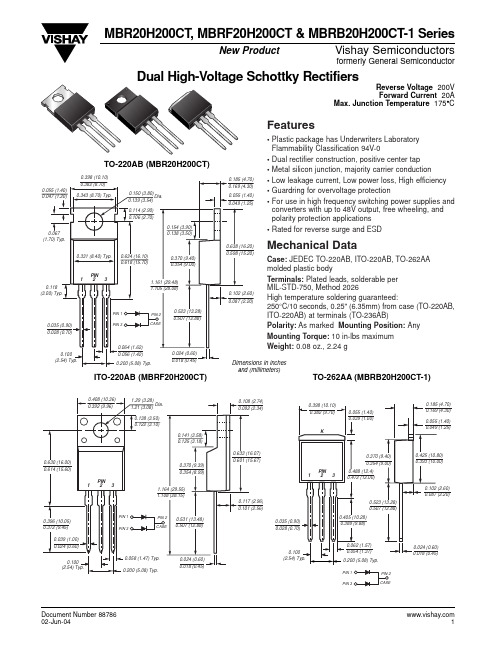
Features• Plastic package has Underwriters Laboratory Flammability Classification 94V-0• Dual rectifier construction, positive center tap • Metal silicon junction, majority carrier conductionPlated leads, solderable per As marked Mounting Position: Any 10 in-lbs maximum MBR20H200CT , MBRF20H200CT & MBRB20H200CT-1 SeriesVishay Semiconductorsformerly General SemiconductorDocument Number New ProductReverse Voltage 200V Forward Current 20AMax. Junction Temperature 175°CPIN 1PIN 3TO-220AB (MBR20H200CT)TO-262AA (MBRB20H200CT-1)Maximum Ratings (TC= 25°C unless otherwise noted)ParameterSymbol MBR20H200CT MBRF20H200CT MBRB20H200CT-1Unit Maximum repetitive peak reverse voltage V RRM 200V Working peak reverse voltage V RWM 200V Maximum DC blocking voltageV DC 200V Maximum average forward rectified current Total device 20(Fig. 1)Per leg I F(AV)10A Peak forward surge current8.3ms single half sine-wave superimposed I FSM 290A on rated load (JEDEC Method) per legPeak repetitive reverse current per leg at t p = 2µs, 1KH Z I RRM 1.0A Peak non-repetitive reverse surge energy E RSM 20mJ (8/20µs waveform)Non-repetitive avalanche energy per leg at 25°C, E AS = 2.0A, L=10mHE AS 20mJ Electrostatic discharge capacitor voltage Human body model: C = 100pF, R = 1.5K ΩV C 25KV Voltage rate of change (rated V R )dv/dt 10,000V/µs Operating junction and storage temperature range T J , T STG –65 to +175°C RMS Isolation voltage (MBRF type only) from terminals 4500(1)to heatsink with t = 1 second, RH ≤30%V ISOL3500(2)V1500 (3)Electrical Characteristics (TC= 25°C unless otherwise noted)ParameterSymbolTypical Maximum Unit Maximum instantaneous I F = 10A,T j = 25°C 0.810.88forward voltage per leg at:I F = 10A,T j = 125°C 0.650.75I F = 20A,T j = 25°C V F0.870.97V I F = 20A,T j = 125°C 0.740.85Maximum reverse current per leg T J = 25°C 5.0µA at working peak reverse voltage (4)T J = 125°CI R 1.0mA Typical junction capacitance at 4.0V, 1MHZCJ250pFThermal Characteristics (TC= 25°C unless otherwise noted)ParameterSymbol MBR MBRF MBRB Unit Typical thermal resistance per legR ΘJC2.04.02.0°C/WNotes:(1) Clip mounting (on case), where lead does not overlap heatsink with 0.110” offset (2) Clip mounting (on case), where leads does overlap heatsink(3) Screw mounting with 4-40 screw, where washer diameter is ≤ 4.9 mm (0.97”)(4) Pulse test: 300µs pulse width, 1% duty cycleOrdering InformationProduct Case Package CodePackage OptionMBR20H200CT TO-220AB 45Anti-Static tube, 50/tube, 1K/carton MBRF20H200CT TO-200AB 45Anti-Static tube, 50/tube, 1K/carton MBRB20H200CT-1TO-262AA45Anti-Static tube, 50/tube, 1K/cartonMBR20H200CT , MBRF20H200CT & MBRB20H200CT-1 SeriesVishay Semiconductorsformerly General Semiconductor Document Number 88786MBR20H200CT , MBRF20H200CT & MBRB20H200CT-1 SeriesVishay Semiconductorsformerly General SemiconductorDocument Number 0.10.30.20.40.60.8 1.00.50.70.9 1.1100100.110.10.011101001,0000.011100100.1Fig. 3 – Typical Instantaneous Forward CharacteristicsI R -- I n s t a n t an e o u s R e v e r s e C u r r e n t (µA )J u n c t i o n C a p a c i t a n c e (p F )1101001001000100000.110Reverse Voltage (V)102030507010040608090Fig. 4 – Typical ReverseCharacteristicsFig. 6 – Typical Transient Thermal Impedance Per Legt -- Pulse Duration (sec.)Instantaneous Forward Voltage (V)Percent of Rated Peak Reverse Voltage (%)I F -- I n s t a n t a n e o u s F o r w a r d C u r r e n t (A )510152025255075100125150175A v e r a g e F o r w a r d C u r r e n t (A )Case T emperature (°C)0255075100125150175200225250275300325110100A v e r a g e F o r w a r d C u r r e n t (A )Number of Cycles at 60 H ZFig. 5 – Typical Junction CapacitanceFig. 1 – Forward Derating CurveFig. 2 – Maximum Non-Repetitive Peak Forward Surge Current35010,000Ratings andCharacteristic Curves (T A = 25°C unless otherwise noted)。
MBRB20200CT中文资料
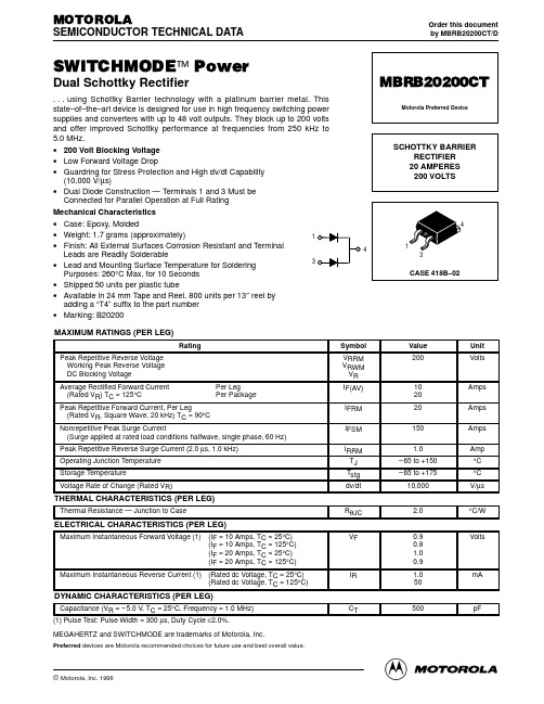
ELECTRICAL CHARACTERISTICS (PER LEG)
Maximum Instantaneous Forward Voltage (1) 0.9 0.8 1.0 0.9 1.0 50 Volts
Maximum Instantaneous Reverse Current (1) (Rated dc Voltage, TC = 25°C) (Rated dc Voltage, TC = 125°C)
Amps Amps Amps Amp °C °C V/µs °C/W
THERMAL CHARACTERISTICS (PER LEG)
Thermal Resistance — Junction to Case RθJC (IF = 10 Amps, TC = 25°C) (IF = 10 Amps, TC = 125°C) (IF = 20 Amps, TC = 25°C) (IF = 20 Amps, TC = 125°C) VF 2.0
150
160
Figure 3. Forward Power Dissipation
IF(AV), AVERAGE FORWARD CURRENT (AMPS) 20 500
Figure 4. Current Derating, Case
RθJA = 16°C/W RATED VOLTAGE C, CAPACITANCE (pF)
Figure 2. Typical Reverse Current (Per Leg)
SQUARE WAVE
RATED VOLTAGE RθJC = 2°C/W
20
15 SQUARE WAVE 10 dc
5
0
90
MBRF20200CT中文资料
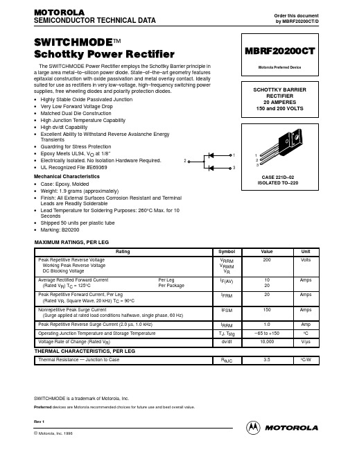
1
元器件交易网 MBRF20200CT
ELECTRICAL CHARACTERISTICS, PER LEG
Rating Maximum Instantaneous Forward Voltage (1) (iF = 10 Amp, TC = 25°C) (iF = 10 Amp, TC = 125°C) (iF = 20 Amp, TC = 25°C) (iF = 20 Amp, TC = 125°C) Maximum Instantaneous Reverse Current (1) (Rated dc Voltage, TC = 25°C) (Rated dc Voltage, TC = 125°C) Symbol vF 0.9 0.8 1.0 0.9 iR 1.0 50 mA Max Unit Volts
MBR30200CT-ASEMI

如何看产品参数?
【MBR30200CT】代表本产品的完 整型号 其中【MBR】为本产品的封装方式 【30】代表其正向电流为30A 【200】代表其反向耐压为200V 后缀【CT】代表芯片连接方式为 共阴连接
END 谢谢大家观看
如何看产品参数?
品牌:A。
DH18:生产批号
中 间 输 出
MBR30200CT 30电流参数:30A 200电压参数:200V CT:封装为TO-220共阴
MBR30200CT 外形尺寸参数
MBR30200CT产品解析
这款整流桥产品是采用了高纯度 无氧铜材料,导电性能更佳,引 脚加粗设计,宽度达1.01mm,可 持续长时间工作不发热。 产品表面采用激光打标,永不退 色,解决油墨丝印易掉色问题, 激光打标生产效率高,订货货期 短,解决油墨印字货期长、低效 率问题。
开 关 电 源 变频器
逆变器
MBR30200CT芯片工艺
这款肖特基产品是采用了俄罗斯Mikron芯片,高抗冲击性能 122MIL的芯片,品质稳定性与参数一致性非常好。 28条台湾健鼎测试线,确保MBR30200CT的高可靠性,确保产品 通过先进的生产工艺制作与严苛的电性监测,保障每一颗出厂 产品都能让客户放心。
MBR30200CT包装方式
它的包装方式为:一箱5000pcs,共5盒; 每盒1000pcs,共20管, 单管50pcs。
MBR30200CT 应用领域
MBR30200CT肖特基二极管广泛应用于开关电源、变频器、驱动 器等电路,作高频、低压、大电流整流二极管、续流二极管、 保护二极管使用,或在微波通信等电路中作整流二极管、小信 号检波二极管使用。
ASEMI课堂 产品介绍之MBR30200CT
MBR30200CT
MBR1545CT中文资料

Tj = 25°C f = 1 MHZ VSIG = 50mV p–p
1000
100 0.1
15344
1.0
10
100
VR – Reverse Voltage ( V )
Figure 4. Typ. Diode Capacitance vs. Reverse Voltage
Rev. A2, 24-Jun-98
15343
10
Tj = 150°C
1.0
Tj = 125°C
0.1
0.01
Tj = 75°C Tj = 25°C
10 Number of Cycles at 60 Hz
100
15345
0.001 0
20
40
60
80
100 120 140
Percent of Rated Peak Reverse Voltage (%)
Figure 3. Max. Peak Forward Surge Current vs. Number of Cycles
4000 C D – Diode Capacitance ( pF )
Figure 5. Typ. Reverse Current vs. Percent of Rated Peak Reverse Voltage
3 (5)
元器件交易网
MBR1530CT–MBR1560CT
Vishay Lite–On Power Semiconductor Dimensions in mm
14468
Case: molded plastic Polarity: as marked on body Approx. weight: 2.24 grams Mounting position: any Marking: type number
MBRB20100CTG中文资料
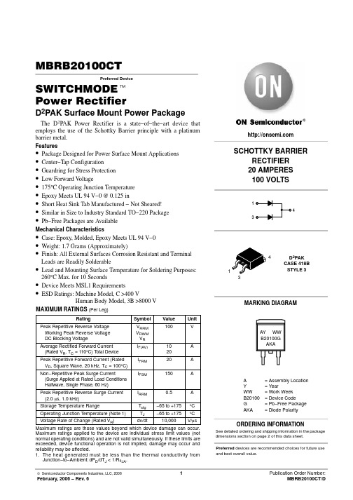
MBRB20100CTPreferred Device SWITCHMODE tPower RectifierD2PAK Surface Mount Power PackageThe D2PAK Power Rectifier is a state−of−the−art device that employs the use of the Schottky Barrier principle with a platinum barrier metal.Features•Package Designed for Power Surface Mount Applications •Center−T ap Configuration•Guardring for Stress Protection•Low Forward V oltage•175°C Operating Junction Temperature•Epoxy Meets UL 94 V−0 @ 0.125 in•Short Heat Sink Tab Manufactured − Not Sheared!•Similar in Size to Industry Standard TO−220 Package•Pb−Free Packages are AvailableMechanical Characteristics•Case: Epoxy, Molded, Epoxy Meets UL 94 V−0•Weight: 1.7 Grams (Approximately)•Finish: All External Surfaces Corrosion Resistant and Terminal Leads are Readily Solderable•Lead and Mounting Surface Temperature for Soldering Purposes: 260°C Max. for 10 Seconds•Device Meets MSL1 Requirements•ESD Ratings:Machine Model, C >400 VHuman Body Model, 3B >8000 VMAXIMUM RATINGS (Per Leg)Maximum ratings applied to the device are individual stress limit values (not normal operating conditions) and are not valid simultaneously. If these limits are exceeded, device functional operation is not implied, damage may occur and reliability may be affected.1.The heat generated must be less than the thermal conductivity fromJunction−to−Ambient: dP D/dT J < 1/R q JA.D2PAKCASE 418BSTYLE 3341SCHOTTKY BARRIERRECTIFIER20 AMPERES100 VOLTS13Preferred devices are recommended choices for future use and best overall value.MARKING DIAGRAMAY WWB20100GAKASee detailed ordering and shipping information in the package dimensions section on page 2 of this data sheet.ORDERING INFORMATIONA= Assembly LocationY= YearWW= Work WeekB20100= Device CodeG= Pb−Free PackageAKA= Diode PolarityELECTRICAL CHARACTERISTICS (Per Leg)3.Pulse Test: Pulse Width = 300 m s, Duty Cycle ≤2.0%.ORDERING INFORMATIONSpecifications Brochure, BRD8011/D.Figure 3. Typical Current Derating, Case, Per Leg i F , I N S T A N T A N E O U S F O R W A R D C U R R E N T (A M P S )AVERAGE CURRENT (AMPS)T C , CASE TEMPERATURE (°C)I F (A V ), A V E R A G E F O R W A R D C U R R E N T (A M P S )Figure 4. Average Power Dissipation & Average CurrentPACKAGE DIMENSIONSD 2PAK CASE 418B−04ISSUE Jǒmm inchesǓSOLDERING FOOTPRINT**For additional information on our Pb−Free strategy and solderingdetails, please download the ON Semiconductor Soldering and Mounting Techniques Reference Manual, SOLDERRM/D.STYLE 3:PIN 1.ANODE2.CATHODE3.ANODE4.CATHODEVARIABLEVIEW W−WVIEW W−WVIEW W−W123SWITCHMODE is a trademark of Semiconductor Components Industries, LLC.ON Semiconductor and are registered trademarks of Semiconductor Components Industries, LLC (SCILLC). SCILLC reserves the right to make changes without further notice to any products herein. SCILLC makes no warranty, representation or guarantee regarding the suitability of its products for any particular purpose, nor does SCILLC assume any liability arising out of the application or use of any product or circuit, and specifically disclaims any and all liability, including without limitation special, consequential or incidental damages.“Typical” parameters which may be provided in SCILLC data sheets and/or specifications can and do vary in different applications and actual performance may vary over time. All operating parameters, including “Typicals” must be validated for each customer application by customer’s technical experts. SCILLC does not convey any license under its patent rights nor the rights of others. SCILLC products are not designed, intended, or authorized for use as components in systems intended for surgical implant into the body, or other applications intended to support or sustain life, or for any other application in which the failure of the SCILLC product could create a situation where personal injury or death may occur. Should Buyer purchase or use SCILLC products for any such unintended or unauthorized application, Buyer shall indemnify and hold SCILLC and its officers, employees, subsidiaries, affiliates, and distributors harmless against all claims, costs, damages, and expenses, and reasonable attorney fees arising out of, directly or indirectly, any claim of personal injury or death associated with such unintended or unauthorized use, even if such claim alleges that SCILLC was negligent regarding the design or manufacture of the part. SCILLC is an Equal Opportunity/Affirmative Action Employer. This literature is subject to all applicable copyright laws and is not for resale in any manner.PUBLICATION ORDERING INFORMATION。
KOCH-MBR-技术手册
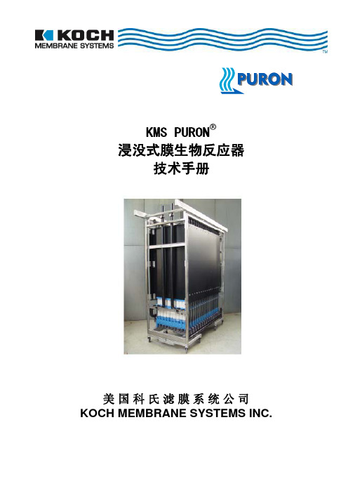
参数mbr传统工艺产水tssmg1015产水codmg304050沉淀后p总mg氧化池中的mlss含量kochchemicaltechnologygroupllccompany膜件特性参数特性参数性能指标技术类型超滤uf公称膜孔径005膜材料结构加筋pes膜丝内径外径12mm26mm过滤方向外进内出膜表面特性框架尺寸长宽高19819802800mm有效膜丝长度1800mm有效膜面积500m2产水母管直径dn80曝气管接口尺寸dn50膜件总重干400kg空气母管膜件排列空气分布管纤维护栏产水母管一端密封膜丝组件框架puronkochchemicaltechnologygroupllccompany表2500m2标准膜件运行参数特性参数指标ph适用范围312最高使用温度40运行压力05bar01bar反洗压力05bar三
厦门鲲扬膜科技有限公司MBR膜及产品介绍课件
进水浊度低于3NTU,通量50LMH 进水浊度1-3NTU,通量30LMH 用于料液过滤,前道工序需预处理(离心,砂滤,板框过滤等),通量5-12LMH
水洗 NaClO 1000-2000ppm 1小时 (废水) 膜清洗剂 (料液) 气洗
清洗条件
水洗 NaClO 1000-2000ppm 1小时 (废水) 膜清洗剂 (料液) 气洗
第二章.膜产品介绍
柱式膜——操作参数
4040 流量小于4m3/h,压力低于3Bar 温度低于50度 8050常温型 流量小于20m3/h ,压力低于3Bar 温度低于50度 8050高温型 流量小于20m3/h ,压力低于3Bar 温度低于80度
第二章.膜产品介绍
柱式膜——使用条件
使用条件和设计通量
西安建筑科技大学
上海问鼎环保
同济大学
闽南师范大学
浙江医药高专
2
公司B
废水
广州海纳
4
公司B
广州海纳
5
公司B
上海泰克比亚
1
公司B
广州海纳
6
公司B
韩国东国环境
1
公司B
山东大学环境系
2
科研
成都新塘环保
1
公司B
乌鲁木齐鸿安润诚
1
公司B
云南七冠科技
5
公司B
自来水
Metiska Farma
1
公司B
山东大学环境系
3
科研
陕西立佳工程
1
公司B
山东大学环境系
通化诺泽生物
1
公司A
中药分级过滤
厦门天泉鑫
1
公司B
玉米废水
华中师范大学化学学院
- 1、下载文档前请自行甄别文档内容的完整性,平台不提供额外的编辑、内容补充、找答案等附加服务。
- 2、"仅部分预览"的文档,不可在线预览部分如存在完整性等问题,可反馈申请退款(可完整预览的文档不适用该条件!)。
- 3、如文档侵犯您的权益,请联系客服反馈,我们会尽快为您处理(人工客服工作时间:9:00-18:30)。
NOTE
VF
.63 V .75 V .84 V
IR 8 mA TA = 25°C
∅ ∅ ∅
CJ
300pF
Measured at 1.0MHz, VR=4.0V
*Pulse Test: Pulse Width 300µsec, Duty Cycle 1%
元器件交易网
MCC
Figure 2 Forward Derating Curve
150
Single Phase, Half Wave 60Hz Resistive or Inductive Load 0 50 70 90 °C 110 130 150
Average Forward Rectified Current - Amperes versus Ambient Temperature - °C
元器件交易网
MCC
Features
• • • •ຫໍສະໝຸດ omponents 21201 Itasca Street Chatsworth !"# $
% !"#
Maximum Ratings
• • Operating Temperature: -65°C to +150°C Storage Temperature: -65°C to +150°C Maximum Recurrent Peak Reverse Voltage 20V 30V 35V 40V 45V 60V 80V 100V Maximum DC Blocking Voltage 20V 30V 35V 40V 45V 60V 80V 100V
A B K C M J F D H E L
G
Electrical Characteristics @ 25°C Unless Otherwise Specified
Average Forward Current Peak Forward Surge Current Maximum Instantaneous Forward Voltage 30020-30045CT 30060CT 30080-300100CT Maximum DC Reverse Current At Rated DC Blocking Voltage Typical Junction Capacitance IF(AV) IFSM 300 A 2500A TL = 140°C 8.3ms, half sine IFM = 150 A; TA = 25°C
MCC Part Number MBR30020CT MBR30030CT MBR30035CT MBR30040CT MBR30045CT MBR30060CT MBR30080CT MBR300100CT
Maximum RMS Voltage 14V 21V 24.5V 28V 31.5V 42V 56V 70V
MBR30020CT THRU MBR300100CT
300 Amp Schottky Barrier Rectifier 20 to 100 Volts FULL PACK
Metal of siliconrectifier, majonty carrier conducton Guard ring for transient protection Low power loss high efficiency High surge capacity, High current capability
元器件交易网
MBR30020CT thru MBR300100CT
Figure 4 Typical Reverse Characteristics 1000 600 400 2200 200 100 60 40 20 mAmps 8.0 4.0 3.0 2.0 1.0 .6 .4 .2 .1 10 20 TA=25°C 40 60 Volts Instantaneous Reverse Leakage Current - MicroAmperes versus Percent Of Rated Peak Reverse Voltage - Volts 80 100 120 TA=125°C 0 1 2 4 Amps 1900 1600 1000 500 2500
Figure 3 Junction Capacitance
1000 600 400 200 pF TJ=25°C 100 60 40 20 10 .1 .2 .4 1 Volts 2 4 10 20 40 100 200 400 1000
Junction Capacitance - pF versus Reverse Voltage - Volts
MCC
Figure 5 Peak Forward Surge Current
6
8 10 20 Cycles
40
60 80 100
Peak Forward Surge Current - Amperes versus Number Of Cycles At 60Hz - Cycles
MBR30020CT thru MBR300100CT
Figure 1 Typical Forward Characteristics 200 100 60 40 250 20 25°C Amps 10 6 4 2 1 .6 .4 .2 .1 0.6 0.8 1. 0 1.4 Volts Instantaneous Forward Current - Amperes versus Instantaneous Forward Voltage - Volts 1.8 2.0 0 50 Amps 100 200 300
DIM A B C E F G H J K L L DIMENSIONS INCH ES MIN MAX 3.150 NOM 1.565 1.585 .700 .800 .119 .132 1.375 REF 3.55 3.65 .590 .620 1/4 - UNF .380 .410 .185 .195 .275 .295 MM MIN MAX 80.01 NOM 39.75 40.26 17.78 20.32 3.02 3.35 34.92 REF 90.17 92.71 14.99 15.75 FULL 9.65 10.41 4.70 4.95 6.99 7.49
