MAX358CWE-T中文资料
MAX832中文资料
NUAL KIT MA ATION U EET L H A S V A E T WS DA FOLLO
___________________________Features
o Input Range: Up to 30V o 1A On-Chip Power Switch o Adjustable Output (MAX830) Fixed Outputs: 5V (MAX831) 3.3V (MAX832) 3V (MAX833) o 100kHz Switching Frequency o Excellent Dynamic Characteristics o Few External Components o 8mA Quiescent Current o 16-Pin SO Package o Evaluation Kit Available
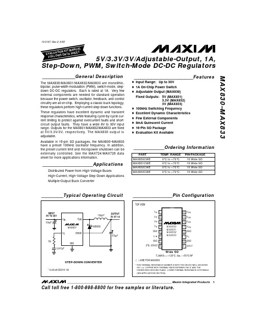
__________Typical Operating Circuit
__________________Pin Configuration
TOP VIEW
INPUT 8V TO 30V 100µF VIN VSW
100µH*
OUTPUT 5V AT 1A
V IN 1 V IN 2 V IN 3
16 V SW 15 V SW 14 V SW
_______________________Applications
Distributed Power from High-Voltage Buses High-Current, High-Voltage Step-Down Applications Multiple-Output Buck Converter
MAX831
VC 10k 0.047µF SENSE
MAX13085EESA-T中文资料

General DescriptionThe MAX13080E–MAX13089E +5.0V, ±15kV ESD-protect-ed, RS-485/RS-422 transceivers feature one driver and one receiver. These devices include fail-safe circuitry,guaranteeing a logic-high receiver output when receiver inputs are open or shorted. The receiver outputs a logic-high if all transmitters on a terminated bus are disabled (high impedance). The MAX13080E–MAX13089E include a hot-swap capability to eliminate false transitions on the bus during power-up or hot insertion.The MAX13080E/MAX13081E/MAX13082E feature reduced slew-rate drivers that minimize EMI and reduce reflections caused by improperly terminated cables, allowing error-free data transmission up to 250kbps. The MAX13083E/MAX13084E/MAX13085E also feature slew-rate-limited drivers but allow transmit speeds up to 500kbps. The MAX13086E/MAX13087E/MAX13088E driver slew rates are not limited, making transmit speeds up to 16Mbps possible. The MAX13089E slew rate is pin selectable for 250kbps,500kbps, and 16Mbps.The MAX13082E/MAX13085E/MAX13088E are intended for half-duplex communications, and the MAX13080E/MAX13081E/MAX13083E/MAX13084E/MAX13086E/MAX13087E are intended for full-duplex communica-tions. The MAX13089E is selectable for half-duplex or full-duplex operation. It also features independently programmable receiver and transmitter output phase through separate pins.The MAX13080E–MAX13089E transceivers draw 1.2mA of supply current when unloaded or when fully loaded with the drivers disabled. All devices have a 1/8-unit load receiver input impedance, allowing up to 256transceivers on the bus.The MAX13080E/MAX13083E/MAX13086E/MAX13089E are available in 14-pin PDIP and 14-pin SO packages.The MAX13081E/MAX13082E/MAX13084E/MAX13085E/MAX13087E/MAX13088E are available in 8-pin PDIP and 8-pin SO packages. The devices operate over the com-mercial, extended, and automotive temperature ranges.ApplicationsUtility Meters Lighting Systems Industrial Control Telecom Security Systems Instrumentation ProfibusFeatures♦+5.0V Operation♦Extended ESD Protection for RS-485/RS-422 I/O Pins±15kV Human Body Model ♦True Fail-Safe Receiver While Maintaining EIA/TIA-485 Compatibility ♦Hot-Swap Input Structures on DE and RE ♦Enhanced Slew-Rate Limiting Facilitates Error-Free Data Transmission(MAX13080E–MAX13085E/MAX13089E)♦Low-Current Shutdown Mode (Except MAX13081E/MAX13084E/MAX13087E)♦Pin-Selectable Full-/Half-Duplex Operation (MAX13089E)♦Phase Controls to Correct for Twisted-Pair Reversal (MAX13089E)♦Allow Up to 256 Transceivers on the Bus ♦Available in Industry-Standard 8-Pin SO PackageMAX13080E–MAX13089E+5.0V , ±15kV ESD-Protected, Fail-Safe, Hot-Swap, RS-485/RS-422 Transceivers________________________________________________________________Maxim Integrated Products 1Ordering Information19-3590; Rev 1; 4/05For pricing, delivery, and ordering information,please contact Maxim/Dallas Direct!at 1-888-629-4642, or visit Maxim’s website at .Selector Guide, Pin Configurations, and Typical Operating Circuits appear at end of data sheet.Ordering Information continued at end of data sheet.M A X 13080E –M A X 13089E+5.0V , ±15kV ESD-Protected, Fail-Safe, Hot-Swap, RS-485/RS-422 Transceivers 2_______________________________________________________________________________________ABSOLUTE MAXIMUM RATINGSDC ELECTRICAL CHARACTERISTICS(V CC = +5.0V ±10%, T A = T MIN to T MAX , unless otherwise noted. Typical values are at V CC = +5.0V and T A = +25°C.) (Note 1)Stresses beyond those listed under “Absolute Maximum Ratings” may cause permanent damage to the device. These are stress ratings only, and functional operation of the device at these or any other conditions beyond those indicated in the operational sections of the specifications is not implied. Exposure to absolute maximum rating conditions for extended periods may affect device reliability.(All Voltages Referenced to GND)Supply Voltage (V CC ).............................................................+6V Control Input Voltage (RE , DE, SLR,H/F , TXP, RXP)......................................................-0.3V to +6V Driver Input Voltage (DI)...........................................-0.3V to +6V Driver Output Voltage (Z, Y, A, B).............................-8V to +13V Receiver Input Voltage (A, B)....................................-8V to +13V Receiver Input VoltageFull Duplex (A, B)..................................................-8V to +13V Receiver Output Voltage (RO)....................-0.3V to (V CC + 0.3V)Driver Output Current.....................................................±250mAContinuous Power Dissipation (T A = +70°C)8-Pin SO (derate 5.88mW/°C above +70°C).................471mW 8-Pin Plastic DIP (derate 9.09mW/°C above +70°C).....727mW 14-Pin SO (derate 8.33mW/°C above +70°C)...............667mW 14-Pin Plastic DIP (derate 10.0mW/°C above +70°C)...800mW Operating Temperature RangesMAX1308_EC_ _.................................................0°C to +75°C MAX1308_EE_ _..............................................-40°C to +85°C MAX1308_EA_ _............................................-40°C to +125°C Junction Temperature......................................................+150°C Storage Temperature Range.............................-65°C to +150°C Lead Temperature (soldering, 10s).................................+300°CMAX13080E–MAX13089E+5.0V , ±15kV ESD-Protected, Fail-Safe, Hot-Swap, RS-485/RS-422 Transceivers_______________________________________________________________________________________3DC ELECTRICAL CHARACTERISTICS (continued)(V CC = +5.0V ±10%, T A = T MIN to T MAX , unless otherwise noted. Typical values are at V CC = +5.0V and T A = +25°C.) (Note 1)M A X 13080E –M A X 13089E+5.0V , ±15kV ESD-Protected, Fail-Safe, Hot-Swap, RS-485/RS-422 Transceivers 4_______________________________________________________________________________________DRIVER SWITCHING CHARACTERISTICSMAX13080E/MAX13081E/MAX13082E/MAX13089E WITH SRL = UNCONNECTED (250kbps)(V CC = +5.0V ±10%, T A = T MIN to T MAX , unless otherwise noted. Typical values are at V CC = +5.0V and T A = +25°C.)RECEIVER SWITCHING CHARACTERISTICSMAX13080E/MAX13081E/MAX13082E/MAX13089E WITH SRL = UNCONNECTED (250kbps)(V CC = +5.0V ±10%, T A = T MIN to T MAX , unless otherwise noted. Typical values are at V CC = +5.0V and T A = +25°C.)MAX13080E–MAX13089E+5.0V , ±15kV ESD-Protected, Fail-Safe, Hot-Swap, RS-485/RS-422 Transceivers_______________________________________________________________________________________5DRIVER SWITCHING CHARACTERISTICSMAX13083E/MAX13084E/MAX13085E/MAX13089E WITH SRL = V CC (500kbps)(V CC = +5.0V ±10%, T A = T MIN to T MAX , unless otherwise noted. Typical values are at V CC = +5.0V and T A = +25°C.)RECEIVER SWITCHING CHARACTERISTICSMAX13083E/MAX13084E/MAX13085E/MAX13089E WITH SRL = V CC (500kbps)(V CC = +5.0V ±10%, T A = T MIN to T MAX , unless otherwise noted. Typical values are at V CC = +5.0V and T A = +25°C.)M A X 13080E –M A X 13089E+5.0V , ±15kV ESD-Protected, Fail-Safe, Hot-Swap, RS-485/RS-422 Transceivers 6_______________________________________________________________________________________DRIVER SWITCHING CHARACTERISTICSMAX13086E/MAX13087E/MAX13088E/MAX13089E WITH SRL = GND (16Mbps)(V CC = +5.0V ±10%, T A = T MIN to T MAX , unless otherwise noted. Typical values are at V CC = +5.0V and T A = +25°C.)RECEIVER SWITCHING CHARACTERISTICSMAX13086E/MAX13087E/MAX13088E/MAX13089E WITH SRL = GND (16Mbps)(V CC = +5.0V ±10%, T A = T MIN to T MAX , unless otherwise noted. Typical values are at V CC = +5.0V and T A = +25°C.)Note 2:∆V OD and ∆V OC are the changes in V OD and V OC , respectively, when the DI input changes state.Note 3:The short-circuit output current applies to peak current just prior to foldback current limiting. The short-circuit foldback outputcurrent applies during current limiting to allow a recovery from bus contention.MAX13080E–MAX13089E+5.0V , ±15kV ESD-Protected, Fail-Safe, Hot-Swap, RS-485/RS-422 Transceivers_______________________________________________________________________________________70.800.901.501.101.001.201.301.401.60-40-10520-253550958011065125SUPPLY CURRENT vs. TEMPERATURETEMPERATURE (°C)S U P P L Y C U R R E N T (m A )0201040305060021345OUTPUT CURRENTvs. RECEIVER OUTPUT-HIGH VOLTAGEM A X 13080E -89E t o c 02OUTPUT HIGH VOLTAGE (V)O U T P U T C U R R E N T (m A )20104030605070021345OUTPUT CURRENTvs. RECEIVER OUTPUT-LOW VOLTAGEM A X 13080E -89E t o c 03OUTPUT LOW VOLTAGE (V)O U T P U T C U R R E N T (m A )4.04.44.24.84.65.25.05.4RECEIVER OUTPUT-HIGH VOLTAGEvs. TEMPERATURETEMPERATURE (°C)O U T P U T H I G H V O L T A G E (V )-40-10520-2535509580110651250.10.70.30.20.40.50.60.8RECEIVER OUTPUT-LOW VOLTAGEvs. TEMPERATURETEMPERATURE (°C)O U T P U T L O W V O L T A G E (V )-40-10520-25355095801106512502040608010012014016012345DRIVER DIFFERENTIAL OUTPUT CURRENT vs. DIFFERENTIAL OUTPUT VOLTAGEDIFFERENTIAL OUTPUT VOLTAGE (V)D I F FE R E N T I A L O U T P U T C U R R E N T (m A )2.02.82.43.63.24.44.04.8DRIVER DIFFERENTIAL OUTPUT VOLTAGE vs. TEMPERATURED I F FE R E N T I A L O U T P U T V O L T A G E (V )-40-10520-253550958011065125TEMPERATURE (°C)40201008060120140180160200-7-5-4-6-3-2-1012354OUTPUT CURRENT vs. TRANSMITTEROUTPUT-HIGH VOLTAGEOUTPUT HIGH VOLTAGE (V)O U T P U T C U R R E N T (m A )60402080100120140160180200042681012OUTPUT CURRENT vs. TRANSMITTEROUTPUT-LOW VOLTAGEOUTPUT-LOW VOLTAGE (V)O U T P U T C U R R E N T (m A )Typical Operating Characteristics(V CC = +5.0V, T A = +25°C, unless otherwise noted.)M A X 13080E –M A X 13089E+5.0V , ±15kV ESD-Protected, Fail-Safe, Hot-Swap, RS-485/RS-422 Transceivers 8_______________________________________________________________________________________21543679810SHUTDOWN CURRENT vs. TEMPERATUREM A X 13080E -89E t o c 10S H U T D O W N C U R R E N T (µA )-40-10520-253550958011065125TEMPERATURE (°C)600800700100090011001200DRIVER PROPAGATION DELAY vs. TEMPERATURE (250kbps)D R I VE R P R O P A G A T I O N D E L A Y (n s )-40-10520-253550958011065125TEMPERATURE (°C)300400350500450550600DRIVER PROPAGATION DELAY vs. TEMPERATURE (500kbps)D R I VE R P R O P A G A T I O N D E L A Y (n s )-40-10520-253550958011065125TEMPERATURE (°C)1070302040506080DRIVER PROPAGATION DELAY vs. TEMPERATURE (16Mbps)D R I VE R P R O P A G A T I O N D E L A Y (n s )-40-10520-253550958011065125TEMPERATURE (°C)40201008060120140160180RECEIVER PROPAGATION DELAYvs. TEMPERATURE (250kpbs AND 500kbps)R E C E I V E R P R O P A G A T I O N D E L A Y (n s )-40-10520-253550958011065125TEMPERATURE (°C)40201008060120140160180RECEIVER PROPAGATION DELAYvs. TEMPERATURE (16Mbps)R EC E I V E R P R O P A G AT I O N D E L A Y (n s )-40-10520-253550958011065125TEMPERATURE (°C)2µs/div DRIVER PROPAGATION DELAY (250kbps)DI 2V/divV Y - V Z 5V/divR L = 100Ω200ns/divRECEIVER PROPAGATION DELAY(250kbps AND 500kbps)V A - V B 5V/divRO 2V/divTypical Operating Characteristics (continued)(V CC = +5.0V, T A = +25°C, unless otherwise noted.)MAX13080E–MAX13089E+5.0V , ±15kV ESD-Protected, Fail-Safe, Hot-Swap, RS-485/RS-422 Transceivers_______________________________________________________________________________________9Test Circuits and Waveforms400ns/divDRIVER PROPAGATION DELAY (500kbps)DI 2V/divR L = 100ΩV Y - V Z 5V/div10ns/div DRIVER PROPAGATION DELAY (16Mbps)DI 2V/divR L = 100ΩV Y 2V/divV Z 2V/div40ns/divRECEIVER PROPAGATION DELAY (16Mbps)V B 2V/divR L = 100ΩRO 2V/divV A 2V/divTypical Operating Characteristics (continued)(V CC = +5.0V, T A = +25°C, unless otherwise noted.)Figure 2. Driver Timing Test CircuitM A X 13080E –M A X 13089E+5.0V , ±15kV ESD-Protected, Fail-Safe, Hot-Swap, RS-485/RS-422 Transceivers 10______________________________________________________________________________________Test Circuits and Waveforms (continued)Figure 4. Driver Enable and Disable Times (t DHZ , t DZH , t DZH(SHDN))DZL DLZ DLZ(SHDN)MAX13080E–MAX13089E+5.0V , ±15kV ESD-Protected, Fail-Safe, Hot-Swap, RS-485/RS-422 TransceiversTest Circuits and Waveforms (continued)Figure 6. Receiver Propagation Delay Test CircuitM A X 13080E –M A X 13089E+5.0V , ±15kV ESD-Protected, Fail-Safe, Hot-Swap, RS-485/RS-422 TransceiversMAX13080E–MAX13089E+5.0V , ±15kV ESD-Protected, Fail-Safe, Hot-Swap, RS-485/RS-422 TransceiversMAX13080E/MAX13083E/MAX13086EMAX13081E/MAX13084E/MAX13086E/MAX13087EFunction TablesM A X 13080E –M A X 13089E+5.0V , ±15kV ESD-Protected, Fail-Safe, Hot-Swap, RS-485/RS-422 Transceivers MAX13082E/MAX13085E/MAX13088EFunction Tables (continued)MAX13089EDetailed Description The MAX13080E–MAX13089E high-speed transceivers for RS-485/RS-422 communication contain one driver and one receiver. These devices feature fail-safe circuit-ry, which guarantees a logic-high receiver output when the receiver inputs are open or shorted, or when they are connected to a terminated transmission line with all dri-vers disabled (see the Fail-Safe section). The MAX13080E/MAX13082E/MAX13083E/MAX13085E/ MAX13086E/MAX13088E/MAX13089E also feature a hot-swap capability allowing line insertion without erroneous data transfer (see the Hot Swap Capability section). The MAX13080E/MAX13081E/MAX13082E feature reduced slew-rate drivers that minimize EMI and reduce reflec-tions caused by improperly terminated cables, allowing error-free data transmission up to 250kbps. The MAX13083E/MAX13084E/MAX13085E also offer slew-rate limits allowing transmit speeds up to 500kbps. The MAX13086E/MAX13087E/MAX13088Es’ driver slew rates are not limited, making transmit speeds up to 16Mbps possible. The MAX13089E’s slew rate is selectable between 250kbps, 500kbps, and 16Mbps by driving a selector pin with a three-state driver.The MAX13082E/MAX13085E/MAX13088E are half-duplex transceivers, while the MAX13080E/MAX13081E/ MAX13083E/MAX13084E/MAX13086E/MAX13087E are full-duplex transceivers. The MAX13089E is selectable between half- and full-duplex communication by driving a selector pin (H/F) high or low, respectively.All devices operate from a single +5.0V supply. Drivers are output short-circuit current limited. Thermal-shutdown circuitry protects drivers against excessive power dissi-pation. When activated, the thermal-shutdown circuitry places the driver outputs into a high-impedance state.Receiver Input Filtering The receivers of the MAX13080E–MAX13085E, and the MAX13089E when operating in 250kbps or 500kbps mode, incorporate input filtering in addition to input hysteresis. This filtering enhances noise immunity with differential signals that have very slow rise and fall times. Receiver propagation delay increases by 25% due to this filtering.Fail-Safe The MAX13080E family guarantees a logic-high receiver output when the receiver inputs are shorted or open, or when they are connected to a terminated transmission line with all drivers disabled. This is done by setting the receiver input threshold between -50mV and -200mV. If the differential receiver input voltage (A - B) is greater than or equal to -50mV, RO is logic-high. If (A - B) is less than or equal to -200mV, RO is logic-low. In the case of a terminated bus with all transmitters disabled, the receiv-er’s differential input voltage is pulled to 0V by the termi-nation. With the receiver thresholds of the MAX13080E family, this results in a logic-high with a 50mV minimumnoise margin. Unlike previous fail-safe devices, the-50mV to -200mV threshold complies with the ±200mVEIA/TIA-485 standard.Hot-Swap Capability (Except MAX13081E/MAX13084E/MAX13087E)Hot-Swap InputsWhen circuit boards are inserted into a hot or powered backplane, differential disturbances to the data buscan lead to data errors. Upon initial circuit board inser-tion, the data communication processor undergoes itsown power-up sequence. During this period, the processor’s logic-output drivers are high impedanceand are unable to drive the DE and RE inputs of these devices to a defined logic level. Leakage currents up to±10µA from the high-impedance state of the proces-sor’s logic drivers could cause standard CMOS enableinputs of a transceiver to drift to an incorrect logic level. Additionally, parasitic circuit board capacitance couldcause coupling of V CC or GND to the enable inputs. Without the hot-swap capability, these factors could improperly enable the transceiver’s driver or receiver.When V CC rises, an internal pulldown circuit holds DElow and RE high. After the initial power-up sequence,the pulldown circuit becomes transparent, resetting thehot-swap tolerable input.Hot-Swap Input CircuitryThe enable inputs feature hot-swap capability. At theinput there are two NMOS devices, M1 and M2 (Figure 9). When V CC ramps from zero, an internal 7µstimer turns on M2 and sets the SR latch, which alsoturns on M1. Transistors M2, a 1.5mA current sink, andM1, a 500µA current sink, pull DE to GND through a5kΩresistor. M2 is designed to pull DE to the disabledstate against an external parasitic capacitance up to100pF that can drive DE high. After 7µs, the timer deactivates M2 while M1 remains on, holding DE low against three-state leakages that can drive DE high. M1 remains on until an external source overcomes the required input current. At this time, the SR latch resetsand M1 turns off. When M1 turns off, DE reverts to a standard, high-impedance CMOS input. Whenever V CCdrops below 1V, the hot-swap input is reset.For RE there is a complementary circuit employing two PMOS devices pulling RE to V CC. MAX13080E–MAX13089E+5.0V, ±15kV ESD-Protected, Fail-Safe, Hot-Swap, RS-485/RS-422 TransceiversM A X 13080E –M A X 13089EMAX13089E ProgrammingThe MAX13089E has several programmable operating modes. Transmitter rise and fall times are programma-ble, resulting in maximum data rates of 250kbps,500kbps, and 16Mbps. To select the desired data rate,drive SRL to one of three possible states by using a three-state driver: V CC , GND, or unconnected. F or 250kbps operation, set the three-state device in high-impedance mode or leave SRL unconnected. F or 500kbps operation, drive SRL high or connect it to V CC .F or 16Mbps operation, drive SRL low or connect it to GND. SRL can be changed during operation without interrupting data communications.Occasionally, twisted-pair lines are connected backward from normal orientation. The MAX13089E has two pins that invert the phase of the driver and the receiver to cor-rect this problem. F or normal operation, drive TXP and RXP low, connect them to ground, or leave them uncon-nected (internal pulldown). To invert the driver phase,drive TXP high or connect it to V CC . To invert the receiver phase, drive RXP high or connect it to V CC . Note that the receiver threshold is positive when RXP is high.The MAX13089E can operate in full- or half-duplex mode. Drive H/F low, leave it unconnected (internal pulldown), or connect it to GND for full-duplex opera-tion. Drive H/F high for half-duplex operation. In full-duplex mode, the pin configuration of the driver and receiver is the same as that of a MAX13080E. In half-duplex mode, the receiver inputs are internally connect-ed to the driver outputs through a resistor-divider. This effectively changes the function of the device’s outputs.Y becomes the noninverting driver output and receiver input, Z becomes the inverting driver output and receiver input. In half-duplex mode, A and B are still connected to ground through an internal resistor-divider but they are not internally connected to the receiver.±15kV ESD ProtectionAs with all Maxim devices, ESD-protection structures are incorporated on all pins to protect against electro-static discharges encountered during handling and assembly. The driver outputs and receiver inputs of the MAX13080E family of devices have extra protection against static electricity. Maxim’s engineers have devel-oped state-of-the-art structures to protect these pins against ESD of ±15kV without damage. The ESD struc-tures withstand high ESD in all states: normal operation,shutdown, and powered down. After an ESD event, the MAX13080E–MAX13089E keep working without latchup or damage.ESD protection can be tested in various ways. The transmitter outputs and receiver inputs of the MAX13080E–MAX13089E are characterized for protec-tion to the following limits:•±15kV using the Human Body Model•±6kV using the Contact Discharge method specified in IEC 61000-4-2ESD Test ConditionsESD performance depends on a variety of conditions.Contact Maxim for a reliability report that documents test setup, test methodology, and test results.Human Body ModelFigure 10a shows the Human Body Model, and Figure 10b shows the current waveform it generates when dis-charged into a low impedance. This model consists of a 100pF capacitor charged to the ESD voltage of interest,which is then discharged into the test device through a 1.5k Ωresistor.IEC 61000-4-2The IEC 61000-4-2 standard covers ESD testing and performance of finished equipment. However, it does not specifically refer to integrated circuits. The MAX13080E family of devices helps you design equip-ment to meet IEC 61000-4-2, without the need for addi-tional ESD-protection components.+5.0V , ±15kV ESD-Protected, Fail-Safe, Hot-Swap, RS-485/RS-422 TransceiversThe major difference between tests done using the Human Body Model and IEC 61000-4-2 is higher peak current in IEC 61000-4-2 because series resistance is lower in the IEC 61000-4-2 model. Hence, the ESD with-stand voltage measured to IEC 61000-4-2 is generally lower than that measured using the Human Body Model. Figure 10c shows the IEC 61000-4-2 model, and Figure 10d shows the current waveform for IEC 61000-4-2 ESD Contact Discharge test.Machine Model The machine model for ESD tests all pins using a 200pF storage capacitor and zero discharge resis-tance. The objective is to emulate the stress caused when I/O pins are contacted by handling equipment during test and assembly. Of course, all pins require this protection, not just RS-485 inputs and outputs.Applications Information256 Transceivers on the BusThe standard RS-485 receiver input impedance is 12kΩ(1-unit load), and the standard driver can drive up to 32-unit loads. The MAX13080E family of transceivers has a1/8-unit load receiver input impedance (96kΩ), allowingup to 256 transceivers to be connected in parallel on one communication line. Any combination of these devices,as well as other RS-485 transceivers with a total of 32-unit loads or fewer, can be connected to the line.Reduced EMI and ReflectionsThe MAX13080E/MAX13081E/MAX13082E feature reduced slew-rate drivers that minimize EMI and reduce reflections caused by improperly terminated cables, allowing error-free data transmission up to250kbps. The MAX13083E/MAX13084E/MAX13085Eoffer higher driver output slew-rate limits, allowing transmit speeds up to 500kbps. The MAX13089E withSRL = V CC or unconnected are slew-rate limited. WithSRL unconnected, the MAX13089E error-free data transmission is up to 250kbps. With SRL connected toV CC,the data transmit speeds up to 500kbps. MAX13080E–MAX13089E+5.0V, ±15kV ESD-Protected, Fail-Safe, Hot-Swap, RS-485/RS-422 TransceiversM A X 13080E –M A X 13089ELow-Power Shutdown Mode (Except MAX13081E/MAX13084E/MAX13087E)Low-power shutdown mode is initiated by bringing both RE high and DE low. In shutdown, the devices typically draw only 2.8µA of supply current.RE and DE can be driven simultaneously; the devices are guaranteed not to enter shutdown if RE is high and DE is low for less than 50ns. If the inputs are in this state for at least 700ns, the devices are guaranteed to enter shutdown.Enable times t ZH and t ZL (see the Switching Characteristics section) assume the devices were not in a low-power shutdown state. Enable times t ZH(SHDN)and t ZL(SHDN)assume the devices were in shutdown state. It takes drivers and receivers longer to become enabled from low-power shutdown mode (t ZH(SHDN), t ZL(SHDN))than from driver/receiver-disable mode (t ZH , t ZL ).Driver Output ProtectionTwo mechanisms prevent excessive output current and power dissipation caused by faults or by bus contention.The first, a foldback current limit on the output stage,provides immediate protection against short circuits over the whole common-mode voltage range (see the Typical Operating Characteristics ). The second, a thermal-shut-down circuit, forces the driver outputs into a high-imped-ance state if the die temperature exceeds +175°C (typ).Line LengthThe RS-485/RS-422 standard covers line lengths up to 4000ft. F or line lengths greater than 4000ft, use the repeater application shown in Figure 11.Typical ApplicationsThe MAX13082E/MAX13085E/MAX13088E/MAX13089E transceivers are designed for bidirectional data commu-nications on multipoint bus transmission lines. F igures 12 and 13 show typical network applications circuits. To minimize reflections, terminate the line at both ends in its characteristic impedance, and keep stub lengths off the main line as short as possible. The slew-rate-lim-ited MAX13082E/MAX13085E and the two modes of the MAX13089E are more tolerant of imperfect termination.Chip InformationTRANSISTOR COUNT: 1228PROCESS: BiCMOS+5.0V , ±15kV ESD-Protected, Fail-Safe, Hot-Swap, RS-485/RS-422 TransceiversFigure 11. Line Repeater for MAX13080E/MAX13081E/MAX13083E/MAX13084E/MAX13086E/MAX13087E/MAX13089E in Full-Duplex Mode+5.0V, ±15kV ESD-Protected, Fail-Safe, Hot-Swap, RS-485/RS-422 TransceiversMAX13080E–MAX13089EM A X 13080E –M A X 13089E+5.0V , ±15kV ESD-Protected, Fail-Safe, Hot-Swap, RS-485/RS-422 TransceiversPin Configurations and Typical Operating CircuitsMAX13080E–MAX13089E+5.0V , ±15kV ESD-Protected, Fail-Safe, Hot-Swap, RS-485/RS-422 Transceivers______________________________________________________________________________________21Pin Configurations and Typical Operating Circuits (continued)M A X 13080E –M A X 13089E+5.0V , ±15kV ESD-Protected, Fail-Safe, Hot-Swap, RS-485/RS-422 Transceivers 22______________________________________________________________________________________Ordering Information (continued)MAX13080E–MAX13089E+5.0V , ±15kV ESD-Protected, Fail-Safe, Hot-Swap, RS-485/RS-422 Transceivers______________________________________________________________________________________23Package Information (continued)(The package drawing(s) in this data sheet may not reflect the most current specifications. For the latest package outline information,go to /packages .)。
TS358中文资料
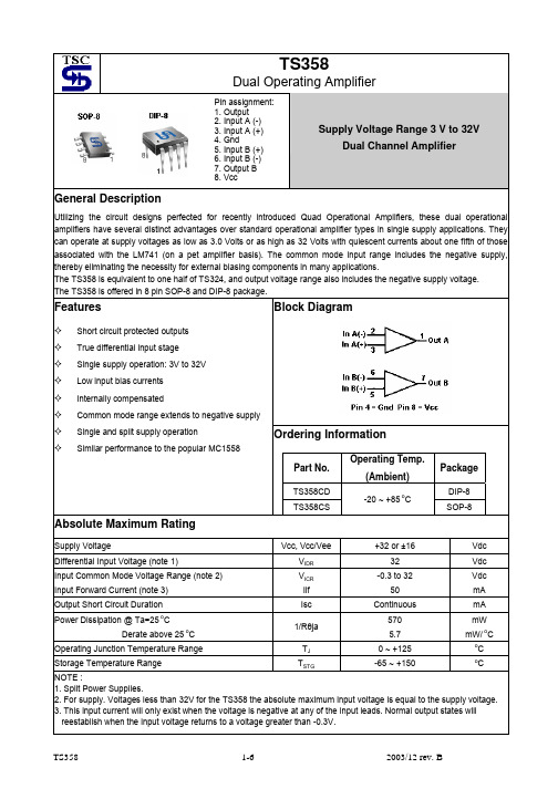
TS358Dual Operating AmplifierSupply Voltage Range 3 V to 32VDual Channel AmplifierGeneral DescriptionUtilizing the circuit designs perfected for recently introduced Quad Operational Amplifiers, these dual operational amplifiers have several distinct advantages over standard operational amplifier types in single supply applications. They can operate at supply voltages as low as 3.0 Volts or as high as 32 Volts with quiescent currents about one fifth of those associated with the LM741 (on a pet amplifier basis). The common mode input range includes the negative supply, thereby eliminating the necessity for external biasing components in many applications.The TS358 is equivalent to one half of TS324, and output voltage range also includes the negative supply voltage. The TS358 is offered in 8 pin SOP-8 and DIP-8 package.Block DiagramFeaturesShort circuit protected outputs True differential input stage Single supply operation: 3V to 32VLow input bias currentsInternally compensated Common mode range extends to negative supply Single and split supply operationSimilar performance to the popular MC1558Ordering InformationPart No.Operating Temp.(Ambient)PackageTS358CD DIP-8 TS358CS-20 ~ +85 oCSOP-8 Absolute Maximum RatingSupply VoltageVcc, Vcc/Vee+32 or ±16 Vdc Differential Input Voltage (note 1)V IDR 32 VdcInput Common Mode Voltage Range (note 2) Input Forward Current (note 3) V ICR Iif -0.3 to 3250 Vdc mA Output Short Circuit Duration Isc ContinuousmA Power Dissipation @ Ta=25 o CDerate above 25 oC1/R θja 570 5.7 mWmW/ oC Operating Junction Temperature Range T J 0 ~ +125 o C Storage Temperature RangeT STG-65 ~ +150oCNOTE :1. Split Power Supplies.2. For supply. Voltages less than 32V for the TS358 the absolute maximum input voltage is equal to the supply voltage.3. This input current will only exist when the voltage is negative at any of the input leads. Normal output states will reestablish when the input voltage returns to a voltage greater than -0.3V.Pin assignment:1. Output 2. Input A (-) 3. Input A (+) 4. Gnd5. Input B (+)6. Input B (-)7. Output B8. VccElectrical Characteristics(V CC = 5V, Ta=25 o C; unless otherwise specified.) Characteristics Symbol Min Typ Max UnitInput Offset VoltageV CC = 5.0V to 30V, V IC = 0V to Vcc -1.7 V, Vo= 1.4V, R S = 0Ω T LOW ≤ Ta ≤T HIGHVio-- -- 2.0 -- 5.0 7.0 mVAverage Temperature Coefficient of Input Offset Voltage Iio/T △△-- 7.0 -- uV/o CInput Offset Current T LOW ≤ Ta ≤T HIGHIio -- -- 5.0 -- 50 150 nAAverage Temperature Coefficient of input Offset Current Iio/T△△-- 10 -- pA/o CInput Bias Current T LOW ≤ Ta ≤T HIGHI IB-- 45 50 -250 -500 uAInput Common-Mode Voltage Range (Note1) V CC = 30 VV CC = 30 V, T LOW ≤ Ta ≤T HIGH V ICR 0 0 -- -- 28.3 28 V Differential Input Voltage Range V IDR -- -- V CC VLarge Signal Open-Loop Voltage Gain R L = 2.0K, V CC =15V, For Large V O Swing, T LOW ≤ Ta ≤T HIGH A VOL 25 15100 ---- --V/mV Channel Separation 1.0 KHz to 20KHz-- -- -120 -- dB Common Mode Rejection Ratio R S ≤ 10 k ΩCMRR 65 70 -- dB Power Supply Rejection Ratio PSRR 65 100 -- dB Output Voltage Range, RL = 2K Ω V OR 0 -- 3.3 VOutput Voltage -- High Limit V CC = 30 V, R L = 2 k Ω V CC = 30 V, R L = 10 k Ω V OH 26 27-- 28-- --VOutput Voltage -- Low Limit V CC = 5.0 V, R L = 10 k Ω V OL -- 5.0 20mVOutput Source Current V ID =+1.0V,V CC =15V I O+ 20 40 -- mAOutput Sink Current V ID = -1.0 V, V CC = 15 V V ID = -1.0 V, V O = 200 mVI O- 10 12 20 50 -- -- mA uAOutput Short Circuit to Ground (Note 2) I OS -- 40 60 mAPower Supply Current , V CC = 30 VV O = 0 V, R L = ∞V CC = 5.0 V, V O = 0 V, R L = ∞ I CC ---- 1.50.7 3.01.2 mA Notes :1. The input common mode voltage or either input signal voltage should not be allowed to go negative by more than 0.3 V. The upper end of the common mode voltage range is Vcc 17V, but either or both inputs can go to +32V.2. Short circuits from the output to Vcc can cause excessive heating and eventual destruction. Destructive dissipation can recruit from simultaneous shorts on all amplifiers.Circuit DescriptionThe TS358 made using two internally compensated, two-stage operational amplifiers. The first stage performs not only the first stage gain function but also performs the level shifting and transconductance reduction functions. By reducing the transconductance, a smaller compensation capacitor (only 5.0pF) can be employed, thus saving chip area. Another feature of this input stage is that the input common mode range can include the negative supply or ground, in single supply operation, without saturating either the input devices or the differential to single-ended converter. The second stage consists of a standard current source load amplifier stage.Each amplifier is biased from an internal-voltage regulator, and which has a low temperature coefficient thus giving each amplifier good temperature characteristics as well as excellent power supply rejection.Circuit DescriptionElectrical Characteristics Curve。
公司(普飞诺)新推IC及替换型号

SOP16封装,EC:0至70摄氏度/将TTL信号转为232信号,功耗 更低可以3.3V供电 特点:232通信距离为25M左右,485通信距离为1200M左右。外围电路简单。 四:应用范围
一:线性稳压IC可以应用于:电池供电玩具,工业控制器,仪器仪表,医疗设备,电脑,电话,路由 器,门禁,安防,家用电器控制板等。
PFN3232CSE PFN3232ESE PFN202CSE
SOP16封装,CSA:0至70摄氏度/TTL信号转为232信号,比232 功耗更低 SOP16封装,ESA:-40至+85摄氏度/TTL信号转为232信号,比 232功耗更低
CSA:0至70摄氏度/将TTL信号转为232信号,与232外围电容 不同 SOP16封装,ESA:-40至+85摄氏度/将TTL信号转为232信号, PFN202ESE 与232外围电容不同 SOP16封装,EE:-40至+85摄氏度/将TTL信号转为232信号, PFN202EESE 功耗更低可以3.3V供电 PFN202ECSE
规格 SOP8封装,CSA:0至70摄氏度/将TTL信号转为485信号 SOP8封装,ESA:-40至+85摄氏度/将TTL信号转为485信号 SOP16封装,CSA:0至70摄氏度/将TTL信号转为232信号 SOP16封装,ESA:-40至+85摄氏度/将TTL信号转为232信号
5: 6: 7: 8: 9: 10:
二:开关式降压IC 序号 型号 规格 1: P2575s-3.3 SOT263封装,固定输出+3.3V 2: P2575T-3.3 TO220封装,固定输出+3.3V 3: P2575S-5.0 SOT263封装,固定输出+5V 4: P2575T-5.0 TO220封装,固定输出+5V 5: P2575S-12 SOT263封装,固定输出+12V 6: P2575T-12 TO220封装,固定输出+12V 7: P2575S-ADJ SOT263封装,输出可调 8: P2575T-ADJ TO220封装,输出可调 9: P2576S-3.3 SOT263封装,固定输出+3.3V 10: P2576T-3.3 TO220封装,固定输出+3.3V 11: P2576S-5.0 SOT263封装,固定输出+5V 12: P2576T-5.O TO220封装,固定输出+5V 13: P2576S-12 SOT263封装,固定输出+12V 14: P2576T-12 TO220封装,固定输出+12V 15: P2576S-ADJ SOT263封装,输出可调 16: P2576T-ADJ TO220封装,输出可调 17: P2596S-3.3 SOT263封装,固定输出+3.3V 18: P2596T-3.3 TO220封装,固定输出+3.3V 19: P2596S-5.0 SOT263封装,固定输出+5V 20: P2596T-5.0 TO220封装,固定输出+5V 21: P2596S-12 SOT263封装,固定输出+12V 22: P2596T-12 TO220封装,固定输出+12V 23: P2596T-ADJ TO220封装,输出可调 24: P2596S-ADJ SOT263封装,输出可调 特点:开关式降压IC,转换效率高,2575输出1A,2576/2596系列最大可输出3A,如2575/2576尾缀带有 HV输入可高达DC60V。默认输入40V。2596与2576两点不同1:开关频率2596为150K,2576为52K。2:259 最大输入为40V。 三:通信IC 序号 型号 1: PFN485CSA 2: PFN485ESA 3: PFN232CSE 4: PFN2 LM2575T-3.3 LM2575S-5.0 LM2575T-5.0 LM2575S-12 LM2575T-12 LM2575S-ADJ LM2575T-ADJ LM2576S-3.3 LM2576T-3.3 LM2576S-5.0 LM2576T-5.O LM2576S-12 LM2576T-12 LM2576S-ADJ LM2576T-ADJ LM2596S-3.3 LM2596T-3.3 LM2596S-5.0 LM2596T-5.0 LM2596S-12 LM2596T-12 LM2596T-ADJ LM2596S-ADJ 出3A,如2575/2576尾缀带有 为150K,2576为52K。2:2596
max3485esa中文资料
General Description The MAX3483, MAX3485, MAX3486, MAX3488,MAX3490, and MAX3491 are 3.3V , low-power transceivers forRS-485 and RS-422 communication. Each part containsone driver and one receiver. The MAX3483 and MAX3488feature slew-rate-limited drivers that minimize EMI andreduce reflections caused by improperly terminatedcables, allowing error-free data transmission at data ratesup to 250kbps. The partially slew-rate-limited MAX3486transmits up to 2.5Mbps. The MAX3485, MAX3490, andMAX3491 transmit at up to 10Mbps.Drivers are short-circuit current-limited and are protectedagainst excessive power dissipation by thermal shutdowncircuitry that places the driver outputs into a high-imped-ance state. The receiver input has a fail-safe feature thatguarantees a logic-high output if both inputs are opencircuit.The MAX3488, MAX3490, and MAX3491 feature full-duplex communication, while the MAX3483, MAX3485, andMAX3486 are designed for half-duplex communication.Applications ●Low-Power RS-485/RS-422 Transceivers ●Telecommunications ●Transceivers for EMI-Sensitive Applications ●Industrial-Control Local Area NetworksFeatures●Operate from a Single 3.3V Supply—No Charge Pump!●Interoperable with +5V Logic ●8ns Max Skew (MAX3485/MAX3490/MAX3491)●Slew-Rate Limited for Errorless Data Transmission (MAX3483/MAX3488)●2nA Low-Current Shutdown Mode (MAX3483/MAX3485/MAX3486/MAX3491)●-7V to +12V Common-Mode Input Voltage Range ●Allows up to 32 Transceivers on the Bus ●Full-Duplex and Half-Duplex Versions Available ●Industry Standard 75176 Pinout (MAX3483/MAX3485/MAX3486)●Current-Limiting and Thermal Shutdown for Driver Overload Protection 19-0333; Rev 1; 5/19Ordering Information continued at end of data sheet.*Contact factory for for dice specifications.PARTTEMP . RANGE PIN-PACKAGE MAX3483CPA0°C to +70°C 8 Plastic DIP MAX3483CSA0°C to +70°C 8 SO MAX3483C/D0°C to +70°C Dice*MAX3483EPA-40°C to +85°C 8 Plastic DIP MAX3483ESA-40°C to +85°C 8 SO MAX3485CPA0°C to +70°C 8 Plastic DIP MAX3485CSA0°C to +70°C 8 SO MAX3485C/D0°C to +70°C Dice*MAX3485EPA-40°C to +85°C 8 Plastic DIP MAX3485ESA -40°C to +85°C 8 SO PARTNUMBERGUARANTEED DATA RATE (Mbps)SUPPLY VOLTAGE (V)HALF/FULL DUPLEX SLEW-RATE LIMITED DRIVER/RECEIVER ENABLE SHUTDOWN CURRENT (nA)PIN COUNT MAX34830.25 3.0 to 3.6Half Yes Yes 28MAX348510Half No No 28MAX34862.5Half Yes Yes 28MAX34880.25Half Yes Yes —8MAX349010Half No No —8MAX349110Half No Yes 214MAX3483/MAX3485/MAX3486/MAX3488/MAX3490/MAX3491Selection TableOrdering Information找电子元器件上宇航军工Figure 1. MAX3483/MAX3485/MAX3486 Pin Configuration and Typical Operating Circuit Figure 2. MAX3488/MAX3490 Pin Configuration and Typical Operating Circuit Figure 3. MAX3491 Pin Configuration and Typical Operating CircuitMAX3486/MAX3488/MAX3490/MAX3491True RS-485/RS-422 TransceiversFigure 22. MAX3488/MAX3490/MAX3491 Full-Duplex RS-485 NetworkFigure 23. Line Repeater for MAX3488/MAX3490/MAX3491MAX3486/MAX3488/MAX3490/MAX3491True RS-485/RS-422 Transceivers。
MAX31855汉语版
MAX31855冷端补偿热电偶至数字输出转换器概述MAX31855具有冷端补偿,将K、J、N、T或E型热电偶信号转换成数字量(如果使用S和R型热电偶,请联系工厂)。
器件输出14位带符号数据,通过SPI TM兼容接口、以只读格式输出。
转换器的温度分辨率为0.25℃,最高温度读数为+1800℃,最低温度读数为-270℃,对于K型热电偶,温度范围为-200℃至+700℃,保持±2℃精度。
对于整个量程范围的精度及其它类型的热电偶,请参考Thermal Characteristics规格。
特性∑ 冷端补偿∑ 14位、0.25℃分辨率∑ 提供K、J、N、T或E型热电偶器件版本(如果使用S和R型热电偶,请联系工厂)(见表1)∑ 简单的SPI兼容接口(只读)∑ 检测热电偶对GND或V CC短路∑ 检测热电偶开路定购信息在数据资料的最后给出。
应用工业电器设备HVAC汽车相关型号以及配合该器件使用的推荐产品,请参见:MAX31855.relatedSPI是Motorola, Inc.的商标有关价格,供货及订购信息,请联络Maxim销售中心:1888 629 4642,或是直接访问网址:MAX3855冷端补偿热电偶至数字输出转换器详细说明MAX31855为热电偶至数字输出转换器,内置14位模/数转换器(ADC)。
器件带有冷端补偿检测修正、数字控制器、SPI兼容接口,以及相关的控制逻辑,在温度控制器、过程控制或监测系统中设计用于配合外部微控制器(µC)工作。
提供多个版本的器件,每个版本针对特定的热电偶类型(K、J、N、T或E型,如果使用S和R型,请联系工厂)进行优化和调整。
热电偶类型以器件型号后缀表示(例如MAX31855K),型号选择请参见定购信息表。
温度转换器件包括信号调理硬件电路,将热电偶信号调整到与ADC输入通道相匹配的电压。
T+和T-输入连接到内部电路,可减小热电偶引线引入的噪声误差。
将热电偶电压转换为等效的温度值之前,需要补偿热电偶冷端(器件环境温度)与0℃实际参考值的差异。
max3485中文资料
MAX3483, MAX3485, MAX3486, MAX3488, MAX3490以及MAX3491是用于RS-485与RS-422通信的3.3V,低功耗收发器,每个器件中都具有一个驱动器和一个接收器。
MAX3483和MAX3488具有限摆率驱动器,可以减小EMI,并降低由不恰当的终端匹配电缆引起的反射,实现最高250kbps的无差错数据传输。
MAX3486的驱动器摆率部分受限,可以实现最高2.5Mbps的传输速率。
MAX3485,MAX3490和MAX3491则可以实现最高10Mbps 的传输速率。
驱动器具有短路电流限制,并可以通过热关断电路将驱动器输出置为高阻状态,防止过度的功率损耗。
接收器输入具有失效保护特性,当输入开路时,可以确保逻辑高电平输出。
使用MAX3488, MAX3490和MAX3491可以实现全双工通信,而MAX3483,MAX3485与MAX3486则为半双工应用设计。
这篇文章介绍的就是MAX34852 芯片介绍2.1 主要特点半双工速率:10Mbps限摆率:NO接收允许控制:YES 关断电流:2 nA引脚数:82.2 引脚配置根据上图、上表可知:DE和RO为使能管脚。
DE为低电平、RE为低电平时为接收;DE 为高电平、RE为高电平时为发送;RO和DI为数据管脚。
RO为接收,DI为发送;因此我们经常将DE和RE直接连接,用一个IO口控制(见3.2 电路实现)。
3.1 应用场景工业控制局域网集成服务数字网络低功耗RS-485/RS-422收发器(我做的几个项目都是该功能)分组交换技术电信用于EMI敏感应用的收发器3.2 电路实现485是2线式,两个485接口的设备相连通过A、B两根线即可(也就是至少2个485芯片),连接方式如下图所示:我们使用MAX3485一般是用下图电路:从上图中我们可以看到:RO直接和TTL电平的UART_RX(或模拟串口的RX)相连,DI直接和TTL电平的UART_TX(或模拟串口的TX)相连,R34为1K。
max3485中文资料

MAX3483,MAX3485,MAX3486,MAX3488,MAX3490以及MAX3491是用于RS-485与RS-422通信的3.3V,低功耗收发器,每个器件中都具有一个驱动器和一个接收器。
MAX3483和MAX3488具有限摆率驱动器,可以减小EMI,并降低由不恰当的终端匹配电缆引起的反射,实现最高250kbps的无差错数据传输。
MAX3486的驱动器摆率部分受限,可以实现最高2.5Mbps的传输速率。
MAX3485,MAX3490和MAX3491则可以实现最高10Mbps 的传输速率。
驱动器具有短路电流限制,并可以通过热关断电路将驱动器输出置为高阻状态,防止过度的功率损耗。
接收器输入具有失效保护特性,当输入开路时,可以确保逻辑高电平输出。
特性●半双工●速率:10Mbps●限摆率:NO●接收允许控制:YES●关断电流:2nA●引脚数:8参数暂无MAX3485的参数信息引脚图与功能MAX3485ESA品牌厂家:Maxim Integrated(美信),MAX3485ESA 渠道分销商:2家,现货库存数量:1542 PCS,MAX3485ESA价格参考:¥8.121元。
Maxim Integrated(美信)MAX3485ESA参数(SOIC 8Pin 3V 10Mbps,封装:SOIC),MAX3485ESA中文资料和引脚图及功能表说明书PDF下载(17页,409KB),您可以在MAX3485ESA接口芯片规格书Datesheet数据手册中,查到MAX3485ESA引脚图及功能的应用电路图电压和使用方法,MAX3485ESA典型电路教程。
MAX3485ESA可以用什么代替?代换型号如:MAX3485CSA+T、MAX3485CSA替代换,MAX3485ESA芯片系列中文手册中包含MAX3485ESA各引脚定义说明介绍及MAX3485ESA引脚功能图解,用户中文手册MAX3485ESA芯片手册PDF下载(17页,409KB)。