MC13144中文资料
MC2410 用户手册说明书

SinoMCU RF 2.4G射频传输专用芯片MC2410用户手册V1.0目录1产品概要 (3)2产品特性 (3)3模块框图 (4)4端口定义 (4)4.1引脚排列 (4)4.2端口说明 (5)5电气特性 (6)6典型应用 (8)7SPI接口 (9)7.1SPI默认格式 (9)7.2SPI时序要求 (10)8发送/接收流程 (11)8.1RF初始化 (11)8.2短包发送/接收流程 (11)8.3长包发送/接收流程 (12)8.4进入IDLE模式流程 (13)8.5进入SLEEP模式流程 (13)8.6SLEEP唤醒 (13)8.7扫描RSSI流程 (13)8.8250K传输数据率的附加流程 (13)9寄存器信息 (15)10数据包格式 (19)11电源要求 (19)12发射功率的调整 (20)13ESOP8封装功能说明 (20)13.1MCU通讯接口 (20)13.2射频性能 (20)14应用注意事项 (21)14.1IO电压 (21)14.2CE管脚 (21)14.3POR (21)14.4状态转换 (21)14.5同步字使用注意事项 (22)15封装尺寸 (23)15.1SOP16 (23)15.2ESOP8 (23)16修订记录 (24)1产品概要本产品是一款低成本,高集成度的2.4GHz的无线收发芯片,片上集成发射机、接收机、频率综合器和GFSK调制解调器,具有高灵敏度、低功耗以及抗干扰能力强的优点,可适用于无线遥控、无线键鼠、无线通讯以及工业控制等领域。
片上的发射接收FIFO寄存器可以和MCU进行通信,存储数据,然后以1Mbps或250Kbps数据率在空中传输。
内置了CRC、FEC、Auto ACK和自动重传机制,可以大大简化系统设计并优化性能。
同时外围电路简单,只需搭配MCU以及少数外围被动元件。
为了提高电池使用寿命,芯片在各个环节都降低功耗,芯片最低工作电压可以到1.9V,最低睡眠模式电流小于1μA。
奥的斯电梯最新调试资料
For personal use only in study and research;not for commercial use调试手册奥的斯电梯有限公司文件编号:OH-CONB863_SUR_ZH授权AUTH. CAL4804This work and the information it contains are the property of Xizi Otis Elevator Company (“XOEC”). It is delivered~others on the express condition that it will be used only for, or on behalf of, XOEC; that neither it nor the information it contains will be reported or disclosed, in whole or in part, without the prior written consent of XOEC, and that on demand it and any copies will be promptly returned~XOEC.目录1概述 .................................................................................................................... 错误!未定义书签。
2检修模式运行条件检查 .................................................................................... 错误!未定义书签。
3检修模式GECB上电检查............................................................................... 错误!未定义书签。
麦克维尔一拖多 分体式家用商用中央空调MCC-T

多联系统 一拖二、一拖三机组充分满足多居室的空调要 求,减少了室外机的数量,使安装位置选择更 便捷灵活,且不影响建筑物的整体外观。
风扇
按“风扇”键,风量按“自动→低风→中风→高 风”的顺序改变送风速度,在送风模式下无自动 风设置。
睡眠
来电自启(可选) 机组在运行过程中如遇停电,再次来电后机组会 自动恢复到停电前的状态(机组出厂时未设定 来电自启功能)。 夜间或白天休息时间使用睡眠功能,可以更好地适 应睡眠状态,提高睡眠质量,同时还节能省电。
MMC050LRC 14500 5000 4500 10.1
MMC060LC — 5040 —
MCC060T 14400
MMC060LRC 17300 5373 5390 12.3
W A
W A
16.8 — 50(15/30/70) 46/44/42 61 39 1900
8.2 — 1900 39
10.2 — 1900 39
RESIDENTIAL / COMMERCIAL AIR CONDITIONER
★ 实物可能与印刷资料有差别,购买时请参考实机。 ★ 所有资料经过仔细审核,如有任何印刷错漏,麦克维尔公司不承担因此产生的后果。 ★ 机型、参数、性能会因产品的改良有所改变,恕不另行通知。具体参数请以产品铭牌为准。
CH1111-3000-I
具备左、右两种接管方向的标准机组可选,极大方便了设计 与施工。
清新健康
有强力杀菌酶过滤网、紫外线杀菌灯、光触媒过滤网等装置 可供选配,净化空气,可有效杀死多种有害人体健康的广谱 有害菌和阳性菌。(若实现此种功能,机组需配备回风箱)
智能网络集中控制系统(选配),可通过集中控制器或电脑软 件,对最多1024台机组进行远程集中控制。
mc14504

NOTES:1.DIMENSIONING AND TOLERANCING PER ANSI Y14.5M, 1982.SOEIAJ–16F SUFFIXPLASTIC EIAJ SOIC PACKAGECASE 966–01ISSUE OON Semiconductor and are trademarks of Semiconductor Components Industries, LLC (SCILLC). SCILLC reserves the right to make changeswithout further notice to any products herein. SCILLC makes no warranty, representation or guarantee regarding the suitability of its products for any particular purpose, nor does SCILLC assume any liability arising out of the application or use of any product or circuit, and specifically disclaims any and all liability,including without limitation special, consequential or incidental damages. “Typical” parameters which may be provided in SCILLC data sheets and/or specifications can and do vary in different applications and actual performance may vary over time. All operating parameters, including “Typicals” must be validated for each customer application by customer’s technical experts. SCILLC does not convey any license under its patent rights nor the rights of others.SCILLC products are not designed, intended, or authorized for use as components in systems intended for surgical implant into the body, or other applications intended to support or sustain life, or for any other application in which the failure of the SCILLC product could create a situation where personal injury or death may occur. Should Buyer purchase or use SCILLC products for any such unintended or unauthorized application, Buyer shall indemnify and hold SCILLC and its officers, employees, subsidiaries, affiliates, and distributors harmless against all claims, costs, damages, and expenses, and reasonable attorney fees arising out of, directly or indirectly, any claim of personal injury or death associated with such unintended or unauthorized use, even if such claim alleges that SCILLC was negligent regarding the design or manufacture of the part. SCILLC is an Equal Opportunity/Affirmative Action Employer.PUBLICATION ORDERING INFORMATIONCENTRAL/SOUTH AMERICA:Spanish Phone :303–308–7143 (Mon–Fri 8:00am to 5:00pm MST)Email :ONlit–spanish@ ASIA/PACIFIC : LDC for ON Semiconductor – Asia SupportPhone :303–675–2121 (Tue–Fri 9:00am to 1:00pm, Hong Kong Time)Toll Free from Hong Kong & Singapore:001–800–4422–3781Email : ONlit–asia@JAPAN : ON Semiconductor, Japan Customer Focus Center4–32–1 Nishi–Gotanda, Shinagawa–ku, Tokyo, Japan 141–8549Phone : 81–3–5740–2745Email : r14525@。
MC1404基准电压
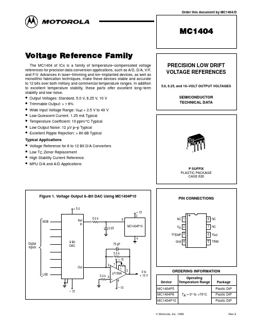
Gnd 4
ORDERING INFORMATION
Operating Temperature Range Package Plastic DIP TA = 0° to +70°C Plastic DIP Plastic DIP
+
MC1404P10
© Motorola, Inc. 1996
Rev 2
MOTOROLA ANALOG IC DEVICE DATA
Figure 3. Line Regulation versus Temperature
0
10
30 20 40 50 TA, AMBIENT TEMPERATURE (°C)
60
70
Figure 4. Output Voltage versus Temperature MC1404P10
0.010 10.04 Vout , OUTPUT VOLTAGE (V) LOAD REGULATION (%/mA) 10.02 10.00 9.98 9.96 9.94 0.008 0.006
SEMICONDUCTOR TECHNICAL DATA
Typical Applications
8 1
P SUFFIX PLASTIC PACKAGE CASE 626
Figure 1. Voltage Output 8–Bit DAC Using MC1404P10
+ 5.0 5.0 k 0.05 + 15 2 6 MC1404P10
40 35 30 25 20 15 10 5.0 0 0 10 20 30 40 50 TA, AMBIENT TEMPERATURE (°C) 60 70 Vin = 15 V V TEMP , TEMPERATURE OUTPUT (V) I sc , SHORT CIRCUIT CURRENT (mA) 1.0 0.8 0.6 0.4 IVTEMP = 10 nA 0.2 0
National Instruments SCXI-1314终端块安装指南说明书

National Instruments ™, ™, and SCXI ™ are trademarks of National Instruments Corporation. Product and company names mentioned herein are trademarks or trade names of their respective companies.322859A-01© Copyright 2000 National Instruments Corp. All rights reserved.August 2000SCXI -1314 U NIVERSAL S TRAIN T ERMINAL B LOCK This guide describes how to install and use the SCXI-1314 terminal block with your SCXI-1520 module.IntroductionThe SCXI-1314 terminal block is used with the SCXI-1520 universalstrain/bridge module enabling you to conveniently connect strain gauges through screw terminals. There are 88 screw terminals arranged in eight groups of 11. Each group corresponds to one of the eight channels available on the SCXI-1520. (Refer to Figure 2 for a diagram of terminal locations.) The signal names of the terminals for each channel are listed in Table 1.Each channel input contains screw terminals that connect to the inputs of the SCXI-1520, two precision 100 k Ω shunt calibration resistors, and a precision quarter-bridge completion resistor. The SCXI-1520 containsTable 1. Signal Names Signal NameCondition P+Positive excitation signal P–Negative excitation signal S+Positive input signal S–Negative input signal QTRQuarter-bridge completion resistor connection RS+Positive remote sense signal RS–Negative remote sense signal SCA(2 terminals)Shunt calibration A signal SCB(2 terminals)Shunt calibration B signal™relays that switch the resistors in and out of the input circuit to provideshunt calibration and quarter-bridge completion.The quarter-bridge completion resistor has a factory default value of 350Ωfor use with a 350Ω strain gauge. These resistors are placed in sockets onthe terminal block so you can easily replace them with resistors suitable toyour specific strain gauge. If your application requires a 120Ω straingauge, use the eight 120Ω resistors included in the kit.For a complete description of the use and operation of the SCXI-1520module, refer to the SCXI-1520 User Manual.What You Need to Get StartedTo install and use your SCXI-1314 terminal block, you need the followingitems:❑SCXI-1314 terminal block❑SCXI-1314 Universal Strain Terminal Block Installation Guide❑Eight precision 120 Ω resistors for use in quarter-bridge completioncircuits (if using 120 Ω strain gauges)❑SCXI chassis❑SCXI-1520 module❑SCXI-1520 User Manual❑Number 1 and 2 Phillips-head screwdrivers❑1/8 in. flathead screwdriver❑Long-nose pliers❑Wire cutter❑Wire insulation stripperSCXI-1314 Universal Strain Terminal © National Instruments Corporation 3SCXI-1314 Universal Strain Terminal BlockConnecting the SignalsTo connect the signal to the terminal block, perform the following steps, referring to Figures 1 and 2 as necessary:Figure 1. SCXI-1314 Parts Locator Diagram1.Unscrew the top cover screws and remove the top cover.2.Loosen the strain-relief screws and remove the strain-relief bar.3.Run the signal wires through the strain-relief opening. You can add insulation or padding if necessary.4.Prepare your signal wire by stripping the insulation no more than 7mm.5.Connect the signal wires to the screw terminals by inserting thestripped end of the wire fully into the terminal. No bare wire shouldextend past the screw terminal. Exposed wire increases the risk of ashort circuit that can cause circuit failure.When connecting your signals to the SCXI-1314, follow the labelingon the SCXI-1314, as indicated in Figure 2.1Top Cover Screws 2Top Cover 3Thumbscrew 4Mating Connector 5Strain-Relief Bar 6Strain-Relief Screws 7Safety-Ground LugFigure 2. SCXI-1314 Signal Connections6.Tighten the terminal screws to a torque of 5 to 7 in.-lb.7.Reinstall the strain-relief bar and tighten the strain-relief screws.8.Reinstall the top cover and tighten the top cover screws.9.Connect the terminal block to the module front connector as explainedin the Installing the Terminal Block section.SCXI-1314 Universal Strain Terminal Installing the Terminal BlockTo connect the terminal block to the SCXI module front connector, performthe following steps:1.Connect the module front connector to its mating connector on theterminal block.2.Tighten the top and bottom thumbscrews on the back of the terminalblock to hold it securely in place.Cleaning the Terminal BlockClean the terminal block by brushing off light dust with a soft, nonmetallicbrush. Remove other contaminants with deionized water and a stiffnonmetallic brush. The unit must be completely dry and free fromcontaminants before returning it to service.Calibrating the Terminal BlockFor information on calibrating the SCXI-1314 see the SCXI-1314Universal Strain Terminal Block Calibration Procedure located online at/calibration and follow the link for Manual CalibrationProcedures.SpecificationsAll specifications are typical at 25°C unless otherwise specified.ElectricalAccuracy of resistors120Ω completion resistor...............±0.1%350Ω completion resistor...............±0.1%100 kΩ shunt calibration resistor....±0.1%Temperature coefficient of resistors120Ω completion resistor...............±10 ppm/°C350Ω completion resistor...............±10 ppm/°C100 kΩ shunt calibration resistor....±10 ppm/°C© National Instruments Corporation5SCXI-1314 Universal Strain Terminal BlockMechanicalResistor socketsMating lead size...............................0.023 to 0.026 in.Mating lead length...........................0.110 to 0.175 in.Lead spacing....................................0.500 in.EnvironmentOperating temperature............................0to50°CStorage temperature................................–20to70°CRelative humidity...................................10to90%Indoor use onlySCXI-1314 Universal Strain Terminal 。
新版1314供电设计剖析

1、供电系统一、采区概况:1314工作面位于+450~+525m东一采区,工作面设计采用综采工艺,移动变电站和控制站放在材料道,距切眼约250m。
1314工作面两道660V电气设备,由+450m变电所一台KBSG-400/6型和+525移变一台KBSG-400/6型变压器供电,工作面1140V电气设备由控制站一台KBSGZY-1250/6型和KBSGZY-1250/6型移变及一台KBSGZY-630/6型移变供电,移变高压侧电源均来自+600m采区变电所。
2、电压等级:高压系统电压等级为6kV,工作面电气设备的电压等级为1140V,材料道及运输道电气设备电压等级为660V,1140V,照明信号电压为127V, 36V为控制电压。
3、供电系统:工作面照明采用DJC36/127L(B)型矿用防爆多功能支架灯,工作面安装间隔为15m,总数为10盏;通讯信号采用KTC2型控制设备,工作面安装间隔为15m,转载机头根据需要安装1只,总数为11台;照明信号的127V电源采用控制站的ZBZ-10.0/1140信号照明综保,其设计原则按照最大供电负荷计算。
(具体见:表1-1 设备负荷统计表;图2~3 供电系统图)表1-1 设备负荷统计表二、动力变压器的选择﹙按需用系数法计算变压器容量台数)1、工作面1140V系统:PMAX =315×2(工作面大溜子两台315kW电机同时起动)=630kW ,ΣPN =1540kWKX =0.4+0.6×630/1540=0.65 ,取KX = 0.6加权平均功率因数取COSΦPJ =0.7考虑具体负荷情况,选用一台KBSGZY-800/6和一台KBSGZY-1250/6型移变供电,负荷分配见供电系统图。
1#移变带:工作面煤机、转载机和破碎机,负荷为:ΣP1=720+55+90=865kW Sj= KX×ΣP1/ COSΦPJ =0.6×865/0.7=741.4kVA <1250(KVA)选用一台KBSGZY-1250 6/1.2型移动变电站满足设备负荷要求。
Minolta 相机产品价格清单说明书

1.00
Step down adaptor ring (55mm to 52mm)
2.00
Flashgun (Deluxe II) with/capacitor, case
10.95
Lens adaptor mount (Leica)
7.95
Lens adaptor mount (Exakta)
7.95
1104 1503 1211/1212 122111222
SR-T 101 w / MC Rokkor 58mm fl1.4, case SR-T 101 w / MC Rokkor 55mn-i fl1.7 , case SR-T 101, body only SR-ls w / MC Rokkor 55mm ~/ 1.7, accessory
MC Macro 50mm f/3.5, intermediate tube,
reversing ring, case
189.50
Short Mount 135mm f/4 (for use with
extension bellows only), w/case
39.50
1720 1741 1742 1706 1707 1708 1709 1710 1722 1770 1772 1774 1701 1702 1703 1704 1705 1711 1771 1773 1775 1731 1732 1751 1752 1761 1762 1780
3.00
Eyepiece correction lens #7V (-2.0 diopter)
3.00
Eyepiece correction lens #8V (-3.0 diopter)
MC1413P
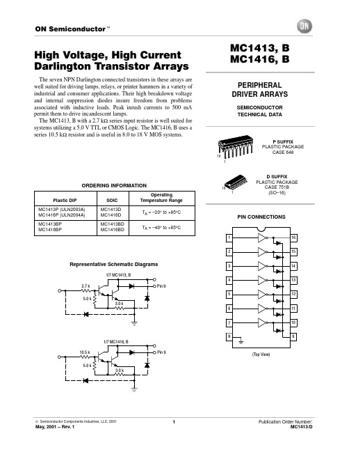
High Voltage, High Current Darlington Transistor ArraysThe seven NPN Darlington connected transistors in these arrays are well suited for driving lamps, relays, or printer hammers in a variety of industrial and consumer applications. Their high breakdown voltage and internal suppression diodes insure freedom from problems associated with inductive loads. Peak inrush currents to 500 mA permit them to drive incandescent lamps.The MC1413, B with a 2.7 k Ω series input resistor is well suited for systems utilizing a 5.0 V TTL or CMOS Logic. The MC1416, B uses a series 10.5 k Ω resistor and is useful in 8.0 to 18 V MOS systems.ORDERING INFORMATIONRepresentative Schematic DiagramsPin 9Pin 9MAXIMUM RATINGS (T= 25°C, and rating apply to any one device in the package, unless otherwise noted.)ELECTRICAL CHARACTERISTICS (T= 25°C, unless otherwise noted)% DUTY CYCLEV I , INPUT VOLTAGE (V)0100200400300500700600800I C , C O L L E C T O R C U R R E N T (m A )I I , I N P U T C U R R E N T (m A )N U M B E R O F D R I V E R S U S E D100400300200I I , INPUT CURRENT (µA)I O , O U T P U T C U R R E N T (m A )TYPICAL PERFORMANCE CURVES – T A = 25°CV I , INPUT VOLTAGE (V)I O , O U T P U T C U R R E N T (m A )Figure 1. Output Current versus Input VoltageFigure 2. Output Current versus Input CurrentFigure 5. Input Characteristics – MC1416, BFigure 6. Maximum Collector Currentversus Duty Cycle(and Number of Drivers in Use)NOTES:1.DIMENSIONING AND TOLERANCING PER ANSI Y14.5M, 1982.2.CONTROLLING DIMENSION: INCH.3.DIMENSION L TO CENTER OF LEADS WHEN FORMED PARALLEL.4.DIMENSION B DOES NOT INCLUDE MOLD FLASH.5.ROUNDED CORNERS OPTIONAL.MDIM MIN MAX MIN MAX MILLIMETERSINCHES A 0.7400.77018.8019.55B 0.2500.270 6.35 6.85C 0.1450.175 3.69 4.44D 0.0150.0210.390.53F 0.0400.70 1.02 1.77G 0.100 BSC 2.54 BSC H 0.050 BSC 1.27 BSC J 0.0080.0150.210.38K 0.1100.130 2.80 3.30L 0.2950.3057.507.74M 0 10 0 10 S0.0200.0400.51 1.01____P SUFFIXPLASTIC PACKAGE CASE 648–08ISSUE RNOTES:1.DIMENSIONING AND TOLERANCING PER ANSI Y14.5M, 1982.2.CONTROLLING DIMENSION: MILLIMETER.3.DIMENSIONS A AND B DO NOT INCLUDE MOLD PROTRUSION.4.MAXIMUM MOLD PROTRUSION 0.15 (0.006)PER SIDE.5.DIMENSION D DOES NOT INCLUDE DAMBAR PROTRUSION. ALLOWABLE DAMBARPROTRUSION SHALL BE 0.127 (0.005) TOTAL IN EXCESS OF THE D DIMENSION AT MAXIMUM MATERIAL CONDITION.SBM0.25 (0.010)AST DIM MIN MAX MIN MAX INCHESMILLIMETERS A 9.8010.000.3860.393B 3.80 4.000.1500.157C 1.35 1.750.0540.068D 0.350.490.0140.019F 0.40 1.250.0160.049G 1.27 BSC 0.050 BSC J 0.190.250.0080.009K 0.100.250.0040.009M 0 7 0 7 P 5.80 6.200.2290.244R0.250.500.0100.019____D SUFFIXPLASTIC PACKAGE CASE 751B–05(SO–16)ISSUE JON Semiconductor and are trademarks of Semiconductor Components Industries, LLC (SCILLC). SCILLC reserves the right to make changes without further notice to any products herein. SCILLC makes no warranty, representation or guarantee regarding the suitability of its products for any particular purpose, nor does SCILLC assume any liability arising out of the application or use of any product or circuit, and specifically disclaims any and all liability, including without limitation special, consequential or incidental damages. “Typical” parameters which may be provided in SCILLC data sheets and/or specifications can and do vary in different applications and actual performance may vary over time. All operating parameters, including “Typicals” must be validated for each customer application by customer’s technical experts. SCILLC does not convey any license under its patent rights nor the rights of others.SCILLC products are not designed, intended, or authorized for use as components in systems intended for surgical implant into the body, or other applications intended to support or sustain life, or for any other application in which the failure of the SCILLC product could create a situation where personal injury or death may occur. Should Buyer purchase or use SCILLC products for any such unintended or unauthorized application, Buyer shall indemnify and hold SCILLC and its officers, employees, subsidiaries, affiliates, and distributors harmless against all claims, costs, damages, and expenses, and reasonable attorney fees arising out of, directly or indirectly, any claim of personal injury or death associated with such unintended or unauthorized use, even if such claim alleges that SCILLC was negligent regarding the design or manufacture of the part. SCILLC is an Equal Opportunity/Affirmative Action Employer. PUBLICATION ORDERING INFORMATIONCENTRAL/SOUTH AMERICA:Spanish Phone:303–308–7143 (Mon–Fri 8:00am to 5:00pm MST)Email:ONlit–spanish@Toll–Free from Mexico: Dial 01–800–288–2872 for Access –then Dial 866–297–9322ASIA/PACIFIC: LDC for ON Semiconductor – Asia SupportPhone:1–303–675–2121 (Tue–Fri 9:00am to 1:00pm, Hong Kong Time)Toll Free from Hong Kong & Singapore:001–800–4422–3781Email: ONlit–asia@JAPAN: ON Semiconductor, Japan Customer Focus Center4–32–1 Nishi–Gotanda, Shinagawa–ku, Tokyo, Japan 141–0031Phone: 81–3–5740–2700。
中国五城市儿童掌指骨长度正常参考值

异常或综合征的相对骨节长度。 由表 2、表 3 也可见, 掌指 骨长 度增长 幅度 与掌
骨长度成比例, 即长度较长的掌骨和近节指骨长度 随年龄而增长的幅度较大, 而长度较短的中节指骨 和远节指骨长度增长的幅度较小, 因而在生长过程 中不同掌指骨之间的长度比例基本保持不变。 212 掌指骨长度 的变 异 儿 童掌 指骨 长度 的变 异 不尽相同, 按变异系数大小排序, 男女儿童中节指骨 5 、中节指骨 2 和近 节指 骨 1 的 相对 变异 程度 较 大, 而掌骨 2、掌骨 3、近节指骨 3、近节 指骨 4 相对 变异 较小( 表 5) ; 各排骨之间相比, 变异系数的大小排列 为远节指骨、中节指骨、近节指骨、掌骨; 如果在各排 骨内排序, 第 5 手 指各块 骨的相 对变异 程度 较大 ( 但男性掌骨排中掌骨 1 变异较大) 。
表 1 样本量的年龄组分布 ( 例)
性别 2 岁 3 岁 4 岁 5 岁 6 岁 7 岁 8 岁 9 岁 10 岁 11 岁 12 岁 13 岁 14 岁 15 岁 16 岁 17 岁 成 年
男
42
92 100 102 101 101 101 100 101 100 100 100 100 100 100 100 127
因此, 本文目的为制订中国五城市儿童掌指骨 长度正常值, 为临 床 遗 传 学和 内 分 泌 学 应用 MCPP 分析提供参考。 1 对象与方法 111 研究 对 象 研究 样 本 来 自《 中 国 人 手腕 骨 发 育标准—中 华 05 》[ 9] 中 的 上海 市、广 州市、温 州 市、 石家庄市、大连市五城市汉族正常儿童, 在 2 ~19 岁 各年龄组随机抽 取 100 例, 共 计 3 259 名 ( 男 1 667 名, 女1 592 名) , 见表 1。分别在 2 ~3 岁和 4 ~19 岁
RCC-M 晶间腐蚀和铁素体含量试验
MC1300 物理和物理化学试验MC1310 18—10型铬镍奥氏体不锈钢的加速晶间腐蚀试验MC1311 总则本试验的目的是检验产品是否具有良好的抗晶间腐蚀性能,足以承受其在加工和使用过程中的腐蚀条件。
根据如下加工方式和使用要求确定晶间腐蚀试验条件:——加工:热成型,焊接(各种方式);——使用:温度,环境。
下列方法适合于所有材料的各种严格的试验条件,和确定试验的严格程度。
MC1312 试验说明将特别制备并经晶间腐蚀敏化处理的试样浸泡在定量的试剂中并经过一段规定的时间。
该试剂为沸腾的硫酸铜硫酸溶液。
浸泡后用适当的方式评定试样是否发生了晶间腐蚀。
MC1312.1 取样按照附录SI中的技术规范和MC1315补充要求取样:——在收到的产品上取样;——或在加工的某些中间阶段取样。
——或在炼钢厂,在为取样而特别铸造的并经锻造成合适尺寸的样坯上取样。
注意:厚度过薄的试样(小于3mm),试验结果难以评定。
MC1312.2 试样的制备※试样应从试料上截取。
试样的取向,确切位置和尺寸均应按MC1315和如下规定执行:——从样坯上截取的试样,通常应是厚度3到4mm的,宽度为10mm左右,长度为60到70mm。
试样的轴线应平行于主锻造方向。
——板材或带材的试样应从产品本身上截取,加工到厚度为4mm并保留一个轧制面。
——管材试样可以从实际管道上截取。
当试验的目的是确定厚度小于3mm的不再进行热处理的板材或带材产品的可焊性时,其晶间腐蚀试验可以在按照MC1312.3的C法处理制备的焊接平板试样上进行。
MC1312.3 试验前试样的处理※※实际腐蚀试验前,试样应经下列一种“敏化”处理:——A法处理在实验室加热炉中,将试样加热至采购技术规范规定的温度“T”。
温度“T”:对不含钼的18—10型钢为650℃;对含钼的18—10型钢为675℃。
加热时间不超过5分钟,在温度偏差不超过±10℃下,保持10分钟。
然后,将试样浸入水中冷却。
mc1413中文资料

求输出控制隶属度
查表进行模糊推 理,获得模糊输出 输出量解模糊判 决,获得精确的压 缩机转速输出值
返回
PB PM
-6 0 0
-5 0 0
-4 0 0
-3 0 0
-2 0 0
-1 0 0
0 0 0
图5 压缩机转速控制子程序流程图 1 2 3 4 5 6 0 0 0 0.2 0.8 1 0 0.2 0.8 1 0.8 0.2
13
压缩机转速控制如上所述分为三个阶 PID 段开机设定阶段、 模糊逻辑控制阶段、 调节阶段。开机阶段根据系统运行状态确 定压缩机运行转速和持续时间,经过开机 阶段的设定运行判断是进入 PID 调节还是 进入模糊逻辑控制,由温差的大小决定。 当温差在 ± 1.5RC 以内时进入 PID 调节, 反 之进入模糊逻辑控制,如图 5 所示。根据 模糊控制系统的设计方法,首先确定制冷 控制系统的输入输出变量,以系统平均设 定温度与系统实际室内平均温度的偏差, 即系统平均设定温度偏差 ∆T 作为模糊控 制器的一个输入量,以系统平均设定温度 偏差 ∆T 的变化率 ∆T / ∆t 作为另一个输入 量,经过模糊控制器模糊化成为模糊矢量 E 和 EC。而以制冷系统的压缩机转速 Un 作为模糊控制器的输出变量。系统平均设 定温度偏差 ∆T 是指实测被控对象系统的 各室内环境温度值减去设定环境温度值的 差进行加权平均所得的值即为系统平均设 定温差 ∆T 。我们将系统平均设定温差 ∆T 控制范围分为模糊控制区和确定控制区, 以系统平均设定温差 ∆T 值的 ± 1.5R C 为 界。系统平均设定温差 ∆T 值在 ± 1.5 R C 以 外为模糊控制区,以内为确定控制区。在 开机工况完成后的 6 分钟时间内也为模糊 控制区,以利于系统迅速稳定。而在模糊 控制区,将系统平均设定温差 ∆T 分为 7 个模糊状态:PB(正的大 ∆T );PM(正的中 ∆T );PS(正的小 ∆T ) ;Z(正的零 ∆T ) ; NS(负的小 ∆T );NM(负的中 ∆T );NB(负 的大 ∆T )。将系统平均设定温差 ∆T 计算, 圆整, 并将范围大致划分为 13 个点, 分别 给出了它们对 7 个模糊状态的隶属度值, 即输入语言变量的取值:(负大、负中、负 小、零、正小、正中、正大)以符号{NB、 NM、NS、Z、PS、PM、PB}。语言值的 隶属函数选择三角形和梯形, 如表 1 所示。
视诚VSP 1314用户手册

11.RS232 控制接口 .................................................................................... 22
VSP 1314
用户手册
8
Hale Waihona Puke OUTPUT 输出接口................................................................................... 22 12.13.22.23: 千兆网接口.......................................................................... 22 14.24:发送卡电源接口 ........................................................................... 23 15.25:发送卡 USB 控制接口 .................................................................. 23 16.26:DVI 输入接口 ................................................................................ 23 20:DVI 输出接口 ..................................................................................... 23 21:DVI +VGA 的 DVI 输出接口................................................................ 23 开关及电源 ................................................................................................ 23 27.28:电源接口及开关 ........................................................................... 23
mc1413中文资料

ON Semiconductor MC14043B,MC14044B 数据手册

MC14043BTRUTH TABLEX = Don’t Care MC14044BS R E Q High ImpedanceX X 0No Change 011001101011111TRUTH TABLEX = Don’t CareS R E Q High ImpedanceX X 0010No Change01101011111ENABLER3S3R2S2R1S1R0S04367121114155Q3Q2Q1Q029101ENABLES3R3S2R2S1R1S0R04367121114155Q3Q2Q1Q0139101V DD = PIN 16V SS = PIN 8NC = PIN 2V DD = PIN 16V SS = PIN 8NC = PIN 13PIN ASSIGNMENT13141516910111254321876S2NC S3R3V DD Q1Q2R2S0R0Q0Q3V SSR1S1E 13141516910111254321876R2Q0R3S3V DD Q1Q2S2R0S0NC Q3V SSS1R1E NC = NO CONNECTIONMC14043BMC14044BELECTRICAL CHARACTERISTICS (Voltages Referenced to V SS )V – 55_C 25_C 125_CCharacteristicSymbol DD Vdc Min Max Min Typ (4.)Max Min Max Unit Output Voltage“0” LevelV in = V DD or 0V OL5.01015———0.050.050.05———0000.050.050.05———0.050.050.05Vdc“1” LevelV in = 0 or V DDV OH5.01015 4.959.9514.95———4.959.9514.955.01015———4.959.9514.95———VdcInput Voltage “0” Level(V O = 4.5 or 0.5 Vdc) (V O = 9.0 or 1.0 Vdc) (V O = 13.5 or 1.5 Vdc)V IL5.01015———1.53.04.0———2.254.506.75 1.53.04.0———1.53.04.0Vdc“1” Level(V O = 0.5 or 4.5 Vdc) (V O = 1.0 or 9.0 Vdc) (V O = 1.5 or 13.5 Vdc)V IH5.01015 3.57.011——— 3.57.0112.755.508.25——— 3.57.011———VdcOutput Drive Current(V OH = 2.5 Vdc) Source(V OH = 4.6 Vdc)(V OH = 9.5 Vdc)(V OH = 13.5 Vdc)I OH5.05.01015– 3.0– 0.64– 1.6– 4.2————– 2.4– 0.51– 1.3– 3.4– 4.2– 0.88– 2.25– 8.8————– 1.7– 0.36– 0.9– 2.4————mAdc(V OL = 0.4 Vdc) Sink(V OL = 0.5 Vdc)(V OL = 1.5 Vdc)I OL5.010150.641.64.2———0.511.33.40.882.258.8———0.360.92.4———mAdcInput Current I in 15—± 0.1—±0.00001± 0.1—± 1.0µAdc Input Capacitance(V in = 0)C in ———— 5.07.5——pF Quiescent Current(Per Package)I DD5.01015———1.02.04.0———0.0020.0040.0061.02.04.0———3060120µAdcTotal Supply Current (5.) (6.)(Dynamic plus Quiescent,Per Package)(C L = 50 pF on all outputs all buffers switching)I T5.01015I T = (0.58 µA/kHz) f + I DD I T = (1.15 µA/kHz) f + I DD I T = (1.73 µA/kHz) f + I DDµAdcThree–State Output Leakage CurrentI TL15—± 0.1—± 0.0001± 0.1—± 3.0µAdc4.Data labelled “Typ” is not to be used for design purposes but is intended as an indication of the IC’s potential performance.5.The formulas given are for the typical characteristics only at 25_C.6.To calculate total supply current at loads other than 50 pF:I T (C L ) = I T (50 pF) + (C L – 50) Vfkwhere: I T is in µA (per package), C L in pF, V = (V DD – V SS ) in volts, f in kHz is input frequency, and k = 0.004.SWITCHING CHARACTERISTICS (7.) (C L = 50 pF, T A = 25_C)CharacteristicSymbol V DDVdc Min Typ (8.)Max Unit Output Rise Timet TLH = (1.35 ns/pF) C L + 32.5 ns t TLH = (0.60 ns/pF) C L + 20 ns t TLH = (0.40 ns/pF) C L + 20 ns t TLH5.01015———100504020010080nsOutput Fall Timet THL = (1.35 ns/pF) C L + 32.5 ns t THL = (0.60 ns/pF) C L + 20 ns t THL = (0.40 ns/pF) C L + 20 ns t THL5.01015———100504020010080nsPropagation Delay Timet PLH = (0.90 ns/pF) C L + 130 ns t PLH = (0.36 ns/pF) C L + 57 ns t PLH = (0.26 ns/pF) C L + 47 ns t PLH5.01015———1757560350175120nst PHL = (0.90 ns/pF) C L + 130 ns t PHL = (0.90 ns/pF) C L + 57 ns t PHL = (0.26 ns/pF) C L + 47 nst PHL5.01015———1757560350175120nsSet, Set Pulse Widtht W5.0101520010070804030———nsReset, Reset Pulse Widtht W5.0101520010070804030———nsThree–State Enable/Disable Delayt PLZ ,t PHZ ,t PZL ,t PZH5.01015———1508055300160110ns7.The formulas given are for the typical characteristics only at 25_C.8.Data labelled “Typ” is not to be used for design purposes but is intended as an indication of the IC’s potential performance.AC WAVEFORMSMC14043BMC14044B20 ns20 ns90%10%RESETSETQt PHLt PLH20 ns20 ns50%90%50%10%t THLt TLH 90%50%10%V DD V SSV DD V SS V OH V OLRESETSETQ20 ns20 ns 90%10%50%20 ns20 ns 90%10%50%t TLHt THL50%10%90%t PLHt PHLV DD V SSV DD V SS V OH V OLTHREE–STATE ENABLE/DISABLE DELAYS Set, Reset, Enable, and Switch Conditions for 3–State TestsMC14043B MC14044B Test Enable S1S2Q S R S Rt PZH Open Closed A V DD V SS V SS V DDt PZL Closed Open B V SS V DD V DD V SSt PHZ Open Closed A V DD V SS V SS V DDt PLZ Closed Open B V SS V DD V DD V SSENABLEQ AQ B 50%t PZH10%t PZLt PHZt PLZ10%90%V DDV SSV DDV OLV OHV SSTOOUTPUTUNDERTESTV DDS1S21 kC L50 pFV SSPDIP–16P SUFFIXPLASTIC DIP PACKAGECASE 648–08ISSUE RNOTES:1.DIMENSIONING AND TOLERANCING PER ANSI Y14.5M, 1982.2.CONTROLLING DIMENSION: INCH.3.DIMENSION L TO CENTER OF LEADS WHEN FORMED PARALLEL.4.DIMENSION B DOES NOT INCLUDE MOLD FLASH.5.ROUNDED CORNERS OPTIONAL.–A–BFC SHGDJLM16 PLSEATING18916KPLANE–T–MAM0.25 (0.010)T DIM MIN MAX MIN MAX MILLIMETERS INCHES A 0.7400.77018.8019.55B 0.2500.270 6.35 6.85C 0.1450.175 3.69 4.44D 0.0150.0210.390.53F 0.0400.70 1.02 1.77G 0.100 BSC 2.54 BSC H 0.050 BSC 1.27 BSC J 0.0080.0150.210.38K 0.1100.130 2.80 3.30L 0.2950.3057.507.74M 0 10 0 10 S0.0200.0400.51 1.01____SOIC–16D SUFFIXPLASTIC SOIC PACKAGECASE 751B–05ISSUE JNOTES:1.DIMENSIONING AND TOLERANCING PER ANSI Y14.5M, 1982.2.CONTROLLING DIMENSION: MILLIMETER.3.DIMENSIONS A AND B DO NOT INCLUDE MOLD PROTRUSION.4.MAXIMUM MOLD PROTRUSION 0.15 (0.006)PER SIDE.5.DIMENSION D DOES NOT INCLUDE DAMBAR PROTRUSION. ALLOWABLE DAMBARPROTRUSION SHALL BE 0.127 (0.005) TOTAL IN EXCESS OF THE D DIMENSION AT MAXIMUM MATERIAL CONDITION.18169SEATINGPLANEFJMRX 45_G8 PLP–B––A–M0.25 (0.010)BS–T–DKC16 PLSBM0.25 (0.010)AST DIM MIN MAX MIN MAX INCHES MILLIMETERS A 9.8010.000.3860.393B 3.80 4.000.1500.157C 1.35 1.750.0540.068D 0.350.490.0140.019F 0.40 1.250.0160.049G 1.27 BSC 0.050 BSC J 0.190.250.0080.009K 0.100.250.0040.009M 0 7 0 7 P 5.80 6.200.2290.244R0.250.500.0100.019____H EA 1DIM MIN MAX MIN MAX INCHES––– 2.05–––0.081MILLIMETERS 0.050.200.0020.0080.350.500.0140.0200.180.270.0070.0119.9010.500.3900.4135.10 5.450.2010.2151.27 BSC 0.050 BSC 7.408.200.2910.3230.500.850.0200.0331.10 1.500.0430.0590 0.700.900.0280.035–––0.78–––0.031A 1H E Q 1L E _10 _0 _10 _L EQ 1_NOTES:1.DIMENSIONING AND TOLERANCING PER ANSI Y14.5M, 1982.2.CONTROLLING DIMENSION: MILLIMETER.3.DIMENSIONS D AND E DO NOT INCLUDE MOLD FLASH OR PROTRUSIONS AND AREMEASURED AT THE PARTING LINE. MOLD FLASH OR PROTRUSIONS SHALL NOT EXCEED 0.15(0.006) PER SIDE.4.TERMINAL NUMBERS ARE SHOWN FOR REFERENCE ONLY.5.THE LEAD WIDTH DIMENSION (b) DOES NOT INCLUDE DAMBAR PROTRUSION. ALLOWABLE DAMBAR PROTRUSION SHALL BE 0.08 (0.003)TOTAL IN EXCESS OF THE LEAD WIDTHDIMENSION AT MAXIMUM MATERIAL CONDITION.DAMBAR CANNOT BE LOCATED ON THE LOWER RADIUS OR THE FOOT. MINIMUM SPACEBETWEEN PROTRUSIONS AND ADJACENT LEAD TO BE 0.46 ( 0.018).M LDETAIL PVIEW PcAb eM0.13 (0.005)0.10 (0.004)11698DZE A b c D E e L M ZSOEIAJ–16F SUFFIXPLASTIC EIAJ SOIC PACKAGECASE 966–01ISSUE OON Semiconductor and are trademarks of Semiconductor Components Industries, LLC (SCILLC). SCILLC reserves the right to make changes without further notice to any products herein. SCILLC makes no warranty, representation or guarantee regarding the suitability of its products for any particular purpose, nor does SCILLC assume any liability arising out of the application or use of any product or circuit, and specifically disclaims any and all liability, including without limitation special, consequential or incidental damages. “Typical” parameters which may be provided in SCILLC data sheets and/or specifications can and do vary in different applications and actual performance may vary over time. All operating parameters, including “Typicals” must be validated for each customer application by customer’s technical experts. SCILLC does not convey any license under its patent rights nor the rights of others.SCILLC products are not designed, intended, or authorized for use as components in systems intended for surgical implant into the body, or other applications intended to support or sustain life, or for any other application in which the failure of the SCILLC product could create a situation where personal injury or death may occur. Should Buyer purchase or use SCILLC products for any such unintended or unauthorized application, Buyer shall indemnify and hold SCILLC and its officers, employees, subsidiaries, affiliates, and distributors harmless against all claims, costs, damages, and expenses, and reasonable attorney fees arising out of, directly or indirectly, any claim of personal injury or death associated with such unintended or unauthorized use, even if such claim alleges that SCILLC was negligent regarding the design or manufacture of the part. SCILLC is an Equal Opportunity/Affirmative Action Employer. PUBLICATION ORDERING INFORMATIONCENTRAL/SOUTH AMERICA:Spanish Phone:303–308–7143 (Mon–Fri 8:00am to 5:00pm MST)Email:ONlit–*********************ASIA/PACIFIC: LDC for ON Semiconductor – Asia SupportPhone:303–675–2121 (Tue–Fri 9:00am to 1:00pm, Hong Kong Time)Toll Free from Hong Kong & Singapore:001–800–4422–3781Email:ONlit–******************JAPAN: ON Semiconductor, Japan Customer Focus Center4–32–1 Nishi–Gotanda, Shinagawa–ku, Tokyo, Japan 141–8549Phone: 81–3–5740–2745Email:*****************。
MC14433电压表

MC1413的应用:(MC14433、CD4511、MC1413、MC1403组成的应用数字电压表)数字显示电压表将被测模拟量转换为数字量,并进行实时数字显示。
该系统(如图1 所示)可采用MC14433—三位半A/D 转换器、MC1413七路达林顿驱动器阵列、CD4511 BCD到七段锁存-译码-驱动器、能隙基准电源MC1403和共阴极LED发光数码管组成。
本系统是三位半数字电压表,三位半是指十进制数0000~1999。
所谓3位是指个位、十位、百位,其数字范围均为0~9,而所谓半位是指千位数,它不能从0变化到9,而只能由0变到l,即二值状态,所以称为半位。
各部分的功能如下:三位半A/D转换器(MC14433):将输入的模拟信号转换成数字信号。
基准电源(MC1403):提供精密电压,供A/D 转换器作参考电压。
译码器(MC4511):将二—十进制(BCD)码转换成七段信号。
驱动器(MC1413):驱动显示器的a,b,c,d,e,f,g七个发光段,驱动发光数码管(LED)进行显示。
显示器:将译码器输出的七段信号进行数字显示,读出A/D转换结果。
工作过程如下:三位半数字电压表通过位选信号DS1~DS4进行动态扫描显示,由于MC14433电路的A/D转换结果是采用BCD码多路调制方法输出,只要配上一块译码器,就可以将转换结果以数字方式实现四位数字的LED 发光数码管动态扫描显示。
DS1~DS4输出多路调制选通脉冲信号。
DS选通脉冲为高电平时表示对应的数位被选通,此时该位数据在Q0~Q3端输出。
每个DS选通脉冲高电平宽度为18个时钟脉冲周期,两个相邻选通脉冲之间间隔2个时钟脉冲周期。
DS和EOC的时序关系是在EOC 脉冲结束后,紧接着是DS1输出正脉冲。
以下依次为DS2,DS3和DS4。
其中DS1对应最高位(MSD),DS4则对应最低位(LSD)。
在对应DS2,DS3和DS4选通期间,Q0~Q3输出BCD全位数据,即以8421码方式输出对应的数字0~9.在DS1选通期间,Q0~Q3输出千位的半位数0或l及过量程、欠量程和极性标志信号。
- 1、下载文档前请自行甄别文档内容的完整性,平台不提供额外的编辑、内容补充、找答案等附加服务。
- 2、"仅部分预览"的文档,不可在线预览部分如存在完整性等问题,可反馈申请退款(可完整预览的文档不适用该条件!)。
- 3、如文档侵犯您的权益,请联系客服反馈,我们会尽快为您处理(人工客服工作时间:9:00-18:30)。
元器件交易网
A SOLUTION FOR THESE QUESTIONS (CONTINUED)
TYPES OF APPLICATIONS
• Any 900 MHz ISM band applications such as: Active RF tags Video or data link security systems Consumer or industrial remote control Remote keyless entry TV video links High fidelity audio links 2
• • •
A SOLUTION FOR THESE QUESTIONS
• • • Are you designing a wireless communications system that operates in the 900 MHz ISM or 1.8 to 2.0 GHz frequency range? Is reduced space or small printed circuit board size a critical design requirement? Do you want to reduce your system cost with a more cost-effective design requiring fewer external components? 3
BENБайду номын сангаасFITS TO YOU
• • • • • • Lowers system cost and manufacturing costs by reducing component count and circuit complexity over other solutions. Can be used in two-cell battery-powered applications with a power supply voltage as low as 1.8 V (MC13143/144). Improved battery life due to low power consumption, and standby mode when receiver is not in use. Provides system design flexibility with one-chip (MC13142) or two-chip (MC13143/144) RF front end solutions. Higher circuit and system density with small surface mount packages. Flexibility in receiver system partitioning because the differential open collector mixer outputs of the MC13142 and MC13143 simplify the interface to filters and back-end IF devices, such as the MC13158. Improved reliability due to lower power dissipation. Smaller battery for portable applications with 1.8 to 2.7 V operation. Optimized mixer loading for improved linearity with single-ended 50Ω double balanced mixer design.
- Wireless telephone headsets
元器件交易网
TYPES OF APPLICATIONS (CONTINUED)
• • • • • • • UHF Family Radio Services UHF and 800 MHz Special Mobile Radio 800 MHz cellular phones GSM, PCS, DECT and PHS handsets at 1.8 to 2.0 GHz Cordless phones in the 902 to 928 MHz band High power spread spectrum and low power data links in the 900 MHz ISM band Wideband data links
Can also contribute to extended battery life This new family of RF building blocks consists of the MC13142, MC13143 and MC13144. All three ICs are designed using Motorola’s MOSAIC VTM high frequency bipolar wafer process to provide excellent performance in both analog and digital communication systems. The MC13142 provides a general purpose solution for RF front ends because it contains all of the basic functions needed. The MC13143 and MC13144 combine to provide a higher performance solution for RF front ends. The system partitioning between the MC13143 and 13144 provides improved isolation, more versatility, and simplifies the interface with external devices such as filters and other active components. The MC13143 is a high compression linear mixer with a single-ended RF input, differential IF output, and differential local oscillator (LO) inputs, which consumes as little as 1.8 mW. This mixer is designed for up or down conversion anywhere from DC to 2.4 GHz. The MC13144 is a low noise amplifier (LNA) with programmable bias. The device includes a cascode LNA that is usable at up to 2.0 GHz with a 1.8 Vdc supply. This IC incorporates a two-bit digital programming capability of the LNA bias, which allows the user to optimize the noise figure (NF) and the gain associated with the NF. The MC13142 is a complete RF front end with a first amplifier, voltage controlled oscillator (VCO), and a downconverter. This device is suitable for use in a wide variety of RF applications, and features wideband operation, low noise, high gain and high linearity, while maintaining low power consumption. The wide IF bandwidth of the mixer (DC to 1.8 GHz) allows the MC13142 to also be used as an upconverter and exciter amplifier. The MC13142 or the MC13143 and MC13144 together can be easily combined with the MC13158 Wideband FM IF for data radios or other FM applications. 1
元器件交易网
FEATURES
MC13143 DC to 2.4 GHz Linear Mixer • • • • • • Ultra low power consumption of 1.0 mA with a VCC of 1.8 to 6.5 V Linearity adjustment of up to 20 dBm for IP3in High mixer linearity (Pi1.0dB) of 3.0 dBm Single-ended 50Ω input, double balanced mixer Wide input, LO, and output bandwidths of DC to 2.4 GHz Can be used as an up or down mixer, or in a direct conversion solution.
MC13142 DC to 1.8 GHz LNA, Mixer and VCO
• • • • • • Complete RF front end Low power consumption of 13 mA with a VCC of 2.7 to 6.5 V Linearity adjustment increases the amplifier third order intercept (IP3in) up to 20 dBm High mixer linearity (Pi1.0 dB) of 3.0 dBm Single-ended 50Ω input, double balanced mixer Wide RF, LO, and IF bandwidths of DC to 1.8 GHz
