HD74LS148P中文资料
74LS148

PACKAGING INFORMATIONOrderable Device Status(1)PackageType PackageDrawingPins PackageQtyEco Plan(2)Lead/Ball Finish MSL Peak Temp(3)78027012A ACTIVE LCCC FK201TBD Call TI Level-NC-NC-NC7802701EA ACTIVE CDIP J161TBD Call TI Level-NC-NC-NC7802701FA ACTIVE CFP W161TBD Call TI Level-NC-NC-NC JM38510/36001B2A ACTIVE LCCC FK201TBD Call TI Level-NC-NC-NC JM38510/36001BEA ACTIVE CDIP J161TBD Call TI Level-NC-NC-NC JM38510/36001BFA ACTIVE CFP W161TBD Call TI Level-NC-NC-NC SN54148J OBSOLETE CDIP J16TBD Call TI Call TISN54LS148J ACTIVE CDIP J161TBD Call TI Level-NC-NC-NCSN74147N OBSOLETE PDIP N16TBD Call TI Call TISN74148J OBSOLETE CDIP J16TBD Call TI Call TISN74148N OBSOLETE PDIP N16TBD Call TI Call TISN74148N3OBSOLETE PDIP N16TBD Call TI Call TISN74LS147DR OBSOLETE SOIC D16TBD Call TI Call TISN74LS147N OBSOLETE PDIP N16TBD Call TI Call TISN74LS148D ACTIVE SOIC D1640Green(RoHS&no Sb/Br)CU NIPDAU Level-1-260C-UNLIMSN74LS148DE4ACTIVE SOIC D1640Green(RoHS&no Sb/Br)CU NIPDAU Level-1-260C-UNLIMSN74LS148DR ACTIVE SOIC D162500Green(RoHS&no Sb/Br)CU NIPDAU Level-1-260C-UNLIMSN74LS148DRE4ACTIVE SOIC D162500Green(RoHS&no Sb/Br)CU NIPDAU Level-1-260C-UNLIM SN74LS148J OBSOLETE CDIP J16TBD Call TI Call TISN74LS148N ACTIVE PDIP N1625Pb-Free(RoHS)CU NIPDAU Level-NC-NC-NC SN74LS148N3OBSOLETE PDIP N16TBD Call TI Call TISN74LS148NE4ACTIVE PDIP N1625Pb-Free(RoHS)CU NIPDAU Level-NC-NC-NCSN74LS148NSR ACTIVE SO NS162000Green(RoHS&no Sb/Br)CU NIPDAU Level-1-260C-UNLIMSN74LS148NSRE4ACTIVE SO NS162000Green(RoHS&no Sb/Br)CU NIPDAU Level-1-260C-UNLIM SNJ54148J OBSOLETE CDIP J16TBD Call TI Call TISNJ54148W OBSOLETE CFP W16TBD Call TI Call TISNJ54LS148FK ACTIVE LCCC FK201TBD Call TI Level-NC-NC-NC SNJ54LS148J ACTIVE CDIP J161TBD Call TI Level-NC-NC-NC SNJ54LS148W ACTIVE CFP W161TBD Call TI Level-NC-NC-NC (1)The marketing status values are defined as follows:ACTIVE:Product device recommended for new designs.LIFEBUY:TI has announced that the device will be discontinued,and a lifetime-buy period is in effect.NRND:Not recommended for new designs.Device is in production to support existing customers,but TI does not recommend using this part in a new design.PREVIEW:Device has been announced but is not in production.Samples may or may not be available.OBSOLETE:TI has discontinued the production of the device.(2)Eco Plan-The planned eco-friendly classification:Pb-Free(RoHS)or Green(RoHS&no Sb/Br)-please check/productcontent for the latest availability information and additional product content details.TBD:The Pb-Free/Green conversion plan has not been defined.Pb-Free(RoHS):TI's terms"Lead-Free"or"Pb-Free"mean semiconductor products that are compatible with the current RoHS requirements for all6substances,including the requirement that lead not exceed0.1%by weight in homogeneous materials.Where designed to be soldered at high temperatures,TI Pb-Free products are suitable for use in specified lead-free processes.Green(RoHS&no Sb/Br):TI defines"Green"to mean Pb-Free(RoHS compatible),and free of Bromine(Br)and Antimony(Sb)based flame retardants(Br or Sb do not exceed0.1%by weight in homogeneous material)(3)MSL,Peak Temp.--The Moisture Sensitivity Level rating according to the JEDEC industry standard classifications,and peak solder temperature.Important Information and Disclaimer:The information provided on this page represents TI's knowledge and belief as of the date that it is provided.TI bases its knowledge and belief on information provided by third parties,and makes no representation or warranty as to the accuracy of such information.Efforts are underway to better integrate information from third parties.TI has taken and continues to take reasonable steps to provide representative and accurate information but may not have conducted destructive testing or chemical analysis on incoming materials and chemicals.TI and TI suppliers consider certain information to be proprietary,and thus CAS numbers and other limited information may not be available for release.In no event shall TI's liability arising out of such information exceed the total purchase price of the TI part(s)at issue in this document sold by TI to Customer on an annual basis.IMPORTANT NOTICETexas Instruments Incorporated and its subsidiaries (TI) reserve the right to make corrections, modifications, enhancements, improvements, and other changes to its products and services at any time and to discontinue any product or service without notice. Customers should obtain the latest relevant information before placing orders and should verify that such information is current and complete. All products are sold subject to TI’s terms and conditions of sale supplied at the time of order acknowledgment.TI warrants performance of its hardware products to the specifications applicable at the time of sale in accordance with TI’s standard warranty. T esting and other quality control techniques are used to the extent TI deems necessary to support this warranty. Except where mandated by government requirements, testing of all parameters of each product is not necessarily performed.TI assumes no liability for applications assistance or customer product design. Customers are responsible for their products and applications using TI components. T o minimize the risks associated with customer products and applications, customers should provide adequate design and operating safeguards.TI does not warrant or represent that any license, either express or implied, is granted under any TI patent right, copyright, mask work right, or other TI intellectual property right relating to any combination, machine, or process in which TI products or services are used. Information published by TI regarding third-party products or services does not constitute a license from TI to use such products or services or a warranty or endorsement thereof. Use of such information may require a license from a third party under the patents or other intellectual property of the third party, or a license from TI under the patents or other intellectual property of TI.Reproduction of information in TI data books or data sheets is permissible only if reproduction is without alteration and is accompanied by all associated warranties, conditions, limitations, and notices. Reproduction of this information with alteration is an unfair and deceptive business practice. TI is not responsible or liable for such altered documentation.Resale of TI products or services with statements different from or beyond the parameters stated by TI for that product or service voids all express and any implied warranties for the associated TI product or service and is an unfair and deceptive business practice. TI is not responsible or liable for any such statements. Following are URLs where you can obtain information on other Texas Instruments products and application solutions:Products ApplicationsAmplifiers Audio /audioData Converters Automotive /automotiveDSP Broadband /broadbandInterface Digital Control /digitalcontrolLogic Military /militaryPower Mgmt Optical Networking /opticalnetwork Microcontrollers Security /securityTelephony /telephonyVideo & Imaging /videoWireless /wirelessMailing Address:Texas InstrumentsPost Office Box 655303 Dallas, Texas 75265Copyright 2005, Texas Instruments Incorporated。
SN74LS148DR,SN74LS148N,SN74LS148NSR,SN74LS148NSR,SN74LS148NSR,SN74LS148DRE4, 规格书,Datasheet 资料

Addendum-Page 1PACKAGING INFORMATIONOrderable DeviceStatus(1)Package Type PackageDrawingPins Package QtyEco Plan(2)Lead/Ball Finish MSL Peak Temp (3)Samples (Requires Login)78027012A ACTIVE LCCC FK 201TBD Call TI Call TI 7802701EA ACTIVE CDIP J 161TBD Call TI Call TI 7802701FA ACTIVE CFP W 161TBD Call TI Call TIJM38510/36001B2A ACTIVE LCCC FK 201TBD POST-PLATE N / A for Pkg TypeJM38510/36001BEA ACTIVE CDIP J 161TBD A42N / A for Pkg Type JM38510/36001BFA ACTIVE CFP W 161TBD A42N / A for Pkg Type M38510/36001B2A ACTIVE LCCC FK 201TBD POST-PLATE N / A for Pkg TypeM38510/36001BEA ACTIVE CDIP J 161TBD A42N / A for Pkg Type M38510/36001BFAACTIVE CFP W 161TBD A42N / A for Pkg Type SN54148J OBSOLETE CDIP J 16TBD Call TI Call TISN54LS148J ACTIVE CDIP J 161TBD A42N / A for Pkg Type SN74147N OBSOLETE PDIP N 16TBD Call TI Call TI SN74148J OBSOLETE CDIP J 16TBD Call TI Call TI SN74148N OBSOLETE PDIP N 16TBD Call TI Call TI SN74148N3OBSOLETE PDIP N 16TBD Call TI Call TI SN74LS147DR OBSOLETE SOIC D 16TBD Call TI Call TI SN74LS147N OBSOLETE PDIP N 16TBDCall TICall TISN74LS148D ACTIVE SOIC D 1640Green (RoHS & no Sb/Br)CU NIPDAU Level-1-260C-UNLIM SN74LS148DE4ACTIVE SOIC D 1640Green (RoHS & no Sb/Br)CU NIPDAU Level-1-260C-UNLIM SN74LS148DG4ACTIVE SOIC D 1640Green (RoHS & no Sb/Br)CU NIPDAU Level-1-260C-UNLIM SN74LS148DR ACTIVE SOIC D 162500Green (RoHS & no Sb/Br)CU NIPDAU Level-1-260C-UNLIM SN74LS148DRE4ACTIVE SOIC D 162500Green (RoHS & no Sb/Br)CU NIPDAU Level-1-260C-UNLIM SN74LS148DRG4ACTIVE SOIC D 162500Green (RoHS & no Sb/Br)CU NIPDAU Level-1-260C-UNLIM SN74LS148J OBSOLETE CDIP J 16TBD Call TICall TISN74LS148NACTIVEPDIPN1625Pb-Free (RoHS)CU NIPDAU N / A for Pkg Type芯天下--/Addendum-Page 2Orderable Device Status(1)Package Type PackageDrawingPins Package QtyEco Plan(2)Lead/Ball Finish MSL Peak Temp (3)Samples (Requires Login)SN74LS148N3OBSOLETE PDIP N 16TBDCall TICall TISN74LS148NE4ACTIVE PDIP N 1625Pb-Free (RoHS)CU NIPDAU N / A for Pkg Type SN74LS148NSR ACTIVE SO NS 162000Green (RoHS & no Sb/Br)CU NIPDAU Level-1-260C-UNLIM SN74LS148NSRE4ACTIVE SO NS 162000Green (RoHS & no Sb/Br)CU NIPDAU Level-1-260C-UNLIM SN74LS148NSRG4ACTIVE SO NS 162000Green (RoHS & no Sb/Br)CU NIPDAU Level-1-260C-UNLIM SNJ54148J OBSOLETE CDIP J 16TBD Call TI Call TI SNJ54148W OBSOLETE CFP W 16TBDCall TI Call TISNJ54LS148FK ACTIVE LCCC FK 201TBD POST-PLATE N / A for Pkg TypeSNJ54LS148J ACTIVE CDIP J 161TBD A42N / A for Pkg Type SNJ54LS148WACTIVECFPW161TBDA42N / A for Pkg Type(1)The marketing status values are defined as follows:ACTIVE: Product device recommended for new designs.LIFEBUY: TI has announced that the device will be discontinued, and a lifetime-buy period is in effect.NRND: Not recommended for new designs. Device is in production to support existing customers, but TI does not recommend using this part in a new design.PREVIEW: Device has been announced but is not in production. Samples may or may not be available.OBSOLETE: TI has discontinued the production of the device.(2)Eco Plan - The planned eco-friendly classification: Pb-Free (RoHS), Pb-Free (RoHS Exempt), or Green (RoHS & no Sb/Br) - please check /productcontent for the latest availability information and additional product content details.TBD: The Pb-Free/Green conversion plan has not been defined.Pb-Free (RoHS): TI's terms "Lead-Free" or "Pb-Free" mean semiconductor products that are compatible with the current RoHS requirements for all 6 substances, including the requirement that lead not exceed 0.1% by weight in homogeneous materials. Where designed to be soldered at high temperatures, TI Pb-Free products are suitable for use in specified lead-free processes.Pb-Free (RoHS Exempt): This component has a RoHS exemption for either 1) lead-based flip-chip solder bumps used between the die and package, or 2) lead-based die adhesive used between the die and leadframe. The component is otherwise considered Pb-Free (RoHS compatible) as defined above.Green (RoHS & no Sb/Br): TI defines "Green" to mean Pb-Free (RoHS compatible), and free of Bromine (Br) and Antimony (Sb) based flame retardants (Br or Sb do not exceed 0.1% by weight in homogeneous material)(3)MSL, Peak Temp. -- The Moisture Sensitivity Level rating according to the JEDEC industry standard classifications, and peak solder temperature.Important Information and Disclaimer:The information provided on this page represents TI's knowledge and belief as of the date that it is provided. TI bases its knowledge and belief on information provided by third parties, and makes no representation or warranty as to the accuracy of such information. Efforts are underway to better integrate information from third parties. TI has taken and continues to take reasonable steps to provide representative and accurate information but may not have conducted destructive testing or chemical analysis on incoming materials and chemicals.TI and TI suppliers consider certain information to be proprietary, and thus CAS numbers and other limited information may not be available for release.芯天下--/In no event shall TI's liability arising out of such information exceed the total purchase price of the TI part(s) at issue in this document sold by TI to Customer on an annual basis.OTHER QUALIFIED VERSIONS OF SN54147, SN54148, SN54LS147, SN54LS148, SN74147, SN74148, SN74LS147, SN74LS148 :•Catalog: SN74147, SN74148, SN74LS147, SN74LS148•Military: SN54147, SN54148, SN54LS147, SN54LS148NOTE: Qualified Version Definitions:•Catalog - TI's standard catalog product•Military - QML certified for Military and Defense ApplicationsAddendum-Page 3芯天下--/TAPE AND REEL INFORMATION*All dimensions are nominalDevicePackage Type Package Drawing Pins SPQReel Diameter (mm)Reel Width W1(mm)A0(mm)B0(mm)K0(mm)P1(mm)W (mm)Pin1Quadrant SN74LS148DR SOIC D 162500330.016.4 6.510.3 2.18.016.0Q1SN74LS148NSRSONS162000330.016.48.210.52.512.016.0Q1*All dimensions are nominalDevice Package Type Package Drawing Pins SPQ Length(mm)Width(mm)Height(mm) SN74LS148DR SOIC D162500333.2345.928.6SN74LS148NSR SO NS162000367.0367.038.0IMPORTANT NOTICETexas Instruments Incorporated and its subsidiaries(TI)reserve the right to make corrections,enhancements,improvements and other changes to its semiconductor products and services per JESD46C and to discontinue any product or service per JESD48B.Buyers should obtain the latest relevant information before placing orders and should verify that such information is current and complete.All semiconductor products(also referred to herein as“components”)are sold subject to TI’s terms and conditions of sale supplied at the time of order acknowledgment.TI warrants performance of its components to the specifications applicable at the time of sale,in accordance with the warranty in TI’s terms and conditions of sale of semiconductor products.Testing and other quality control techniques are used to the extent TI deems necessary to support this warranty.Except where mandated by applicable law,testing of all parameters of each component is not necessarily performed.TI assumes no liability for applications assistance or the design of Buyers’products.Buyers are responsible for their products and applications using TI components.To minimize the risks associated with Buyers’products and applications,Buyers should provide adequate design and operating safeguards.TI does not warrant or represent that any license,either express or implied,is granted under any patent right,copyright,mask work right,or other intellectual property right relating to any combination,machine,or process in which TI components or services are rmation published by TI regarding third-party products or services does not constitute a license to use such products or services or a warranty or endorsement e of such information may require a license from a third party under the patents or other intellectual property of the third party,or a license from TI under the patents or other intellectual property of TI.Reproduction of significant portions of TI information in TI data books or data sheets is permissible only if reproduction is without alteration and is accompanied by all associated warranties,conditions,limitations,and notices.TI is not responsible or liable for such altered rmation of third parties may be subject to additional restrictions.Resale of TI components or services with statements different from or beyond the parameters stated by TI for that component or service voids all express and any implied warranties for the associated TI component or service and is an unfair and deceptive business practice. TI is not responsible or liable for any such statements.Buyer acknowledges and agrees that it is solely responsible for compliance with all legal,regulatory and safety-related requirements concerning its products,and any use of TI components in its applications,notwithstanding any applications-related information or support that may be provided by TI.Buyer represents and agrees that it has all the necessary expertise to create and implement safeguards which anticipate dangerous consequences of failures,monitor failures and their consequences,lessen the likelihood of failures that might cause harm and take appropriate remedial actions.Buyer will fully indemnify TI and its representatives against any damages arising out of the use of any TI components in safety-critical applications.In some cases,TI components may be promoted specifically to facilitate safety-related applications.With such components,TI’s goal is to help enable customers to design and create their own end-product solutions that meet applicable functional safety standards and requirements.Nonetheless,such components are subject to these terms.No TI components are authorized for use in FDA Class III(or similar life-critical medical equipment)unless authorized officers of the parties have executed a special agreement specifically governing such use.Only those TI components which TI has specifically designated as military grade or“enhanced plastic”are designed and intended for use in military/aerospace applications or environments.Buyer acknowledges and agrees that any military or aerospace use of TI components which have not been so designated is solely at the Buyer's risk,and that Buyer is solely responsible for compliance with all legal and regulatory requirements in connection with such use.TI has specifically designated certain components which meet ISO/TS16949requirements,mainly for automotive ponents which have not been so designated are neither designed nor intended for automotive use;and TI will not be responsible for any failure of such components to meet such requirements.Products ApplicationsAudio /audio Automotive and Transportation /automotiveAmplifiers Communications and Telecom /communicationsData Converters Computers and Peripherals /computersDLP®Products Consumer Electronics /consumer-appsDSP Energy and Lighting /energyClocks and Timers /clocks Industrial /industrialInterface Medical /medicalLogic Security /securityPower Mgmt Space,Avionics and Defense /space-avionics-defense Microcontrollers Video and Imaging /videoRFID OMAP Mobile Processors /omap TI E2E Community Wireless Connectivity /wirelessconnectivityMailing Address:Texas Instruments,Post Office Box655303,Dallas,Texas75265Copyright©2012,Texas Instruments Incorporated。
HD74LS190P中文资料
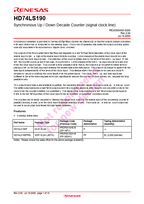
HD74LS190Synchronous Up / Down Decade Counter (signal clock line)REJ03D0452–0200Rev.2.00Jul.15.2005 Synchronous operation is provided by having all flip-flops clocked simultaneously so that the outputs change coincident with each other when so instructed by the steering logic. This mode of operation eliminates the output counting spikes normally associated with asynchronous (ripple clock) counters.The outputs of the four master-slave flip-flops are triggered on a low-to-high-level transition of the clock input if the enable input is low. A high at the enable input inhibits counting. Level changes at the enable input should be made only when the clock input is high. The direction of the count is determined by the level of the down / up input. When low, the counter counts up and when high, it counts down. Level changes at the down / up input should be made only when the clock input is high. This counter is fully programmable; that is, the outputs may be preset to either level by placing a low on the load input and entering the desired data at the data inputs. The output will change to agree with the data inputs independently of the level of the clock input. This feature allows the counters to be used as modulo-N dividers by simply modifying the count length with the preset inputs. The clock, down / up, and load inputs are buffered to lower the drive requirement which significantly reduces the number of clock drivers, etc., required for long parallel words.Two outputs have been made available to perform the cascading function: ripple clock and maximum / minimum count. The latter output produces a high-level output pulse with a duration approximately equal to one complete cycles to the clock when the counter overflows or underflows. The ripple clock output produces a low-level output pulse equal in width to the low-level portion of the clock input when an overflow or underflow conditions exists.The counters can be easily cascaded by feeding the ripple clock output to the enable input of the succeeding counter if parallel clocking is used, or to the clock input if parallel enabling is used. The maximum / minimum count output can be used to accomplish look-ahead for high-speed operation.Features• Ordering InformationPart Name Package Type Package Code(Previous Code)PackageAbbreviationTaping Abbreviation(Quantity)HD74LS190P DILP-16pin PRDP0016AE-B(DP-16FV)P —HD74LS190FPEL SOP-16 pin (JEITA) PRSP0016DH-B(FP-16DAV)FP EL (2,000 pcs/reel)Notes: Please consult the sales office for the above package availability.Pin Arrangement(Top view)Block DiagramClearPreset CK J Q B Q B K ClearPreset CK J Q C Q C K ClearPreset CK J Q D Q D KAbsolute Maximum RatingsItem Symbol Ratings UnitSupply voltage V CC 7 V Input voltage V IN 7 VPower dissipation P T 400 mW Storage temperatureTstg–65 to +150°CNote: Voltage value, unless otherwise noted, are with respect to network ground terminal.Recommended Operating ConditionsItem Symbol Min Typ Max UnitSupply voltage V CC 4.75 5.00 5.25 V I OH — — –400 µAOutput current I OL — — 8 mA Operating temperature T opr –20 25 75 °CClock frequency ƒclock 0 — 20 MHz Clock pulse width t w (CK) 25 — — ns Load pulse width t w (Load) 35 — — ns Setup time t su 20 — — ns Hold time t h (data)3 — — nsEnable time t enable 40 — — nsElectrical Characteristics(Ta = –20 to +75 °C)ItemSymbol min. typ.* max. Unit ConditionV IH 2.0 — — V Input voltageV IL — — 0.8 V V OH 2.7 — — VV CC = 4.75 V, V IH = 2 V, V IL = 0.8 V,I OH = –400 µΑ— — 0.4 I OL = 4 mA Output voltageV OL — — 0.5 VI OL = 8 mA V CC = 4.75 V, V IH = 2 V,V IL = 0.8 VEnable — — 60Others I IH — — 20 µA V CC = 5.25 V, V I = 2.7 VEnable — — –1.2Others I IL — — –0.4 mA V CC = 5.25 V, V I = 0.4 VEnable — — 0.3InputcurrentOthers I I — — 0.1mA V CC = 5.25 V, V I = 7 VShort-circuit outputcurrentI OS –20 — –100 mA V CC = 5.25 VSupply current** I CC — 20 35 mA V CC = 5.25 V Input clamp voltage V IK — — –1.5 V V CC = 4.75 V, I IN = –18 mA Notes: * V CC = 5 V, Ta = 25°C ** I CC is measured with all outputs open and all inputs grounded.Switching Characteristics(V CC = 5 V, Ta = 25°C) Item SymbolInputsOutputs min.typ.max.UnitConditionMaximum clock frequency ƒmax ClockQ A, Q B, Q C, Q D 20 25 — MHzt PLH —2233 t PHLLoad Q A, Q B, Q C, Q D— 33 50nst PLH —2032 t PHLA, B,C, DQ A, Q B, Q C, Q D— 27 40nst PLH —1320 t PHLClock RippleClock— 16 24nst PLH —1624 t PHLClock Q A, Q B, Q C, Q D— 24 36nst PLH —2842 t PHLClock Max / Min— 37 52nst PLH —3045 t PHLDown /UpRipple Clock— 30 45nst PLH —2133 t PHLDown /UpMax / Min— 22 33nst PLH —2133Propagation delay timet PHL Enable RippleClock— 22 33nsC L = 15 pF,R L = 2 kΩCount Sequences7890LoadRipple ClockInhibitCount DownCount Up 12221098Max/Min Q C Q DQ B Illustrated below is the following sequence: Load (preset) to BCD seven. Count up to eight, nine (maximum), zero, one and two. 3. Inhibit Count down to one, zero (minimum), nine, eight, and seven.Testing MethodTest CircuitS e e T e s t i n g A B C D LoadQ AQ BQ CQ DSame as Load Circuit 1.Same as Load Circuit 1.OutputSame as Load Circuit 1.Output Same as Load Circuit 1.Output includes probe and jig capacitance. All diodes are 1S2074(H).Waveforms 11.3V 1.3V 1.3V 1.3Vt THLt TLHt sut su10%10%90%90%90%90%Waveforms 3→Ripple CK, Down / Up→Ripple CK, Down / Up→Max / MinRipple/Clock1.3V1.3V1.3V 1.3V 1.3V 1.3V1.3V1.3Vt PHL t PLH t PHL t PLHEnable = 0V 1.3V 1.3Vt PLHt PHLWhen test the Q A, Q B, and Q C outputs, data inputs A, B and C are shown by the solid line, anddata input D is shown by the dashed line.When test the Q D output, data inputs A and D are shown by the solid line, and data inputs Band C are held at the low logic level.Waveforms 5B, C, DPackage Dimensions1p1e b A LAecθ( Ni/Pd/Au plating )FP-16DAVRENESAS Code Previous Code 0.24gMASS[Typ.]PRSP0016DH-B*2E9FDEH pcb NOTE)1. DIMENSIONS"*1 (Nom)"AND"DO NOT INCLUDE MOLD FLASH.2. DIMENSION"*3"DOES NOT INCLUDE TRIM OFFSET.元器件交易网 RENESAS SALES OFFICESRefer to "/en/network" for the latest and detailed information.Renesas Technology America, Inc.450 Holger Way, San Jose, CA 95134-1368, U.S.ATel: <1> (408) 382-7500, Fax: <1> (408) 382-7501Renesas Technology Europe LimitedDukes Meadow, Millboard Road, Bourne End, Buckinghamshire, SL8 5FH, U.K.Tel: <44> (1628) 585-100, Fax: <44> (1628) 585-900Renesas Technology Hong Kong Ltd.7th Floor, North Tower, World Finance Centre, Harbour City, 1 Canton Road, Tsimshatsui, Kowloon, Hong KongTel: <852> 2265-6688, Fax: <852> 2730-6071Renesas Technology Taiwan Co., Ltd.10th Floor, No.99, Fushing North Road, Taipei, TaiwanTel: <886> (2) 2715-2888, Fax: <886> (2) 2713-2999Renesas Technology (Shanghai) Co., Ltd.Unit2607 Ruijing Building, No.205 Maoming Road (S), Shanghai 200020, ChinaTel: <86> (21) 6472-1001, Fax: <86> (21) 6415-2952Renesas Technology Singapore Pte. Ltd.1 Harbour Front Avenue, #06-10, Keppel Bay Tower, Singapore 098632Tel: <65> 6213-0200, Fax: <65> 6278-8001Renesas Technology Korea Co., Ltd.Kukje Center Bldg. 18th Fl., 191, 2-ka, Hangang-ro, Yongsan-ku, Seoul 140-702, KoreaTel: <82> 2-796-3115, Fax: <82> 2-796-2145Renesas Technology Malaysia Sdn. Bhd.Unit 906, Block B, Menara Amcorp, Amcorp Trade Centre, No.18, Jalan Persiaran Barat, 46050 Petaling Jaya, Selangor Darul Ehsan, MalaysiaTel: <603> 7955-9390, Fax: <603> 7955-9510© 2005. Renesas Technology Corp., All rights reserved. Printed in Japan.Colophon .3.0。
HD74LS145FPEL中文资料

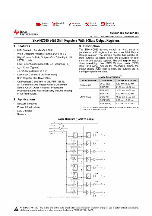
HD74LS145BCD-to-Decimal Decoder / Driver (with 15 V outputs)REJ03D0436–0300Rev.3.00Jul.13.2005This BCD-to-decimal decoder / driver consists of eight inverters and ten four-input NAND gates. The inverters are connected in pairs to make BCD input data available for decoding by the NAND gates. Full decoding of valid BCD input logic ensures that all outputs remain off for all invalid binary input conditions. This decoder features high-performance, n-p-n output transistors designed for use as indicator / relay drivers or as open-collector logic-circuit drivers.Features• Ordering InformationPart Name Package Type Package Code(Previous Code)PackageAbbreviationTaping Abbreviation(Quantity)HD74LS145P DILP-16pin PRDP0016AE-B(DP-16FV)P —HD74LS145FPEL SOP-16 pin (JEITA) PRSP0016DH-B(FP-16DAV)FP EL (2,000 pcs/reel)Note: Please consult the sales office for the above package availability. Pin ArrangementFunction TableInputs OutputsNo. D C B A 0 1 2 3 4 5 6 7 8 9 L L L L L H H H H H H H H H L L L H H L H H H H H H H H L L H L H H L H H H H H H H L L H H H H H L H H H H H H 0 1 2 3 4 L H L L H H H H L H H H H H L H L H H H H H H L H H H H L H H L H H H H H H L H H H L H H H H H H H H H H L H H H L LL H H H H H H H H L H 5 6 7 8 9H L L H H H H H H H H H H L H L H L H H H H H H H H H H H L H H H H H H H H H H H H H H L L H H H H H H H H H H H H L H H H H H H H H H H H H H H L H H H H H H H H H H InvalidH H H H H H H H H H H H H HBlock DiagramAbsolute Maximum RatingsItem Symbol Ratings UnitSupply voltage V CC 7 V Input voltage V IN 7 VPower dissipation P T 400 mW Storage temperatureTstg–65 to +150°CNote: Voltage value, unless otherwise noted, are with respect to network ground terminal.Recommended Operating ConditionsItem Symbol Min Typ Max UnitSupply voltage V CC 4.75 5.00 5.25 V Off-state output voltage V O(off) — — 15 V Low level output current I OL — — 80 mAOperating temperature Topr –20 25 75 °CElectrical Characteristics(Ta = –20 to +75 °C)ItemSymbol min. typ.* max. Unit ConditionV IH 2.0 — — V Input voltage V IL — — 0.8 V Off-state outputcurrent I O(off) —— 250 µA V CC = 4.75 V, V IH = 2 V, V IL = 0.8 V,V O(off) = 15 V— — 0.4 I OL = 12 mA— — 0.5 I OL = 24 mAOn-state output voltageV O(on) — — 3.0 V I OL = 80 mAV CC = 4.75 V, V IH = 2 V,V IL = 0.8 VI IH — — 20 µA V CC = 5.25 V, V I = 2.7 V I IL — — –0.4 mA V CC = 5.25 V, V I = 0.4 VInput currentI I —— 0.1 mA V CC = 5.25 V, V I = 7 V Supply current** I CC — 7 13 mA V CC = 5.25 V Input clamp voltage V IK — — –1.5 V V CC = 4.75 V, I IN = –18 mA Notes: * V CC = 5 V, Ta = 25°C ** I CC is measured with all outputs open and all inputs grounded.Switching Characteristics(V CC = 5 V, Ta = 25°C)Item Symbol min. typ. max. Unit Conditiont PLH — — 50Propagation delay time t PHL — — 50 ns C L = 45 pF, R L = 665 ΩTesting Method Test CircuitWaveformPackage Dimensions RENESAS SALES OFFICESRefer to "/en/network" for the latest and detailed information.Renesas Technology America, Inc.450 Holger Way, San Jose, CA 95134-1368, U.S.ATel: <1> (408) 382-7500, Fax: <1> (408) 382-7501Renesas Technology Europe LimitedDukes Meadow, Millboard Road, Bourne End, Buckinghamshire, SL8 5FH, U.K.Tel: <44> (1628) 585-100, Fax: <44> (1628) 585-900Renesas Technology Hong Kong Ltd.7th Floor, North Tower, World Finance Centre, Harbour City, 1 Canton Road, Tsimshatsui, Kowloon, Hong KongTel: <852> 2265-6688, Fax: <852> 2730-6071Renesas Technology Taiwan Co., Ltd.10th Floor, No.99, Fushing North Road, Taipei, TaiwanTel: <886> (2) 2715-2888, Fax: <886> (2) 2713-2999Renesas Technology (Shanghai) Co., Ltd.Unit2607 Ruijing Building, No.205 Maoming Road (S), Shanghai 200020, ChinaTel: <86> (21) 6472-1001, Fax: <86> (21) 6415-2952Renesas Technology Singapore Pte. Ltd.1 Harbour Front Avenue, #06-10, Keppel Bay Tower, Singapore 098632Tel: <65> 6213-0200, Fax: <65> 6278-8001Renesas Technology Korea Co., Ltd.Kukje Center Bldg. 18th Fl., 191, 2-ka, Hangang-ro, Yongsan-ku, Seoul 140-702, KoreaTel: <82> 2-796-3115, Fax: <82> 2-796-2145Renesas Technology Malaysia Sdn. Bhd.Unit 906, Block B, Menara Amcorp, Amcorp Trade Centre, No.18, Jalan Persiaran Barat, 46050 Petaling Jaya, Selangor Darul Ehsan, MalaysiaTel: <603> 7955-9390, Fax: <603> 7955-9510。
HD74LS04P中文资料

HD74LS04P中⽂资料HD74LS04 / HD74LS05Hex Inverters / Hex Inverters (with Open Collector Outputs) REJ03D0391–0300Rev.3.00Jul.13.2005 FeaturesOrdering InformationHD74LS04Part Name Package Type Package Code(Previous Code)PackageAbbreviationTaping Abbreviation(Quantity)HD74LS04P DILP-14pin PRDP0014AB-B(DP-14AV)P —HD74LS04FPEL SOP-14 pin (JEITA) PRSP0014DF-B (FP-14DAV)FP EL (2,000 pcs/reel)HD74LS04RPEL SOP-14 pin (JEDEC) PRSP0014DE-A (FP-14DNV)RP EL (2,500 pcs/reel)HD74LS05Part Name Package Type Package Code(Previous Code)PackageAbbreviationTaping Abbreviation(Quantity)HD74LS05P DILP-14pin PRDP0014AB-B(DP-14AV)P —HD74LS05FPEL SOP-14 pin (JEITA) PRSP0014DF-B(FP-14DAV)FP EL (2,000 pcs/reel)HD74LS05RPEL SOP-14 pin (JEDEC) PRSP0014DE-A(FP-14DNV)RP EL (2,500 pcs/reel)Note: Please consult the sales office for the above package availability. Pin ArrangementCircuit Schematic (1/6)Absolute Maximum RatingsUnitRatingsItem SymbolSupply voltage V CC Note 7 VInput voltage V IN 7 V Power dissipation P T 400 mW Storage temperature Tstg –65 to +150 °C Note: Voltage value, unless otherwise noted, are with respect to network ground terminal. Recommended Operating ConditionsHD74LS04MaxUnitMinTypItem SymbolSupply voltage V CC 4.75 5.00 5.25 VI OH — — –400 µAOutput currentI OL — — 8 mA°C2575Operating temperature Topr–20HD74LS05MaxUnitTypMinItem SymbolSupply voltage V CC 4.75 5.00 5.25 VOutput voltage V OH — — 5.5 VOutput current I OL — — 8 mA°C7525–20Operating temperature ToprElectrical CharacteristicsHD74LS04(Ta = –20 to +75 °C)ItemSymbol min. typ.* max. Unit Condition V IH 2.0 — — V Input voltageV IL — — 0.8 V V OH 2.7 — — V V CC = 4.75 V, V IL = 0.8 V, I OH = –400 µA — — 0.5 I OL = 8 mAOutput voltageV OL— — 0.4 V I OL = 4 mAV CC = 4.75 V, V IH = 2 V I IH — — 20 µA V CC = 5.25 V, V I = 2.7 V I IL — — –0.4 mA V CC = 5.25 V, V I = 0.4 V Input current I I — — 0.1 mA V CC = 5.25 V, V I = 7 V Short-circuit outputcurrent I OS –20— –100 mA V CC = 5.25 V I CCH — 1.2 2.4 mA V CC = 5.25 VSupply currentI CCL — 3.6 6.6 mA V CC = 5.25 VInput clamp voltage V IK — — –1.5 V V CC = 4.75 V, I IN = –18 mA Note: * V CC = 5 V, Ta = 25°CHD74LS05(Ta = –20 to +75 °C)ItemSymbol min. typ.* max. Unit Condition V IH 2.0 — — VInput voltageV IL — — 0.8 V— — 0.5 I OL = 8 mAOutput voltage V OL — — 0.4 V I OL = 4 mAV CC = 4.75 V, V IH = 2 VOutput current I OH — — 100 µA V CC = 4.75 V, V IL = 0.8 V, V OA = 5.5 VI IH — — 20 µA V CC = 5.25 V, V I = 2.7 VI IL — — –0.4 mA V CC = 5.25 V, V I = 0.4 VInput current I I —— 0.1 mA V CC = 5.25 V, V I = 7 V I CCH — 1.2 2.4 mA V CC = 5.25 VSupply currentI CCL —3.6 6.6 mA V CC = 5.25 V Input clamp voltage V IK — — –1.5 V V CC =4.75 V, I IN = –18 mA Note: * V CC = 5 V, Ta = 25°CSwitching CharacteristicsHD74LS04(V CC = 5 V, Ta = 25°C)Item Symbol min. typ. max. Unit Conditiont PLH — 9 15 nsPropagation delay timet PHL — 10 15 ns C L = 15 pF, R L = 2 k ?HD74LS05(V CC = 5 V, Ta = 25°C)Item Symbol min. typ. max. Unit Conditiont PLH — 17 32 nsPropagation delay time t PHL — 15 28 nsC L = 15 pF, R L = 2 k ?Note: Refer to Test Circuit and Waveform of the Common Item "TTL Common Matter (Document No.: REJ27D0005-0100)". Package Dimensions/doc/1d43150d90c69ec3d4bb7502.html RENESAS SALES OFFICESRefer to "/doc/1d43150d90c69ec3d4bb7502.html /en/network" for the latest and detailed information. Renesas Technology America, Inc.450 Holger Way, San Jose, CA 95134-1368, U.S.ATel: <1> (408) 382-7500, Fax: <1> (408) 382-7501Renesas Technology Europe LimitedDukes Meadow, Millboard Road, Bourne End, Buckinghamshire, SL8 5FH, U.K.Tel: <44> (1628) 585-100, Fax: <44> (1628) 585-900Renesas Technology Hong Kong Ltd.7th Floor, North Tower, World Finance Centre, Harbour City, 1 Canton Road, Tsimshatsui, Kowloon, Hong KongTel: <852> 2265-6688, Fax: <852> 2730-6071Renesas Technology Taiwan Co., Ltd.10th Floor, No.99, Fushing North Road, Taipei, TaiwanTel: <886> (2) 2715-2888, Fax: <886> (2) 2713-2999Renesas Technology (Shanghai) Co., Ltd.Unit2607 Ruijing Building, No.205 Maoming Road (S), Shanghai 200020, ChinaTel: <86> (21) 6472-1001, Fax: <86> (21) 6415-2952Renesas Technology Singapore Pte. Ltd.1 Harbour Front Avenue, #06-10, Keppel Bay Tower, Singapore 098632Tel: <65> 6213-0200, Fax: <65> 6278-8001Renesas Technology Korea Co., Ltd.Kukje Center Bldg. 18th Fl., 191, 2-ka, Hangang-ro, Yongsan-ku, Seoul 140-702, KoreaTel: <82> 2-796-3115, Fax: <82> 2-796-2145Renesas Technology Malaysia Sdn. Bhd.Unit 906, Block B, Menara Amcorp, Amcorp Trade Centre, No.18, Jalan Persiaran Barat, 46050 Petaling Jaya, Selangor Darul Ehsan, MalaysiaTel: <603> 7955-9390, Fax: <603> 7955-9510。
HD74LS14P中文资料

HD74LS14Hex Schmitt Trigger InvertersREJ03D0399–0300Rev.3.00Jul.13.2005 Features• Ordering InformationPart Name Package Type Package Code(Previous Code)PackageAbbreviationTaping Abbreviation(Quantity)HD74LS14P DILP-14pin PRDP0014AB-B(DP-14AV)P —HD74LS14FPEL SOP-14 pin (JEITA) PRSP0014DF-B(FP-14DAV)FP EL (2,000 pcs/reel)Note: Please consult the sales office for the above package availability. Pin ArrangementCircuit Schematic (1/6)Absolute Maximum RatingsUnit Item SymbolRatingsInput voltage V IN 7 V Supply voltage V CC 7 V Power dissipation P T 400mW Storage temperature Tstg –65 to +150 °CNote: Voltage value, unless otherwise noted, are with respect to network ground terminal.Recommended Operating ConditionsUnitMaxItem SymbolMinTypSupply voltage V CC 4.75 5.00 5.25 VI OH — — –400 µAOutput currentI OL — — 8 mA°C7525–20Operating temperature ToprElectrical Characteristics(Ta = –20 to +75 °C)ItemSymbol min. typ.* max. Unit ConditionV T +1.4 1.6 1.9 V V CC = 5 V Input thresholdvoltage V T –0.5 0.7 1.0 VV CC = 5 V Hysteresis V T + – V T –0.4 0.9 — V V CC = 5 VV OH 2.7 — — V V CC = 4.75 V, V I = 0.5 V, I OH = –400 µA— — 0.5 I OL = 8 mAOutput voltage V OL— — 0.4 V I OL = 4 mAV CC = 4.75 V, V I = 1.9 V I T + — –0.14 — mA V CC = 5 V, V I = V T + Input thresholdcurrent I T –— –0.18 — mA V CC = 5 V, V I = V T – I IH — — 20 µA V CC = 5.25 V, V I = 2.7 VI IL — — –0.4 mA V CC = 5.25 V, V I = 0.4 VInput current I I — — 0.1 mA V CC = 5.25 V, V I = 7 V Short-circuit outputcurrent I OS –20— –100 mA V CC = 5.25 V I CCH — 8.6 16 mA V CC = 5.25 VSupply currentI CCL — 12 21 mA V CC = 5.25 VInput clamp voltage V IK — — –1.5 V V CC = 4.75 V, I IN = –18 mANote: * V CC = 5 V, Ta = 25°CSwitching Characteristics(V CC = 5 V, Ta = 25°C)Item Symbol min. typ. max. Unit Conditiont PLH — 15 22 nsPropagation delay time t PHL — 15 22 ns C L = 15 pF, R L = 2 k ΩTesting Method Test CircuitWaveformPackage Dimensions RENESAS SALES OFFICESRefer to "/en/network" for the latest and detailed information.Renesas Technology America, Inc.450 Holger Way, San Jose, CA 95134-1368, U.S.ATel: <1> (408) 382-7500, Fax: <1> (408) 382-7501Renesas Technology Europe LimitedDukes Meadow, Millboard Road, Bourne End, Buckinghamshire, SL8 5FH, U.K.Tel: <44> (1628) 585-100, Fax: <44> (1628) 585-900Renesas Technology Hong Kong Ltd.7th Floor, North Tower, World Finance Centre, Harbour City, 1 Canton Road, Tsimshatsui, Kowloon, Hong KongTel: <852> 2265-6688, Fax: <852> 2730-6071Renesas Technology Taiwan Co., Ltd.10th Floor, No.99, Fushing North Road, Taipei, TaiwanTel: <886> (2) 2715-2888, Fax: <886> (2) 2713-2999Renesas Technology (Shanghai) Co., Ltd.Unit2607 Ruijing Building, No.205 Maoming Road (S), Shanghai 200020, ChinaTel: <86> (21) 6472-1001, Fax: <86> (21) 6415-2952Renesas Technology Singapore Pte. Ltd.1 Harbour Front Avenue, #06-10, Keppel Bay Tower, Singapore 098632Tel: <65> 6213-0200, Fax: <65> 6278-8001Renesas Technology Korea Co., Ltd.Kukje Center Bldg. 18th Fl., 191, 2-ka, Hangang-ro, Yongsan-ku, Seoul 140-702, KoreaTel: <82> 2-796-3115, Fax: <82> 2-796-2145Renesas Technology Malaysia Sdn. Bhd.Unit 906, Block B, Menara Amcorp, Amcorp Trade Centre, No.18, Jalan Persiaran Barat, 46050 Petaling Jaya, Selangor Darul Ehsan, MalaysiaTel: <603> 7955-9390, Fax: <603> 7955-9510。
HD74LS14FPEL中文资料

HD74LS14Hex Schmitt Trigger InvertersREJ03D0399–0300Rev.3.00Jul.13.2005 Features• Ordering InformationPart Name Package Type Package Code(Previous Code)PackageAbbreviationTaping Abbreviation(Quantity)HD74LS14P DILP-14pin PRDP0014AB-B(DP-14AV)P —HD74LS14FPEL SOP-14 pin (JEITA) PRSP0014DF-B(FP-14DAV)FP EL (2,000 pcs/reel)Note: Please consult the sales office for the above package availability. Pin ArrangementCircuit Schematic (1/6)Absolute Maximum RatingsUnit Item SymbolRatingsInput voltage V IN 7 V Supply voltage V CC 7 V Power dissipation P T 400mW Storage temperature Tstg –65 to +150 °CNote: Voltage value, unless otherwise noted, are with respect to network ground terminal.Recommended Operating ConditionsUnitMaxItem SymbolMinTypSupply voltage V CC 4.75 5.00 5.25 VI OH — — –400 µAOutput currentI OL — — 8 mA°C7525–20Operating temperature ToprElectrical Characteristics(Ta = –20 to +75 °C)ItemSymbol min. typ.* max. Unit ConditionV T +1.4 1.6 1.9 V V CC = 5 V Input thresholdvoltage V T –0.5 0.7 1.0 VV CC = 5 V Hysteresis V T + – V T –0.4 0.9 — V V CC = 5 VV OH 2.7 — — V V CC = 4.75 V, V I = 0.5 V, I OH = –400 µA— — 0.5 I OL = 8 mAOutput voltage V OL— — 0.4 V I OL = 4 mAV CC = 4.75 V, V I = 1.9 V I T + — –0.14 — mA V CC = 5 V, V I = V T + Input thresholdcurrent I T –— –0.18 — mA V CC = 5 V, V I = V T – I IH — — 20 µA V CC = 5.25 V, V I = 2.7 VI IL — — –0.4 mA V CC = 5.25 V, V I = 0.4 VInput current I I — — 0.1 mA V CC = 5.25 V, V I = 7 V Short-circuit outputcurrent I OS –20— –100 mA V CC = 5.25 V I CCH — 8.6 16 mA V CC = 5.25 VSupply currentI CCL — 12 21 mA V CC = 5.25 VInput clamp voltage V IK — — –1.5 V V CC = 4.75 V, I IN = –18 mANote: * V CC = 5 V, Ta = 25°CSwitching Characteristics(V CC = 5 V, Ta = 25°C)Item Symbol min. typ. max. Unit Conditiont PLH — 15 22 nsPropagation delay time t PHL — 15 22 ns C L = 15 pF, R L = 2 k ΩTesting Method Test CircuitWaveformPackage Dimensions RENESAS SALES OFFICESRefer to "/en/network" for the latest and detailed information.Renesas Technology America, Inc.450 Holger Way, San Jose, CA 95134-1368, U.S.ATel: <1> (408) 382-7500, Fax: <1> (408) 382-7501Renesas Technology Europe LimitedDukes Meadow, Millboard Road, Bourne End, Buckinghamshire, SL8 5FH, U.K.Tel: <44> (1628) 585-100, Fax: <44> (1628) 585-900Renesas Technology Hong Kong Ltd.7th Floor, North Tower, World Finance Centre, Harbour City, 1 Canton Road, Tsimshatsui, Kowloon, Hong KongTel: <852> 2265-6688, Fax: <852> 2730-6071Renesas Technology Taiwan Co., Ltd.10th Floor, No.99, Fushing North Road, Taipei, TaiwanTel: <886> (2) 2715-2888, Fax: <886> (2) 2713-2999Renesas Technology (Shanghai) Co., Ltd.Unit2607 Ruijing Building, No.205 Maoming Road (S), Shanghai 200020, ChinaTel: <86> (21) 6472-1001, Fax: <86> (21) 6415-2952Renesas Technology Singapore Pte. Ltd.1 Harbour Front Avenue, #06-10, Keppel Bay Tower, Singapore 098632Tel: <65> 6213-0200, Fax: <65> 6278-8001Renesas Technology Korea Co., Ltd.Kukje Center Bldg. 18th Fl., 191, 2-ka, Hangang-ro, Yongsan-ku, Seoul 140-702, KoreaTel: <82> 2-796-3115, Fax: <82> 2-796-2145Renesas Technology Malaysia Sdn. Bhd.Unit 906, Block B, Menara Amcorp, Amcorp Trade Centre, No.18, Jalan Persiaran Barat, 46050 Petaling Jaya, Selangor Darul Ehsan, MalaysiaTel: <603> 7955-9390, Fax: <603> 7955-9510。
74LS148中文资料
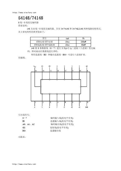
CT54LS148/CT74LS148
15ns
60mW
148 将 8 条数据线(0-7)进行 3 线(4-2-1)二进制(八进制)优先编
码,即对最高位数据线进行译码。
利用选通端(EI)和输出选通端(EO)可进行八进制扩展。
管脚图:
引出端符号: 0-7 EI A0、A1、A2 GS EO
功能表:
编码输入端(低电平有效) 选通输入端(低电平有效) 编码输出端(低电平有效) 宽展端(低电平有效) 选通输出端
http://www.elecfans.com
http://www.elecfans.com
说明:H-高电平 L-低电平 X-任意
极限值 电源电压------------------------------------------------7V 输入电压 54/74148-----------------------------------------5.5V 54/74LS148--------------------------------------7V 发射极间电压 54/74148 的两编码输入----------------------------5.5V 工作环境温度 54×××------------------------------ -55~125℃ 74×××------------------------------------0~70℃ 贮存温度-------------------------------------- -65~150℃
tPHL
(同相输出)
tPLH
EI->GS
tPHL
(同相输出)
tPLH
EI->EO
tPHL
74LS148四路抢答器设计报告
74LS148四路抢答器设计报告潍坊学院专业课综合课程设计说明书设计题目:四路抢答器设计系部:信息与控制工程学院专业:电气自动化技术班级:一班学生姓名:2013年6月10日目录1.设计任务和要求 (3)2.设计方案 (3)2.1设计思路 (3)2.2设计原理 (4)2.3实现功能 (4)3.硬件设计 (5)3.1各功能电路连线图 (5)3.2框图和说明 (6)4.软件设计 (7)5.小结 (8)6.参考文献 (9)1设计任务与要求1.1 可同时供四名选手参赛,其编号分别是1-4,各用一个抢答按钮,按钮的编号和选手的编号相对应,给节目主持人设置一控制开关,用于控制系统的清零(编号显示数码管灭灯)抢答的开始。
1.2 抢答器具有数据锁存和显示的功能,抢答开始后,若有选手按抢答按钮,其编号立即所存,并在数码管上显示该选手的编号,同时封锁输入电路,禁止其他选手抢答。
优先抢答选手的编号一直保持到主持人主持人将系统清零为止。
2 设计方案2.1 设计思路2.1.1 在给定5V直流电源电压的条件下设计一个可以容纳四组参赛者的抢答器,每组设定一个抢答按钮供参赛者使用。
2.1.2 设置一个系统清零和抢答控制开关K(该开关由主持人控制),当开关K 被按下时,抢答开始(允许抢答),打开后抢答电路清零。
2.1.3 抢答器具有一个抢答信号的鉴别、锁存及显示功能。
即有抢答信号输入(参赛者的开关中任意一个开关被按下)时,锁存相应的编号,并在LED数码管上显示出来,同时扬声器发生声响。
此时再按其他任何一个抢答器开关均无效,优先抢答选手的编号一直保持不变,直到主持人将系统清除为止。
2.1.4 开关K按下后,抢答开始,开始10S倒计时。
2.2 设计原理2.2.1原理图2.2.2 设计原理接通电源后,主持人将开关拨到"清除"状态,抢答器处于禁止状态,编号显示器灭灯,定时器显示设定时间;主持人将开关置“开始"状态,宣布"开始"抢答器工作。
74LS148中文资料_数据手册_参数
HD74LS248P中文资料

Hitachi CodeJEDECEIAJWeight (reference value)DP-16 Conforms Conforms 1.07 gHitachi Code JEDEC EIAJWeight (reference value)FP-16DA —Conforms 0.24 g*Dimension including the plating thicknessBase material dimension° – 8°Hitachi CodeJEDECEIAJWeight (reference value)FP-16DNConformsConforms0.15 gUnit: mm*Dimension including the plating thickness Base material dimension° – 8°元器件交易网Cautions1.Hitachi neither warrants nor grants licenses of any rights of Hitachi’s or any third party’s patent,copyright, trademark, or other intellectual property rights for information contained in this document.Hitachi bears no responsibility for problems that may arise with third party’s rights, includingintellectual property rights, in connection with use of the information contained in this document.2.Products and product specifications may be subject to change without notice. Confirm that you have received the latest product standards or specifications before final design, purchase or use.3.Hitachi makes every attempt to ensure that its products are of high quality and reliability. However,contact Hitachi’s sales office before using the product in an application that demands especially high quality and reliability or where its failure or malfunction may directly threaten human life or cause risk of bodily injury, such as aerospace, aeronautics, nuclear power, combustion control, transportation,traffic, safety equipment or medical equipment for life support.4.Design your application so that the product is used within the ranges guaranteed by Hitachi particularly for maximum rating, operating supply voltage range, heat radiation characteristics, installationconditions and other characteristics. Hitachi bears no responsibility for failure or damage when used beyond the guaranteed ranges. Even within the guaranteed ranges, consider normally foreseeable failure rates or failure modes in semiconductor devices and employ systemic measures such as fail-safes, so that the equipment incorporating Hitachi product does not cause bodily injury, fire or other consequential damage due to operation of the Hitachi product.5.This product is not designed to be radiation resistant.6.No one is permitted to reproduce or duplicate, in any form, the whole or part of this document without written approval from Hitachi.7.Contact Hitachi’s sales office for any questions regarding this document or Hitachi semiconductor products.Hitachi, Ltd.Semiconductor & Integrated Circuits.Nippon Bldg., 2-6-2, Ohte-machi, Chiyoda-ku, Tokyo 100-0004, Japan Tel: Tokyo (03) 3270-2111 Fax: (03) 3270-5109Copyright ' Hitachi, Ltd., 1999. All rights reserved. Printed in Japan.Hitachi Asia Pte. Ltd.16 Collyer Quay #20-00Hitachi TowerSingapore 049318Tel: 535-2100Fax: 535-1533URLNorthAmerica : http:/Europe : /hel/ecg Asia (Singapore): .sg/grp3/sicd/index.htm Asia (Taiwan): /E/Product/SICD_Frame.htm Asia (HongKong): /eng/bo/grp3/index.htm Japan : http://www.hitachi.co.jp/Sicd/indx.htmHitachi Asia Ltd.Taipei Branch Office3F, Hung Kuo Building. No.167, Tun-Hwa North Road, Taipei (105)Tel: <886> (2) 2718-3666Fax: <886> (2) 2718-8180Hitachi Asia (Hong Kong) Ltd.Group III (Electronic Components)7/F., North Tower, World Finance Centre,Harbour City, Canton Road, Tsim Sha Tsui,Kowloon, Hong Kong Tel: <852> (2) 735 9218Fax: <852> (2) 730 0281 Telex: 40815 HITEC HXHitachi Europe Ltd.Electronic Components Group.Whitebrook ParkLower Cookham Road MaidenheadBerkshire SL6 8YA, United Kingdom Tel: <44> (1628) 585000Fax: <44> (1628) 778322Hitachi Europe GmbHElectronic components Group Dornacher Stra§e 3D-85622 Feldkirchen, Munich GermanyTel: <49> (89) 9 9180-0Fax: <49> (89) 9 29 30 00Hitachi Semiconductor (America) Inc.179 East Tasman Drive,San Jose,CA 95134 Tel: <1> (408) 433-1990Fax: <1>(408) 433-0223For further information write to:。
HD74HC283P中文资料
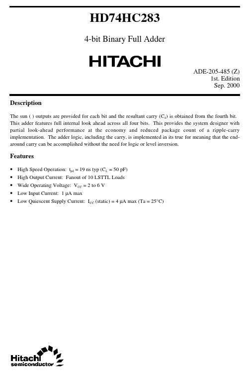
HD74HC2834-bit Binary Full AdderADE-205-485 (Z)1st. EditionSep. 2000 Description) is obtained from the fourth bit. The sun () outputs are provided for each bit and the resultant carry (C4This adder features full internal look ahead across all four bits. This provides the system designer with partial look-ahead performance at the economy and reduced package count of a ripple-carry implementation. The adder logic, including the carry, is implemented in its true for meaning that the end-around carry can be accomplished without the need for logic or level inversion.Features• High Speed Operation: t pd = 19 ns typ (C L = 50 pF)• High Output Current: Fanout of 10 LSTTL Loads• Wide Operating Voltage: V CC = 2 to 6 V• Low Input Current: 1 µA max• Low Quiescent Supply Current: I CC (static) = 4 µA max (Ta = 25°C)HD74HC2832Function TableOutputsInputs When C 0 = L/When C 2 = L When C 0 = H/When C 2 = H A 1/A 3B 1/B 3A 2/A 4B 2/B 4∑1/∑3∑2/∑4C 2/C 4∑1/∑3∑2/∑4C 2/C 4L L L L L L L H L L H L L L H L L L H L L H L L H L L L H L H H L L L H L H H L L L H L L H L H H L H L H L H H L L L H L H H L H H L L L H H H H L L L H H L H L L L H L H L H H L H L L H H H L L L H L H L H H H L L L H H H L H L L H H L H L L H H L L H H L H H L H H H L H L H H L H H H H L H L H H HHHHLHHHHHH :high level L :low levelNote:Input conditions at A 1, B 1, A 2, B 2, and C 0 are used to determine outputs ∑1 and ∑2 and the value of theinternal carry C 2. The values at C 2, A 3, B 3, A 4 and B4 are then used to determine outputs ∑3, ∑4 and C 4.HD74HC283 Pin Arrangement3HD74HC283 Block Diagram4HD74HC2835DC CharacteristicsTa = 25°CTa = –40 to +85°CItem Symbol V CC (V)Min Typ Max MinMax Unit Test ConditionsInput voltageV IH2.0 1.5—— 1.5—V4.5 3.15—— 3.15—6.04.2—— 4.2—V IL2.0——0.5—0.5V 4.5—— 1.35—1.356.0——1.8— 1.8Output voltageV OH2.0 1.9 2.0— 1.9—VVin = V IH or V IL I OH = –20 µA4.5 4.4 4.5— 4.4—6.05.96.0— 5.9—4.5 4.18—— 4.13—I OH = –4 mA 6.05.68——5.63—I OH = –5.2 mAV OL2.0—0.00.1—0.1VVin = V IH or V IL I OL = 20 µA4.5—0.00.1—0.16.0—0.00.1—0.14.5——0.26—0.33I OL = 4 mA 6.0——0.26—0.33I OL = 5.2 mAInput current Iin 6.0——±0.1—±1.0µA Vin = V CC or GNDQuiescent supply currentI CC6.0——4.0—40µAVin = V CC or GND, Iout = 0 µAHD74HC2836AC Characteristics (C L = 50 pF, Input t r = t f = 6 ns)Ta = 25°CTa = –40 to +85°CItem Symbol V CC (V)Min Typ Max MinMax Unit Test Conditions Propagation delay t PLH2.0——150—190nsC 0 to ∑1timet PHL 4.5—1930—386.0——26—33t PLH 2.0——150—190nsA 1 orB 1 to ∑1t PHL 4.5—1930—386.0——26—33t PLH 2.0——150—190nsC 0 to C 4t PHL 4.5—1930—386.0——26—33t PLH 2.0——150—190nsA 1 orB 1 toC 4t PHL4.5—1930—386.0——26—33Output rise/fall t TLH 2.0——75—95ns timet THL 4.5—515—196.0——13—16Input capacitanceCin——510—10pFHD74HC283 Package Dimensions7HD74HC2838HD74HC2839Cautions1.Hitachi neither warrants nor grants licenses of any rights of Hitachi’s or any third party’s patent,copyright, trademark, or other intellectual property rights for information contained in this document.Hitachi bears no responsibility for problems that may arise with third party’s rights, includingintellectual property rights, in connection with use of the information contained in this document.2.Products and product specifications may be subject to change without notice. Confirm that you have received the latest product standards or specifications before final design, purchase or use.3.Hitachi makes every attempt to ensure that its products are of high quality and reliability. However,contact Hitachi’s sales office before using the product in an application that demands especially high quality and reliability or where its failure or malfunction may directly threaten human life or cause risk of bodily injury, such as aerospace, aeronautics, nuclear power, combustion control, transportation,traffic, safety equipment or medical equipment for life support.4.Design your application so that the product is used within the ranges guaranteed by Hitachi particularly for maximum rating, operating supply voltage range, heat radiation characteristics, installationconditions and other characteristics. Hitachi bears no responsibility for failure or damage when used beyond the guaranteed ranges. Even within the guaranteed ranges, consider normally foreseeable failure rates or failure modes in semiconductor devices and employ systemic measures such as fail-safes, so that the equipment incorporating Hitachi product does not cause bodily injury, fire or other consequential damage due to operation of the Hitachi product.5.This product is not designed to be radiation resistant.6.No one is permitted to reproduce or duplicate, in any form, the whole or part of this document without written approval from Hitachi.7.Contact Hitachi’s sales office for any questions regarding this document or Hitachi semiconductor products.Hitachi, Ltd.Semiconductor & Integrated Circuits.Nippon Bldg., 2-6-2, Ohte-machi, Chiyoda-ku, Tokyo 100-0004, Japan Tel: Tokyo (03) 3270-2111 Fax: (03) 3270-5109Copyright © Hitachi, Ltd., 2000. All rights reserved. Printed in Japan.Hitachi Asia Ltd. Hitachi Tower16 Collyer Quay #20-00, Singapore 049318Tel : <65>-538-6533/538-8577 Fax : <65>-538-6933/538-3877URL : .sg URLNorthAmerica : /Europe : /hel/ecg Asia : Japan : http://www.hitachi.co.jp/Sicd/indx.htmHitachi Asia Ltd.(Taipei Branch Office)4/F, No. 167, Tun Hwa North Road, Hung-Kuo Building, Taipei (105), Taiwan Tel : <886>-(2)-2718-3666 Fax : <886>-(2)-2718-8180 Telex : 23222 HAS-TPURL : Hitachi Asia (Hong Kong) Ltd. Group III (Electronic Components) 7/F., North Tower, World Finance Centre,Harbour City, Canton Road Tsim Sha Tsui, Kowloon, Hong KongTel : <852>-(2)-735-9218 Fax : <852>-(2)-730-0281URL : Hitachi Europe Ltd.Electronic Components Group.Whitebrook ParkLower Cookham Road MaidenheadBerkshire SL6 8YA, United Kingdom Tel: <44> (1628) 585000Fax: <44> (1628) 585160Hitachi Europe GmbHElectronic Components Group Dornacher Stra βe 3D-85622 Feldkirchen, Munich GermanyTel: <49> (89) 9 9180-0Fax: <49> (89) 9 29 30 00Hitachi Semiconductor (America) Inc.179 East Tasman Drive,San Jose,CA 95134 Tel: <1> (408) 433-1990Fax: <1>(408) 433-0223For further information write to:Colophon 2.0。
74ls系列中文资料功能介绍

74ls系列中文资料功能介绍(注:红色为实验室已有器件)型号功能----------------------------------------------------74ls00 2输入四与非门74ls01 2输入四与非门(oc)74ls02 2输入四或非门74ls03 2输入四与非门(oc)74ls04 六倒相器74ls05 六倒相器(oc)74ls06 六高压输出反相缓冲器/驱动器(oc,30v) 74ls07 六高压输出缓冲器/驱动器(oc,30v)74ls08 2输入四与门74ls09 2输入四与门(oc)74ls10 3输入三与非门74ls11 3输入三与门74ls12 3输入三与非门(oc)74ls13 4输入双与非门(斯密特触发)74ls14 六倒相器(斯密特触发)74ls15 3输入三与门(oc)74ls16 六高压输出反相缓冲器/驱动器(oc,15v) 74ls17 六高压输出缓冲器/驱动器(oc,15v)74ls18 4输入双与非门(斯密特触发)74ls19 六倒相器(斯密特触发)74ls20 4输入双与非门74ls21 4输入双与门74ls22 4输入双与非门(oc)74ls23 双可扩展的输入或非门74ls24 2输入四与非门(斯密特触发)74ls25 4输入双或非门(有选通)74ls26 2输入四高电平接口与非缓冲器(oc,15v) 74ls27 3输入三或非门74ls28 2输入四或非缓冲器74ls30 8输入与非门74ls31 延迟电路74ls32 2输入四或门74ls33 2输入四或非缓冲器(集电极开路输出)74ls34 六缓冲器74ls35 六缓冲器(oc)74ls36 2输入四或非门(有选通)74ls37 2输入四与非缓冲器74ls38 2输入四或非缓冲器(集电极开路输出)74ls39 2输入四或非缓冲器(集电极开路输出)74ls40 4输入双与非缓冲器74ls41 bcd-十进制计数器74ls42 4线-10线译码器(bcd输入)74ls43 4线-10线译码器(余3码输入)74ls44 4线-10线译码器(余3葛莱码输入)74ls45 bcd-十进制译码器/驱动器74ls46 bcd-七段译码器/驱动器74ls47 bcd-七段译码器/驱动器74ls48 bcd-七段译码器/驱动器74ls49 bcd-七段译码器/驱动器(oc)74ls50 双二路2-2输入与或非门(一门可扩展)74ls51 双二路2-2输入与或非门74ls51 二路3-3输入,二路2-2输入与或非门74ls52 四路2-3-2-2输入与或门(可扩展)74ls53 四路2-2-2-2输入与或非门(可扩展)74ls53 四路2-2-3-2输入与或非门(可扩展)74ls54 四路2-2-2-2输入与或非门74ls54 四路2-3-3-2输入与或非门74ls54 四路2-2-3-2输入与或非门74ls55 二路4-4输入与或非门(可扩展)74ls60 双四输入与扩展74ls61 三3输入与扩展74ls62 四路2-3-3-2输入与或扩展器74ls63 六电流读出接口门74ls64 四路4-2-3-2输入与或非门74ls65 四路4-2-3-2输入与或非门(oc)74ls70 与门输入上升沿jk触发器74ls71 与输入r-s主从触发器74ls72 与门输入主从jk触发器74ls73 双j-k触发器(带清除端)74ls74 正沿触发双d型触发器(带预置端和清除端)74ls75 4位双稳锁存器74ls76 双j-k触发器(带预置端和清除端)74ls77 4位双稳态锁存器74ls78 双j-k触发器(带预置端,公共清除端和公共时钟端) 74ls80 门控全加器74ls81 16位随机存取存储器74ls82 2位二进制全加器(快速进位)74ls83 4位二进制全加器(快速进位)74ls84 16位随机存取存储器74ls85 4位数字比较器74ls86 2输入四异或门74ls87 四位二进制原码/反码/oi单元74ls89 64位读/写存储器74ls90 十进制计数器74ls91 八位移位寄存器74ls92 12分频计数器(2分频和6分频)74ls93 4位二进制计数器74ls94 4位移位寄存器(异步)74ls95 4位移位寄存器(并行io)74ls96 5位移位寄存器74ls97 六位同步二进制比率乘法器74ls100 八位双稳锁存器74ls103 负沿触发双j-k主从触发器(带清除端)74ls106 负沿触发双j-k主从触发器(带预置,清除,时钟) 74ls107 双j-k主从触发器(带清除端)74ls108 双j-k主从触发器(带预置,清除,时钟)74ls109 双j-k触发器(带置位,清除,正触发)74ls110 与门输入j-k主从触发器(带锁定)74ls111 双j-k主从触发器(带数据锁定)74ls112 负沿触发双j-k触发器(带预置端和清除端)74ls113 负沿触发双j-k触发器(带预置端)74ls114 双j-k触发器(带预置端,共清除端和时钟端)74ls116 双四位锁存器74ls120 双脉冲同步器/驱动器74ls121 单稳态触发器(施密特触发)74ls122 可再触发单稳态多谐振荡器(带清除端)74ls123 可再触发双单稳多谐振荡器74ls125 四总线缓冲门(三态输出)74ls126 四总线缓冲门(三态输出)74ls128 2输入四或非线驱动器74ls131 3-8译码器74ls132 2输入四与非门(斯密特触发)74ls133 13输入端与非门74ls134 12输入端与门(三态输出)74ls135 四异或/异或非门74ls136 2输入四异或门(oc)74ls137 八选1锁存译码器/多路转换器74ls138 3-8线译码器/多路转换器74ls139 双2-4线译码器/多路转换器74ls140 双4输入与非线驱动器74ls141 bcd-十进制译码器/驱动器74ls142 计数器/锁存器/译码器/驱动器74ls145 4-10译码器/驱动器74ls147 10线-4线优先编码器74ls148 8线-3线八进制优先编码器74ls150 16选1数据选择器(反补输出)74ls151 8选1数据选择器(互补输出)74ls152 8选1数据选择器多路开关74ls153 双4选1数据选择器/多路选择器74ls154 4线-16线译码器74ls155 双2-4译码器/分配器(图腾柱输出)74ls156 双2-4译码器/分配器(集电极开路输出) 74ls157 四2选1数据选择器/多路选择器74ls158 四2选1数据选择器(反相输出)74ls160 可预置bcd计数器(异步清除)74ls161 可预置四位二进制计数器(并清除异步) 74ls162 可预置bcd计数器(异步清除)74ls163 可预置四位二进制计数器(并清除异步) 74ls164 8位并行输出串行移位寄存器74ls165 并行输入8位移位寄存器(补码输出) 74ls166 8位移位寄存器74ls167 同步十进制比率乘法器74ls168 4位加/减同步计数器(十进制)74ls169 同步二进制可逆计数器74ls170 4*4寄存器堆74ls171 四d触发器(带清除端)74ls172 16位寄存器堆74ls173 4位d型寄存器(带清除端)74ls174 六d触发器74ls175 四d触发器74ls176 十进制可预置计数器74ls177 2-8-16进制可预置计数器74ls178 四位通用移位寄存器74ls179 四位通用移位寄存器74ls180 九位奇偶产生/校验器74ls181 算术逻辑单元/功能发生器74ls182 先行进位发生器74ls183 双保留进位全加器74ls184 bcd-二进制转换器74ls185 二进制-bcd转换器74ls190 同步可逆计数器(bcd,二进制)74ls191 同步可逆计数器(bcd,二进制)74ls192 同步可逆计数器(bcd,二进制)74ls193 同步可逆计数器(bcd,二进制)74ls194 四位双向通用移位寄存器74ls195 四位通用移位寄存器74ls196 可预置计数器/锁存器74ls197 可预置计数器/锁存器(二进制)74ls198 八位双向移位寄存器74ls199 八位移位寄存器74ls210 2-5-10进制计数器74ls213 2-n-10可变进制计数器74ls221 双单稳触发器74ls230 八3态总线驱动器74ls231 八3态总线反向驱动器74ls240 八缓冲器/线驱动器/线接收器(反码三态输出) 74ls241 八缓冲器/线驱动器/线接收器(原码三态输出) 74ls242 八缓冲器/线驱动器/线接收器74ls243 4同相三态总线收发器74ls244 八缓冲器/线驱动器/线接收器74ls245 八双向总线收发器74ls246 4线-七段译码/驱动器(30v)74ls247 4线-七段译码/驱动器(15v)74ls248 4线-七段译码/驱动器74ls249 4线-七段译码/驱动器74ls251 8选1数据选择器(三态输出)74ls253 双四选1数据选择器(三态输出)74ls256 双四位可寻址锁存器74ls257 四2选1数据选择器(三态输出)74ls258 四2选1数据选择器(反码三态输出)74ls259 8为可寻址锁存器74ls260 双5输入或非门74ls261 4*2并行二进制乘法器74ls265 四互补输出元件74ls266 2输入四异或非门(oc)74ls270 2048位rom (512位四字节,oc)74ls271 2048位rom (256位八字节,oc)74ls273 八d触发器74ls274 4*4并行二进制乘法器74ls275 七位片式华莱士树乘法器74ls276 四jk触发器74ls278 四位可级联优先寄存器74ls279 四s-r锁存器74ls280 9位奇数/偶数奇偶发生器/较验器74ls28174ls283 4位二进制全加器74ls290 十进制计数器74ls291 32位可编程模74ls293 4位二进制计数器74ls294 16位可编程模74ls295 四位双向通用移位寄存器74ls298 四-2输入多路转换器(带选通)74ls299 八位通用移位寄存器(三态输出)74ls348 8-3线优先编码器(三态输出)74ls352 双四选1数据选择器/多路转换器74ls353 双4-1线数据选择器(三态输出)74ls354 8输入端多路转换器/数据选择器/寄存器,三态补码输出74ls355 8输入端多路转换器/数据选择器/寄存器,三态补码输出74ls356 8输入端多路转换器/数据选择器/寄存器,三态补码输出74ls357 8输入端多路转换器/数据选择器/寄存器,三态补码输出74ls365 6总线驱动器74ls366 六反向三态缓冲器/线驱动器74ls367 六同向三态缓冲器/线驱动器74ls368 六反向三态缓冲器/线驱动器74ls373 八d锁存器74ls374 八d触发器(三态同相)74ls375 4位双稳态锁存器74ls377 带使能的八d触发器74ls378 六d触发器74ls379 四d触发器74ls381 算术逻辑单元/函数发生器74ls382 算术逻辑单元/函数发生器74ls384 8位*1位补码乘法器74ls385 四串行加法器/乘法器74ls386 2输入四异或门74ls390 双十进制计数器74ls391 双四位二进制计数器74ls395 4位通用移位寄存器74ls396 八位存储寄存器74ls398 四2输入端多路开关(双路输出)74ls399 四-2输入多路转换器(带选通)74ls422 单稳态触发器74ls423 双单稳态触发器74ls440 四3方向总线收发器,集电极开路74ls441 四3方向总线收发器,集电极开路74ls442 四3方向总线收发器,三态输出74ls443 四3方向总线收发器,三态输出74ls444 四3方向总线收发器,三态输出74ls445 bcd-十进制译码器/驱动器,三态输出74ls446 有方向控制的双总线收发器74ls448 四3方向总线收发器,三态输出74ls449 有方向控制的双总线收发器74ls465 八三态线缓冲器74ls466 八三态线反向缓冲器74ls467 八三态线缓冲器74ls468 八三态线反向缓冲器74ls490 双十进制计数器74ls540 八位三态总线缓冲器(反向)74ls541 八位三态总线缓冲器74ls589 有输入锁存的并入串出移位寄存器74ls590 带输出寄存器的8位二进制计数器74ls591 带输出寄存器的8位二进制计数器74ls592 带输出寄存器的8位二进制计数器74ls593 带输出寄存器的8位二进制计数器74ls594 带输出锁存的8位串入并出移位寄存器74ls595 8位输出锁存移位寄存器74ls596 带输出锁存的8位串入并出移位寄存器74ls597 8位输出锁存移位寄存器74ls598 带输入锁存的并入串出移位寄存器74ls599 带输出锁存的8位串入并出移位寄存器74ls604 双8位锁存器74ls605 双8位锁存器74ls606 双8位锁存器74ls607 双8位锁存器74ls620 8位三态总线发送接收器(反相)74ls621 8位总线收发器74ls622 8位总线收发器74ls623 8位总线收发器74ls640 反相总线收发器(三态输出)74ls641 同相8总线收发器,集电极开路74ls642 同相8总线收发器,集电极开路74ls643 8位三态总线发送接收器74ls644 真值反相8总线收发器,集电极开路74ls645 三态同相8总线收发器74ls646 八位总线收发器,寄存器74ls647 八位总线收发器,寄存器74ls648 八位总线收发器,寄存器74ls649 八位总线收发器,寄存器74ls651 三态反相8总线收发器74ls652 三态反相8总线收发器74ls653 反相8总线收发器,集电极开路74ls654 同相8总线收发器,集电极开路74ls668 4位同步加/减十进制计数器74ls669 带先行进位的4位同步二进制可逆计数器74ls670 4*4寄存器堆(三态)74ls671 带输出寄存的四位并入并出移位寄存器74ls672 带输出寄存的四位并入并出移位寄存器74ls673 16位并行输出存储器,16位串入串出移位寄存器74ls674 16位并行输入串行输出移位寄存器74ls681 4位并行二进制累加器74ls682 8位数值比较器(图腾柱输出)74ls683 8位数值比较器(集电极开路)74ls684 8位数值比较器(图腾柱输出)74ls685 8位数值比较器(集电极开路)74ls686 8位数值比较器(图腾柱输出)74ls687 8位数值比较器(集电极开路)74ls688 8位数字比较器(oc输出)74ls689 8位数字比较器74ls690 同步十进制计数器/寄存器(带数选,三态输出,直接清除)74ls691 计数器/寄存器(带多转换,三态输出)74ls692 同步十进制计数器(带预置输入,同步清除)74ls693 计数器/寄存器(带多转换,三态输出)74ls696 同步加/减十进制计数器/寄存器(带数选,三态输出,直接清除) 74ls697 计数器/寄存器(带多转换,三态输出)74ls698 计数器/寄存器(带多转换,三态输出)74ls699 计数器/寄存器(带多转换,三态输出)74ls716 可编程模n十进制计数器74ls718 可编程模n十进制计数器。
74LS148中文资料_数据手册_参数

74ls148管脚图引脚功能表真值表逻辑图扩展

74ls148管脚图引脚功能表真值表逻辑图扩展资料有些单片机控制系统和数字电路中,无法对几个按钮的同时响应做出反映,如电梯控制系统在这种情况下就出出现错误,这是绝对不允许的。
于是就出现了74ls148优先编码器,先说一下他的基本原理.他允许同时输入两个以上编码信号。
不过在设计优先编码器时已经将所有的输入信号按优先顺序排了队,当几个输入信号同时出现时,只对其中优先权最高的一个进行编码。
〈74ls148管脚功能〉〈74ls148引脚图〉74ls148优先编码器管脚功能介绍:为16脚的集成芯片,电源是VCC(16) GND(8), I0—I7为输入信号,A2,A1,A0为三位二进制编码输出信号,IE是使能输入端,OE是使能输出端,GS为片优先编码输出端。
〈74ls148逻辑图〉〈74ls148逻辑表达式〉使能端OE(芯片是否启用)的逻辑方程:OE =I0·I1·I2·I3·I4·I5·I6·I7·IE当OE输入IE=1时,禁止编码、输出(反码):A2,A1,A0为全1。
当OE输入IE=0时,允许编码,在I0~I7输入中,输入I7优先级最高,其余依次为:I6,I5,I4,I3,I2,I0,I0等级排列。
输入输出EI I0I1I2I3I4I5I6I7A2A1AGS EO1x x x x x x x x11111 01111111111110 0x x x x x x x000001 0x x x x x x0100110 0x x x x x01101010 0x x x x011101110 0x x x0111110010 0x x01111110110 0x011111111010 00111111111110<优先编码器74ls148功能表>从以上的的功能表中可以得出,74ls148输入端优先级别的次序依次为I7,I 6,…,I0 。
74ls148管脚图引脚功能表真值表逻
74ls148管脚图引脚功能表真值表逻
有些单片机控制系统和数字电路中,无法对几个按钮的同时响应做出反映,如电梯控制系统在这种情况下就出出现错误,这是绝对不允许的。
于是就出现了74ls148优先编码器,先说一下他的基本原理.他允许同时输入两个以上编码信号。
不过在设计优先编码器时已经将所有的输入信号按优先顺序排了队,当几个输入信号同时出现时,只对其中优先权最高的一个进行编码。
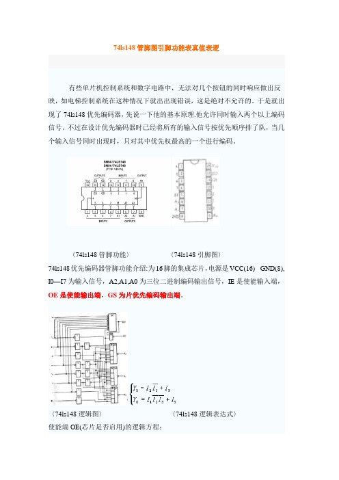
〈74ls148管脚功能〉〈74ls148引脚图〉
74ls148优先编码器管脚功能介绍:为16脚的集成芯片,电源是VCC(16) GND(8), I0—I7为输入信号,A2,A1,A0为三位二进制编码输出信号,IE是使能输入端,OE是使能输出端,GS为片优先编码输出端。
〈74ls148逻辑图〉〈74ls148逻辑表达式〉
使能端OE(芯片是否启用)的逻辑方程:
<74ls148真值表>
由74ls148真值表可列输出逻辑方程为:
A2 = (I4+I5+I6+I7)IE
A1 = (I2I4I5+I3I4I5+I6+7)·IE
A0 = (I1I2I4I6+I3I4I6+I5I6+I7)·IE
用两个74ls148优先编码器芯片扩展为十六线-四线优先编码器的电路连线图。
实验二 8线——3线优先编码器74LS148功能测试及应用
数字电子技术基础实验报告
实验二8线——3线优先编码器74LS148功能测试及应用
专业班级姓名学号成绩通信工程一班赵建倪201409110134
一、实验目的
了解8线——3线优先编码(74LS148)的基本功能;
掌握74LS148的使用方法;
二、实验内容
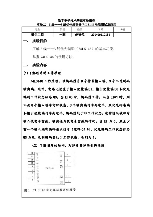
(1)了解芯片的工作原理
74LS148工作原理:该编码器有8个信号输入端,3个二进制码输出端。
此外,电路还设置了输入使能端EI,输出使能端EO和优先编码工作状态标志GS。
当EI=0时,编码器工作;而当EI=1时,则不论8个输入端为何种状态,3个输出端均为高电平,且优先标志端和输出使能端均为高电平,编码器处于非工作状态。
这种情况被称为输入低电平有效,输出也为低电来有效的情况。
当EI为0,且至少有一个输入端有编码请求信号(逻辑0)时,优先编码工作状态标志GS为0。
表明编码器处于工作状态,否则为1。
(2)了解芯片的结构,对照着具体的引脚接线
(3)验证优先编码器的真值表
真值表。
ls148管脚图引脚功能表真值表逻辑图扩展 (1)
74ls148管脚图引脚功能表真值表逻辑图扩展资料有些单片机控制系统和数字电路中,无法对几个按钮的同时响应做出反映,如电梯控制系统在这种情况下就出出现错误,这是绝对不允许的。
于是就出现了74ls148优先编码器,先说一下他的基本原理.他允许同时输入两个以上编码信号。
不过在设计优先编码器时已经将所有的输入信号按优先顺序排了队,当几个输入信号同时出现时,只对其中优先权最高的一个进行编码。
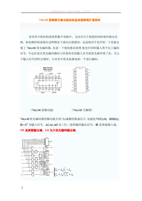
〈74ls148管脚功能〉〈74ls148引脚图〉74ls148优先编码器管脚功能介绍:为16脚的集成芯片,电源是VCC(16) GND(8), I0—I7为输入信号,A2,A1,A0为三位二进制编码输出信号,IE是使能输入端,OE是使能输出端,GS为片优先编码输出端。
〈74ls148逻辑图〉〈74ls148逻辑表达式〉使能端OE(芯片是否启用)的逻辑方程:OE =I0·I1·I2·I3·I4·I5·I6·I7·IE当OE输入IE=1时,禁止编码、输出(反码):A2,A1,A0为全1。
当OE输入IE=0时,允许编码,在I0~I7输入中,输入I7优先级最高,其余依次为:I6,I5,I4,I3,I2,I0,I0等级排列。
输入输出EI I0I1I2I3I4I5I6I7A2A1AGSEO1x x x x x x x x11111 01111111111110 0x x x x x x x000001 0x x x x x x0100110 0x x x x x01101010 0x x x x011101110 0x x x0111110010 0x x01111110110 0x011111111010 00111111111110<优先编码器74ls148功能表>从以上的的功能表中可以得出,74ls148输入端优先级别的次序依次为I7,I 6,…,I0 。
集成芯片的功能
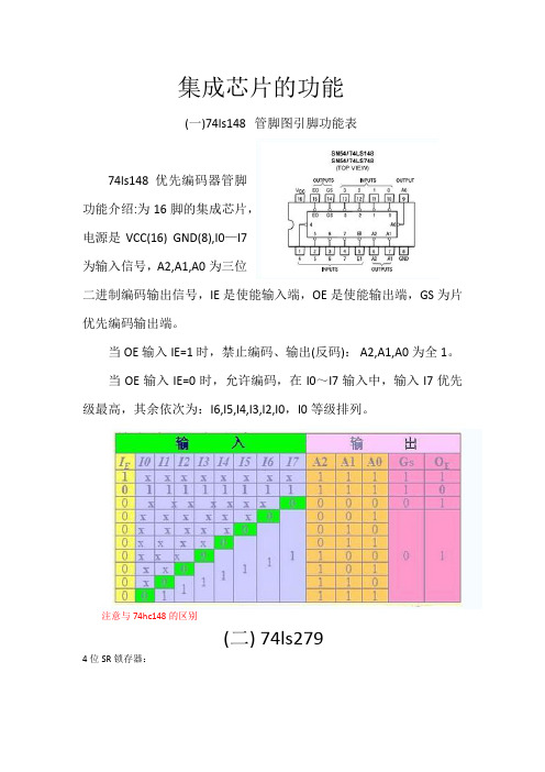
集成芯片的功能(一)74ls148 管脚图引脚功能表74ls148优先编码器管脚功能介绍:为16脚的集成芯片,电源是VCC(16) GND(8),I0—I7为输入信号,A2,A1,A0为三位二进制编码输出信号,IE是使能输入端,OE是使能输出端,GS为片优先编码输出端。
当OE输入IE=1时,禁止编码、输出(反码): A2,A1,A0为全1。
当OE输入IE=0时,允许编码,在I0~I7输入中,输入I7优先级最高,其余依次为:I6,I5,I4,I3,I2,I0,I0等级排列。
注意与74hc148的区别(二) 74ls2794位SR锁存器:(三)74ls48高电平输出有效译码器,用于输出高低电平驱动数码管显示输出端(Ya-Yg)为高电平有效,可驱动灯缓冲器或共阴极VLED。
当要求输出 0-15 时,消隐输入(BI)应为高电平或开路,对于输出为0 时还要求脉冲消隐输入(RBI)为高电平或者开路。
当BI为低电平时,不管其它输入端状态如何,Ya-Yg均为低电平。
当RBI和地址端(A0-A3)均为低电平,并且灯测试输入端(LT)为高电平时, Ya -Yg为低电平,脉冲消隐输出(RBO)也变为低电平。
当BI为高电平或开路时,LT为低电平可使Ya-Yg均为高电平。
48 与248 的引出端排列、功能和电特性均相同,差别仅在显示6 和9,248 所显示的6 和9 比48 多出上杠和下杠。
引出端符号A0-A3 译码地址输入端BI/RBO消隐输入(低电平有效)/脉冲消隐输出(低电平有效)LT灯测试输入端(低电平有效)RBI脉冲消隐输入端(低电平有效)Ya-Yg 段输出54121/74121单稳态触发器(有施密特触发器)简要说明:54/74121为具有施密特触发器输入的单稳态触发器,其主要电特性的典型值如下:型号输出脉冲范围 PD CT54121/CT7412140ns->28s90mW正触发输入端(B)采用了施密特触发器,因此,有较高的抗扰度,典型值为1.2V。
- 1、下载文档前请自行甄别文档内容的完整性,平台不提供额外的编辑、内容补充、找答案等附加服务。
- 2、"仅部分预览"的文档,不可在线预览部分如存在完整性等问题,可反馈申请退款(可完整预览的文档不适用该条件!)。
- 3、如文档侵犯您的权益,请联系客服反馈,我们会尽快为您处理(人工客服工作时间:9:00-18:30)。
HD74LS1488-line-to-3-line Octal Priority EncoderREJ03D0437–0200Rev.2.00Feb.18.2005The HD74LS148 encodes eight data lines to three-line (4-2-1) binary (octal). Cascading circuitry (enable input EI and enable output EO) has been provided to allow octal expansion without the need for external circuitry. The data inputs and outputs are active at the low logic level.Features• Ordering InformationPart Name Package Type Package Code(Previous Code)PackageAbbreviationTaping Abbreviation(Quantity)HD74LS148P DILP-16pin PRDP0016AE-B(DP-16FV)P —HD74LS148FPEL SOP-16 pin (JEITA) PRSP0016DH-B(FP-16DAV)FP EL (2,000 pcs/reel)Note: Please consult the sales office for the above package availability. Pin ArrangementFunction TableInputs OutputsEI 0 1 2 3 4 5 6 7 A2 A1 A0 GS EO H X X X X X X X X H H H H H L H H H H H H H H H H H H L L X X X X X X X L L L L L H L X X X X X X L H L L H L H L X X X X X L H H L H L L H L X X X X L H H H L H H L H L X X X L H H H H H L L L H L X X L H H H H H H L H L H LX L H H H H H H H H L L H L L H H H H H H H H H H L H H ; high level, L ; low level, X ; irrelevantBlock DiagramAbsolute Maximum RatingsItem Symbol Ratings UnitSupply voltage V CC 7 V Input voltage V IN 7 VPower dissipation P T 400 mW Storage temperatureTstg–65 to +150°CNote: Voltage value, unless otherwise noted, are with respect to network ground terminal.Recommended Operating ConditionsItem Symbol Min Typ Max UnitSupply voltage V CC 4.75 5.00 5.25 V I OH — — –400 µAOutput current I OL — — 8 mA Operating temperature Topr–20 25 75 °CElectrical Characteristics(Ta = –20 to +75 °C)ItemSymbol min. typ.* max. UnitConditionV IH 2.0 — — V Input voltageV IL — — 0.8 VV OH 2.7 — — VV CC = 4.75 V, V IH = 2 V, V IL = 0.8 V, I OH = –400 µA— — 0.4 I OL = 4 mA Output voltageV OL — — 0.5 VI OL = 8 mA V CC = 4.75 V, V IH = 2 V,V IL = 0.8 V 1 to 7 Inputs — — 40Other inputs I IH — — 20µA V CC = 5.25 V, V I = 2.7 V1 to 7 Inputs — — –0.8Other inputs I IL — — –0.4 mA V CC = 5.25 V, V I = 0.4 V1 to 7 Inputs — — 0.2Input currentOther inputsI I— — 0.1mA V CC = 5.25 V, V I = 7 VShort-circuit output currentI OS –20 — –100 mA V CC = 5.25 V — 12 20 mA Condition 1Supply current**I CC— 10 17 mA Condition 2V CC = 5.25 VInput clamp voltage V IK — — –1.5 V V CC = 4.75 V, I IN = –18 mA Notes: * V CC = 5 V, Ta = 25°C ** The condition 1 is measured with inputs 7 and EI grounded, other inputs and outputs open, the condition 2 ismeasured with all inputs and outputs open.Switching Characteristics(V CC = 5 V, Ta = 25°C)Item Symbol min. typ. max. Unit Inputs OutputsOutputWaveformsConditiont PLH — 14 18 t PHL — 15 25ns 0 to 7A 0, A 1or A 2 In-phase Output t PLH — 20 36 t PHL — 16 29ns 0 to 7A 0, A 1or A 2 Out-of-phaseOutput t PLH — 7 18t PHL — 25 40 ns 0 to 7 EOOut-of-phase Output t PLH — 35 55t PHL — 9 21 ns 0 to 7 GSIn-phase Output t PLH — 16 25 t PHL — 12 25ns EIA 0, A 1or A 2 In-phase Outputt PLH — 12 17 t PHL — 14 36ns EI GSIn-phaseOutput t PLH — 12 21 Propagation delay timet PHL — 23 35ns EI EOIn-phaseOutput C L = 15 pF,R L = 2 k ΩTesting Method Test CircuitWaveformPackage Dimensions RENESAS SALES OFFICESRefer to "/en/network" for the latest and detailed information.Renesas Technology America, Inc.450 Holger Way, San Jose, CA 95134-1368, U.S.ATel: <1> (408) 382-7500, Fax: <1> (408) 382-7501Renesas Technology Europe LimitedDukes Meadow, Millboard Road, Bourne End, Buckinghamshire, SL8 5FH, U.K.Tel: <44> (1628) 585-100, Fax: <44> (1628) 585-900Renesas Technology Hong Kong Ltd.7th Floor, North Tower, World Finance Centre, Harbour City, 1 Canton Road, Tsimshatsui, Kowloon, Hong KongTel: <852> 2265-6688, Fax: <852> 2730-6071Renesas Technology Taiwan Co., Ltd.10th Floor, No.99, Fushing North Road, Taipei, TaiwanTel: <886> (2) 2715-2888, Fax: <886> (2) 2713-2999Renesas Technology (Shanghai) Co., Ltd.Unit2607 Ruijing Building, No.205 Maoming Road (S), Shanghai 200020, ChinaTel: <86> (21) 6472-1001, Fax: <86> (21) 6415-2952Renesas Technology Singapore Pte. Ltd.1 Harbour Front Avenue, #06-10, Keppel Bay Tower, Singapore 098632Tel: <65> 6213-0200, Fax: <65> 6278-8001。
