Circular Polarization Switchable Microstrip Antenna
压电、热释电与铁电材料

关于BaTiO3铁电性的起因人们曾提出过多种 微观模型。其中比较突出的有: 钛离子多个平衡位置的自发极化理论,认 为BaTiO3在其顺电相结构中钛离子具有多 个平衡位置,在温度低于居里点时,钛离 子占据某个平衡位置几率大得多,因而出 现自发极化;
钛--氧离子之间的强耦合理论,认为自发 极化的产生是由于钛--氧离子之间存在着 很强的相互作用场所致; 此外换有氧离子位移的自发极化理论;振 动电子理论;价键性质转变理论(认为共 价性增强,离子性减弱)等。 这些理论各有其不足和成功之处,本节不 在一一介绍。
下图是180畴壁和90畴壁
钛酸钡畴结构
反铁电体
反铁电体是这样一些晶体,晶体结构与同 型铁电体相近,但相邻离子沿反平行方向 产生自发极化,净自发极化强度为零,不 存在类似于铁电中的电滞回线。介电常数 (或极化率)与温度的关系为:在相变温 度以下,介电常数很小,一般数量级为10102;在相变温度时,介电常数出现峰值, 一般数量级为几千。在相变温度以上,介 电常数与温度的关系遵从居里-外斯定律。
主要特征 电滞回线hysteresis loop 居里温度Curie temperature c 介电反常Dielectric anomalous
电滞回线 hysteresis loop
自发极化Ps 剩余极化Pr 矫顽电场Ec
静态畴结构及其形成原因
铁电晶体在没有外电场和外力作用下从 顺电相过渡到铁电相时,将出现至少两 个等价的自发极化方向,以便使晶体的 总自由能最小。因此,晶体在铁电相通 常是由自发极化方向不同的一个一个小 区域组成。每一个极化方向相同的小区 域称为铁电畴,分离电畴的边界称为畴 壁。Domain wall
BaTiO3铁电相变的微观理论首先是从离子位 移模型出发而发展起来的。对BaTiO3晶体的 x射线衍射和中子衍射实验表明,当BaTiO3 的结构从立方相转变到四方相时,Ti、O等 离子都产生偏离原来平衡位置的位移。
Hayati_et_al-2013-Microwave_and_Optical_Technology_Letters
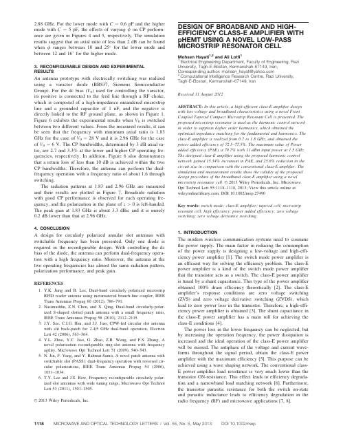
2.88GHz.For the lower mode with C¼0.6pF and the higher mode with C¼5pF,the effects of varying/on CP perform-ance are given in Figures4and5,respectively.The simulation results suggest that an axial ratio of less than2dB can be found when/ranges between10and25 for the lower mode and between12and16 for the higher mode.3.RECONFIGURABLE DESIGN AND EXPERIMENTAL RESULTSAn antenna prototype with electrically switching was realized using a varactor diode(BB837,Siemens Semiconductor Group).For the dc bias(V0)used for controlling the varactor, its positive is connected to the feed line through a RF choke, which is composed of a high-impedance meandered microstrip line and a grounded capacitor of1nF,and the negative is directly linked to the RF ground plane,as shown in Figure1. Figure6exhibits the experimental results when V0is switched between two different values.From the measured results,it can be seen that the frequency with minimum axial ratio is1.83 GHz for the case of V0¼28V and it is2.96GHz for the case of V0¼6V.The CP bandwidths,determined by3dB axial ra-tio,are2.7and3.3%at the lower and higher CP operating fre-quencies,respectively.In addition,Figure6also demonstrates that a return loss of less than10dB is achieved within the two CP bandwidths.Therefore,the antenna can perform the dual-frequency operation with a frequency ratio of about1.6through switching.The radiation patterns at1.83and2.96GHz are measured and their results are plotted in Figure7.Broadside radiation with good CP performance is observed for each operating fre-quency,and the polarization in the plane of z>0is left-handed. The peak gain at1.83GHz is about3.3dBic and it is merely 0.2dB lower than that at2.96GHz.4.CONCLUSIONA design for circularly polarized annular slot antennas with switchable frequency has been presented.Only one diode is required in the reconfigurable design.With controlling the dc bias of the diode,the antenna can perform dual-frequency opera-tion with a high frequency ratio.Moreover,the antenna at the two operating frequencies has almost the same radiation pattern, polarization performance,and peak gain.REFERENCES1.Y.K.Jung and B.Lee,Dual-band circularly polarized microstripRFID reader antenna using metamaterial branch-line coupler,IEEE Trans Antennas Propag60(2012),786–791.2.Nasimuddin,Z.N.Chen,and X.Qing,Dual-band circularly-polar-ized S-shaped slotted patch antenna with a small frequency ratio, IEEE Trans Antennas Propag58(2010),2112–2115.3.J.Y.Sze,C.I.G.Hsu,and J.J.Jiao,CPW-fed circular slot antennawith slit back-patch for2.4/5GHz dual-band operation,Electron Lett42(2006),563–564.4.Y.L.Zhao,Y.C.Jiao,G.Zhao,Z.B.Weng,and F.S.Zhang,Anovel polarization reconfigurable ring-slot antenna with frequency agility,Microwave Opt Technol Lett51(2009),540–543.5.N.Jin,F.Yang,and Y.Rahmat-Samii,A novel patch antenna withswitchable slot(PASS):dual-frequency operation with reversed cir-cular polarizations,IEEE Trans Antennas Propag54(2006), 1031–1034.6.T.Y.Lee and J.S.Row,Frequency reconfigurable circularly polar-ized slot antennas with wide tuning range,Microwave Opt Technol Lett53(2011),1501–1505.V C2013Wiley Periodicals,Inc.DESIGN OF BROADBAND AND HIGH-EFFICIENCY CLASS-E AMPLIFIER WITH pHEMT USING A NOVEL LOW-PASS MICROSTRIP RESONATOR CELLMohsen Hayati1,2and Ali Lotfi11Electrical Engineering Department,Faculty of Engineering,Razi University,Tagh-E-Bostan,Kermanshah-67149,Iran; Corresponding author:mohsen_hayati@2Computational Intelligence Research Centre,Razi University,Tagh-E-Bostan,Kermanshah-67149,IranReceived31August2012ABSTRACT:In this article,a high-efficient class-E amplifier design with low voltage and broadband characteristics using a novel Front Coupled Tapered Compact Microstrip Resonant Cell is presented.The proposed micorstrip resonator is used as the harmonic control network in order to suppress higher order harmonics,which obtained the optimized impedance matching for the fundamental and harmonics.The class-E amplifier is realized from0.7to1.8GHz,and obtained the power added efficiency of72.5–77.5%.The maximum value of Power added efficiency(PAE)is79.7%with11-dBm input power at1.5GHz. The designed class-E amplifier using the proposed harmonic control network gained15.34%increment in PAE,and25.6%reduction in the circuit size in comparison with the conventional class-E amplifier.The simulation and measurement results show the validity of the proposed design procedure of the broadband class-E amplifier using a novel microstrip resonator cell.V C2013Wiley Periodicals,Inc.Microwave Opt Technol Lett55:1118–1118,2013;View this article online at .DOI10.1002/mop.27490Key words:switch mode;class-E amplifier;tapered cell;microstrip resonant cell;high efficiency;power added efficiency;zero voltage switching;zero voltage derivative switching1.INTRODUCTIONThe modern wireless communication systems need to consume the power supply.The main factor in reducing the consumption of the power supply is designing a low-voltage and high-effi-ciency power amplifier[1].The switch mode power amplifier is an efficient way for solving the efficiency problem.The class-E power amplifier is a kind of the switch mode power amplifier that the transistor acts as a switch.The class-E power amplifier is tuned by a shunt capacitance.This type of the power amplifier obtained100%drain efficiency theoretically[2].The class-E amplifier’s response conditions are zero voltage switching (ZVS)and zero voltage derivative switching(ZVDS),which lead to zero power loss in the transistor.Therefore,a high-effi-ciency power amplifier is obtained[3].The shunt capacitance in the class-E power amplifier has a main roll for achieving the class-E conditions[4].The power loss in the lower frequency can be neglected,but by increasing the operation frequency,the power dissipation is increased and the ideal operation of the class-E power amplifier will be missed.The antiphase of the voltage and current wave-forms throughout the signal period,obtain the class-E power amplifier with the maximum efficiency[5].This purpose can be achieved using a wave shaping network.The conventional class-E power amplifier load resistance is very much lower than the transistor ON-resistance.This effect leads to efficiency degrada-tion and a narrowband load matching network[6].Furthermore, the transistor parasitic resistance for both the switch on-state and parasitic inductance leads to efficiency degradation in the radio frequency(RF)and microwave applications[7,8].The optimum operation of the class-E power amplifier and the solution to the mentioned drawbacks can be obtained using two main methods:namely active device selection and circuit configuration[9].The class-E amplifier has various configura-tions such as the cascade[10]and push–pull[11].The cascade class-E configurations can double the maximum permissible drain voltage,and the push–pull class-E configuration increases the output power and decrease the harmonic distortion with high efficiency.A new topology for the class-E amplifier is proposed as an inverse class-E amplifier,which has inductive reactance [12].The inverse class-E amplifier has higher load resistance and lower peak switch voltage in comparison with the class-E amplifier.Also,because of the abruption of the device output inductances,the value of the inductance in the load network is decreased.However,the inverse class-E amplifier can be used only for the small to medium power applications.Therefore,to solve this drawback,the power combining methods have been used[13].Although,this method results in obtaining the inverse class-E amplifier for higher power application,but the circuit configuration and the design procedure are complicated with the circuit size increment because of using two power amplifier circuits.The class-E power amplifier is a high-efficiency power am-plifier for the microwave application,which is implemented using the transmission line as the harmonic control network at the output of the amplifier circuit[14].Furthermore,instead of the RF choke(RFC)a section of the transmission line is used.The transmission line has been used in the class-E power amplifier using LDMOS[15],GaN HEMT[16–19],SiC MES-FET[20],and LDMOSFET[21]as the harmonic control net-work increasingly,because of the simplicity of its structure and high rejection of harmonics.Therefore,the class-E amplifier configuration and operation are the best candidates for the design of the amplifier for the modern microwave communica-tion systems[22,23].Consequently,designing of the load network as the harmonic control network for suppression of harmonics in order to obtain a high-efficiency power amplifier is the main challenge of the switch mode power amplifiers.The designing of the class-E power amplifiers using various microstrip structures has been proposed such as a defected ground structure[24],an asymmet-rical spur-line[25],and composite right/left-handed transmission lines[26].The narrowband load network and low efficiency remain as the main challenge to the class-E power amplifier using the conventional microstrip transmission line[27].A compact microstrip resonant cell(CMRC)is a one-dimen-sional photonic band gap incorporating the microstrip transmis-sion line,which is,first,proposed in[28].The CMRC structure exhibits high rejection of the harmonics with the compact circuit size in comparison with the conventional micorstrip transmission lines.Therefore,it is used for the linearization and efficiency in-crement of the microwave power amplifiers[29,30].The appli-cation of the conventional CMRC is limited to obtain a high-ef-ficiency switch mode amplifier,as a result of the high insertion loss in the passband and restricted stopband.The front coupled tapered CMRC(FCTCMRC)is proposed in[31]for the implan-tation of a low-passfilter with high and wide rejection in the stopband with the compact circuit size in comparison with the conventional CMRC.Therefore,it can be widely used for designing the high-efficiency and broadband switch mode power amplifier because of high and wide suppression of harmonics.In this article,the harmonic suppression of the class-E ampli-fier using a novel FCTCMRC as the harmonic controller net-work is explored.A class-E amplifier with higher efficiency at a wider bandwidth in comparison with the conventional amplifiers is achieved.The proposed class-E power amplifier is designed and simulated for a frequency of1.5GHz using the micorstrip resonator structure.The measurement results of the proposed power amplifier validate our design procedure and simulation results.2.CLASS-E AMPLIFIER FUNDAMENTAL AND DESIGN THEORY2.1.Class-E Amplifier OperationThe basic circuit configuration of the class-E amplifier and switch waveforms are shown in Figures1(a)and1(b),respec-tively.The class-E amplifier consists of the switch device,shunt capacitance,series-tuned load network L-C,and an ideal RFC. The switch-on duty ratio is assumed to be50%in designing the class-E amplifier.This value of the duty ratio leads to optimum operation of the class-E amplifier for obtaining high efficiency [32].For an ideal class-E operation,three requirements for the drain voltage and current should be met[2]:1.The rise of the voltage across the transistor at turn-offshould be delayed until the transistor is off.2.The drain voltage should be brought back to zero at thetime of the transistor turn-on.3.The slope of the drain voltage should be zero at the timeof the transistor turn-on.Therefore,the class-E power amplifier is constructed based on two conditions as ZVS and ZVDS.These conditions are as follows:v s hðÞjh¼p¼0;(1)dv s hðÞd hh¼p¼0;(2)where v s(y)is the switch voltage,and y¼x t.The quality fac-tor of the output series resonant circuit is assumed infinite. Therefore,the output current is sinusoidal asi oðhÞ¼I m sinðhþuÞ:(3)In the time interval0y<p,the switch device is in the on-state,therefore,using Kirchhoff’s current law at the switch,we havei sðhÞ¼I dc1þa sin hþuðÞðÞ:(4)This is the currentflow through the shunt capacitance in the switch-off state.Therefore,the voltage across the switchisFigure1(a)The basic circuit of the class-E amplifier.(b)The class-E switch voltage and current waveformv sðtÞ¼1C sZ ti sðt0Þdt0¼I dcx C s1þa cos x tþuðÞÀcos uðÞðÞ:(5)Applying the class-E ZVS and ZVDS conditions to Eqs.(4)and (5),the value of a and u can be obtained asa¼ffiffiffiffiffiffiffiffiffiffiffiffiffi1þp24r;(6)u¼ÀtanÀ12p8>:9>;:(7)The drain voltage waveform is shaped by the harmonics so that the drain voltage and the slope of the drain voltage is zero when the transistor is in the on-state.The reactance for all harmonics is negative and comparable in magnitude to the fundamental fre-quency load resistance.The ideal class-E amplifier requirements are difficult to meet.So,we often only tuned the second and third harmonics to get the suboptimum class-E power amplifier solution.The analysis is performed considering just the output network behavior,thus neglecting input signal required to oper-ate the active device as an ideal switch.The optimal fundamental load by the Fourier-series expan-sion analysis in[7]used for achieving the perfect class-E opera-tion can be determined asZ E;f0¼0:28x C Pe49 :(8)This impedance is inductive.On the other hand,for the ideal operation of the class-E power amplifier the impedances at the higher order harmonics are infiniteZ E;fn¼1;for n!2:(9)From(8)the nominal class-E amplifier shunt capacitance C is defined byC¼0:1836x0R:(10)In order to achieve the maximum operation frequency of the class-E amplifier,the device output capacitance should be equal to Eq.(10).The matching network for the class-E power ampli-fier using a low-pass Chebyshev-form impedance transformer is proposed in[7].Therefore,the synthesis of the load network is done using a short circuit,and open circuit stubs instead of lumped capacitors in the load network for unwanted harmonics.2.2.Design of a Class-E Amplifier Using a pHEMTAchieving the optimum load is the main factor to obtain high efficiency when designing the class-E power amplifier.On the other hand,the optimum load is varied with the operating fre-quency as in Eq.(8).Therefore,designing of the load network, which can operate in the wide frequency range,is needed for designing the class-E power amplifier with the optimum condi-tions.The maximum operation frequency of the class-E power amplifier is restricted by the shunt capacitance.The shunt capac-itance consists of the transistor output capacitance and the exter-nal capacitance.Thus,the optimum operating frequency of the class-E power amplifier is achieved by selecting a transistor with lower output capacitance.On the other hand,the power loss is caused by ON-resistance of the transistor[33].Therefore, the active device with lower ON-resistance is preferred for designing the high-efficiency class-E power amplifier.We selected an ATF-34143pHEMT because of its lower ON-resist-ance and lower shunt parasitic capacitance,which provides lower power dissipation and optimum operation frequency using external capacitance,respectively.The circuit topology of the conventional class-E amplifier is shown in Figure2(a).It is designed using the design procedure,which is presented in[2, 3].The value of elements for an ideal class-E power amplifier is tabulated in Table1.In the design of the class-E power ampli-fier,it is assumed that the value of the DC-feed is infinitive,but in real implementation this value isfinite,and we used the half wavelength microstrip transmission line for the DC-feed.In the conventional class-E amplifier,using lumped elements, the second harmonic is located within the pass band.Therefore, the bandwidth is limited to one octave.In order to solve this drawback,one way is designing a multiple matching network for various bands and using switching element.This way leads to complexity of the amplifier circuit and degradation of the efficiency.The use of the micorstrip transmission line is a low-cost and simple way for designing the class-E amplifier with wide band and high-efficiency characteristics.We used the design proce-dure in Section2.1and designed the matching network for the amplifier as shown in Figure2(b).The values of the transmis-sion lines dimensions are given in Table2.The class-E ampli-fier is designed on RT/Duroid5880,a substrate with dielectric constant of2.2,height of15l l,and loss tangent of0.0009.Figure2Idealized class-E power amplifier:(a)lumped elements and(b)transmission lineTABLE1Element Design for the Nominal Class-E AmplifierC i1(pF)C i2(pF)C o1(pF)C o2(pF)C e(pF)C g1(pF)C g2(pF)C d1(pF)C d2(pF)L i1(nH)L o1(nH)L o2(nH) Theoretical10010010010 4.2221000.50.2312 4.7 3.33.FRONT COUPLED TAPERED CMRC CHARACTERISTICSA novel FCTCMRC is proposed in [31],for the first time,which is used to synthesize a low-pass filter with high and wide rejec-tion in the stopband.This microstrip structure exhibits bandstop characteristics and slow wave effects,which are used in the stopband extension and the circuit size reduction,respectively.The schematic and equivalent circuit of the resonator is shown in Figures 3(a)and 3(b),respectively.The proposed FCTCMRC has symmetrical topology.Therefore,the even–odd mode [34]can be used to simplify the analysis as shown in Figures 3(c)and 3(d).Consequently,theresonant condition for the odd-mode in Figure 3(c)is obtained by equating the input admittance Y o in of the proposed resonator to zero yields:Z 112x C 1ÀZ 1tan h 1 ÀZ 2tan h 2Z 1þtan h 12x C 1¼0:(11)Using the similar procedure,the even-mode resonant frequencies areobtained by equating the even admittance Y e in to zero as follows:Z 2tan h 1þZ 1tan h 2¼0:(12)The transmission zeros of the equivalent circuit for the proposed FCTCMRC,which is shown in Figure 3(a),is obtained whenY o in ¼Y ein asZ 2sin 2h 2þZ 1sin 2h 1¼cos 2h 1x C 1:(13)Therefore,the resonator characteristics for tuning transmission zeroes in the stopband can be achieved by the length and width of the tapered cells as shown in Figures 4(a)and 4(b).The pro-posed structure is optimized by an EM-simulator (ADS).The obtained dimensions are as follows:L t1¼2:58;L 2¼1:94;L 3¼2:7;W t1¼2:71;W t2¼5:6;W 1¼0:1;W 2¼0:56;L 3¼0:75;L f ¼2:36;W f ¼0:25all are in millimeter ðmm Þ:TABLE 2The Value of the Conventional Transmission Line for the class-E AmplifierTL 1TL 2TL b1TL 3TL 4TL 5TL b2Width (mm) 4.730.940.620.71 1.24 4.210.72Length (mm) 6.319.7262.3137.2318.4264.3Figure 3(a)Schematic of the proposed resonator.(b)Equivalent cir-cuit.(c)Odd-mode.(d)EvenmodeFigure 4(a)Changing of the transmission zeros with the width of tapered cell W t1.(b)Changing of the transmission zeros with the length of tapered cell L t .(c)Simulation and measurement results of the proposed harmonic control network.(d)Simulation input impedance of the FCTCMRCThe proposed FCTCMRC is fabricated,and the measurement is performed using an Agilent N5230A Network Analyzer.The simulation and measurement results of the proposed FCTCMRC are shown in Figure 4(c).As it is shown,it has an attenuation level À43and À33.1dB at 3.0and 4.5GHz,respectively.Therefore,the high suppression for the second and third har-monics is obtained.The insertion loss from DC to 2.39GHz is lower than À0.1dB.The simulation of the input impedance of the proposed CMRC for the fundamental and harmonics is shown in Figure 4(d).As it is observed,the harmonic impedan-ces are relatively open in comparison with the fundamental im-pedance.Consequently,it can be used as the matching network with high performance and low circuit complexity.4.CIRCUIT DESIGN AND IMPLEMENTATIONThe highly efficient and compact size class-E amplifier is designed and implemented for a 1.5-GHz band using an ATF-34143pHEMT.The proposed circuit is simulated using an Agi-lent’s Advanced Design System (ADS),and fabricated on an RT/Duroid 5880substrate.The active device is biased at V d ¼3V and V g ¼À0.7V.The FCTCMRC is used as the harmonic control network (HCN)at the output of the active device.The proposed HCN absorbed the parasitic reactance and capacitance of the active device.Therefore,it does not need to any lumped elements in series or parallel with the transistor to compensate the parasitic elements.The circuit schematic diagram of the designed class-E amplifier is shown in Figure 5(a).Moreover,the photograph of the fabricated circuit is shown in Figure 5(b).The RFC is realized using the microstrip transmission line (TLb2)with the quarter wavelength at a frequency of 1.5GHz.The input matching elements consist of two series and parallel open stubs.The dimensions of the tapered cells and transmission lines in the HCN are tuned in order to optimize harmonic termi-nation in the implemented amplifier circuit.The design and implementation of the output matching networks using the FCTCMRC as low-pass topology has been done from 0.7to 1.8GHz.The voltage and current waveforms of the designed class-E amplifier are shown in Figure 5(c).The switch is open for the time interval,0.2–0.4ns and the current through it is near zero.The switch is closed during the time interval 0.6–0.8ns,and the voltage across it is near to zero.The class-E ZVS and ZVDS conditions in the switch turn-off state are obtained.Therefore,the high-efficiency class-E amplifier is achieved.The input signal is generated using an Agilent E4433B signal generator,and the measurement is done by an E4440A PSA se-ries spectrum analyzer.The simulated and measured output power and gain for P in ¼11dBm (input power)are shown in Figure 6(a).The maximum output power at 1.5GHz with P in ¼11dBm is 25.3dBm,and the related gain is 14.3dB.The con-ventional class-E amplifier without CMRC has an output power of 18.5dBm and gain of 7.5dB.The class-E amplifier using CMRC has 36.7%output power improvement in comparison with the one without CMRC.The simulation and measurement results for the PAE at P in ¼11dBm (input power)is shown as a function of the operating frequency in Figure 6(b).The highest value of PAE at a fre-quency of 1.5GHz was 79.7%.The value of the PAE is 69.1%for the conventional class-E amplifier without CMRC.There-fore,the proposed class-E amplifier using the novel CMRC has 15.34%PAE improvement in comparison with the one without CMRC.The output power of the conventional class-E amplifier is decreased as the operating frequency is increased.As shown in Figure 6(a),this decrement is considerable when the operating frequency is more than 1.2GHz.Therefore,the conventional class-E amplifier has a drawback for the broadband applications.The designed class-E amplifier has 25.6%circuit size reduction in comparison with the conventional class-E amplifier.5.CONCLUSIONThe class-E amplifier with high efficiency and broadband char-acteristics has been designed and implemented.A novel and simple load-matching technique for the low-voltage microwave class-E amplifier using a front-coupled taperedcompactFigure 5The pHEMT class-E amplifier.(a)Circuit configuration.(b)A photograph of fabricated amplifier.(c)Simulated switch voltage and current waveforms.[Color figure can be viewed in the online issue,which is available at ]microcstrip resonant cell has been presented.The proposed am-plifier achieved an output power of 25.3dBm,a power added efficiency of 79.7%,and a gain of 7.5dB at input power of 11dBm.It has high-efficiency performance over a significant band-width form 0.7to 1.8GHz (88%).The proposed compact micro-strip resonant cell as the harmonic control network exhibited 15.34%improvement in PAE and 25.6%reduction in the circuit size in comparison with the conventional class-E amplifier.The extremely low insertion loss at the fundamental frequency and size reduction characteristics can be used in the design of the class-E amplifier with higher output power and smaller size,which are required in the broadband application.REFERENCES1.S.C.Cripps,Advanced techniques in RF power amplifiers design,Artech House,Norwood,MA,2002.2.N.O.Sokal and A.D.Sokal,Class E—A new class of high-effi-ciency tuned single-ended switching power amplifiers,IEEE J Sol-id-State Circuits 10(1975),168–176.3.F.H.Raab,Idealized operation of the class E tuned power ampli-fier,IEEE Trans Circuits Syst 25(1977),725–735.4.R.E.Zulinski and J.W.Steadman,Class E power amplifiers and frequency multipliers with finite DC-feed inductance,IEEE Trans Circuits Syst 34(1987),1074–1087.5.R.Negra,F.M.Ghannouchi,and W.Bachtold,Study and design optimization of multi-harmonic transmission-line load networks for class-E and class-F K-band MMIC power amplifiers,IEEE Trans Microwave Theory Tech 55(2007),1390–1397.6.K.L.R.Mertens and M.S.J.Steyaert,A 700-MHz 1-W fully differ-ential CMOS class-E power amplifier,IEEE J Solid-State Circuits 37(2002),137–141.7.T.B.Mader and Z.B.Popovic,The transmission line high-effi-ciency class-E amplifier,IEEE Microwave Guided Wave Lett 5(1995),290–292.8.T.Suetsugu and M.K.Kazimierczuk,Design procedure for lossless voltage-clamped class E amplifier with a transformer and a diode,IEEE Trans Power Electron 20(2005),56–64.9.H.J €a ger,A.V.Grebennikov,E.P.Heaney,and R.Weigel,Broad-band high-efficiency monolithic In-GaP/GaAs HBT power ampli-fiers for wireless applications,Int J RF Microwave Comput Aided Eng 13(2003),496–510.10.A.Mazzanti,rcher,R.Brama,and F.Svelto,Analysis of reli-ability and power efficiency in cascode class-E PAs,IEEE J Solid--State Circuits 41(2006),1222–1229.11.S.C.Wong and C.K.Tse,Design of symmetrical class-E poweramplifiers for very low harmonic-content applications,IEEE Trans Circuits Syst I,Reg Papers 52(2005),1684–1690.12.T.Mury and V.F.Fusco,Inverse class-E amplifier with transmis-sion line harmonic suppression,IEEE Trans Circuits Syst I,Reg.Papers 54(2007),1555–1561.13.T.Mury and V.F.Fusco,Power combining techniques into unbal-anced loads for class-e and inverse class-e amplifiers,IET Micro-wave Antennas Propag 2(2008),529–537.14.A.J.Wilkinson and J.K.A.Everard,Transmission-line load-networktopology for class-E power amplifiers,IEEE Trans Microwave Theory Tech 49(2001),1202–1210.15.J.Lee,S.Kim,J.Nam,J.Kim,I.Kim,and B.Kim,Highly effi-cient LDMOS power amplifier based on class-E topology,Micro-wave Optical Technol Lett 48(2006),789–791.16.Y.-S.Lee and Y.-H.Jeong,A high-efficiency class-E GaN HEMTpower amplifier for WCDMA applications,IEEE Microwave Wire-less Compon Lett 17(2007),622–624.17.H.G.Bae,R.Negra,S.Boumaiza,and F.M.Ghannouchi,High-ef-ficiency GaN class-E power amplifier with compact harmonic-sup-pression network,Proc 37th Europ Microwave Conf,2007,pp.1093–1096.18.Y.-S.Lee,M.-W.Lee,and Y.-H.Jeong,A 1-GHz GaN HEMTbased class-E power amplifier with 80%efficiency,Microwave Opt Technol Lett 50(2008),2989–2992.19.Y.-S.Lee,M.-W.Lee,and Y.-H.Jeong,A 40-W balanced GaNHEMT class-E power amplifier with 71%efficiency for WCDMA base station,Microwave Opt Technol Lett 51(2009),842–845.20.Y.S.Lee and Y.H.Jeong,A high-efficiency class-E power ampli-fier using SiC MESFET,Microwave Opt Technol Lett 49(2007),1447–1449.21.J.-H.Van,M.-S.Kim,S.-C.Jung,H.-C.Park,G.Ahn,C.-S.Park,B.-S.Kim,and Y.Yang,A high-frequency and high-power quasi-class-E amplifier design using a finite bias feed inductor,Micro-wave Opt Technol Lett 49(2007),1114–1118.22.R.Beltran,F.H.Raab,and A.Velazquez,High-efficiency out phas-ing transmitter using class-E power amplifiers and asymmetric combining,Microwave Opt Technol Lett 51(2009),2959–2963.23.C.Park,Y.Kim,H.Kim,and S.Hong,Fully integrated 1.9-GHzCMOS power amplifier for polar transmitter applications,Micro-wave Opt Technol Lett 48(2006),2053–2056.24.Y.C.Jeong,S.-G.Jeong,J.S.Lim,and S.W.Nam,A new methodto suppress harmonics using k /4bias line combined by defected ground structure in power amplifiers,IEEE Microwave Wireless Compon Lett 13(2003),538–540.25.L.Wang,W.Chen,P.Wang,X.Xue,J.Dong,and Z.Feng,Design of asymmetrical spur-line filter for a high power sic MES-FET class-E power amplifier,Microwave Opt Technol Lett 52(2010),1650–1652.26.M.Thian and V.Fusco,Design strategies for dual-band class-Epower amplifier using composite right/left-handed transmission lines,Microwave Opt Technol Lett 49(2007),2784–2788.27.Y.Qin,S.Gao,A.Sambell,and E.Korolkiewicz,Design of low-cost broadband class-e power amplifier using low-voltage supply,Microwave Opt Technol Lett 44(2005),103–106.28.Q.Xue,K.M.Shum,and C.H.Chan,Novel 1-D microstrip PBGcells,IEEE Microwave Wireless Comp Lett 10(2000),403–405.29.T.Yin,Q.Xue,and C.H.Chan,Amplifier linearization using com-pact microstrip resonant cell-theory and experiment,IEEE Trans Microwave Theory Tech 52(2004),927–934.Figure 6Comparison of the conventional amplifier simulation with the simulated and measured results of the proposed amplifier.(a)Output power and gain.(b)Power added efficiency (PAE %)。
荧光非闪烁ii-vi族半导体核壳量子点

荧光非闪烁ii-vi族半导体核壳量子点下载提示:该文档是本店铺精心编制而成的,希望大家下载后,能够帮助大家解决实际问题。
文档下载后可定制修改,请根据实际需要进行调整和使用,谢谢!本店铺为大家提供各种类型的实用资料,如教育随笔、日记赏析、句子摘抄、古诗大全、经典美文、话题作文、工作总结、词语解析、文案摘录、其他资料等等,想了解不同资料格式和写法,敬请关注!Download tips: This document is carefully compiled by this editor. I hope that after you download it, it can help you solve practical problems. The document can be customized and modified after downloading, please adjust and use it according to actual needs, thank you! In addition, this shop provides you with various types of practical materials, such as educational essays, diary appreciation, sentence excerpts, ancient poems, classic articles, topic composition, work summary, word parsing, copy excerpts, other materials and so on, want to know different data formats and writing methods, please pay attention!荧光非闪烁IIVI族半导体核壳量子点的研究量子点技术是近年来研究的焦点之一,这种新型半导体材料拥有独特的光学、电学和物理学性质,广泛应用于生物医药、显示、照明和能源等领域。
基于石墨烯超表面的效率可调太赫兹聚焦透镜
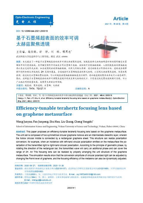
DOI: 10.12086/oee.2021.200319基于石墨烯超表面的效率可调太赫兹聚焦透镜王俊瑶,樊俊鹏,舒 好,刘 畅,程用志*武汉科技大学信息科学与工程学院,湖北 武汉 430081摘要:本文提出了一种基于石墨烯超表面的效率可调太赫兹聚焦透镜。
该超表面单元结构由两层对称的圆形镂空石墨烯和中间介质层组成,其中镂空圆形中间由长方形石墨烯片连接。
该结构可实现偏振转换,入射到超表面的圆偏振波将以其正交的形式出射,如左旋圆到右旋圆偏振转换。
利用几何相位原理,通过旋转长方形条的方向,透射波会携带额外的附加相位并能满足2π范围内覆盖。
合适地排列石墨烯超表面的单元结构,以实现太赫兹聚焦透镜。
仿真结果表明:通过改变石墨烯的费米能级,可以对超表面圆偏振转换幅度进行调节,进而超透镜的聚焦效率也可以动态调节。
因此,这种基于石墨烯超表面的效率可调聚焦透镜不用改变单元结构的尺寸,只需通过改变费米能级便可实现,可以广泛地应用到能量收集、成像等太赫兹应用领域。
关键词:超表面;聚焦透镜;石墨烯;太赫兹中图分类号:TH74;TQ127.11 文献标志码:A王俊瑶,樊俊鹏,舒好,等. 基于石墨烯超表面的效率可调太赫兹聚焦透镜[J]. 光电工程,2021,48(4): 200319Wang J Y , Fan J P , Shu H, et al. Efficiency-tunable terahertz focusing lens based on graphene metasurface[J]. Opto-Electron Eng , 2021, 48(4): 200319Efficiency-tunable terahertz focusing lens based on graphene metasurfaceWang Junyao, Fan Junpeng, Shu Hao, Liu Chang, Cheng Yongzhi *School of Information Science and Engineering, Wuhan University of Science and Technology, Wuhan, Hubei 430081, China Abstract: This paper proposes an efficiency-tunable terahertz focusing lens based on the graphene metasurface. The unit cell is composed of two symmetrical circular graphene hollows and an intermediate dielectric layer, wherein the hollow circular middle is connected by a rectangular graphene sheet. This structure can realize polarization conversion, for example, when an incidence with left-hand circular polarization emitted on the metasurface the po-larization of the transmitted light is right-hand circular polarization. According to the principle of geometric phase, by rotating the direction of the rectangular bar, the transmitted wave will carry an additional phase and can cover the range of 2π. An THz focusing lens can be realized by properly arranging the unit structure of the graphene metasurface. The simulation results show that the conversion amplitude of circular polarized light can be adjusted by changing the Fermi level of graphene, and the focusing efficiency of the metalens can also be dynamically adjusted.LCPRCP(cross-polarization)xy zV g——————————————————收稿日期:2020-08-27; 收到修改稿日期:2020-10-26基金项目:湖北省教育厅科技研究计划重点项目(D2*******);武汉科技大学研究生创新基金项目(JCX201959);大学生创新基金项目资助课题(20ZA083)作者简介:王俊瑶(2000-),女,主要从事电子科学与技术专业。
高功率平板波导螺旋阵列天线设计
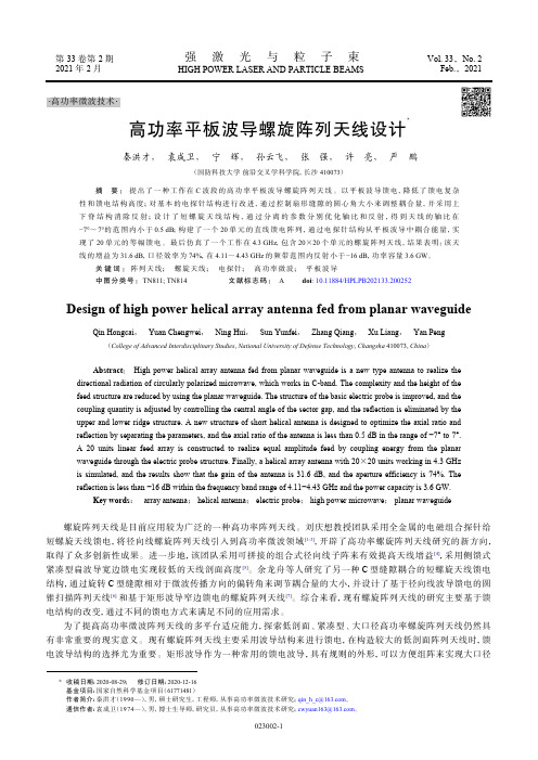
·高功率微波技术·高功率平板波导螺旋阵列天线设计*秦洪才, 袁成卫, 宁 辉, 孙云飞, 张 强, 许 亮, 严 鹏(国防科技大学 前沿交叉学科学院,长沙 410073)摘 要: 提出了一种工作在C 波段的高功率平板波导螺旋阵列天线。
以平板波导馈电,降低了馈电复杂性和馈电结构高度;对基本的电探针结构进行改进,通过控制扇形缝隙的圆心角大小来调整耦合量,并采用上下脊结构消除反射;设计了短螺旋天线结构,通过分离的参数分别优化轴比和反射,得到天线的轴比在−7°~7°的范围内小于0.5 dB ;构建了一个20单元的直线馈电阵列,通过电探针结构从平板波导中耦合能量,实现了20单元的等幅馈电。
最后仿真了一个工作在4.3 GHz ,包含20×20个单元的螺旋阵列天线,结果表明:该天线的增益为31.6 dB ,口径效率为74%,在4.11~4.43 GHz 的频带范围内反射小于−16 dB ,功率容量3.6 GW 。
关键词: 阵列天线; 螺旋天线; 电探针; 高功率微波; 平板波导中图分类号: TN811; TN814 文献标志码: A doi : 10.11884/HPLPB202133.200252Design of high power helical array antenna fed from planar waveguideQin Hongcai , Yuan Chengwei , Ning Hui , Sun Yunfei , Zhang Qiang , Xu Liang , Yan Peng(College of Advanced Interdisciplinary Studies , National University of Defense Technology , Changsha 410073, China )Abstract : High power helical array antenna fed from planar waveguide is a new type antenna to realize the directional radiation of circularly polarized microwave, which works in C-band. The complexity and the height of the feed structure are reduced by using the planar waveguide. The structure of the basic electric probe is improved, and the coupling quantity is adjusted by controlling the central angle of the sector gap, and the reflection is eliminated by the upper and lower ridge structure. A new structure of short helical antenna is designed to optimize the axial ratio and reflection by separating the parameters, and the axial ratio of the antenna is less than 0.5 dB in the range of −7° to 7°.A 20 units linear feed array is constructed to realize equal amplitude feed by coupling energy from the planar waveguide through the electric probe structure. Finally, a helical array antenna with 20×20 units working in 4.3 GHz is simulated, and the results show that the gain of the antenna is 31.6 dB, and the aperture efficiency is 74%. The reflection is less than −16 dB within the frequency band range of 4.11−4.43 GHz and the power capacity is 3.6 GW.Key words : array antenna ; helical antenna ; electric probe ; high power microwave ; planar waveguide螺旋阵列天线是目前应用较为广泛的一种高功率阵列天线。
斯仑贝谢所有测井曲线英文名称解释

斯仑贝谢所有测井曲线英文名称解释OCEAN DRILLING PROGRAMACRONYMS USED FOR WIRELINE SCHLUMBERGER TOOLS ACT Aluminum Clay ToolAMS Auxiliary Measurement SondeAPS Accelerator Porosity SondeARI Azimuthal Resistivity ImagerASI Array Sonic ImagerBGKT Vertical Seismic Profile ToolBHC Borehole Compensated Sonic ToolBHTV Borehole TeleviewerCBL Casing Bond LogCNT Compensated Neutron ToolDIT Dual Induction ToolDLL Dual LaterologDSI Dipole Sonic ImagerFMS Formation MicroScannerGHMT Geologic High Resolution Magnetic ToolGPIT General Purpose Inclinometer ToolGR Natural Gamma RayGST Induced Gamma Ray Spectrometry ToolHLDS Hostile Environment Lithodensity SondeHLDT Hostile Environment Lithodensity ToolHNGS Hostile Environment Gamma Ray SondeLDT Lithodensity ToolLSS Long Spacing Sonic ToolMCD Mechanical Caliper DeviceNGT Natural Gamma Ray Spectrometry ToolNMRT Nuclear Resonance Magnetic ToolQSST Inline Checkshot ToolSDT Digital Sonic ToolSGT Scintillation Gamma Ray ToolSUMT Susceptibility Magnetic ToolUBI Ultrasonic Borehole ImagerVSI Vertical Seismic ImagerWST Well Seismic ToolWST-3 3-Components Well Seismic ToolOCEAN DRILLING PROGRAMACRONYMS USED FOR LWD SCHLUMBERGER TOOLSADN Azimuthal Density-NeutronCDN Compensated Density-NeutronCDR Compensated Dual ResistivityISONIC Ideal Sonic-While-DrillingNMR Nuclear Magnetic ResonanceRAB Resistivity-at-the-BitOCEAN DRILLING PROGRAMACRONYMS USED FOR NON-SCHLUMBERGER SPECIALTY TOOLSMCS Multichannel Sonic ToolMGT Multisensor Gamma ToolSST Shear Sonic ToolTAP Temperature-Acceleration-Pressure ToolTLT Temperature Logging ToolOCEAN DRILLING PROGRAMACRONYMS AND UNITS USED FOR WIRELINE SCHLUMBERGER LOGSAFEC APS Far Detector Counts (cps)ANEC APS Near Detector Counts (cps)AX Acceleration X Axis (ft/s2)AY Acceleration Y Axis (ft/s2)AZ Acceleration Z Axis (ft/s2)AZIM Constant Azimuth for Deviation Correction (deg)APLC APS Near/Array Limestone Porosity Corrected (%)C1 FMS Caliper 1 (in)C2 FMS Caliper 2 (in)CALI Caliper (in)CFEC Corrected Far Epithermal Counts (cps)CFTC Corrected Far Thermal Counts (cps)CGR Computed (Th+K) Gamma Ray (API units)CHR2 Peak Coherence, Receiver Array, Upper DipoleCHRP Compressional Peak Coherence, Receiver Array, P&SCHRS Shear Peak Coherence, Receiver Array, P&SCHTP Compressional Peak Coherence, Transmitter Array, P&SCHTS Shear Peak Coherence, Transmitter Array, P&SCNEC Corrected Near Epithermal Counts (cps)CNTC Corrected Near Thermal Counts (cps)CS Cable Speed (m/hr)CVEL Compressional Velocity (km/s)DATN Discriminated Attenuation (db/m)DBI Discriminated Bond IndexDEVI Hole Deviation (degrees)DF Drilling Force (lbf)DIFF Difference Between MEAN and MEDIAN in Delta-Time Proc. (microsec/ft) DRH HLDS Bulk Density Correction (g/cm3)DRHO Bulk Density Correction (g/cm3)DT Short Spacing Delta-Time (10'-8' spacing; microsec/ft)DT1 Delta-Time Shear, Lower Dipole (microsec/ft)DT2 Delta-Time Shear, Upper Dipole (microsec/ft)DT4P Delta- Time Compressional, P&S (microsec/ft)DT4S Delta- Time Shear, P&S (microsec/ft))DT1R Delta- Time Shear, Receiver Array, Lower Dipole (microsec/ft)DT2R Delta- Time Shear, Receiver Array, Upper Dipole (microsec/ft)DT1T Delta-Time Shear, Transmitter Array, Lower Dipole (microsec/ft)DT2T Delta-Time Shear, Transmitter Array, Upper Dipole (microsec/ft)DTCO Delta- Time Compressional (microsec/ft)DTL Long Spacing Delta-Time (12'-10' spacing; microsec/ft)DTLF Long Spacing Delta-Time (12'-10' spacing; microsec/ft)DTLN Short Spacing Delta-Time (10'-8' spacing; microsec/ftDTRP Delta-Time Compressional, Receiver Array, P&S (microsec/ft)DTRS Delta-Time Shear, Receiver Array, P&S (microsec/ft)DTSM Delta-Time Shear (microsec/ft)DTST Delta-Time Stoneley (microsec/ft)DTTP Delta-Time Compressional, Transmitter Array, P&S (microsec/ft)DTTS Delta-Time Shear, Transmitter Array, P&S (microsec/ft)ECGR Environmentally Corrected Gamma Ray (API units)EHGR Environmentally Corrected High Resolution Gamma Ray (API units) ENPH Epithermal Neutron Porosity (%)ENRA Epithermal Neutron RatioETIM Elapsed Time (sec)FINC Magnetic Field Inclination (degrees)FNOR Magnetic Field Total Moment (oersted)FX Magnetic Field on X Axis (oersted)FY Magnetic Field on Y Axis (oersted)FZ Magnetic Field on Z Axis (oersted)GR Natural Gamma Ray (API units)HALC High Res. Near/Array Limestone Porosity Corrected (%)HAZI Hole Azimuth (degrees)HBDC High Res. Bulk Density Correction (g/cm3)HBHK HNGS Borehole Potassium (%)HCFT High Resolution Corrected Far Thermal Counts (cps)HCGR HNGS Computed Gamma Ray (API units)HCNT High Resolution Corrected Near Thermal Counts (cps)HDEB High Res. Enhanced Bulk Density (g/cm3)HDRH High Resolution Density Correction (g/cm3)HFEC High Res. Far Detector Counts (cps)HFK HNGS Formation Potassium (%)HFLC High Res. Near/Far Limestone Porosity Corrected (%)HEGR Environmentally Corrected High Resolution Natural Gamma Ray (API units) HGR High Resolution Natural Gamma Ray (API units)HLCA High Res. Caliper (inHLEF High Res. Long-spaced Photoelectric Effect (barns/e-)HNEC High Res. Near Detector Counts (cps)HNPO High Resolution Enhanced Thermal Nutron Porosity (%)HNRH High Resolution Bulk Density (g/cm3)HPEF High Resolution Photoelectric Effect (barns/e-)HRHO High Resolution Bulk Density (g/cm3)HROM High Res. Corrected Bulk Density (g/cm3)HSGR HNGS Standard (total) Gamma Ray (API units)HSIG High Res. Formation Capture Cross Section (capture units) HSTO High Res. Computed Standoff (in)HTHO HNGS Thorium (ppm)HTNP High Resolution Thermal Neutron Porosity (%)HURA HNGS Uranium (ppm)IDPH Phasor Deep Induction (ohmm)IIR Iron Indicator Ratio [CFE/(CCA+CSI)]ILD Deep Resistivity (ohmm)ILM Medium Resistivity (ohmm)IMPH Phasor Medium Induction (ohmm)ITT Integrated Transit Time (s)LCAL HLDS Caliper (in)LIR Lithology Indicator Ratio [CSI/(CCA+CSI)]LLD Laterolog Deep (ohmm)LLS Laterolog Shallow (ohmm)LTT1 Transit Time (10'; microsec)LTT2 Transit Time (8'; microsec)LTT3 Transit Time (12'; microsec)LTT4 Transit Time (10'; microsec)MAGB Earth's Magnetic Field (nTes)MAGC Earth Conductivity (ppm)MAGS Magnetic Susceptibility (ppm)MEDIAN Median Delta-T Recomputed (microsec/ft)MEAN Mean Delta-T Recomputed (microsec/ft)NATN Near Pseudo-Attenuation (db/m)NMST Magnetometer Temperature (degC)NMSV Magnetometer Signal Level (V)NPHI Neutron Porosity (%)NRHB LDS Bulk Density (g/cm3)P1AZ Pad 1 Azimuth (degrees)PEF Photoelectric Effect (barns/e-)PEFL LDS Long-spaced Photoelectric Effect (barns/e-)PIR Porosity Indicator Ratio [CHY/(CCA+CSI)]POTA Potassium (%)RB Pad 1 Relative Bearing (degrees)RHL LDS Long-spaced Bulk Density (g/cm3)RHOB Bulk Density (g/cm3)RHOM HLDS Corrected Bulk Density (g/cm3)RMGS Low Resolution Susceptibility (ppm)SFLU Spherically Focused Log (ohmm)SGR Total Gamma Ray (API units)SIGF APS Formation Capture Cross Section (capture units)SP Spontaneous Potential (mV)STOF APS Computed Standoff (in)SURT Receiver Coil Temperature (degC)SVEL Shear Velocity (km/s)SXRT NMRS differential Temperature (degC)TENS Tension (lb)THOR Thorium (ppm)TNRA Thermal Neutron RatioTT1 Transit Time (10' spacing; microsec)TT2 Transit Time (8' spacing; microsec)TT3 Transit Time (12' spacing; microsec)TT4 Transit Time (10' spacing; microsec)URAN Uranium (ppm)V4P Compressional Velocity, from DT4P (P&S; km/s)V4S Shear Velocity, from DT4S (P&S; km/s)VELP Compressional Velocity (processed from waveforms; km/s)VELS Shear Velocity (processed from waveforms; km/s)VP1 Compressional Velocity, from DT, DTLN, or MEAN (km/s)VP2 Compressional Velocity, from DTL, DTLF, or MEDIAN (km/s)VCO Compressional Velocity, from DTCO (km/s)VS Shear Velocity, from DTSM (km/s)VST Stonely Velocity, from DTST km/s)VS1 Shear Velocity, from DT1 (Lower Dipole; km/s)VS2 Shear Velocity, from DT2 (Upper Dipole; km/s)VRP Compressional Velocity, from DTRP (Receiver Array, P&S; km/s) VRS Shear Velocity, from DTRS (Receiver Array, P&S; km/s)VS1R Shear Velocity, from DT1R (Receiver Array, Lower Dipole; km/s) VS2R Shear Velocity, from DT2R (Receiver Array, Upper Dipole; km/s) VS1T Shear Velocity, from DT1T (Transmitter Array, Lower Dipole; km/s) VS2T Shear Velocity, from DT2T (Transmitter Array, Upper Dipole; km/s) VTP Compressional Velocity, from DTTP (Transmitter Array, P&S; km/s) VTS Shear Velocity, from DTTS (Transmitter Array, P&S; km/s)#POINTS Number of Transmitter-Receiver Pairs Used in Sonic Processing W1NG NGT Window 1 counts (cps)W2NG NGT Window 2 counts (cps)W3NG NGT Window 3 counts (cps)W4NG NGT Window 4 counts (cps)W5NG NGT Window 5 counts (cps)OCEAN DRILLING PROGRAMACRONYMS AND UNITS USED FOR LWD SCHLUMBERGER LOGSAT1F Attenuation Resistivity (1 ft resolution; ohmm)AT3F Attenuation Resistivity (3 ft resolution; ohmm)AT4F Attenuation Resistivity (4 ft resolution; ohmm)AT5F Attenuation Resistivity (5 ft resolution; ohmm)ATR Attenuation Resistivity (deep; ohmm)BFV Bound Fluid Volume (%)B1TM RAB Shallow Resistivity Time after Bit (s)B2TM RAB Medium Resistivity Time after Bit (s)B3TM RAB Deep Resistivity Time after Bit (s)BDAV Deep Resistivity Average (ohmm)BMAV Medium Resistivity Average (ohmm)BSAV Shallow Resistivity Average (ohmm)CGR Computed (Th+K) Gamma Ray (API units)DCAL Differential Caliper (in)DROR Correction for CDN rotational density (g/cm3).DRRT Correction for ADN rotational density (g/cm3).DTAB AND or CDN Density Time after Bit (hr)FFV Free Fluid Volume (%)GR Gamma Ray (API Units)GR7 Sum Gamma Ray Windows GRW7+GRW8+GRW9-Equivalent to Wireline NGT window 5 (cps) GRW3 Gamma Ray Window 3 counts (cps)-Equivalent to Wireline NGT window 1GRW4 Gamma Ray Window 4 counts (cps)-Equivalent to Wireline NGT window 2GRW5 Gamma Ray Window 5 counts (cps)-Equivalent to Wireline NGT window 3GRW6 Gamma Ray Window 6 counts (cps)-Equivalent to Wireline NGT window 4GRW7 Gamma Ray Window 7 counts (cps)GRW8 Gamma Ray Window 8 counts (cps)GRW9 Gamma Ray Window 9 counts (cps)GTIM CDR Gamma Ray Time after Bit (s)GRTK RAB Gamma Ray Time after Bit (s)HEF1 Far He Bank 1 counts (cps)HEF2 Far He Bank 2 counts (cps)HEF3 Far He Bank 3 counts (cps)HEF4 Far He Bank 4 counts (cps)HEN1 Near He Bank 1 counts (cps)HEN2 Near He Bank 2 counts (cps)HEN3 Near He Bank 3 counts (cps)HEN4 Near He Bank 4 counts (cps)MRP Magnetic Resonance PorosityNTAB ADN or CDN Neutron Time after Bit (hr)PEF Photoelectric Effect (barns/e-)POTA Potassium (%) ROPE Rate of Penetration (ft/hr)PS1F Phase Shift Resistivity (1 ft resolution; ohmm)PS2F Phase Shift Resistivity (2 ft resolution; ohmm)PS3F Phase Shift Resistivity (3 ft resolution; ohmm)PS5F Phase Shift Resistivity (5 ft resolution; ohmm)PSR Phase Shift Resistivity (shallow; ohmm)RBIT Bit Resistivity (ohmm)RBTM RAB Resistivity Time After Bit (s)RING Ring Resistivity (ohmm)ROMT Max. Density Total (g/cm3) from rotational processing ROP Rate of Penetration (m/hr)ROP1 Rate of Penetration, average over last 1 ft (m/hr).ROP5 Rate of Penetration, average over last 5 ft (m/hr)ROPE Rate of Penetration, averaged over last 5 ft (ft/hr)RPM RAB Tool Rotation Speed (rpm)RTIM CDR or RAB Resistivity Time after Bit (hr)SGR Total Gamma Ray (API units)T2 T2 Distribution (%)T2LM T2 Logarithmic Mean (ms)THOR Thorium (ppm)TNPH Thermal Neutron Porosity (%)TNRA Thermal RatioURAN Uranium (ppm)OCEAN DRILLING PROGRAMADDITIONAL ACRONYMS AND UNITS(PROCESSED LOGS FROM GEOCHEMICAL TOOL STRING)AL2O3 Computed Al2O3 (dry weight %)AL2O3MIN Computed Al2O3 Standard Deviation (dry weight %) AL2O3MAX Computed Al2O3 Standard Deviation (dry weight %) CAO Computed CaO (dry weight %)CAOMIN Computed CaO Standard Deviation (dry weight %) CAOMAX Computed CaO Standard Deviation (dry weight %) CACO3 Computed CaCO3 (dry weight %)CACO3MIN Computed CaCO3 Standard Deviation (dry weight %) CACO3MAX Computed CaCO3 Standard Deviation (dry weight %) CCA Calcium Yield (decimal fraction)CCHL Chlorine Yield (decimal fraction)CFE Iron Yield (decimal fraction)CGD Gadolinium Yield (decimal fraction)CHY Hydrogen Yield (decimal fraction)CK Potassium Yield (decimal fraction)CSI Silicon Yield (decimal fraction)CSIG Capture Cross Section (capture units)CSUL Sulfur Yield (decimal fraction)CTB Background Yield (decimal fraction)CTI Titanium Yield (decimal fraction)FACT Quality Control CurveFEO Computed FeO (dry weight %)FEOMIN Computed FeO Standard Deviation (dry weight %) FEOMAX Computed FeO Standard Deviation (dry weight %) FEO* Computed FeO* (dry weight %)FEO*MIN Computed FeO* Standard Deviation (dry weight %) FEO*MAX Computed FeO* Standard Deviation (dry weight %) FE2O3 Computed Fe2O3 (dry weight %)FE2O3MIN Computed Fe2O3 Standard Deviation (dry weight %) FE2O3MAX Computed Fe2O3 Standard Deviation (dry weight %) GD Computed Gadolinium (dry weight %)GDMIN Computed Gadolinium Standard Deviation (dry weight %) GDMAX Computed Gadolinium Standard Deviation (dry weight %) K2O Computed K2O (dry weight %)K2OMIN Computed K2O Standard Deviation (dry weight %)K2OMAX Computed K2O Standard Deviation (dry weight %) MGO Computed MgO (dry weight %)MGOMIN Computed MgO Standard Deviation (dry weight %) MGOMAX Computed MgO Standard Deviation (dry weight %)S Computed Sulfur (dry weight %)SMIN Computed Sulfur Standard Deviation (dry weight %) SMAX Computed Sulfur Standard Deviation (dry weight %)SIO2 Computed SiO2 (dry weight %)SIO2MIN Computed SiO2 Standard Deviation (dry weight %) SIO2MAX Computed SiO2 Standard Deviation (dry weight %) THORMIN Computed Thorium Standard Deviation (ppm) THORMAX Computed Thorium Standard Deviation (ppm)TIO2 Computed TiO2 (dry weight %)TIO2MIN Computed TiO2 Standard Deviation (dry weight %) TIO2MAX Computed TiO2 Standard Deviation (dry weight %) URANMIN Computed Uranium Standard Deviation (ppm) URANMAX Computed Uranium Standard Deviation (ppm) VARCA Variable CaCO3/CaO calcium carbonate/oxide factor。
铁电超晶格(薄膜)简介

例如:SrTiO3,LaAlO3,SrRuO3……
6
Granzon等设计一个试验方法研究 PZT陶瓷在应力下得极化和压电性质
BST
BST
7
BST
BST
泊松比V=0.48
8
基于DFT的第一性原理研究模型:
假设: 1. 在零应力下BST超晶格被认为是理想的双层钙钛矿结构 2. 电子之间的交换关联式应用LDA 3. 在施加应力时,原子在空间群P4mm里沿[100]方向优化
3
MBE,PLD,ALD
产品广泛应用于太阳能光电、 微电子、光电子、MEMS(微 机电系统)、传感器、半导体 发光照明工程等领域
4
为什么研究铁电体超晶格
实现光子的调控 BaTiO3
压电热点电光…… 材料
热电探测器 薄膜电容器 非易失MRAM 表面声波元件……
5
计算的前期工作
张应力
超晶格
衬底
压应力
single-crystalline BTO is tetragonal a=b=3.994 Å, c=4.033 Å
CTO is orthorhombic a=5.442 Å, b=5.380 Å, c=7.640 Å, and pseudocubic a=c=3.826 Å
APPLIED PHYSICS LETTERS 94, 232904 2009
Born有效电荷1
体系总能
原子i沿着笛卡尔坐标α方向的位移 原子沿笛卡尔坐标β方向的电场
1.Stefano B ,Stefano D G,Andrea D C 2001 Rev.Βιβλιοθήκη Mod. Phys . 73 515
11
The alternation of compressive and tensile strains, which are induced in BTO and CTO layers by STO (cubic, a=3.905 Å )substrates,respectively, can effectively
中国科大纳米多孔V2O5电极材料研究取得新成果
f n e t 1 ,4 12 1 ),以及 证 明了纳米 光学逻 辑 Na o L t . l 7 ( 0 】 1
此 前 ,该研 究小组 与 中国科大 9 1 校友 、加州 大学 河 22
单 元的 片上可集 成性 [ t C mmu Na . o n.2,3 7 d i 1 滨分 校殷 亚 东教 授课题 组 合作 设计 制备 了具 有多 孔结 构 的 8 o : 0.
月 2 日在线 发表 在 Sma 1( 0 1 DOI l 1 0 : 2/S 1 属 纳米 线手 性表 面等 离激 元 可用 于设计 宽带 可调 的 纳米 圆 0. 0 ml .
2 l0 8 8 上 。 0 l0 3 )
偏 振光光 源 ,即纳 米尺度 的 1 /4波 片 ,可用于在 纳 米尺度
这一 特性 为光学 芯片 的高 密度集 成奠 定 了理 论基 础 。
该 研究 小组 在前 期研 究工作 的基 础上 ,采用静 电喷雾
O亚 近年 来 ,中科 院物理研 究所 /北 京凝 聚态物理 国家实 沉 积装置 合成 了一种 由三维多 孔 V, 微米球 构成 的钒 氧
验室 ( ) 红 星研 究组 围绕基于 金属纳 米线 的集成纳 米光 化 物 薄膜材 料 。该 薄膜 材料 作为 正极 材料 应用 于锂 离子 电 筹 徐
研 究 员课题 组在 稀 土掺杂 半导 体 纳米 晶研 究方 面取 得新 进 螺旋地 向前传 播 。 圆偏振 光的产生 原理类 似 , 与 手性 表面等
展 。 研究小 组采用一 种巧 妙的技 术路线 , 该 成功实 现 了稀 土 离激 元也是 由两个具 有 固定 丌 / 相位差 且相 互正交 的分量 2
0 (2 ,4 6 2 0 )、基于纳 米线 网络构筑 的全光路 由器和 均 为 6分 钟 )下 ,电 池 在 2 0次 充放 电循 环 后 仍 能 稳 定 放 出 1 ) 1 8(0 9 ] m 1 g 信号 分离器 [ n et 0 5 , l 5 (0 o1 逻辑 回路 1 0 Ah 的 容 量 。 Na o L t .1 ( ) 9 0 2 l ) 及
基于二氧化钒的可调双宽带太赫兹超材料吸收器

第50卷第4期2023年北京化工大学学报(自然科学版)Journal of Beijing University of Chemical Technology (Natural Science)Vol.50,No.42023引用格式:许中璞,赵永鹏.基于二氧化钒的可调双宽带太赫兹超材料吸收器[J].北京化工大学学报(自然科学版),2023,50(4):107-112.XU ZhongPu,ZHAO YongPeng.A tunable dual broadband terahertz metamaterial absorber based on vanadium dioxide[J].Journal of Beijing University of Chemical Technology (Natural Science),2023,50(4):107-112.基于二氧化钒的可调双宽带太赫兹超材料吸收器许中璞1 赵永鹏2*(1.武威职业学院信息技术学院,武威 733000;2.四川农业大学机电学院,雅安 625000)摘 要:基于VO 2的相变特性提出一种具有双宽带特性的太赫兹超材料吸收器,包括对角放置的VO 2图案层㊁电介质层以及金反射层共3层结构㊂对吸收器的结构建模㊁吸收效果及吸收特性等进行了仿真分析,仿真结果表明,所设计吸收器吸收率大于90%的两个带宽分别为0.73THz 和0.6THz㊂在通过热控制诱导VO 2从绝缘态到金属态的相变过程中,吸收率分别在31%~93.1%和30%~95.2%之间实现连续可调㊂另外,通过研究不同偏振角及入射角下所设计超材料吸收器的吸收性能发现,该吸收器具有偏振无关㊁偏振不敏感以及大入射角吸收特性㊂所设计吸收器有望在如太赫兹通信㊁成像和探测器等利用太赫兹波段领域得到广泛应用㊂关键词:VO 2相变特性;超材料;太赫兹吸收器;连续可调中图分类号:O436 DOI :10.13543/j.bhxbzr.2023.04.014收稿日期:2023-02-13基金项目:四川省自然科学基金(2023NSFSC0435)第一作者:男,1988年生,硕士*通信联系人E⁃mail:zhaoyp@引 言太赫兹波的工作频率在0.1~10THz,相应的波长在0.03~3mm [1]㊂大多数天然材料在太赫兹频率下表现出微弱的电磁响应,这种现象被称为 太赫兹间隙”㊂而超材料是一种人工设计的周期性结构材料,具有天然材料所不具备的超常物理属性,其奇异的光学特性由所设计的人工周期性结构决定[2]㊂基于超材料的电磁特性,有学者研究了其在操纵太赫兹辐射方面的实用性[3]㊂太赫兹吸收器是太赫兹领域最具吸引力的研究课题之一,由于其在探测㊁成像和调制方面的重要应用前景,受到了人们的广泛关注㊂随着超材料这一概念的引入,太赫兹超材料吸收器得到快速发展㊂在太赫兹波段,关于吸收器已有了大量研究,如超宽带吸收器[4-5]㊁宽带吸收器[6-8]以及窄带吸收器[9-11]等㊂然而,上述绝大多数的吸收器存在一个功能上的限制,即大多数吸收器的电磁波吸收率是不可以调节的,一旦设计完成,其功能就己经固定了㊂因此为了面对日益复杂的电磁应用环境,需要设计一种吸收率可调节的超材料吸收器㊂要实现吸收器的吸收率可调,主要手段是在超材料结构中引入活性材料(如相变材料㊁石墨烯等),使其主动控制超材料吸收器的光学特性㊂二氧化钒(VO 2)是控制器件的理想选择,当施加热㊁外部电场或光学刺激时,可诱导VO 2发生从绝缘态到金属态的可逆相变[12],相变过程中伴随着电导率发生改变,从而实现超材料吸收器的吸收率可调㊂近年来,针对宽带可调太赫兹超材料吸收器已有不少研究,如张婷等[13]基于VO 2设计了一种90%以上吸收带宽为1.06THz 以及吸收率在4%~99.5%之间可调的超材料吸收器;Wang 等[14]基于VO 2设计了一种90%以上的吸收带宽为0.65THz 且吸收率在30%~98%的可调吸收器;Song 等[15]基于VO 2设计了一种90%以上吸收带宽为0.33THz 且吸收率在30%~100%的可调吸收器;Huang 等[16]基于VO 2设计了一种80%以上吸收带宽分别为0.88THz 和0.77THz 且吸收率在20%~90%的可调双宽带吸收器;刘苏雅拉图[17]提出一种二氧化钒开口环阵列组成的宽带可调谐吸收器;晋豪[18]提出一种表面由石墨烯圆盘构成的 葫芦形”图案的超材料吸收器;樊怡等[19]提出基于VO 2相变特性的温度可调控双频太赫兹超材料吸收器;马燕燕[20]提出了一种双频可调谐㊁双频可切换㊁宽带可切换的超材料吸收器;王佳云[21]设计了一种极化可控的单频/五频段超材料吸收器;杨森等[22]设计出一种基于光激发动态可切换的超材料吸收器㊂基于以上分析,目前对于超材料吸收器的研究主要集中在拓宽工作带宽㊁实现宽带可调谐以及提高吸收率和吸收性能等方面㊂为了进一步拓宽工作带宽和提高可调谐范围,本文提出一种基于VO 2的双宽带太赫兹超材料吸收器,其由两个相同的VO 2图案在经典的金属-电介质-金属结构的顶部对角排列而成㊂通过在热控制下诱导VO 2发生从绝缘态到金属态的相变,可以连续调节两个频段的吸收率㊂该吸收器具有偏振无关㊁偏振不敏感以及大入射角吸收特性,在太赫兹波段具有广泛的应用前景,如太赫兹通信㊁成像和探测器等㊂图1 双宽带太赫兹超材料吸收器单元结构示意图Fig.1 Schematic view of the dual broadband terahertzmetamaterial absorber structure1 太赫兹超材料吸收器的结构设计本文提出的双宽带太赫兹超材料单元结构示意图如图1所示㊂该结构包括3层,从上到下依次为对角放置的VO 2图案层㊁电介质层和底部金反射层,其中金的电导率为4.56×10⁷S /m[23],SiO 2的相对介电常数为3.9+0.03i [16]㊂最优结构参数取值如下:单元结构周期P =180μm,金反射层厚度h 1=0.2μm,SiO 2电介质层厚度h 2=36μm,VO 2图案层厚度t =0.1μm,VO 2图案到周期边界的间隙g =11μm,对角图案开口宽度w =23μm,对角图案开口长度l =110μm㊂本文使用CST MICROWAVE STU⁃DIO 软件,通过有限元方法进行全波电磁仿真,在仿真过程中采用频域求解器,使用四面体自适应网格剖分㊂在x 和y 方向采用unit cell 边界条件,在z 方向采用open(add space)边界条件㊂图2 VO 2介电常数随电导率的变化Fig.2 Variation of the permittivity of VO 2withconductivity该结构的光学介电常数可由Drude 模型[24]描述ε(ω)=ε∞-ω2p (σ)ω2+i γω(1)式中,ε∞=12为高频介电常数,γ=5.75×10¹³rad /s 为碰撞频率,σ处的等离子体频率ω2p (σ)=σσ0ω2p (σ0),ωp (σ0)=1.4×10¹⁵rad /s,σ0=3×105S /m㊂在热控制下,VO 2可以发生由绝缘态到金属态的可逆相变,其电导率σ可由2×10²S /m 变化到2×10⁵S /m㊂根据式(1),利用Matlab 软件计算了VO 2介电常数随电导率的变化情况,结果如图2所示㊂可以看出,不同电导率下介电常数实部的变化远小于虚部,当电导率取值为2×10²S /m 时,表现为绝缘体特性,当电导率取值为2×10⁵S /m 时,表现为金属特性㊂在仿真过程中,采用Drude 模型对VO 2的电导率进行取值,与Matlab 计算过程一致㊂当通过热刺激使VO 2温度略高于室温时,可以实现从绝缘体到金属的转变,在相变温度点其电导率提高了㊃801㊃北京化工大学学报(自然科学版) 2023年10000倍,晶体结构由单斜相转变为四方相㊂2 太赫兹超材料吸收器的性能分析在本文中,吸收率定义如下[25]:A(ω)=1-R(ω)-T(ω)=1-|S11(ω)|2-|S21(ω)|2,其中A(ω)㊁R(ω)和T(ω)分别表示吸收率㊁反射率和透射率,S11(ω)和S21(ω)分别为反射系数和透射系数㊂由于底部金反射层的厚度远远大于入射电磁波的趋肤深度,使得入射电磁波无法透过该金属薄膜继续传播,因此T(ω)=0㊂吸收器的吸收率可进一步简化为A(ω)=1-R(ω)=1-|S11(ω)|2㊂横电模(TE)和横磁模(TM)两种偏振方式下吸收器的吸收率㊁反射率以及透射率变化情况的仿真结果如图3(a)所示㊂在0.67THz~1.4THz和2.9THz~3.5THz频率范围内,吸收率大于90%的带宽分别为0.73THz和0.6THz,在0.86THz㊁2.93THz以及3.39THz这3个频率点处吸收率接近于1,表示这些点的吸收接近完美吸收㊂另外,从图中可以看出,两种偏振方式下的吸收率㊁反射率以及透射率变化保持高度一致,表明所设计的超材料吸收器具有偏振无关特性㊂两种偏振方式下的透射率为零,表明理论分析与仿真结果一致㊂在TE偏振下吸收谱随偏振角的变化情况如图3(b)所示,可以看出,改变偏振角对吸收器的吸收性能没有任何影响,表明所设计的吸收器具有偏振不敏感特性㊂另外,由于所设计的VO2图案的对称性,TM偏振下的吸收光谱与TE偏振下的吸收光谱是重合的,这里不再赘述㊂通过热控制诱导VO2从绝缘态到金属态的相变过程中,可以连续调节两个频带的吸收率和带宽,如图4所示㊂从图中可以看出,在VO2电导率由2×102S/m变化到2×105S/m过程中,第一个频带(0.67THz~1.4THz)的吸收率可由31%增大到93.1%,第二个频带(2.9THz~3.5THz)的吸收率可由30%增大到95.2%㊂因此,通过控制VO2电导率可以实现吸收器两个带宽的连续可调㊂为了更好地理解吸收器的吸收性能,引入阻抗匹配理论,在正入射下太赫兹波的相对阻抗可描述为[25]Z r=(1+S11(ω))2-S221(ω)(1-S11(ω))2-S221(ω)(2)式中,Z r=Z/Z0,Z和Z0分别为吸收器的有效阻抗图3 双宽带吸收器的反射谱㊁透射谱和吸收谱以及不同偏振角下的吸收光谱图Fig.3 Reflection,transmission and absorption spectra of the dual broadband absorber and the absorption spectrawith different polarization angles图4 吸收器吸收率随电导率变化情况Fig.4 Variation of the absorption with conductivity 和自由空间阻抗㊂当Z r=Z/Z0=1时,吸收器有效阻抗与自由空间阻抗匹配,吸收率最大㊂当相对阻抗的实部为1,虚部为0时,可以实现阻抗匹配㊂图5为不同电导率下相对阻抗实部和虚部的变化㊂可以看出,当VO2电导率为2×105S/m(金属态)㊃901㊃第4期 许中璞等:基于二氧化钒的可调双宽带太赫兹超材料吸收器时,在0.67THz ~1.4THz 和2.9THz ~3.5THz 两个频率范围内,相对阻抗的实部接近于1,虚部接近于0,实现了完美吸收,与理论分析结果一致㊂图5 不同电导率下相对阻抗实部和虚部的变化Fig.5 Variation of real and imaginary parts of the relativeimpedance for different VO 2conductivities进一步研究了TE 和TM 两种偏振方式下不同入射角对吸收器吸收性能的影响,结果如图6所示㊂TE 偏振入射下(图6(a)),对于第一个频带(0.67THz ~1.4THz),当入射角小于60°时,吸收器能够保持良好的吸收性能,对于第二个频带(2.9THz ~3.5THz),当入射角小于20°时,吸收器能够保持良好的吸收性能;入射角继续增大,第一个宽带的吸收率急剧下降,第二个宽带的中心频率出现蓝移现象,且带宽逐渐变窄㊂在TM 偏振下(图6(b)),对于第一个频带(0.67THz ~1.4THz),当入射角小于60°时,吸收器能够保持良好的吸收性能;对于第二个频带(2.9THz ~3.5THz),当入射角小于20°时,吸收器也能够保持良好的吸收性能,入射角进一步增大,两个频带内的吸收率都显著降低㊂本文所设计吸收器与文献中的吸收器性能对比如表1所示㊂可以看出,与双频吸收器相比,本文所设计的双宽带吸收器在工作带宽和吸收率可调范围两个方面的性能都有所提高;与单频吸收器相比,本文部分工作带宽有所拓宽㊂图6 吸收率随入射角的变化Fig.6 Variation of absorption with incident angle 表1 本文设计吸收器与文献中吸收器的性能对比Table 1 Comparison of the performance of the absorberdesigned in this paper with absorbers reported in the literature吸收器来源材料工作带宽/THz吸收率可调范围文献[13]VO 21.06(吸收率>90%)4%~99.5%文献[14]VO 20.65(吸收率>90%)30%~98%文献[15]VO 20.33(吸收率>90%)30%~100%文献[16]VO 20.88和0.77(吸收率>80%)20%~90%本文设计VO 20.73和0.6(吸收率>90%)30%~95.2%3 结论本文提出了一种由对角放置的VO 2图案层㊁介质层以及金反射层组成的双宽带太赫兹超材料吸收器结构,并根据超材料吸收器的吸收机理对吸收器的吸收性能作出分析㊂仿真结果表明,该吸收器吸收率达90%以上的吸收带宽分别为0.73THz 和㊃011㊃北京化工大学学报(自然科学版) 2023年0.6THz㊂当VO2的电导率由2×10²S/m变化到2×105S/m时,两个频带的吸收率分别可在31%~ 93.1%和30%~95.2%之间连续调节㊂根据阻抗匹配理论分析可知,该吸收器具有偏振无关㊁偏振不敏感以及大入射角吸收特性,因此其在太赫兹通信㊁成像和探测器等方面具有广泛的应用前景㊂参考文献:[1] QIAN J J,ZHOU J,ZHU Z,et al.Polarization⁃insensi⁃tive broadband THz absorber based on circular graphenepatches[J].Nanomaterials,2021,11(10):2709. [2] REN Z,CHENG L,HU L,et al.Photoinduced broad⁃band tunable terahertz absorber based on a VO2thin film[J].ACS Applied Materials&Interfaces,2020,12(43):48811-48819.[3] WANG T L,ZHANG Y P,ZHANG H Y,et al.Dual⁃controlled switchable broadband terahertz absorber basedon a graphene⁃vanadium dioxide metamaterial[J].Opti⁃cal Materials Express,2020,10(2):369-386. [4] ZHU J F,MA Z F,SUN W J,et al.Ultra⁃broadbandterahertz metamaterial absorber[J].Applied Physics Let⁃ters,2014,105(2):021102.[5] RI K J,RI C H,RI S Y.Ultra⁃broadband terahertzmetamaterial absorber using a simple design method[J].Optics Communications,2022,515:128191. [6] GRANT J,MA Y,SAHA S,et al.Polarization insensi⁃tive,broadband terahertz metamaterial absorber[J].Op⁃tics Letters,2011,36(17):3476-3478. [7] WEN Y Z,MA W,BAILEY J,et al.Broadband tera⁃hertz metamaterial absorber based on asymmetric resona⁃tors with perfect absorption[J].IEEE Transactions onTerahertz Science and Technology,2015,5(3):406-411.[8] CHENG Y Z,ZOU H J,YANG J J,et al.Dual andbroadband terahertz metamaterial absorber based on acompact resonator structure[J].Optical Materials Ex⁃press,2018,8(10):3104-3114.[9] HU D,MENG T H,WANG H Y,et al.Ultra⁃narrow⁃band terahertz perfect metamaterial absorber for refractiveindex sensing application[J].Results in Physics,2020,19:103567.[10]WANG Y,YUE L S,CUI Z J,et al.Optically tunablesingle narrow band all⁃dielectric terahertz metamaterialsabsorber[J].AIP Advances,2020,10(4):045039.[11]CHEN F,CHENG Y Z,LUO H.Temperature tunablenarrow⁃band terahertz metasurface absorber based on InSbmicro⁃cylinder arrays for enhanced sensing application[J].IEEE Access,2020,8:82981-82988. [12]REN Y,ZHOU T L,JIANG C,et al.Thermally switc⁃hing between perfect absorber and asymmetric transmis⁃sion in vanadium dioxide⁃assisted metamaterials[J].Op⁃tics Express,2021,29(5):7666-7679. [13]张婷,杨森,于新颖.基于二氧化钒的可调宽带太赫兹完美吸收器设计[J].激光与光电子学进展,2021,58(21):250-256.ZHANG T,YANG S,YU X Y.Tunable broadband tera⁃hertz perfect absorber design based on vanadium dioxide[J].Laser and Optoelectronics Progress,2021,58(21):250-256.(in Chinese)[14]WANG S X,CAI C F,YOU M H,et al.Vanadium di⁃oxide based broadband THz metamaterial absorbers withhigh tunability:simulation study[J].Optics Express,2019,27(14):19436-19447.[15]SONG Z Y,WANG K,LI J W,et al.Broadband tunableterahertz absorber based on vanadium dioxide metamateri⁃als[J].Optics Express,2018,26(6):7148-7154.[16]HUANG J,LI J N,YANG Y,et al.Active controllabledual broadband terahertz absorber based on hybrid meta⁃materials with vanadium dioxide[J].Optics Express,2020,28(5):7018-7027.[17]刘苏雅拉图.基于石墨烯和二氧化钒的太赫兹可调谐超材料吸收器[D].呼和浩特:内蒙古大学,2022.LIU S Y.Terahertz tunable metamaterial absorber basedon graphene and vanadium dioxide[D].Hohhot:InnerMongolia University,2022.(in Chinese) [18]晋豪.基于石墨烯圆盘的超材料吸收器的研究[D].成都:四川师范大学,2022.JIN H.Study on metamaterial absorbers based on gra⁃phene disks[D].Chengdu:Sichuan Normal University,2022.(in Chinese)[19]樊怡,杨荣草.基于VO2温度可调控双频超薄太赫兹超材料吸收器[J].量子光学学报,2022,28(1):46-54.FAN Y,YANG R C.Temperature⁃tunable dual⁃band ul⁃tra⁃thin terahertz metamaterial absorber based on vanadi⁃um dioxide[J].Journal of Quantum Optics,2022,28(1):46-54.(in Chinese)[20]马燕燕.双频及宽带可调控超材料吸收器的研究[D].太原:山西大学,2021.MA Y Y.Research on dual⁃band and broadband control⁃lable metamaterial absorbers[D].Taiyuan:Shanxi Uni⁃versity,2021.(in Chinese)[21]王佳云.多频/宽频电磁超材料吸收器和极化转换器的研究[D].太原:山西大学,2021.㊃111㊃第4期 许中璞等:基于二氧化钒的可调双宽带太赫兹超材料吸收器WANG J Y.Study on multi⁃band/broadband absorbersand polarization converters based on electromagneticmetamaterials[D].Taiyuan:Shanxi University,2021.(in Chinese)[22]杨森,袁苏,王佳云.一种光激发可切换的双频太赫兹超材料吸收器[J].光学学报,2021,41(2):0216001.YANG S,YUAN S,WANG J Y.Light⁃excited andswitchable dual⁃band terahertz metamaterial absorber[J].Acta Optica Sinica,2021,41(2):0216001.(inChinese)[23]YAN D X,MENG M,LI J S,et al.Vanadium dioxide⁃assisted broadband absorption and linear⁃to⁃circular polar⁃ization conversion based on a single metasurface designfor the terahertz wave[J].Optics Express,2020,28(20):29843-29854.[24]WANG S X,KANG L,WERNER D H.Hybrid resona⁃tors and highly tunable terahertz metamaterials enabled byvanadium dioxide(VO2)[J].Scientific Reports,2017,7:4326.[25]CHE Z G,LI Z X,ZHANG G M,et al.Active controlla⁃ble broadband absorber based on vanadium dioxide[C]∥2021Photonics&Electromagnetics Research Symposium(PIERS).Hangzhou:IEEE,2021:604-608.A tunable dual broadband terahertz metamaterial absorberbased on vanadium dioxideXU ZhongPu1 ZHAO YongPeng2*(rmation Technology College,Wuwei Vocational College,Wuwei733000;2.College of Mechanical and Electrical Engineering,Sichuan Agricultural University,Ya’an625000,China) Abstract:A terahertz metamaterial absorber with dual broadband characteristics based on the phase transition char⁃acteristics of VO2has been fabricated.The absorber is composed of three layers,a diagonally placed VO2pattern layer,a dielectric layer and a gold reflector.The simulation results show that there are two bandwidths with absorp⁃tivity greater than90%at0.73THz and0.6THz.During the phase transition from the insulating state to the me⁃tallic state of VO2induced by thermal control,the absorption rate is continuously tunable in the range31%-93.1%and30%-95.2%,respectively.In addition,by studying the absorption performance of the metamaterial absorber at different polarization angles and incidence angles,it is found that the absorber has polarization⁃inde⁃pendent,polarization⁃insensitive and large incidence angle absorption characteristics.The absorber has broad pros⁃pects for applications in the terahertz band region,such as in terahertz communication,imaging and detectors. Key words:VO2phase transition property;metamaterial;terahertz absorber;continuously tunable(责任编辑:吴万玲)㊃211㊃北京化工大学学报(自然科学版) 2023年。
一种以空气为基板的圆极化微带天线的设计

一种以空气为基板的圆极化微带天线的设计张昕;杨霭宁;崔闻;曹磊【摘要】An ultra-high frequency circularly polarized(CP)rectangular microstrip antenna on air substrate was designed.The antenna inserted four same slots on the microstrip patch and a small slot on the center of the patch, which could reduce the size of the patch and achieve the circular polarization operation. The impact of antenna parameters on its circularly polarized performance is introduced. Through optimizing the antenna parameters, experimental results show that a good CP radiation performance can be gained.%设计了一种以空气为基板的超高频(UHF)圆极化矩形微带天线.该天线通过在微带贴片四周与中心开槽,减小了天线尺寸,实现天线圆极化的性能.进一步研究了天线的参数对圆极化性能的影响,通过天线参数的优化,使天线达到了良好的圆极化性能.【期刊名称】《现代电子技术》【年(卷),期】2011(034)007【总页数】3页(P104-106)【关键词】微带天线;圆极化;超高频;缝隙天线【作者】张昕;杨霭宁;崔闻;曹磊【作者单位】哈尔滨工程大学信息与通信工程学院,黑龙江哈尔滨,150001;哈尔滨工程大学信息与通信工程学院,黑龙江哈尔滨,150001;哈尔滨工程大学信息与通信工程学院,黑龙江哈尔滨,150001;哈尔滨工程大学信息与通信工程学院,黑龙江哈尔滨,150001【正文语种】中文【中图分类】TN82-340 引言微带天线由于独特的结构和多样化的性能,在各种无线电设备上得到了广泛的应用。
西南大学生物系毕业答辩PPT

理论框架
计算结果与讨论:1.核电荷密度分布 2.核电荷形状因子
西南大学物理科学与技术学院 XXXX级物理学3班 hzx
奇特核电形状因子的研究 毕业论文答辩
程 序 Program
1.利用RCHB方法计算核电荷分布密度 2.在平面波Born近似下计算核电荷形状因子
理论准备充分、扎实; 程序编写仔细、标准; 注意程序中出现的量的单位统一。
result西南大学物理科学与技术学院xxxx级物理学3班hzx奇特核电形状因子的研究li11result西南大学物理科学与技术学院xxxx级物理学3班hzx奇特核电形状因子的研究尽管有相同的质子数但从图中可以清楚的看到的电荷密度分布存在很大的差异由于28s最外面的两个质子束缚很弱导致的电荷密度分布有一个长长的尾巴这清楚的说明在丰质子核28s的基态中存有质子晕
3、远眺开始,双眼看整个图表,产生向前深进的感 觉,然后由外向内逐步辨认每一层的绿白线条。
4、如果视力不良,只能进到某一层时,不要立即停 止远眺,应多看一会儿,将此层看清楚后,再向内 看一层,如此耐心努力争取尽量向内看,才能使眼 的睫状肌放松。
5、双眼视力相近的,两眼可同时远眺;双眼视力相 差大的、将左右眼轮流遮盖,单眼远眺,视力差的 一只眼睛,其远眺时间要延长。
结 果 Result
尽管有相同的质子数,但从 图中可以清楚的看到的电荷密度分 布存在很大的差异,由于28S最外 面的两个质子束缚很弱导致的电荷 密度分布有一个长长的尾巴,这清 楚的说明在丰质子核28S的基态中 存有质子晕。
西南大学物理科学与技术学院 XXXX级物理学3班 hzx
奇特核电形状因子的研究 毕业论文答辩
远眺图使用方法
第一步、首先在能把远眺图都看清的位置,熟悉一 下最远处几个框细微的纹路,
物理专业英语词汇

物理专业英语词汇polarized beam 极化束polarized ion source 极化离子源polarized light 偏振光polarized neutron diffraction technique 极化中子衍射法polarized nucleus 极化核polarized raman scattering 偏振喇曼散射polarized relay 极化继电器polarized target 极化靶polarizer 起偏器偏振器polarizing filter 偏振滤光镜polarizing microscope 偏光显微镜polarizing prism 偏振棱镜polarograph 极谱仪polarography 极谱学polaroid 偏光片polaron 极化子pole 极pole of ecliptic 黄极pole piece 极片pole shoe 极片pole strength 磁极强度polestar 北极星polhode 心迹线polishing 抛光poloidal magnetic field 极向磁场polonium 钋polyatomic molecule 多原子分子polycondensation 缩聚酌polycrystal 多晶polycrystalline material 多晶物质polydisperse system 多色散系polygon of forces 力多边形polygonization 多边形化polymer 聚合物polymer complex 聚合络合物polymer crystal 聚合晶体polymer effect 聚合效应polymerization 聚合polymerization of protein 蛋白质聚合polymolecularity 多分子性polymorphism 多形性polyphase 多相polyphase current 多相电流polytrope 多变性polytropic change 多方状态变化polytropic index 多方指标polytropic process 多变过程pomeranchuk effect 坡密朗丘克效应pomeranchuk theorem 坡密兰丘克定理pomeron 坡密子pool type reactor 池式堆population 全域population inversion 粒子数反转pore 小黑子porosity 多孔性porous flow 多孔流position 位置position resolution 位置分辨率position sensitive detector 对位置灵敏的探测器position vector 位置矢量positive 正片positive charge 正电菏positive column 阳极区positive crystal 正晶体positive electricity 正电positive electrode 阳极positive electron 正电子positive element 正元素positive eyepiece 正目镜positive feedback 正反馈positive hole 空子positive ion 阳离子positive lens 正透镜positive magnetostriction 正磁致伸缩positive meniscus 凹凸透镜positive meson 正介子positive rays 阳射线positon 正电子positron 正电子positron annihilation 正电子湮没positron beam 正电子束positron channeling 正电子沟道positron electron annihilation 偶湮没positron electron tandem ring accelerator 正负电子串列存储环型加速器petra positron emission 正电子发射positron factory 正电子工厂positron spectroscopy 正电子谱学positronium 电子偶素post newtonian approximation 后牛顿近似post nova 燃后新星post post newtonian approximation 后后牛顿近似potassium 钾potassium dihydrogenphosphate 磷酸二氢钾potential 势potential barrier 势垒potential difference 势差potential divider 分压器potential energy 势能potential energy curve 势能曲线potential field 势场potential flow 势流potential function 势函数potential instability 对粱稳定性potential motion 势运动potential scattering 势散射potential well 势阱potentiometer 电位计potts model 波特模型pound 磅powder camera 粉末照相机powder diffraction method 粉末法powder pattern 粉末干涉象powder photography 粉末照相术power 功率power amplification 功率放大power demonstration reactor 动力示范堆power density 功率密度power dissipation 耗散功率power factor 功率因数power factor meter 功率因数计power gain 功率增益power of a lens 透镜的焦强power reactor 动力堆power tube 功率管poynting robertson effect 坡印廷罗伯逊效应poynting's vector 坡印廷矢量practical system of units 实用单位制prandtl number 普朗特数praseodymium 镨pre vacuum 初真空pre vacuum pump 预备真空泵preacceleration 预加速preaccelerator 前加速器preamplifier 前置放大器precession 旋进precession camera 旋进照相机precession of orbit 轨道旋进precessional constant 岁差常数precious metal 贵金属precipitation 沉淀precision 精密度precision measurement 精密测量predict earthquake with catfish 用鲶鱼预报地震prediction 预报prediction of solar activity 太阳活动预告predissociation 预离解preferential recombination 优选复合preionization 预电离preliminary vacuum 初真空pressure 压力pressure broadening 压力增宽pressure coefficient 压力系数pressure dispersion 压力弥散pressure drag 压力阻pressure drop 压降pressure gage 压力表pressure head 压头pressure height equation 气压测高公式pressure of light 光压pressure of water vapor 水汽压pressure sensitive diode 压力敏感二极管pressure sensitive transistor 压力敏感晶体管pressure tensor 压强张量pressurized air 压缩空气pressurized water reactor 压水堆primakoff effect 普里马科夫效应primary battery 原电池primary beam 初级束流原射线束primary cell 原电池primary circuit 原电路primary colors 原色primary cosmic radiation 原宇宙辐射primary cosmic rays 原宇宙射线primary electron 原电子primary energy 一次能量primary ionization 一次电离primary rainbow 昼primary recrystallization 一次再结晶primary standard 原标准primary star 智primary target 初始靶primary thermometer 初始温度计primary voltage 初级电压prime meridian 零子午线prime vertical 卯酉圈primeval galaxy 原始星系primitive black hole 原始黑洞primitive lattice 初基点阵primordial solar nebula 太阳系星云principal axes of stress 应力轴principal axis 轴principal axis of inertia 惯性轴principal index for extraordinary ray 非常光线舟射率principal moment of inertia 知动惯量principal plane 纸面principal point 帚principal quantum number 挚子数principal ray 肘线principal refractive indices 舟射率principal series 诌系principal stress 枝力principle 原理principle of constancy of light velocity 光速不变原理principle of corresponding states 对应态原理principle of detailed balancing 细致平衡原理principle of entropy compensation 熵补偿原理principle of equal a priori probabilities 等验前概率原理principle of equipartition 均分原理principle of equivalence 等价原理principle of equivalence of mass and energy 质能当量原理principle of indeterminancy 测不准原理principle of least action 最小酌原理principle of least constraint 最小约束运动原理principle of microscopic reversibility 微观可逆性原理principle of minimum dissipation of energy 最小能量耗散原理principle of relativity 相对性原理principle of reversibility 可逆性原理principle of superposition 叠加原理principle of virtual displacement 虚位移原理principle of virtual work 虚功原理printed board 印刷电路板printed circuit 印刷电路printer 打印机prism 棱镜prism angle 棱镜角prism spectrograph 棱镜摄谱仪prism spectroscope 棱镜分光镜prismatic transit instrument 折轴中星仪probability 概率probability current density 概率淋度probability density 概率密度probability distribution 概率分布probability distribution function 概率分布函数probability function 概率函数probability of collision 碰撞概率probable error 概率误差probe 探头probe charge 试探电荷probe method 探测法problem of three bodies 三体问题process control 过程控制product nucleus 生成核production 产生production of entropy 熵产生profile drag 翼型阻力profile monitor 剖面监测器prognosis 预报program 程序program library 程序库programme 程序programming language 程序设计语言progressive wave 前进波projecting lens 投影透镜projection 投影projection of crystal 晶体投影projection operator 投影算符projector 投影器幻灯promethium 钷prominence 日珥prominence spectroscope 日珥分光镜prompt neutron 瞬发中子propagation 传播propagation constant 传播常数propagation of sound 声传播propagation velocity 传播速度propagator 传播函数proper channeling 本盏道proper field 固有场proper lorentz group 固有洛伦兹群proper motion 自行proper time 原时proper tone 固有音proper value 本盏proportion 比例proportional component 比例分量proportional counter 正比计数管proportional ionization chamber 正比电离室proportionality factor 比例系数protoatmosphere 原大气protocol 协议proton 质子proton accelerator 质子加速器proton antiproton collision 质子反质子碰撞proton decay 质子衰变proton induced x ray analysis 质子激发x 射线分析proton linear accelerator 质子直线加速器proton number 质子数proton spectrometer 质子谱仪proton synchrotron 质子同步加速器protoplanet 原行星protostar 原恒星protosun 原太阳prototype 原型prototype meter 米原器proximity 附近proximity effect 邻近效应proximity switch 接近开关pseudo crossing 伪交叉pseudo crystal 伪晶体pseudo dipole interaction 伪偶极子相互酌pseudo energy gap 伪能隙pseudo equilibrium 伪平衡pseudo image 假象pseudo plastic flow 伪塑性流pseudo scalar 伪标量pseudo scalar coupling 伪标量耦合pseudo scalar meson 伪标介子pseudo tensor 伪张量pseudo vector 伪矢量pseudo vector coupling 伪矢量耦合pseudo wave 伪波pseudopotential 伪势pseudostate 伪态pseudosymmetry 伪对称pseudovariable 准变星pss method pss 法psychoacoustics 心理声学psychobiophysics 心理生物物理学psychorheology 心理龄学psychrometer 干湿表ptolemaic system 托勒玫体系pulsar 脉冲星pulsating current 脉动电流pulsating star 脉动星pulsating universe 振动宇宙pulsating variable。
基于人工电磁结构的宽带宽波束高增益圆极化微带天线阵

DOI:10.16660/ki.1674-098X.2105-5640-4534基于人工电磁结构的宽带宽波束高增益圆极化微带天线阵林家栋1 柴晋飞2 苏周1 巫勇1(1.空军预警学院 湖北武汉 430019; 2.空军装备部驻成都军事代表局综合处 四川成都 610051)摘 要:圆极化微带天线因其特有的极化优势,在卫星通信系统中有着广泛的应用。
为满足不断发展的卫星通信系统,要求圆极化微带天线具备较宽的带宽和波束。
本文介绍了一型基于人工电磁结构的宽带宽波束高增益圆极化微带天线阵,并进行了仿真,结果表明该天线具有较宽的带宽和波束特性,为圆极化微带天线在卫星通信系统中的应用提供了参考。
关键词:宽带 宽波束 圆极化 微带天线中图分类号:TN823 文献标识码:A 文章编号:1674-098X(2021)05(b)-0128-04Wide-Bandwidth Wide Beam Circular Polarized MicrostripAntenna Array with High Gain Based on ArtificialElectromagnetic StructureLIN Jiadong 1 CHAI Jinfei 2 SU Zhou 1 WU Yong 1(1. Air Force Early Warning Academy, Wuhan, Hubei Province, 430019 China; 2. General Off ice of theMilitary Representative Bureau of the Air Force Equipment Department in Chengdu, Chengdu,Sichuan Province, 610051 China)Abstract : Circularly polarized microstrip antennas are widely used in satellite communication systems due to their unique polarization advantages. In order to meet the ever-developing satellite communication system, the circularly polarized microstrip antenna is required to have a wider bandwidth and beam. A wide-bandwidth wide-beam high-gain circularly polarized microstrip antenna array based on artif icial electromagnetic structure was introduced, and the simulation results show that the antenna has a wide bandwidth and beam characteristic. It provides a reference for the application of the circularly polarized microstrip antenna in the satellite communication system.Key Words : Wide-bandwidth; Wide beam; Circular polarization; Microstrip antenna array作者简介:林家栋(1992—),男,硕士,助教,研究方向为天线。
左_右旋圆极化可重构微带天线_蒲洋

左/右旋圆极化可重构微带天线蒲洋(中国电子科技集团公司第十研究所,成都 610036)摘 要:设计了一种左/右旋圆极化可重构的微带天线。
在矩形微带贴片的两条边上增加枝节,贴片与枝节通过PIN二极管开关连接,通过控制PIN二极管的通断来改变正交模式的相位差,使天线在同一个馈电点上可实现左旋圆极化(LHCP)和右旋圆极化(RHCP)的重构。
该天线在(2800±10)MHz的频率范围内驻波比小于2,轴比小于3dB。
仿真结果与测试结果均验证了该方案的可行性。
关键词:微带天线;圆极化可重构;PIN二极管A Reconfigurable Patch Antenna for Left/Right HandCircular PolarizationPU Yang(Southwest China Institute of Electronic Technology, Chengdu 610036, China)Abstract:In this paper, a microstrip patch antenna is proposed to achieve circular polarization diversity. Stubs are added around two sides of the rectangle patch and connected by PIN diodes. By turning the diodes on and off, the phase difference of two orthogonal modes is changed, which lead to the novel antenna can radiate with either left hand circular polarization (LHCP) or right hand circular polarization (RHCP) using the same feeding probe. The voltage standing wave ratio (VSWR) and axial ratio (AR) values are less than 2 and 3dB respectively in (2800±10)MHz frequency range. The simulated and measured results both validate the proposed design process.Key words:Microstrip antenna; circular polarization reconfigurable; PIN diode引 言随着现代雷达和通信系统的迅速发展,为实现通信、导航、制导、警戒、武器寻的等需求,飞机、舰船、卫星等所需的天线数量越来越多,这就使得平台上的负载重量不断增加,而且搭建天线所需的费用也不断上升,同时,各天线之间的电磁干扰也非常大,严重影响系统的正常工作。
- 1、下载文档前请自行甄别文档内容的完整性,平台不提供额外的编辑、内容补充、找答案等附加服务。
- 2、"仅部分预览"的文档,不可在线预览部分如存在完整性等问题,可反馈申请退款(可完整预览的文档不适用该条件!)。
- 3、如文档侵犯您的权益,请联系客服反馈,我们会尽快为您处理(人工客服工作时间:9:00-18:30)。
Circular Polarization Switchable Microstrip Antennawith SPDT Switching CircuitYu Ushijima*,Eisuke Nishiyama,and Masayoshi AikawaFaculty of Science and Engineering,Saga University1,Honjo-machi,Saga-shi,840-8502,JAPAN,E-mail:ushi@ceng.ec.saga-u.ac.jp1IntroductionIn this paper,a circular polarization switchable microstripp antenna is proposed.Inorder to realize the circular polarization switchable microstrip antenna,the proposedantenna is excited by a feeding circuit that consists of a90◦hybrid circuit and a novelSPDT switching circuit.The proposed antenna is shown in Fig. 1.The proposedantenna consists of the CP antenna using90◦hybrid circuit and the SPDT switchingcircuit.It is well known that the CP antenna using a90◦hybrid circuit radiatesthe circular polarization in Fig.1(c).According to selection of exciting part of90◦hybrid circuit,LHCP or RHCP is obtained.For circular polarization switchingfunction,the proposed antenna is used the both of input ports of the90◦hybridcircuit and the novel SPDT switching circuit is proposed in Fig.1(d).Therefore,theCP antenna can be realized to switch the circular polarization.In addition,for a gainenhancement,an array antenna is constructed using this concept as shown in Fig.2.The feeding circuit of the antennas uses a“Both-Sided MIC technology”[1].Theexcellent designflexibility of the“Both-Sided MIC technology”is very effective fora array arrangement[2,3,4].Therefore,the circular polarization switching antennasare realized with simple structure and operation.In this paper,the characteristics ofthe integrated feeding circuit are investigated experimentally,and the characteristicsof the proposed antennas are simulated by Agilent momentum.Consequently,it isverified that the circular polarization switchable microstrip antenna can be achieved.2Integrated feeding CircuitIn this section,the integrated feeding circuit is explained concretely.The basic be-havior of the integrated feeding circuit are shown in Fig. 3.The SPDT switchingcircuit consists of two-wavelength slot-ring,and two switching diodes.When thepositive voltage is applied to the inner conductor,the D1and D2diodes are ONstate and OFF state,respectively.To confirm the behavior of the integrated circuit,the ON state and OFF state diode are replaced by short and open,respectively.InFig.3(a),the D1is short and D2is open.Input RF signal transmits through theopen state diode side slot and excites the port P2of the hybrid circuit.In this case,the phase different of output of the hybrid circuit between P4and P5is90◦.On theother hand,when the D1is open and D2is short,as well as the positive voltage,the phase different is-90◦.Therefore,the output RF signal from the hybrid circuitcan be switched with±90◦phase different by the polarity of the bias voltage.Fig.4shows the experimental result of the integrated feeding circuit.The S-parameter is shown in Fig.4(a)and the phase different between P4and P5is shownin Fig.4(b).In Fig.4(a),the S11is better than-20dB in frequency range of9GHz 978-1-4244-4968-2/10/$25.00 ©2010 IEEEFigure1:Structure of the proposed single microstrip antennato10.5GHz.And the transmission loss(S21,S31)is around-6dB at10GHz.In Fig. 4(b),the90◦of the phase different is achieved from9.5GHz to11GHz. Therefore,the behavior of the integrated feeding circuit is confirmed by experi-mentally.Consequently,when the circuit is connected to microstrip antenna,the circular polarization switchable antenna can be realized.Consequently,connecting the circuit to a microstrip antenna,the circular polarization switchable antenna can be realized.3The Circular Polarization Switchable Microstrip AntennaIn this section,the circular polarization switchable single and array antenna as shown in Figs.1and2is explained concretely.In the case of the single microstrip antenna(Fig.1),when the positive voltage in the switching circuit is applied,the LHCP is obtained.On the other hand,when the negative voltage is applied,the RHCP is obtained.Therefore,the proposed CP switchable antenna can be realized by the polarity of the bias voltage.In the case of array antenna(Fig.2),as the“Both-Sided MIC technology”is ef-fectively employed,the array structure is very simple and the excellent isolation is obtained.The proposed single and array antenna is simulated by Agilent mo-mentum.Fig.5shows the simulated result of the proposed CP switchable single and array antenna.The axial ratios and the radiation patterns of single and array antenna are shown in Fig.5(a)and(b).In Fig.5(a),the-3dB bandwidth of the single and array antenna is about1%and1.3%,and the minimum value of axialFigure2:Structure of the proposed array microstrip antenna(a)D1:short,D2:open(Positive)(b)D1:open,D2:short(Negative)Figure3:Behavior with the integrated circuitratio is-0.7dB and-2dB,respectively.In Fig.5(b),the directivity of the single and array antenna is about5dBi and10dBi, respectively.Therefore,it is confirmed that the proposed array antenna has higher gain than the single single microstrip antenna by5dB.Consequently,the proposed array antenna has the high gain performance with the simple structure.4ConclusionIn this paper,the circular polarization switchable single and array microstrip an-tenna are proposed.The integrated antennas consists of the CP antenna using90◦hybrid circuit and the novel SPDT switch circuit.In the integrated feeding circuit, the behavior is confirmed by experimentally.The characteristics of the antennas are investigated using the simulation.Consequently,it is confirmed that the proposed circular polarization microstrip and array antenna have the polarization switching(a)S-parameter(b)Phase DifferentFigure4:Results(the integrated switching circuit)(a)Axial Ratio(b)DirectivityFigure5:Results(the proposed CP switchable antenna)capability with the simple structure.References[1]M.Aikawa and H.Ogawa,“Double-sided MIC’s and Their Application,”Proceed-ing of IEEE Trans.Microwave Theory Tech,vol.37,no.2,pp.406-413,Feb.1989.[2]Sen Feng, E.Nishiyama and M.Aikawa,“Linear Polarization Switchable SlotRing Array Antenna with SPDT Switch Circuit,”Proceeding of2009IEEE Asia Pacific Microwave Conference,TH3P-9,2009December.[3]E.Nishiyama and M.Aikawa,“Circular Polarization Controllable Microstrip An-tennas,”Proceeding of2007IEEE AP-S,pp.5195-5198,2007June.[4]hijima, E.Nishiyama and M.Aikawa,“Wide Band Switchable CircularlyPolarized Microstrip Antenna Using Double-Balanced Multiplier”,Proceeding of2008IEEE AP-S,2008July.。