SF10G41A中文资料
Delta 4110 4310A 用户手册说明书

Delta 4110/4310ADelta 4110/4310A Topics⏹PowerDB Lite –New Test•Startup•Selecting a form•Entering Nameplate•Saving•Testing–Test Type–Connection Diagram–Test Configuration–Running a Test–Viewing Results•Individual Temperature Correction(ITC)•Export to DTA5/6⏹PowerDB Lite –Open Previous Test•Open (Continue) Test Result•New Test Result•Delete Test Result⏹Delta Manual Control•Object ID•Temperatures•Test Tag•Test Type•Interference Mode•Test Mode•Voltage/Frequency•Testing–Interlocks–Results•Settings•Graph•Results•Help•Status⏹PowerDB Pro•Adding New Result•Trending•Import from DTA6Delta 4110/4310A –PowerDB StartupCheck forPowerDBUpdatesIn PowerDB Lite, go toHelpAbout PowerDB…Select Megger DeltaDelta 4110/4310A –PowerDB Startup⏹Go towww.powerdb.comDownloadspage⏹Open changelog and see ifthe Delta driverhas beenupdatedDelta 4110/4310A –PowerDB StartupClick on theDELTA 4000DELTA 4000 will appear inyour favorites after the firsttime you select it fromTransformer/Power FactorTest SetsDelta 4110/4310A –Select FormSelect a formand click OKChoose a form that isappropriate for the asset youare testing.For the purpose of thistraining material, we will focuson Two-Winding TransformersDelta 4110/4310A –Form HeaderFill out HeaderinformationNot required to run testsTools -> Options to set logosDelta 4110/4310A –NameplateFill outNameplateAfter saving, fields requiredfor temperature correction willhighlight red if unpopulatedDelta 4110/4310A –Primary VectorSelect PrimaryVectorMatch to nameplateDelta 4110/4310A –Secondary VectorSelectSecondaryVectorSelect Secondary VectorGroup, then SecondaryVector PhasingSecondary Vector Groups andPhasing limited by PrimaryVector selectedDelta 4110/4310A –Bushing NameplateFill outBushingNameplateDesignations based on VectorMFR, Type/Class, kV, AMPS,Year copies if unpopulatedH1 copies to H2/H3/H0X1 copies to X2/X3/X0Delta 4110/4310A –Save FormSelect Save inthe ribbon barIt is recommended to savebefore running tests.If you do not save beforerunning a test, PowerDB willask you to save after everytest completes until the resultis saved.PowerDB automatically savesafter ever test if the form waspreviously savedDelta 4110/4310A –Test SectionsSelect whichtests to displayon the formDelta 4110/4310A –Settings⏹Select settings⏹Set Test Frequency (50/60)⏹Show/Hide VDF% and set limit⏹Show/Hide DFR selection⏹Set DFR Test Voltage0.25kV Recommended⏹DFR Graph settings⏹DFR Test Frequencies⏹Enter Delta Calibration Date⏹Legacy Delta settings⏹Save settings for this form⏹Save settings for all Delta formsDelta 4110/4310A –Settings⏹Select settings⏹ANSI/IEC/Australian⏹View mA/Watts as Direct/2.5kV/10kV⏹Display PF or DF⏹PF Good limit⏹PF Investigate limit⏹Enable Color coded PF limits⏹Enable Vector Diagram number⏹Load Current Form settings(discard changes)⏹Load Global Settings⏹Load Factory SettingsDelta 4110/4310A –Overall TestCorr Factorbased onTransformerYear, OilTemp, kV, kVATemperature Correction tablecan be changed, or manualcorrection factors can beentered with this buttonDelta 4110/4310A –Overall TestTest kV basedon nameplateUse Recalculate TestVoltages if nameplate voltageentered was incorrectCan be manually enteredDelta 4110/4310A –Overall TestEnable/DisableDFR SweepA single test will be run at theTest kV, followed by 250VDFR sweep (default setting)Delta 4110/4310A –Overall TestEnable/DisableMultiple TestWhen multiple test is enabled,all high side tests or all lowside tests will be run togetherDelta 4110/4310A –Overall TestReviewHookupDiagramsDelta 4110/4310A –Overall TestRun a testSelect any of the blue TestNo. buttons to run a testTurn on Delta 4110/4310AEnsure the INT/EXT switch isset appropriately:INT for control from 12” topEXT for control from PCIf EXT, connect USB orEthernet to PCDelta 4110/4310A –Overall TestPC -Connectto the DeltaSerial Nr & information shouldautomatically populate. If not,IP address listed can be usedfor Ethernet. For USB,consult Microsoft DeviceManager for USB portSelect “Always connect to thisunit” to skip connection stepnext time tests are runClick ConnectDelta 4110/4310A –Overall TestMeasurementScreenVerify Test Mode,Suppression, Frequency, andVoltageSelect Automatically close toimmediately import results toPowerDBClick Start to begin testMeasurement Information -view details during testDelta 4110/4310A –Overall TestInterlocks &GroundGround must be connectedand Interlocks continuouslyengaged to begin and run testOPEN will change toCLOSED after ground andinterlocks engagedDelta 4110/4310A –Overall TestMeasurementCompleteReview measurementinformationClick Close to return toPowerDB formDelta 4110/4310A –Overall TestData Importsinto PowerDBReview measurementinformationIR based on settingsDelta 4110/4310A –Overall TestShow/HideDFR GraphFormat Y-Axis to seemore/less of the graphDelta 4110/4310A –Bushing C1 Test⏹Serial # basedon BushingNameplate⏹Cat # can beentered hereDelta 4110/4310A –Bushing C1 TestCorr. Factorbased onAmbient Temp,Oil Temp,Type/Class ofbushingManual temp correction canbe entered in the first rowCorrection factor for firstbushing can be copied to allbushingsDelta 4110/4310A –Bushing C1 TestSelect TestModeUST-RUST-BDelta 4110/4310A –Bushing C1 TestTest kV basedon NameplateCan be manually enteredDelta 4110/4310A –Bushing C1 TestEnable/DisableDFR SweepA single test will be run at theTest kV, followed by 250VDFR sweep (default setting)Delta 4110/4310A –Bushing C1 TestReviewHookupDiagramsDelta 4110/4310A –Bushing C1 TestRun a testConnection and MeasurementScreen same as Overall TestShow DFR results same asOverall TestReview measurementinformationDelta 4110/4310A –Bushing C2 Test⏹Serial # basedon BushingNameplate⏹Cat # based onC1 testDelta 4110/4310A –Bushing C2 TestCorr. Factorbased onAmbient Temp,Oil Temp,Type/Class ofbushingManual temp correction canbe entered in the first rowDelta 4110/4310A –Bushing C2 TestSelect TestModeUST-RUST-BUST-RBGST-GNDGSTg-RGSTg-BGSTg-RBDelta 4110/4310A –Bushing C2 TestTest kV basedon NameplateCan be manually enteredDelta 4110/4310A –Bushing C2 TestRun a testConnection and MeasurementScreen same as Overall TestShow DFR results same asOverall TestReview measurementinformationDelta 4110/4310A –Surge Arrester Test⏹Select Numberof Tests⏹Enter:LocationSNMFROverall CatalogUnit CatalogTypeRated kVOrderDelta 4110/4310A –Surge Arrester TestSelect TestModeUST-RUST-BUST-RBGST-GNDGSTg-RGSTg-BGSTg-RBDelta 4110/4310A –Surge Arrester TestEnter Test kVDelta 4110/4310A –Surge Arrester TestReviewHookupDiagramsDelta 4110/4310A –Surge Arrester TestRun a testConnection and MeasurementScreen same as Overall TestReview measurementinformationDelta 4110/4310A –Hot Collar Test⏹Designationbased onBushingNameplate⏹Enter:Serial #Skirt #Delta 4110/4310A –Hot Collar TestSelect TestModeUST-RUST-BUST-RBGST-GNDGSTg-RGSTg-BGSTg-RBDelta 4110/4310A –Hot Collar TestTest kV basedon NameplateCan be manually enteredDelta 4110/4310A –Hot Collar TestRun a testConnection and MeasurementScreen same as Overall TestReview measurementinformationDelta 4110/4310A –Exciting Current TestEnter tapinformationDelta 4110/4310A –Exciting Current TestEnter PhaseConnectionsH1-H3, H2-H1, H3-H1, etc。
MOXA EDS-G4012 系列 Gigabit 网络交换器说明书

EDS-G4012系列12G 連接埠(提供8個802.3bt PoE 連接埠選項)全Gigabit 網管型乙太網路交換器特色與優點•根據IEC 62443-4-1開發並符合IEC 62443-4-2工業網路安全標準•支援IEEE 802.3bt PoE ,各個連接埠的輸出功率高達90W •透過支援高達2.5Gbps 的光纖SFP 插槽提高頻寬能力•Turbo Ring 與Turbo Chain (復原時間<20毫秒@250台交換器),以及透過RSTP/STP 協議支援網路備援•廣泛的電源輸入選項,可提供彈性部署•小巧彈性的外殼設計,適合狹窄的空間•支援MXstudio ,輕鬆實現可視化的工業網路管理認證簡介EDS-G4012系列配備有12個Gigabit 乙太網路連接埠以及最多4個1Gbps 或2.5Gbps 光纖連接埠,因此非常適合用於將現有網路升級至Gigabit 速度,或是建立新的全Gigabit 骨幹。
Gigabit 傳輸速度可增加頻寬以提供更高效能,並且透過三合一服務快速地在網路間傳輸大量資料。
本系列也提供8個10/100/1000BaseT (X)802.3af (PoE)、802.3at (PoE+)和802.3bt 相容乙太網路連接埠,可選擇連接高頻寬PoE 裝置。
備援乙太網路技術如Turbo Ring 、Turbo Chain 和RSTP/STP ,將可增加系統的可靠性,並且改善網路骨幹的可用性。
DS-G4012系列專為應用需求所設計,如視訊與流程監控、ITS 和DCS 系統等,皆可從可擴充的網路骨幹中獲益。
EDS-EDS-G4012系列專為應用需求所設計,如視訊與流程監控、ITS 和DCS 系統等,皆可從可擴充的網路骨幹中獲益。
規格Ethernet Interface10/100/1000BaseT(X)Ports (RJ45connector)EDS-G4012-4GC-HV/-LV/-T models:8Auto MDI/MDI-X connection Auto negotiation speed Full/Half duplex modeCombo Ports (10/100/1000BaseT(X)or 100/1000BaseSFP)EDS-G4012-4GC-LV/-HV/-T models:4PoE Ports (10/100/1000BaseT(X),RJ45connector)EDS-G4012-8P-4QGS-LVA/-LVB/-T models:81000/2500BaseSFP Ports EDS-G4012-8P-4QGS-LVA/-LVB/-T models:4StandardsIEEE 802.3for 10BaseTIEEE 802.3u for 100BaseT(X)and 100BaseFX IEEE 802.3ab for 1000BaseT(X)IEEE 802.3z for 1000BaseX IEEE 802.3bz for 2.5GBaseX IEEE 802.3x for flow controlIEEE 802.3ad for Port Trunk with LACP IEEE 802.1Q for VLAN TaggingIEEE 802.1D-2004for Spanning Tree Protocol IEEE 802.1w for Rapid Spanning Tree Protocol IEEE 802.1p for Class of Service IEEE 802.1X for authenticationEthernet Software FeaturesFilter GMRP,GVRP,GARP,802.1Q VLAN,IGMP Snooping v1/v2/v3,IGMP Querier Management IPv4/IPv6,Flow control,Back Pressure Flow Control,DHCP Server/Client,ARP,RARP,LLDP,Port Mirror,Linkup Delay,SMTP,SNMP Trap,SNMP Inform,SNMPv1/v2c/v3,RMON,TFTP,SFTP,HTTP,HTTPS,Telnet,Syslog,Private MIBMIB P-BRIDGE MIB,Q-BRIDGE MIB,IEEE8021-SPANNING-TREE-MIB,IEEE8021-PAE-MIB,IEEE8023-LAG-MIB,LLDP-EXT-DOT1-MIB,LLDP-EXT-DOT3-MIB,SNMPv2-MIB,RMONMIB Groups1,2,3,9Redundancy Protocols STP,RSTP,Turbo Ring v2,Turbo Chain,Ring Coupling,Dual-Homing,Link Aggregation Security Broadcast storm protection,Rate Limit,Trust access control,Static Port Lock,MACSticky,HTTPS/SSL,SSH,RADIUS,TACACS+,Login and Password PolicyTime Management SNTP,NTP Server/Client,NTP AuthenticationProtocols IPv4/IPv6,TCP/IP,UDP,ICMP,ARP,RARP,TFTP,DNS,NTP Client,DHCP Server,DHCPClient,802.1X,QoS,HTTPS,HTTP,Telnet,SMTP,SNMPv1/v2c/v3,RMON,Syslog Switch PropertiesMAC Table Size16KJumbo Frame Size9.216KBMax.No.of VLANs256VLAN ID Range VID1to4094IGMP Groups512Priority Queues4Packet Buffer Size1MBLED InterfaceLED Indicators PWR1,PWR2,STATE,FAULT,MSTR/HEAD,CPLR/TAIL,SYNCSerial InterfaceConsole Port RS-232(TxD,RxD,GND),8-pin RJ45(115200,n,8,1)USB InterfaceUSB Connector USB Type A(Reserved)Input/Output InterfaceAlarm Contact Channels1,Relay output with current carrying capacity of1A@24VDCDigital Input Channels1Digital Inputs+13to+30V for state1-30to+3V for state0Max.input current:8mAButtons Reset buttonDIP Switch ConfigurationDIP Switches Turbo Ring,Master,Coupler,ReservePower ParametersConnection2removable4-contact terminal block(s)Pre-installed Power Module-LV/-LV-T models:PWR-100–LV-HV/-HV-T models:PWR-105-HV-I-LVA/-LVA-T models:PWR-101-LV-BP-I-LVB/-LVB-T models:PWR-103-LV-VB-INote The EDS-G4012Series supports modular power supplies.The model names and powerparameters are determined by the installed power module.For example:EDS-G4012-4GC-T+PWR-100–LV=EDS-G4012-4GC-LV-TEDS-G4012-4GC-T+PWR-105-HV-I=EDS-G4012-4GC-HV-TIf you install a different power module,refer to the specifications of the correspondingmodel.For example,if you replace the power module of the EDS-G4012-4GC-LV-T withthe PWR-105–HV-I,refer to the specifications of the EDS-G4012-4GC-HV-T.Input Voltage-LV/-LV-T models:12/24/48VDC,Redundant dual inputs-HV/-HV-T models:110/220VDC/VAC,Single input-LVA/-LVA-T models:48VDC,Redundant dual inputs-LVB/-LVB-T models:12/24/48VDC,Redundant dual inputsOperating Voltage-LV/-LV-T models:9.6to60VDC-HV/-HV-T models:88to300VDC,85to264VAC-LVA/-LVA-T models:44to57VDC(>52VDC for PoE+output recommended)-LVB/-LVB-T models:12to57VDC(>52VDC for PoE+output recommended)Input Current-LV/-LV-T models:12-48VDC,1.50-0.40A or24VDC,0.70A-HV/-HV-T models:110-220VAC,50-60Hz,0.30-0.20A or110-220VDC,0.30-0.20A-LVA/-LVA-T models:48VDC,5.42A-LVB/-LVB-T models:12/48VDC,7.46/4.27A or24VDC,7.26APower Consumption(Max.)EDS-G4012-4GC-LV(-T)models:12.68WEDS-G4012-4GC-HV(-T)models:15.8WEDS-G4012-8P-4QGS-LVA(-T)models:Without PoE:15.58WWith PoE:Max.240W for total PD power consumption@48VDC inputEDS-G4012-8P-4QGS-LVB(-T)models:Without PoE:17.96WWith PoE:Max.180W for total PD power consumption@48VDC input;Max.150W for total PD power consumption@24VDC input;Max.62W for total PD power consumption@12VDC inputMax.PoE Power Output per Port90WOverload Current Protection SupportedReverse Polarity Protection SupportedPhysical CharacteristicsIP Rating IP40Dimensions55x140x122.5mm(2.17x5.51x4.82in)Weight EDS-G4012-4GC(-T)models:881.5g(1.94lb)EDS-G4012-8P-4QGS(-T)models:972g(2.14lb)Installation DIN-rail mounting,Wall mounting(with optional kit)Housing MetalEnvironmental LimitsOperating Temperature Standard Models:-10to60°C(14to140°F)Wide Temp.Models:-40to75°C(-40to167°F)Storage Temperature(package included)-40to85°C(-40to185°F)Ambient Relative Humidity5to95%(non-condensing)Standards and CertificationsIndustrial Cybersecurity IEC62443-4-1IEC62443-4-2Safety UL61010-2-201,EN62368-1(LVD)EMC EN55032/35,EN61000-6-2/-6-4EMI CISPR32,FCC Part15B Class AEMS IEC61000-4-2ESD:Contact:8kV;Air:15kVIEC61000-4-3RS:80MHz to1GHz:20V/mIEC61000-4-4EFT:Power:4kV;Signal:4kVIEC61000-4-5Surge:Power:4kV;Signal:4kVIEC61000-4-6CS:10VIEC61000-4-8PFMFVibration IEC60068-2-6Shock IEC60068-2-27Freefall IEC60068-2-32Railway EN50121-4Traffic Control NEMA TS2MTBFTime EDS-G4012-4GC-HV/HV-T:456,870hrsEDS-G4012-4GC-LV/LV-T:867,981hrsEDS-G4012-8P-4QGS-LVA/LVA-T:799,780hrsEDS-G4012-8P-4QGS-LVB/LVB-T:759,924hrsStandards Telcordia SR332WarrantyWarranty Period5yearsDetails See /tw/warrantyPackage ContentsDevice1x EDS-G4012Series switchDocumentation1x quick installation guide1x product notice,Simplified Chinese1x product certificates of quality inspection,Simplified Chinese1x warranty card尺寸訂購資訊Model Name10/100/1000BaseT(X)Ports,RJ45ConnectorCombo Ports(10/100/1000BaseT(X)or100/1000BaseSFP)PoE10/100/1000BaseT(X)Ports,RJ45Connector100/1000/2500BaseSFPPortsOperatingVoltagePre-installedPower ModuleOperatingTemp.EDS-G4012-4GC-LV84––9.6to60VDC PWR-100-LV-10to60°C EDS-G4012-4GC-LV-T84––9.6to60VDC PWR-100-LV-40to85°CEDS-G4012-4GC-HV84––88to300VDC,85to264VACPWR-105-HV-I-10to60°CEDS-G4012-4GC-HV-T84––88to300VDC,85to264VACPWR-105-HV-I-40to85°CEDS-G4012-8P-4QGS-LVA ––8444to57VDC(>52VDC for PoE+inputrecommended)PWR-101-LV-BP-I-10to60°CEDS-G4012-8P-4QGS-LVA-T ––8444to57VDC(>52VDC for PoE+inputrecommended)PWR-101-LV-BP-I-40to85°CEDS-G4012-8P-4QGS-LVB ––8412to57VDC(>52VDC for PoE+inputrecommended)PWR-103-LV-VB-I-10to60°CEDS-G4012-8P-4QGS-LVB-T ––8412to57VDC(>52VDC for PoE+inputrecommended)PWR-103-LV-VB-I-40to85°C配件(選購)SFP ModulesSFP-1GEZXLC SFP module with11000BaseEZX port with LC connector for110km transmission,0to60°C operatingtemperatureSFP-1GEZXLC-120SFP module with11000BaseEZX port with LC connector for120km transmission,0to60°C operatingtemperatureSFP-1GLHLC SFP module with11000BaseLH port with LC connector for30km transmission,0to60°C operatingtemperatureSFP-1GLHXLC SFP module with11000BaseLHX port with LC connector for40km transmission,0to60°C operatingtemperatureSFP-1GLSXLC SFP module with11000BaseLSX port with LC connector for1km/2km transmission,0to60°C operatingtemperatureSFP-1GLXLC SFP module with11000BaseLX port with LC connector for10km transmission,0to60°C operatingtemperatureSFP-1GSXLC SFP module with11000BaseSX port with LC connector for300m/550m transmission,0to60°Coperating temperatureSFP-1GZXLC SFP module with11000BaseZX port with LC connector for80km transmission,0to60°C operatingtemperatureSFP-1GLHLC-T SFP module with11000BaseLH port with LC connector for30km transmission,-40to85°C operatingtemperatureSFP-1GLHXLC-T SFP module with11000BaseLHX port with LC connector for40km transmission,-40to85°C operatingtemperatureSFP-1GLSXLC-T SFP module with11000BaseLSX port with LC connector for1km/2km transmission,-40to85°Coperating temperatureSFP-1GLXLC-T SFP module with11000BaseLX port with LC connector for10km transmission,-40to85°C operatingtemperatureSFP-1GSXLC-T SFP module with11000BaseSX port with LC connector for300m/550m transmission,-40to85°Coperating temperatureSFP-1GZXLC-T SFP module with11000BaseZX port with LC connector for80km transmission,-40to85°C operatingtemperatureSFP-1G10ALC WDM-type(BiDi)SFP module with11000BaseSFP port with LC connector for10km transmission;TX1310nm,RX1550nm,0to60°C operating temperatureSFP-1G10BLC WDM-type(BiDi)SFP module with11000BaseSFP port with LC connector for10km transmission;TX1550nm,RX1310nm,0to60°C operating temperatureSFP-1G20ALC WDM-type(BiDi)SFP module with11000BaseSFP port with LC connector for20km transmission;TX1310nm,RX1550nm,0to60°C operating temperatureSFP-1G20BLC WDM-type(BiDi)SFP module with11000BaseSFP port with LC connector for20km transmission;TX1550nm,RX1310nm,0to60°C operating temperatureSFP-1G40ALC WDM-type(BiDi)SFP module with11000BaseSFP port with LC connector for40km transmission;TX1310nm,RX1550nm,0to60°C operating temperatureSFP-1G40BLC WDM-type(BiDi)SFP module with11000BaseSFP port with LC connector for40km transmission;TX1550nm,RX1310nm,0to60°C operating temperatureSFP-1G10ALC-T WDM-type(BiDi)SFP module with11000BaseSFP port with LC connector for10km transmission;TX1310nm,RX1550nm,-40to85°C operating temperatureSFP-1G10BLC-T WDM-type(BiDi)SFP module with11000BaseSFP port with LC connector for10km transmission;TX1550nm,RX1310nm,-40to85°C operating temperatureSFP-1G20ALC-T WDM-type(BiDi)SFP module with11000BaseSFP port with LC connector for20km transmission;TX1310nm,RX1550nm,-40to85°C operating temperatureSFP-1G20BLC-T WDM-type(BiDi)SFP module with11000BaseSFP port with LC connector for20km transmission;TX1550nm,RX1310nm,-40to85°C operating temperatureSFP-1G40ALC-T WDM-type(BiDi)SFP module with11000BaseSFP port with LC connector for40km transmission;TX1310nm,RX1550nm,-40to85°C operating temperatureSFP-1G40BLC-T WDM-type(BiDi)SFP module with11000BaseSFP port with LC connector for40km transmission;TX1550nm,RX1310nm,-40to85°C operating temperatureSFP-1FELLC-T SFP module with1100Base single-mode with LC connector for80km transmission,-40to85°Coperating temperatureSFP-1FEMLC-T SFP module with1100Base multi-mode,LC connector for2/4km transmission,-40to85°C operatingtemperatureSFP-1FESLC-T SFP module with1100Base single-mode with LC connector for40km transmission,-40to85°Coperating temperatureSFP-2.5GSLHLC-T SFP module with12.5GBaseFX port with LC connector,single-mode,for45km transmission,-40to85°C operating temperatureSFP-2.5GSLC-T SFP module with12.5GBaseFX port with LC connector,single-mode,for5km transmission,-40to85°Coperating temperatureSFP-2.5GMLC-T SFP module with12.5GBaseFX port with LC connector,multi-mode,for170,200,550,600mtransmission,-40to85°C operating temperatureSFP-2.5GLSLC-T SFP module with12.5GBaseFX port with LC connector,single-mode,for20km transmission,-40to85°C operating temperaturePower SuppliesHDR-60-2460W/2.5A DIN-rail24VDC power supply,universal85to264VAC or120to370VDC input voltage,-30to70°C operating temperatureNDR-120-24120W/5.0A DIN-rail24VDC power supply,universal90to264VAC or127to370VDC input voltage,-20to70°C operating temperatureNDR-120-48120W/2.5A DIN-rail48VDC power supply,universal90to264VAC or127to370VDC input voltage,-20to70°C operating temperatureNDR-240-48240W/5.0A DIN-rail48VDC power supply,universal90to264VAC or127to370VDC input voltage,-20to70°C operating temperatureMDR-40-24DIN-rail24VDC power supply with40W/1.7A,85to264VAC,or120to370VDC input,-20to70°Coperating temperatureMDR-60-24DIN-rail24VDC power supply with60W/2.5A,85to264VAC,or120to370VDC input,-20to70°Coperating temperature©Moxa Inc.版權所有.2022年2月10日更新。
WSS-10扩频微波产品说明书(8E1)

2.1 系统的组成 ..............................................................................................................Байду номын сангаас................... 5 2.2 设备接口 ...................................................................................................................................... 6 2.2.1 中频单元的前面板接口 ....................................................................................................... 6 2.2.2 中频单元的后面板接口 ....................................................................................................... 6 2.2.3 射频单元接口 ....................................................................................................................... 7 2.3 技术指标 ...................................................................................................................................... 7 2.3.1 2.4 G、5.8G 扩频通信产品 RF 单元技术指标 .................................................................. 7 2.3.2 WSS-10/8E1 中频单元技术指标 .......................................................................................... 8 第三章 使用说明................................................................................................................................. 9
NSV40201LT1G;中文规格书,Datasheet资料

ADF4110中文数据手册

班级040831学号04083104本科毕业设计(论文)外文资料翻译毕业设计题目大功率对讲机接收电路的设计外文资料题目ADF4110系列芯片数据手册学院机电工程学院专业自动化学生姓名庄伟源指导教师姓名李西安ADF4110系列芯片手册 1RF PLL频率合成器ADF4110、ADF4111、ADF4112、ADF4112特征ADF4110: 550 MHzADF4111: 1.2 GHzADF4112: 3.0 GHzADF4113: 4.0 GHz2.7 V到5.5 V电源独立的电荷泵电源(VP)允许扩展调谐电压,3 V系统可编程双模分频器8/9, 16/17,32/33, 64/65可编程电荷泵电流可编程Antibacklash脉宽3-Wire串行接口模拟和数字锁定检测硬件和软件关断模式应用无线电台(GSM, PCS, DCS,基站CDMA,的WCDMA)无线手机(GSM, PCS, DCS, CDMA,的WCDMA)无线LANS通信测试设备CATV设备概述该频率合成器可用于ADF4110 系列实施的上变频和下本振,无线接收器和发射器变频部分.他们由一个低噪声数字PFD(相位频率检测器),一个精密电荷泵,一个可编程参考分频器,可编程A和B计数器和一个双模预置分频器性(P / P+1).在A (6-bit)和B (13-bit)柜台,联与双模分频器性(P / P+1),实现一N 分(N = BP + A).此外,14-bit引用计数器(R柜),允许在PFD将REFIN频率可选输入.如果使用合成器与外部环路滤波器和VCO(压控振荡器)可以实现一个完整的PLL(锁相环)。
所有片内寄存器的控制是通过一个简单的3-wire接口。
该器件采用功率范围从2.7 V供应5.5 V和断电时,可在不使用.功能框图对应部分翻译:14-bit R counter 14位R计数器;REFERENCE 基准;PHASE FREQUENCY DETECTOR 鉴频鉴相器;CHARGE PUMP 充电泵;R COUNTER LATCH R计数器锁存;24-BIT INPUT REGISTER 24位输入寄存器;FUNCTION LATCH 功能锁存;A, B COUNTER LATCH A、B计数器锁存;LOCK DETECT 锁定检测;CURRENT SETTING 1 电流设置1;CURRENT SETTING 2 电流设置2;ADF4110系列芯片手册2FROM FUNCTION LATCH 来自功能锁存; PRESCALER P/P +1 前置分频器P/P+1; 13-BIT B COUNTER 13位B 计数器;REV:由ADI 公司提供的信息被认为是准确和可靠.但是,没有承担责任的模拟装置 使用,也没有侵犯任何专利或其它第三方权利这可能是由于它的使用.没有获发牌照以暗示或否则根据ADI 公司的任何专利或专利的权利.其中技术的方式,P.O.盒9106,诺伍德,MA 02062-9106, U.S.A. 电话:781/329-4700万维网网址: 传真:781/326-8703 ©模拟装置,Inc., 2000ADF4110系列芯片手册 3ADF4110/ADF4111/ADF4112/ADF4113——规格(AVDD = DVDD = 3 V 10%, 5 V 10%; AVDD ≤ VP ≤ 6.0 V; AGND = DGND = CPGND = 0 V; RSET = 4.7 k ; TA = TMIN to TMAX 除非额外注释)参数B电压B夹单位测试条件/评论RF特征(3 V)RF输入频率ADF4110ADF4110ADF4111ADF4112ADF4112ADF4113RF输入灵敏度最大允许预分频器输出频率33RF特征(5 V)RF输入频率ADF4110ADF4111ADF4112ADF4113ADF4113RF输入灵敏度最大允许预分频器输出频率45/55025/5500.045/1.20.2/3.00.1/3.00.2/3.7–15/016525/5500.025/1.40.1/3.00.2/3.70.2/4.0–10/020045/55025/5500.045/1.20.2/3.00.1/3.00.2/3.7–15/016525/5500.025/1.40.1/3.00.2/3.70.2/4.0–10/0200MHz最小/最大MHz最小/最大GHz最小/最大GHz最小/最大GHz最小/最大GHz最小/最大dBm最小/最大MHz 最大MHz最小/最大GHz最小/最大GHz最小/最大GHz最小/最大GHz最小/最大dBm最小/最大MHz 最大参见图输入电路25.使用低频率的方波输入电平= –10 dBm输入电平= –10 dBm输入电平= –10 dBm使用低频率的方波.输入电平= –5 dBm将REFIN特征将REFIN输入频率参考输入灵敏度4输入电容将REFIN将REFIN输入电流0/100–5/010±1000/100–5/010±100MHz最小/最大dBm最小/最大pF 最大µA最大交流耦合.当直流耦合:0到V DD最大(CMOS兼容)鉴相器鉴相器频率55555MHz 最大电荷泵I CP吸入/源高价值低值绝对精度R SET范围56252.52.7/1056252.52.7/10mA typµAtyp% typkΩ typ可编程:见表V随着R SET= 4.7 kΩ随着R SET= 4.7 kΩ见表VADF4110系列芯片手册4I CP3-State泄漏电流汇和源电流匹配I CP主场迎战V CPI CP与温度的关系121.52121.52nA typ% typ% typ% typ0.5 V≤V CP≤V P– 0.50.5 V≤V CP≤V P– 0.5V CP= V P/2逻辑输入V INH,输入高电压V INL,输入低电压I INH/I INL,输入电流C IN,输入电容0.8×DV DD0.2×DV DD±1100.8×DV DD0.2×DV DD±110V 最小V 最大µA最大pF 最大逻辑输出V OH,输出高电压V OL,输出低电压DV DD– 0.40.4DV DD– 0.40.4V 最小V 最大I OH= 500µAI OL= 500µA电力用品AV DDDV DDV PI DD6(AI DD+ DI DD) ADF4110ADF4111ADF4112ADF4113I P低功耗的睡眠模式2.7/5.5AV DDAV DD/6.05.55.57.5110.512.7/5.5AV DDAV DD/6.05.55.57.5110.51V分钟/视频最大V分钟/视频最大mA 最大mA 最大mA 最大mA 最大mA 最大µAtypAV DD≤V P≤6.0 V见图22和234.5 mA典型4.5 mA典型6.5 mA典型8.5 mA典型T A= 25°C噪声特性ADF4113相位噪声楼7相位噪声性能8ADF4110: 540 MHz输出9 ADF4111: 900 MHz输出10 ADF4112: 900 MHz输出10 ADF4113: 900 MHz输出10 ADF4111: 836 MHz输出11 ADF4112: 1750 MHz输出12 ADF4112: 1750 MHz输出13 ADF4112: 1960 MHz输出14 ADF4113: 1960 MHz输出14 ADF4113: 3100 MHz输出15杂散信号–171–164–91–87–90–91–78–86–66–84–85–86–171–164–91–87–90–91–78–86–66–84–85–86dBc/Hz typdBc/Hz typdBc/Hz typdBc/Hz typdBc/Hz typdBc/Hz typdBc/Hz typdBc/Hz typdBc/Hz typdBc/Hz typdBc/Hz typdBc/Hz typ@ 25千赫频率PFD@ 200千赫频率PFD@ VCO输出@ 1 kHz偏移和200千赫频率PFD@ 1 kHz偏移和200千赫频率PFD@ 1 kHz偏移和200千赫频率PFD@ 1 kHz偏移和200千赫频率PFD@ 300 Hz失调和30千赫频率PFD@ 1 kHz偏移和200千赫频率PFD@ 200 Hz失调和10千赫频率PFD@ 1 kHz偏移和200千赫频率PFD@ 1 kHz偏移和200千赫频率PFD@ 1 kHz偏移频率和1 MHz PFDADF4110系列芯片手册 5ADF4110: 540 MHz输出9 ADF4111: 900 MHz输出10 ADF4112: 900 MHz输出10 ADF4113: 900 MHz输出10 ADF4111: 836 MHz输出11 ADF4112: 1750 MHz输出12 ADF4112: 1750 MHz输出13 ADF4112: 1960 MHz输出14 ADF4113: 1960 MHz输出14 ADF4113: 3100 MHz输出15–97/–106–98/–110–91/–100–100/–110–81/–84–88/–90–65/–73–80/–84–80/–84–80/–82–97/–106–98/–110–91/–100–100/–110–81/–84–88/–90–65/–73–80/–84–80/–84–80/–82dBc typdBc typdBc typdBc typdBc typdBc typdBc typdBc typdBc typdBc typ@ 200千赫/ 400 kHz和200千赫频率PFD@ 200千赫/ 400 kHz和200千赫频率PFD@ 200千赫/ 400 kHz和200千赫频率PFD@ 200千赫/ 400 kHz和200千赫频率PFD@ 30千赫/ 60 kHz和30千赫频率PFD@ 200千赫/ 400 kHz和200千赫频率PFD@ 10千赫/ 20 kHz和10千赫频率PFD@ 200千赫/ 400 kHz和200千赫频率PFD@ 200千赫/ 400 kHz和200千赫频率PFD@ 1 MHz/2 MHz和1 MHz PFD频率附注:1工作温度范围为如下:B版:-40°C至+85°C。
IH401A资料
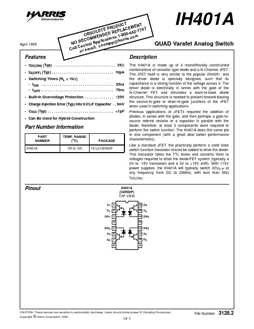
SemiconductorApril 1999IH401AQUAD Varafet Analog SwitchFeatures•r DS(ON) (Typ) . . . . . . . . . . . . . . . . . . . . . . . . . . . . . . 35Ω•I D(OFF) (Typ). . . . . . . . . . . . . . . . . . . . . . . . . . . . . . 10pA •Switching Times (R L = 1k Ω)-t ON . . . . . . . . . . . . . . . . . . . . . . . . . . . . . . . . . . . 25ns -t OFF . . . . . . . . . . . . . . . . . . . . . . . . . . . . . . . . . . . 75ns •Built-In Overvoltage Protection . . . . . . . . . . . . . .±25V •Charge Injection Error (Typ) into 0.01µF Capacitor . . 3mV •C ISS (Typ) . . . . . . . . . . . . . . . . . . . . . . . . . . . . . . . . <1pF •Can Be Used for Hybrid ConstructionDescriptionThe IH401A is made up of 4 monolithically constructed combinations of varacitor type diode and a N-Channel JFET .The JFET itself is very similar to the popular 2N4391, and the driver diode is specially designed, such that its capacitance is a strong function of the voltage across it. The driver diode is electrically in series with the gate of the N-Channel FET and simulates a back-to-back diode structure. This structure is needed to prevent forward biasing the source-to-gate or drain-to-gate junctions of the JFET when used in switching applications.Previous applications of JFETs required the addition of diodes, in series with the gate, and then perhaps a gate-to-source referral resistor or a capacitor in parallel with the diode; therefore, at least 3 components were required to perform the switch function. The IH401A does this same job in one component (with a great deal better performance characteristics).Like a standard JFET, the practically perform a solid state switch function translator should be added to drive the diode.This translator takes the TTL levels and converts them to voltages required to drive the diode/FET system (typically a 0V to -15V translation and a 3V to +15V shift). With ±15V power supplies, the IH401A will typically switch 22V P-P at any frequency from DC to 20MHz, with less than 50Ωr DS(ON).PinoutIH401A (CERDIP)TOP VIEWPart Number InformationPART NUMBER TEMP. RANGE(o C)PACKAGE IH401A-55 to 12516 Ld CERDIP1415169131********45768S 1D 1DR 1DR 2S 2D 2D 4DR 4DR 3S 3D 3S 4CAUTION: These devices are sensitive to electrostatic discharge. Users should follow proper IC Handling Procedures.File Number3128.2O B S OL E T E PR O D U C TN O R E C O M M E N D E D R E P L A C E M E N T C a l l C e n t r a l A p p l i c a t i o n s 1-800-442-7747o r e m a i l: c e n t a p p @ha r r i s .c o mAbsolute Maximum Ratings Thermal InformationSupply VoltageV S to V D . . . . . . . . . . . . . . . . . . . . . . . . . . . . . . . . . . . . . . . . .35V V G to V S, V D. . . . . . . . . . . . . . . . . . . . . . . . . . . . . . . . . . . . . .35V Operating ConditionsTemperature Range . . . . . . . . . . . . . . . . . . . . . . . . . .55o C to 125o C Maximum Junction T emperature (Ceramic Package). . . . . . . . .175o C Storage Temperature Range. . . . . . . . . . . . . . . . . . .-65o C to 150o C Lead T emperature (Soldering, 10s). . . . . . . . . . . . . . . . . . . . .300o CCAUTION: Stresses above those listed in “Absolute Maximum Ratings” may cause permanent damage to the device. This is a stress only rating and operation of the device at these or any other conditions above those indicated in the operational sections of this specification is not implied.Electrical Specifications At 25o C/125o CPARAMETER SYMBOL TEST CONDITIONS MIN TYP MAX UNITS Switch “ON” Resistance r DS(ON)V DRIVE = 15V,V DRAIN = -10V,I D = 10mA-3550ΩPinch-Off Voltage V P I D = 1nA, V DS = 10V245VSwitch “OFF” Current or “OFF” Leakage I D(OFF)V DRIVE = -15V,V SOURCE = -10V,V DRAIN = +10V-10±500pASwitch “OFF” Leakage at 125o C I D(OFF)V DRIVE = -15V,V SOURCE = -10V,V DRAIN = +10V-0.2550nASwitch “OFF” Current I S(OFF)V DRIVE = -15V,V DRAIN = -10V,V SOURCE = +10V-10±500pASwitch “OFF” Leakage at 125o C I S(OFF)V DRIVE = -15V,V SOURCE = -10V,V DRAIN = +10V-0.350nASwitch Leakage When Turned “ON”I D(ON) =I S(ON)V D = V S = -10V,V DRIVE= +15V-0.02±2nAAC Input Voltage Range without Distortion V ANALOG See Figure 22022-V P-P Charge Injection Amplitude V INJECT See Figure 3-3-mV P-PDiode Reverse Breakdown Voltage. This Correlates to Overvoltage Protection BV DIODE V D = V S = -V,I DRIVE = 1µA,DRIVE = 0V-30-45-VGate to Source or Gate to Drain Reverse Breakdown Voltage BV GSS V DRIVE = -V,V D = V S = 0V,DRIVE = 1µA3041-VMaximum Current Switch can Deliver (Pulsed)I DSS V DRIVE = 15V,V S = 0V,D = +10V3555-mA Switch “ON” Time (Note 1)t ON See Figure 1-50-nsSwitch “OFF” Time (Note 1)t OFF See Figure 1-150-nsNOTE:1.Driving waveform must be >100ns rise and fall time.ApplicationsIH401A FamilyIn general, the IH401A family can be used in any application formally using a JFET/isolation diode combination (2N4391or similar). Like standard FET circuits, the IH401A requires a translator for normal analog switch function. The translator is used to boost the TTL input signals to the ±15V analog supply levels which allow the IH401A to handle ±10V analog signals. A typical simple PNP translator is shown in Figure 4.Although this simple PNP circuit represents a minimum of components, it requires open collector TTL input and t (OFF)is limited by the collector load resistor (approximately 1.5µs for 10k Ω). Improved switching speed can be obtained by increasing the complexity of the translator stage.A translator which overcomes the problems of the simple PNP stage is the Harris IH6201 (See Note). This translator driving an IH401A varafet produces the following typical features:NOTE:The IH6201 is a dual translator (two independent translatorsper package) constructed from monolithic CMOS technology.The schematic of one-half IH6201, driving one-fourth of an IH401A, is shown in Figure 5.A very useful feature of this system is that one-half of an IH6201 and one-half of an IH401A can combine to make a SPDT switch, or an IH6201 plus an IH401A can make a dual SPDT analog switch. (See Figure 8)Test CircuitsFIGURE 1.SWITCHING TIME TEST CIRCUIT AND WAVEFORMSFIGURE 2.ANALOG INPUT VOLTAGE RANGE TEST CIRCUIT FIGURE 3.CHARGE INJECTION TEST CIRCUIT-15V+15VSTROBE INPUTSIGNAL V OUT-15V1k Ω+5V+15V 0V -15V10%+5Vt ON90%90%-5V0V 0V 10%10%t OFFt ON 90%t OFF-5V SIGNAL +5V SIGNAL STROBE INPUT1k ΩV IN V OUT+15Vf = 1kHC = 0.01µFV OUT0V-15VFIGURE 4.TYPICAL SIMPLE PNP TRANSLATOR0V+15VR L1/4 OF IH401AFROM TTL OPEN COLLECTOR LOGICANALOG SIGNALS INANALOG OUT 10k Ω+15V-15V 10k Ω•t ON time of approx. 200ns •t OFF time of approx. 80ns break before make switch•TTL compatible strobing levels of•I D(ON)+ I S(ON) typically 20pA up to ±10V analog signals •I D(OFF)or I S(OFF) typically 20pA•Quiescent current drain of approx. 100nA in either “ON” or “OFF” case0.4V2.4VTypical Application Schematic(1/2 of IH401A, Driving 1/4 of an IH401A)Switching InformationNOTE:Either switch is turned on when strobe input goes high.FIGURE 6.DUAL SPST ANALOG SWITCHFIGURE 7.DPDT ANALOG SWITCHNOTE:Each transistor output has a θ and output.θ is just the inverse of θ, i.e., (θ output is 180 degrees out of phase with respect to θ output).FIGURE 5.IH6201 DRIVING AN IH401A0.4V2.4Vθ +15V-15VDV++15V10k ΩGND4k ΩTTL OR CMOS INPUT STROBEV--15V20k Ω2k Ω+5VV L V 1TRANSLATOR (IH6201)1k Ω1k Ωθθ+15V-15VSVARAFETθ -15V+15V14151691312111012345768IH401A14151691312111012345768θ1-15V +5V +15V IH62010V3VT 2L 1θ20V3VT 2L 214151691312111012345768IH401A14151691312111012345768θ1θ1-15V+5V +15V IH62010V3VT 2L 1FIGURE 8.DUAL SPDT ANALOG SWITCHFIGURE 9.DUAL DPST ANALOG SWITCHSwitching Information (Continued)14151691312111012345768IH401A14151691312111012345768θ1θ1θ2θ2T 2L INPUT 1-15V +5V +15V IH6201T 2L INPUT 214151691312111012345768IH401A14151691312111012345768θ1θ2T 2L INPUT-15V +5V +15V IH6201T 2L INPUT。
BTA40,BTA41,BTB4-可控硅 中文自翻资料
Symbol 符号
IT(RMS)
Parameter 参数
On-state rms current 通态均方根电流 TOP3
(full sine wave)
(全正弦波)
RD91 / TOP ins.
通态不重复浪涌电流
ITSM
Non repetitive surge peak on-state current (full cycle, Tj initial = 25 °C)
表1 Table 1.
设备概要 Device summary
Symbol 符号
Parameter 参数
BTA40(1) 注1
BTA41(1) 注1
BTB41
单位 Unit
通态电流有效值 IT(RMS)
断态工作峰值电压Vdrm 反向工作峰值电压Vrrm
VDRM/VRRM
门极触发电流 IGT
On-state rms current 通态均方根电流
VRRM―反向重复峰值电压; 在控制极断路和额定结温的条件下, 可以重复加在可控硅上的交流电压。此电压小于反向最高测试电压100V。反向最高测试电压, 规定为反向漏电流急速增加, 反向特性曲线开始弯曲时的电压。
IGT―门极触发电流; 在额定结温、在阳极和阴极加上一定正向电压(一般为6V)时, 保证元件从阻断状态到导通状态, 加在门极上的最大触发电流。
最后翻译编辑于15-10-06 a1a2x3编
众人拾柴火焰高
希望后来完善的朋友, 可以更新一下左边的时间日期
和编者名, 以方便后来者整理
by:a1a2x3
BTA40, BTA41, BTB41
40 A standard TRIACs
特征 Features
世图兹精密空调产品介绍之欧阳育创编

世图兹精密空调产品介绍CCD201A性能参数:机组尺寸宽深高(mm)10008101850机组尺寸宽深高(mm)1880770910(单组)德国世图兹Minispace系列机房专用空调介绍Minispace系列描述:高适应性:多项节能设计多种送风方式,满足不同气流组织需求多种冷却方式,包括风冷、水冷、冷冻水等,有利于适应现场的实际条件;监控管理方式多样,适合各种系统;占地面积小,制冷效果佳;采用符合EU4标准的高效空气过滤系统;风冷方式提供超远安装距离和超高落差的方案;前开门设计,便于安装和维护;Minispace机组特点:德国STULZ Minispace产品,该产品系列在同行业产品中,技术成熟可靠,性价比高,产品系列晚辈,具有多种制冷方式机组,多种送风方式选择,具有高实用性、高稳定性的特点。
Minispace空调产品系列是在采用新的设计理念和创新技术而形成的经典一代高可靠性和高科技产品系列。
该系列产品具有独特的性能特点:节能、高可靠性、环保、低噪、风量大、方便。
1、STULZ Minispace系列空调具有高显热比特点:通讯机房内电子设备释放出大量的显热。
Minispace针对机房特点实现0.9以上的高显热比,在机房环境下使用,相对于普通舒适性空调节省20-30%的能耗,并因此避免过度除湿和送风带雾。
2、功能强大的新一代C5000微处理控制器控制器是空调系统的核心。
在以前C1002控制器的基础上性能有了进一步的提高,技术不断更新的STULZ新一代的控制器C5000采用先进的“模糊”控制理论作为其控制的基础,可对机房环境-温度、湿度、洁净度进行连续的24小时精密控制,并具有自学习、分析、预测、自动控制功能,是一种新型智能控制器。
1)大屏幕汉语显示,方便用户使用;2)可显示24小时温、湿度曲线,简学、清晰、明显;3)可实现对空调机组的分散独立的智能化控制;4)记录各功能部件的运行时间,如制冷、加热、加湿、除湿等;5)80条报警记录,且有断电数据保护;6)在机组出现高压或者低压警告和停机,可实现自动重启功能,停电机组也具有来电自启动功能,避免不必要的到场工作,满足无人值守的要求;7)控制板可配置标准RS485通信接口,,与BMS 连接时无需额外的硬件支出,可接打印机;8)机房参数的三级控制:参数新型的显示监控,报警参数的设置,系统基本功能的设置。
10G GPON产品介绍(R11&R311)

Anna Cui (AT&T), Fabrice Bourgart (FT), Junichi Kani (NTT)
G.987.2
Rapporteur: Frank Effenberger (Huawei)
PMD & RE
Richard Goodson (Adtran), Joe Smith (ALU)
HUAWEI TECHNOLOGIES CO., LTD.
Huawei Confidential
Page 11
G.987.3 V.S. G.984.3 - 增强和改进
功能 子项 下行GTC 成帧 上行GTC GEM
G.984.3 基本帧结构一致 具体的帧域内容不同
G.987.3
参见胶片Page 11 - 13
对已部署的GPON ODN网络无影响
XGPON U/S
GPON U/S
GPON D/S
XGPON D/S
波长范围
1260 1280 1290 1330 1480 1500 1575 1580
XG-ONU ONU XG-ONU XG-ONU ONU ONU
WDM overlay
XG-OLT
WDM1r
类型 尺寸 温度范围 网络侧接口 用户侧 固定配置
半插卡式设备 1U,19英寸 WxDxH: 442mm×220mm×43.6mm -25 ℃ ~ + 65 ℃ 支持10G GPON,EPON,GPON, GE,10G EPON 2GE+6FE+16POTS; 2GE+6FE;
插卡类型 语音协议 时钟、时间 供电、备电方式 散热方式 防护机制
2.48832 Gb/s D/S 1480-1550nm DS 1290-1330nm US 32/64 20 km (Logical: 60 km) 20Km ClassB: 10- 25dB Class B+: 13-28dB ClassC: 15-30dB ClassC+: 17-32dB
MCP41010数据手册中文版

概述
MCP41XXX 和 MCP42XXX 器件是具有 256 个抽头的数 字电位器,有 10 kΩ、 50 kΩ 和 100 kΩ 3 种电阻选择。 MCP41XXX 是单通道器件, 有 8 引脚 PDIP 和 SOIC 两 种封装形式。 MCP42XXX 是双通道器件,有 14 引脚 PDIP、 SOIC 或 TSSOP 三种封装形式。 MCP41XXX/ 42XXX 的抽头位置在工业级 SPI 接口控制下线性变化。 此器件的静态工作电流 < 1 µA。 软件关断功能可将 “A” 端与电阻阵列断开,同时将抽头连接到“B”端。此外, 双通道 MCP42XXX 还有一个 SHDN 引脚,可通过硬件 实现上述相同功能。在关断模式期间,能更改抽头控制 寄存器的内容,电位器在退出关断模式后将使用新值。 在上电时抽头复位到半量程 (80h) 。通过 RS (复位) 引脚执行硬件复位并将抽头返回半量程。 MCP42XXX SPI 接口包括 SI 和 SO 引脚,允许使用菊花链连接多个 器件。 MCP42XXX 上通道与通道的电阻匹配变化小于 1%。这些器件使用 2.7 - 5.5V 单电源供电,并可在扩展 级和工业级温度范围下工作。
ppm/°C 编码 80h
, RS 和 SHDN 引脚的工作方式请参见图 2-12 数字输入 / 输出 (CS、 SCK、 SI 和 SO)
VAB = VDD,抽头上无连接。 变阻器位置非线性度 R-INL 是指抽头在最大电阻和最小电阻范围内测量的实际位置偏离理想位置的程度。 R-DNL 测量连续抽头位置 间的步长相对理想值的变化。对于 10 kΩ 的电位器, VDD = 3V 时 IW = 50 µA, VDD = 5V 时 IW = 400 µA。测试电路请参见图 2-26。 在器件配置为分压器或电位器模式时,在 VW 上测量 INL 和 DNL。 VA = VDD 且 VB = 0V。 DNL 规范极限值 ±1 LSB (最大值)是在规 定的单调操作条件下的值。测试电路请参见图 2-25。 电阻端子 A、 B 和 W 相互间无极性限制。满量程误差和零刻度误差使用图 2-25 进行测量。 在 VW 引脚上测得,此时该引脚附近的另一个 VW 引脚上的电压满幅摆动。 供电电流与流经电位器的电流无关。
SF14中文资料

Features·Low Leakage·Low Forward Voltage Drop ·High Current Capability·Super-fast Switching Speed < 35ns ·Plastic Material: UL Flammability Classification Rating 94V-0Mechanical Data·Case: Molded Plastic·Terminals: Plated Axial Leads, Solderable per MIL-STD-202 Method 208·Polarity: Color Band Denotes Cathode ·Approx. Weight: 0.3 grams ·Mounting Position: AnyRatings at 25°C ambient temperature unless otherwise specified.Single phase, half wave, 60Hz, resistive or inductive load.Maximum Ratings and Electrical CharacteristicsCharacteristicSymbol SF11SF12SF13SF14Unit Maximum Recurrent Peak Reverse Voltage V RRM 50100150200V Maximum RMS Voltage V RMS 3570105140V Maximum DC Blocking voltageV DC 50100150200V Maximum Average Forward Rectified Current .375"9.5mm Lead Length @ T A =55°C I (AV) 1.0A Peak Forward Surge Current 8.3 ms single half sine-wave superimposed on rated load (JEDEC method)I FM 30A Maximum Instantaneous Forward Voltage at 1.0A DCV f 0.975V Maximum DC Reverse Current at Rated DC Blocking VoltageI R 5.0m A Maximum DC Reverse Current at Rated DC Blocking Voltage @ T A = 150°C I R 50m A Maximum Reverse Recovery Time (Note 1)T rr 35ns Typical Junction Capacitance (Note 2)C J 63pF Operating and Storage Temperature RangeT J ,T STG-65 to + 175°CNotes:1. Reverse Recovery Test Conditions: I F =0.5 A, I R =1.0 A,I RR =0.25A2. Measured at 1.0MHz and applied reverse voltage of 4.0V.SF11 - SF141.0A SUPER-FAST RECOVERY RECTIFIERAAB CDDO-41Dim Min Max A 25.4—B 4.1 5.2C 0.710.86D2.02.7All Dimensions in mm0.010.11.010I N S T A N T A N E O U S R E V E R S E C U R R E N T (m A )PERCENT OF PEAK REVERSE VOLTAGE Fig.2Typical Reverse Characteristics0.0010.010.11.01000.20.40.60.8 1.0 1.2 1.4I N S T A N T A N E O U S F O R W A R D C U R R E N T (A )INSTANTANEOUS FORWARD VOLTAGE (V)Fig.3Typ.Instantaneous Fwd Characteristics10203040P E A K F O R W A R D S U R G E C U R R E N T (A M P E R E S )NUMBER OF CYCLESAT 60HzFig.4Max Non-Repetitive Peak Fwd Surge Current (A)10203040700.1 1.010*******J U N C T I O N C A P A C I T A N C E (p F )REVERSE VOLTAGE (VOLTS)Fig.5Typical JunctionCapacitance1.00255075100125150175A V E R A G E F O R W A R D C U R R E N T (A M P E R E S )AMBIENT TEMPERATURE (ºC)Fig.1Typical Forward Current Derating Curve。
Genuinetek蜂易达手机信号放大器选型指南

Genuinetek蜂易达手机信号放大器选型指南家庭用户信号不好存在多种情况,根据不同情况,应选用不同的手机信号放大器。
针对不同情况有不同的解决方案,不可一刀切。
底层小区信号差室外街道有较好的信号,室内信号较差,这个是一般的情况,主要是周边的建筑把基站的信号挡住了造成的。
这种情况是很常见的,可以加装Genuinetek蜂易达FX-Std系列信号放大器解决。
农村、郊区信号差室外有微弱信号,室内基本没有信号,信号差是由于农村、郊区基站不够密集,有些地方距离基站较远,造成了信号微弱。
应选用TX侧输出功率较高,增益较大的FX-HS系列提高最大传输距离。
大型厂房、别墅信号差室外街道有较好信号,室内基本没有信号,信号差是由于别墅、厂房的房间里面的钢筋混凝土很难被900Mhz左右频率的手机信号穿过,信号被挡住了,应选用蜂易达RX侧最大输出功率较高的FX-Pro提高室内覆盖面积。
高层信号差高层的手机信号差的原因和以上几点都不同,其实高层的手机信号并不差,那为什么会仍然打不通电话呢?主要是因为高层可以接收到附近好几个基站传过来的信号,然而因为没有阻挡,所以信号强度也差不多,于是手机就会在几个基站之间频繁地切换,这就是所谓的“乒乓效应”;另外,手机还有可能会收到非相邻的基站的信号,由于手机只能在相邻的基站间进行切换,就会造成其实有一个更好信号的基站的信号手机能收到,却由于基站不相邻无法切换过去,造成所谓的“孤岛效应”。
据介绍,乒乓效应和孤岛效应是目前移动通信的难题,加装第二代的蜂信通手机信号放大器高层版可以有效改善,其原理和解决方案也跟上述情况不同。
乒乓效应会造成手机频繁切换经常掉线,孤岛效应会造成手机脱网。
Genuinetek 蜂易达的FX-Pro可以有效解决乒乓效应和孤岛效应。
越区切换因为越区切换不成功也会造成手机掉线。
移动的运营商是通过基站和手机发送电磁波通信而为用户服务的。
然后一般基站都是蜂窝状的,覆盖范围有限,在一个较大的区域内有可能会同时有几个不同的基站。
Vishay Semiconductors TFDU4101 无线短距离通信模块技术参数说明说明书

Infrared Transceiver Module (SIR, 115.2 kbit/s) for IrDA®ApplicationsDESCRIPTIONThe TFDU4101 transceiver is an infrared transceiver module compliant to the latest IrDA® physical layer standard for fast infrared data communication, supporting IrDA speeds up to 115.2 kbit/s (SIR), and carrier based remote control modes. Integrated within the transceiver module are a photo pin diode, an infrared emitter (IRED), and a low-power control IC to provide a total front-end solution in a single package. This device covers the full IrDA range of more than 1 m using the internal intensity control. With one external current control resistor the current can be adjusted for shorter ranges saving operating current operating in IrDA low power mode. This Vishay SIR transceiver is using the lead frame technology.The receiver output pulse duration is independent of the optical input pulse duration and recovers always a fixed pulse duration optimum for compatibility to standard Endecs and interfaces. TFDU4101 has a tristate output and is floating in shutdown mode with a weak pull-up.FEATURES•Operates from 2.4 V to 5.5 V within specification over full temperature range from- 30 °C to + 85 °C•Split power supply, transmitter and receivercan be operated from two power supplieswith relaxed requirements saving costs,US - patent no. 6,157,476•Low power consumption (< 0.12 mA supply current in receive mode, no signal)•Power shutdown mode (< 4 μA shutdown current in full temperature range, up to 85 °C, < 10 nA at 25 °C) •Surface mount package (L x W x H in mm): 9.7 × 4.7 × 4•High efficiency emitter•Low profile (universal) package capable of surface mount soldering to side and top view orientation•Directly Interfaces with various super I/O and controller devices as e. g. TOIM4232•Tri-state-receiver output, floating in shut down with a weak pull-up•Qualified for lead (Pb)-free and Sn/Pb processing (MSL4)•Material categorization: For definitions of compliance please see /doc?99912 APPLICATIONS•Printers, fax machines, photocopiers, screen projectors •Internet TV boxes, video conferencing systems•Medical data collection•Diagnostic systems•Notebook computers, desktop PCs, palmtop computers (Win CE, Palm PC), PDAs•Internet TV boxes, video conferencing systems •External infrared adapters (dongles)•Data loggers•GPS•Kiosks, POS, point and pay devices•Industrial applications PRODUCT SUMMARYPART NUMBER DATA RATE(kbit/s)DIMENSIONSH x L x W(mm x mm x mm)LINK DISTANCE(m)OPERATINGVOLTAGE(V)IDLE SUPPLYCURRENT(mA)TFDU4101115.2 4 x 9.7 x 4.70 to ≥ 1 2.4 to 5.50.07PARTS TABLEPART DESCRIPTION QTY/REEL TFDU4101-TR3Oriented in carrier tape for side view surface mounting1000 pcs TFDU4101-TT3Oriented in carrier tape for top view surface mounting1000 pcsFUNCTIONAL BLOCK DIAGRAMPIN DESCRIPTIONPINNUMBERSYMBOL DESCRIPTION I/O ACTIVE1V CC2IRED anodeIRED anode to be externally connected to V CC2. An external resistor isonly necessary for controlling the IRED current when a current reduction below 300 mA is intended to operate in IrDA low power mode.This pin is allowed to be supplied from an uncontrolled power supplyseparated from the controlled V CC1 - supply.2IRED cathode IRED cathode, internally connected to driver transistor3TXD This Schmitt-Trigger input is used to transmit serial data when SD is low.An on-chip protection circuit disables the LED driver if the TXD pin isasserted for longer than 50 μs (max. 300 μs).I High4RXD Received data output, push-pull CMOS driver output capable of drivingstandard CMOS or TTL loads. During transmission the RXD output isactive (echo-on). No external pull-up or pull-down resistor is required.Floating with a weak pull-up of 500 k (typ.) in shutdown mode.O Low5SD Shutdown I High 6V CC1Supply voltage7NC No internal connection I8GND GroundPINOUTTFDU4101 Weight 200 mgNote•Reference point pin, GND unless otherwise noted. Typical values are for DESIGN AID ONLY, not guaranteed nor subject to production testing.Note•Vishay transceivers operating inside the absolute maximum ratings are classified as eye safe according the above table.ABSOLUTE MAXIMUM RATINGSPARAMETER TEST CONDITIONS SYMBOL MIN.TYP.MAX.UNIT Supply voltage range, transceiver- 0.3 V < V CC2 < 6 V V CC1- 0.56V Supply voltage range, transmitter - 0.5 V < V CC1 < 6 V V CC2- 0.56V Voltage at RXD- 0.5 V < V CC1 < 6 V V RXD - 0.5V CC1 + 0.5V Voltage at all inputs and outputs V in > V CC1 is allowedV in- 0.56V Input currents For all pins, except IRED anode pin10mA Output sinking current 25mA Power dissipation See derating curveP D 250mW Junction temperature T J 125°C Ambient temperature range (operating)T amb - 30+ 85°C Storage temperature range T stg- 30+ 85°C Soldering temperature See “Recommended Solder Profile”260°C Average output current, pin 1I IRED (DC)80mA Repetitive pulse output current, pin 1 to pin 2< 90 μs, t on < 20 %I IRED (RP)400mAEYE SAFETY INFORMATIONSTANDARDCLASSIFICATIONIEC/EN 60825-1 (2007-03), DIN EN 60825-1 (2008-05) “SAFETY OF LASER PRODUCTS - Part 1: equipment classification and requirements”, simplified methodClass 1IEC 62471 (2006), CIE S009 (2002) “Photobiological Safety of Lamps and Lamp Systems”Exempt DIRECTIVE 2006/25/EC OF THE EUROPEAN PARLIAMENT AND OF THE COUNCIL of 5th April 2006 on the minimum health and safety requirements regarding the exposure of workers to risks arising from physical agents (artificial optical radiation) (19th individual directive within the meaning of article 16(1) of directive 89/391/EEC)ExemptNotes•T amb = 25 °C, V CC1 = V CC2 = 2.4 V to 5.5 V unless otherwise noted.•Typical values are for DESIGN AID ONLY, not guaranteed nor subject to production testing.(1)Standard illuminant A.(2)The typical threshold level is 0.5 x V CC1. It is recommended to use the specified min./max. values to avoid increased operating current.ELECTRICAL CHARACTERISTICSPARAMETER TEST CONDITIONS/PINSSYMBOL MIN.TYP.MAX.UNIT TRANSCEIVER Supply voltage V CC12.4 5.5V Dynamic supply currentSD = low, E e = 1 klx (1),T amb = - 25 °C to + 85 °C V CC1 = V CC2 = 2.4 V to 5.5 V I CC14090130μADynamic supply current SD = low, E e = 1 klx (1),T amb = 25 °CV CC1 = V CC2 = 2.4 V to 5.5 VI CC14075μA Average dynamic supply current, transmittingI IRED = 300 mA,25 % duty cycleI CC 0.65 2.5mA Shutdown supply currentSD = high, T = 25 °C, E e = 0 klx no signal, no resistive loadI SD 0.010.1μA SD = high, T = 70 °C no signal, no resistive load I SD 1μA SD = high, T = 85 °C no signal, no resistive loadI SD 1μA Operating temperature range T A - 30+ 85°C Output voltage low, RXD C load = 15 pFV OL - 0.50.15 x V CC1V Output voltage high, RXD I OH = - 500 μA, C Load = 15 pF V OH 0.8 x V CC1V CC1 + 0.5V I OH = - 250 μA, C Load = 15 pF V OH 0.9 x V CC1V CC1 + 0.5V RXD to V CC1 impedance R RXD 400500600k ΩInput voltage low (TXD, SD)V IL - 0.50.5V Input voltage high (TXD, SD) 1.5 V ≤ V logic ≤ 2.5 V (2)V IH 0.8 x V CC16V V logic > 2.5 V (2)V IH V CC1 - 0.56V Input leakage current (TXD, SD)V in = 0.9 x V CC1I ICH - 2+ 2μA Controlled pull down current 0 < V in < 0.15 V CC1 V in > 0.7 V CC1SD, TXD = “0” or “1”I IrTX - 10+ 1501μA μA Input capacitance (TXD, SD)C I5pFNotes (3)T amb = 25 °C, V CC1 = V CC2 = 2.4 V to 5.5 V unless otherwise noted.Typical values are for DESIGN AID ONLY, not guaranteed nor subject to production testing. (4)IrDA specification is 40 mW/m 2. Specification takes a window loss of 10 % into account.(5)IrDA sensitivity definition: minimum irradiance E ein angular range, power per unit area. The receiver must meet the BER specification while the source is operating at the minimum intensity in angular range into the minimum half-angular range at the maximum link length.(6)Maximum irradiance E ein angular range, power per unit area. The optical delivered to the detector by a source operating at the maximum intensity in angular range at minimum link length must not cause receiver overdrive distortion and possible ralated link errors. If placed at the active output interface reference plane of the transmitter, the receiver must meet its bit error ratio (BER) specification.(7)Using an external current limiting resistor is allowed and recommended to reduce IRED intensity and operating current when current reduction is intended to operate at the IrDA low power conditions. E.g. for V CC2 = 3.3 V a current limiting resistor of R S = 56 Ω will allow a power minimized operation at IrDA low power conditions.(8)Due to this wavelength restriction compared to the IrDA spec of 850 nm to 900 nm the transmitter is able to operate as source for the standard remote control applications with codes as e.g. Phillips RC5/RC6® or RECS 80.For more definitions see the document “Symbols and Terminology” on the Vishay website.OPTOELECTRONIC CHARACTERISTICS (1)PARAMETER TEST CONDITIONSSYMBOLMIN.TYP.MAX.UNITRECEIVERMinimum irradiance E e in angular range (3) SIR mode 9.6 kbit/s to 115.2 kbit/sλ = 850 nm to 900 nm; α = 0°, 15°E e, min.4(0.4)20(2)35 (2)(3.5)mW/m 2 (μW/cm 2)Maximum irradiance E e in angular range (4)λ = 850 nm to 900 nm E e, max.5(500)kW/m 2 (mW/cm 2)Rise time of output signal 10 % to 90 %, C L = 15 pF t r (RXD)20100ns Fall time of output signal 90 % to 10 %, C L = 15 pF t f (RXD)20100ns RXD pulse width Input pulse length > 1.2 μs t PW1.652.23μs Leading edge jitter Input irradiance = 100 mW/m 2,≤ 115.2 kbit/s 250ns Standby/shutdown delay, receiver startup time After shutdown active or power-on500μs Latency t L100150μsTRANSMITTER IRED operating current, switched current limiter No external resistor for current limitation (5)I D 250300350mA Forward voltage of built-in IREDI f = 300 mAV f 1.4 1.81.9V Output leakage IRED current I IRED - 11μA Output radiant intensity α = 0°, 15°TXD = high, SD = lowI e 4865mW/sr Output radiant intensity V CC1 = 5 V, α = 0°, 15°TXD = low or SD = high (receiver is inactiveas long as SD = high)I e 0.04mW/sr Output radiant intensity, angle of half intensityα± 24deg Peak - emission wavelength (6)λp 880900nm Spectral bandwidth ∆λ45nm Optical rise time, optical fall timet ropt , t fopt10300ns Optical output pulse duration Input pulse width 1.6 μs < t TXD < 20 μs t opt t TXD - 0.15t TXD + 0.15μs Optical output pulse duration Input pulse width t TXD ≥ 20 μst opt20300μs Optical overshoot25%RECOMMENDED CIRCUIT DIAGRAMOperated with a clean low impedance power supply the TFDU4101 needs no additional external components. However, depending on the entire system design and board layout, additional components may be required (see figure 1). That is especially the case when separate power supplies are used for bench tests. When using compact wiring and regulated supplies as e. g. in phone applications in most cases no external components are necessary.Fig. 1 - Recommended Test CircuitNote*) R1 is optional when reduced intensity is used.The capacitor C 1 is buffering the supply voltage and eliminates the inductance of the power supply line. This one should be a Tantalum or other fast capacitor to guarantee the fast rise time of the IRED current. The resistor R1 is the current limiting resistor, which may be used to reduce the operating current to levels below the specified controlled values for saving battery power.Vishay's transceivers integrate a sensitive receiver and a built-in power driver. The combination of both needs a careful circuit board layout. The use of thin, long, resistive and inductive wiring should be avoided. The shutdown input must be grounded for normal operation, also when theshutdown function is not used.The inputs (TXD, SD) and the output RXD should be directly connected (DC-coupled) to the I/O circuit. The capacitor C2 combined with the resistor R2 is the low pass filter for smoothing the supply voltage. R2, C1 and C2 are optional and dependent on the quality of the supply voltages V CC1and injected noise. An unstable power supply with dropping voltage during transmission may reduce the sensitivity (and transmission range) of the transceiver.The placement of these parts is critical. It is strongly recommended to position C 2 as close as possible to the transceiver power supply pins.When extended wiring is used (bench tests!) the inductance of the power supply can cause dynamically a voltage drop at V CC2. Often some power supplies are not able to follow the fast current rise time. In that case another 4.7 μF (type, see table under C1) at V CC2 will be helpful.Under extreme EMI conditions as placing an RF-transmitter antenna on top of the transceiver, we recommend to protect all inputs by a low-pass filter, as a minimum a 12 pF capacitor, especially at the RXD port. The transceiver itself withstands EMI at GSM frequencies above 500 V/m. When interference is observed, the wiring to the inputs picks it up. It is verified by DPI measurements that as long as the interfering RF - voltage is below the logic threshold levels of the inputs and equivalent levels at the outputs no interferences are expected.One should keep in mind that basic RF-design rules for circuit design should be taken into account. Especially longer signal lines should not be used without termination. See e.g. "The Art of Electronics" Paul Horowitz, Winfield Hill, 1989, Cambridge University Press, ISBN: 0521370957.Figure 2 shows an example of a typical application with a separate supply voltage V S and using the transceiver with the IRED anode connected to the unregulated battery V batt . This method reduces the peak load of the regulated power supply and saves therefore costs. Alternatively all supplies can also be tied to only one voltage source. R1 and C1 are not used in this case and are depending on the circuit design in most cases not necessary.In figure 2 an option is shown to operate the transmitter at two different power levels to switch for long range to lowpower mode for e.g. saving power for IrDA application but use the full range specification for remote control. The additional components are marked in the figure.For operating at RS232 ports TOIM4232 is recommendedas ENDEC.TABLE 1 - RECOMMENDED TESTS AND APPLICATION CIRCUIT COMPONENTSCOMPONENTRECOMMENDED VALUEVISHAY PART NUMBERC1 4.7 μF, 16 V 293D 475X9 016B C20.1 μF, ceramic VJ 1206 Y 104 J XXMT R1Depends on current to be adjusted, e. g. with V CC2 = 3.3 V 56 Ω is an option for minimum low power operationR247 Ω, 0.125 WCRCW-1206-47R0-F-RT1Fig. 2 - Typical Application CircuitGrey: Optional for High/Low SwitchingI/O AND SOFTWAREIn the description, already different I/Os are mentioned. Different combinations are tested and the function verified with the special drivers available from the I/O suppliers. In special cases refer to the I/O manual, the Vishay application notes, or contact directly Vishay Sales, Marketing or Application.CURRENT DERATING DIAGRAMFigure 3 shows the maximum operating temperature when the device is operated without external current limiting resistor.Fig. 3 - Current Derating DiagramTABLE 2 - TRUTH TABLEINPUTS OUTPUTS REMARKSD TXD OPTICAL INPUT IRRADIANCEmW/m2RXD TRANSMITTER OPERATIONHigh > 1 ms x xWeakly pulled(500 k ) to V CC10ShutdownLow High < 50 μs x Low active I e TransmittingHigh > 50 μs x High inactive0Protection is active Low< 4High inactive0Ignoring low signals below theIrDA defined threshold for noiseimmunity Low> min. irradiance E e< max. irradiance E eLow (active)0Response to an IrDA compliantoptical input signal Low> max. irradiance E e Undefined0Overload conditions can causeunexpected outputsRECOMMENDED SOLDER PROFILES Solder Profile for Sn/Pb SolderingFig. 4 - Recommended Solder Profile for Sn/Pb SolderingLead (Pb)-free, Recommended Solder ProfileThe TFDU4101 is a lead (Pb)-free transceiver and qualified for lead (Pb)-free processing. For lead (Pb)-free solder paste like Sn(3.0-4.0)Ag(0.5-0.9)C u, there are two standard reflow profiles: Ramp-Soak-Spike (RSS) and Ramp-To-Spike (RTS). The Ramp-Soak-Spike profile was developed primarily for reflow ovens heated by infrared radiation. With widespread use of forced convection reflow ovens the Ramp-To-Spike profile is used increasingly. Shown below in figure 5 and 6 are Vishay's recommended profiles for use with the TFDU4101 transceivers. For more details please refer to the application note “SMD Assembly Instructions”.A ramp-up rate less than 0.9 °C/s is not recommended. Ramp-up rates faster than 1.3 °C/s could damage an optical part because the thermal conductivity is less than compared to a standard IC.Wave SolderingFor TFDUxxxx and TFBSxxxx transceiver devices wave soldering is not recommended.Manual SolderingManual soldering is the standard method for lab use. However, for a production process it cannot be recommended because the risk of damage is highly dependent on the experience of the operator. Nevertheless, we added a chapter to the above mentioned application note, describing manual soldering and desoldering.StorageThe storage and drying processes for all Vishay transceivers (TFDUxxxx and TFBSxxx) are equivalent to MSL4.The data for the drying procedure is given on labels on the packing and also in the application note “Taping, Labeling, Storage and Packing”. Fig. 5 - Solder Profile, RSS Recommendation Fig. 6 - RTS RecommendationPACKAGE DIMENSIONS in millimetersFig. 7 - Package Drawing TFDU4101. Tolerance ± 0.2 mm if not otherwise mentionedFig. 8 - Recommended Footprint for Side View Applications and Solderpaste MaskFig. 9 - Recommended Footprint for Top View Applications and Solderpaste MaskREEL DIMENSIONSin millimetersTAPE WIDTH(mm)A MAX.(mm)N (mm)W 1 MIN.(mm)W 2 MAX.(mm)W 3 MIN.(mm)W 3 MAX.(mm)243306024.430.423.927.4TAPE DIMENSIONS in millimetersFig. 10 - Tape Drawing, TFDU4101 for Top View Mounting, Tolerance ± 0.1 mmHANDLING PRECAUTIONSagging of carrier tape may cause some units to rotate and will result to pick-and-place problem. Do not allow carrier tape to sag as shown in picture below.Fig. 11 - Tape Drawing, TFDU4101 for Side View Mounting, Tolerance ± 0.1 mmLegal Disclaimer Notice VishayDisclaimerALL PRODUCT, PRODUCT SPECIFICAT IONS AND DAT A ARE SUBJECT T O CHANGE WIT HOUT NOT ICE T O IMPROVE RELIABILITY, FUNCTION OR DESIGN OR OTHERWISE.Vishay Intertechnology, Inc., its affiliates, agents, and employees, and all persons acting on its or their behalf (collectively, “Vishay”), disclaim any and all liability for any errors, inaccuracies or incompleteness contained in any datasheet or in any other disclosure relating to any product.Vishay makes no warranty, representation or guarantee regarding the suitability of the products for any particular purpose or the continuing production of any product. To the maximum extent permitted by applicable law, Vishay disclaims (i) any and all liability arising out of the application or use of any product, (ii) any and all liability, including without limitation special, consequential or incidental damages, and (iii) any and all implied warranties, including warranties of fitness for particular purpose, non-infringement and merchantability.Statements regarding the suitability of products for certain types of applications are based on Vishay’s knowledge of typical requirements that are often placed on Vishay products in generic applications. Such statements are not binding statements about the suitability of products for a particular application. It is the customer’s responsibility to validate that a particular product with the properties described in the product specification is suitable for use in a particular application. Parameters provided in datasheets and / or specifications may vary in different applications and performance may vary over time. All operating parameters, including typical parameters, must be validated for each customer application by the customer’s technical experts. Product specifications do not expand or otherwise modify Vishay’s terms and conditions of purchase, including but not limited to the warranty expressed therein.Except as expressly indicated in writing, Vishay products are not designed for use in medical, life-saving, or life-sustaining applications or for any other application in which the failure of the Vishay product could result in personal injury or death. Customers using or selling Vishay products not expressly indicated for use in such applications do so at their own risk. Please contact authorized Vishay personnel to obtain written terms and conditions regarding products designed for such applications.No license, express or implied, by estoppel or otherwise, to any intellectual property rights is granted by this document or by any conduct of Vishay. Product names and markings noted herein may be trademarks of their respective owners.。
TESA RUGOSURF 10G 和 RUGOSOFT 10G 表面粗糙度测试仪商品说明书

TESA RUGOSURF 10GSurface roughness gageTESA –TECHNOLOGYGenuine Swiss MadeQualityRUGOSURF 10G is a portable and versa-tile roughness gage that can be used in theworkshop, for incoming inspection or in thelaboratory. This heavy-duty hand-held tooloffers a wide range of accessories and canbe used in a number of applications that’svirtually unlimited.Technical DataTable of measured roughness parametersInternational StandardsISO 4287Ra Rq Rt Rz Rp Rv Rc RSm Rδc Rpc1997Rk Rpk Rvk Mr1Mr2Pa Pq Pt Pp Pv Pc Psm Pδc Ppc Din Rmax R3z R3zmISO 12085R AR Rx Rke Rpke RykeMeasuring range0 + 300 µm / 0 +12µinResolution0.005µm / 0.02µinCut-offs (I c in in)0.01 in0.03 in0.1 inTotal length(I m in in)0.05 in0.15 in0.5 inTraversing length(I c in in)0.06 in0.18 in0.6 inPossible selection of 2,3,4 or 5 cut-offsfor the measurement (length from 0.75 to 16 mm)J-2TESA RUGOSOFT 10GOrder No.EDP No.0693001124720TESA RUGOSOFT SoftwareComplete with:- CD ROM for installation in 5 languages- RS 232 Connection Cable- On-line instruction Manual (included on installation CD)Order No.EDP No.0696003423126Optional ProbesSB10 - For regular surface finish and bores.External diameters > .4"/10mm and internal diameters from 25"/6mmOrder No.EDP No.0696003623128SB20 - For slots with depths up to .2"/5mm max.Order No.EDP No.0696003723129SB30 - For small bores with a 15"/4mm minimum diameter,.8"/20mm in depth.Order No.EDP No.0696003823130SB40 - With a prismatic contact skid formeasuring cables. External diameters > 04"/1mm.Order No.EDP No.06960039231331SB50 - With front mounted contact skid for inspectingconcave surfaces.Ideal for measuring through to 90°.Order No.EDP No.Price0696004023132$719.00Standard AccessoriesSupport with Granite Base, 15.75" x 9.85" (400mm x 200mm)Order No.EDP No.0696003523127Roughness Specimen, Ra = 117 µin/2.97 µmOrder No.EDP No.0696004123133External Control SwitchOrder No.EDP No.0696004223134Additional accessories available upon requestJ-3J -4Summary of Roughness Parameters Commonly UsedArithmetical mean deviation of the profile R a (ISO 4287, DIN 4768)The arithmetical mean deviation R a is the mean value of the absolute value of the profile departure y within the reference length l.Max. profile valley depth R max (DIN 4768)Among the existing single roughness depths Z i , the max. profile valley depth R max counts for the most significant within the total measuring length l m .According to ISO 4288 and DIN 4287 - Part 1, this parameter is also specified as R y max .Mean roughness depth R z DIN (DIN 4768)The mean roughness depth R z is the arithmetical mean of the single rough-ness depths of successive sampling lengths l e .According to ISO 4287 and DIN 4762, the parameter R z DIN is also specified as R y5.Because R z is named differently in DIN 4768 and ISO 4287, this para m ater is also specified as R z DIN or R z ISO .When the parameter R z is measured according to DIN, it is generally admit-ted that the extreme value ISO is also matched providing that R z ISO is not exceeding R z DIN .Application of Roughness Comparison SpecimensThese specimens for testing the surface finish quality have long proven their value in practical use.They serve for touch and/or sight comparisons with the surface of the work-pieces that are manufactured using the same method. Condition is that materials have to be comparable.The comparison of the roughness of the workpiece surface is not quantitativelyexpressed. The extent to which the surfaces of both the specimen and the workpiece are matched is appreciated subjectively only.Sight comparison requires optimum light source angle. For small surfaces, the use of a magnifying glass with up to 8x magnifica-tion is recommended.Touch comparison is made using the finger nail or a small copper piece like a coin, for instance.5 x l Z Z Z Z Z 12345m a xR l = l t ee mI 0lyR amxPre-coursePost-courseJ -50693000029527Rugosurf 100 S, for probes with contact skids 0693000129910Rugosurf 100 SF, for probes without contact skids0693000229911Rugosurf 100 S-CNOMO, for probes with contact skids 0693000329912Rugosurf 100 SF-CNOMO, for probes without contact skidsProbe system:Hall Effect Technology,analogue with high-linear output signal.90° diamond stylus, radius 5 μm25 mm contact skid (TESA standard probe STS)Stylus force in staticmeasuring: < 0,5 mN (DIN 4772)Resting force on contact skids: < 0,15 mN Class 1 (± 5%) as per DIN 4772Linearity: < 2% throughout the measuring range,t emperature compensation from 0 to 60 °C Probing speed:0,8 mm/sReverse speed: approx. 2,0 mm/sRechargeableb atteries with μP controlled check Thermal printer for all measured values plus curve t pRS-232 digital output 80%, with no con-densation 10 °C to 40 °C 130 x 78 x 245 mm 700 gSuited plastic case Declaration of conformityTESA Surface Roughness Gage RUGOSURF 100Versatile roughness gauge designed for measuring roughness parameters according to ISO 4287/1, DIN 4768, 4772, 4777 or CNOMO (ISO 12085). A wide variety of interchangeable probes allows you to solve specificapplications, such as roughness measurements on surfaces of grooves, small bores, cylinders, steel balls etc.•Measured parameters: R a , R z DIN , R max , R 3z , R t , R q RMS along with printed profile bearing portion t p .•Integrated thermal printer.•Choice of cut-offs from 0.08 to 2.5 mm.•Traversing length l t from 0.48 to 15.0 mm.•RS-232 digital output compatible with PC.•Possible storage of the last 50 measured values.•Drive unit with or without contact skids.•Easily interchangeable probes (Hall Effect Technology).Roughness GagesRUGOSURF 100CNOMO S SF S SF Control unitG GCNOMO control unit G GS type measuring unit GG SF type measuring unitBattery charger, 90 - 230 Vac + Adapter EU/US G G TESA standard probe STS G G G G Connecting cableG G G G Roughness specimen, nominal value R a = 2,95 µm G G G G Screwdriver for socket head screw G G G G Carrying and storage case G G G G User’s guideG GGGRUGOSURF 100 consists of:J -6Measured roughness parameters R a , R z DIN , R max , R 3z , R t , R q RMS with output of the bearing portioncurve t p Measuring ranges R a , R q0 ÷ 20.00 μm 0 ÷ 800 µin R z , R max , R 3z , R t 0 ÷ 200.0 μm 0 ÷ 2000 µin ResolutionR a , R q0.01 μm 1 µin R z , R max , R 3z , R t 0.1 μm 1 µinCut-off l c (mm)0.080.250.8 2.5Traversing length l t (mm)0.48 1.50 4.815.0Total length l m (mm)0.41.254.012.5Technical DataRoughness Gage AssemblyR UG O S U R F 10012345678910111Mains adapter/Battery charger 2Cover plate 3Thermal paper4RUGOSURF 100 housing 5STS standard probe 6Supporting shoe 7Computer (optional)8Connection cable9Setting screw (calibration)10S (SF) drive unit 11Control button12Auxiliary probes (optional)Optional Accessories for RUGOSURF 100Probes with contact skids (for use with either of both S or SF drive units)Ø 8Ø3.52836Ø 641Ø 8Ø3.5Ø221510Transverse chisel probe. Measures small shafts (max. diameter: 1.0 mm), sharp edges etc.Probe for measuring small shafts (with diameter from 2.5 mm)Type AKS No. 06960002Type BOS No. 06960003J -7Ø 8Ø3.52581Ø 8Ø3.527415Probe for measuring concave or convex surfaces (radius from 3 mm, l c = 0.08 mm, l t = 0.48 mm)Probe for measuring grooves (with contact skids for depth up to 15 mm)Type CCS No. 06960004Type SLS No. 06960005Ø 8Ø3.527.04.5Ø 8Ø3.52710Ø4.32ca. 1.5Standard probeProbe for checking gear tooth flanks (module from 1,5)Type STS No. 06960006Type TFS No. 06960007Ø8.0Ø 7.027Ø 3.59018S / SFØ 822c a . 128b = 13 mmTransverse probeProbe for depth measurementType TRS No. 06960008Ø 8ca. 1401391781Tangent from 4 mm diameterType CBS No. 06960010Type BAS No. 06960009Probes without contact skids (for use with the SF drive unit)Ø 8Ø3.528Ø 3.51Ø 8Ø 326141 / 0.6Transverse chisel probe. Measures small shafts (max. diameter: 1.0 mm), sharp edges etc.BOSF-1.5: probe for small bores and gear tooth flanks, module from 0.75, 1.5 mm diameter BOSF-1.0: probe for small bores and gear tooth flanks, module from 0.5, 1.0 mm diameterType AKSF No. 06960011Type BOSF-1.5 No. 06960012Type BOSF-1.0 No. 06960013J -8Ø8.025xSLSF-15: probe for slots. Max. depth: 15 mm SLSF-10-1.5: probe for slots. Max. depth: 10 mm,min. width: 1.5 mmSLSF-20: probe for slots. Max. depth 20 mm (on request)X = 15 mm, type SLSF-15No. 06960014X = 10 mm, type SLSF-10-1.5No. 06960015X = 20 mm, type SLSF-20No. 06960016Ø 8267Ø 3.5m a x . 20 m mLASFRASFLASF, angled, left-hand side model, 20 mm RASF, angled, right-hand side model, 20 mm LASF-10, angled, left-hand side model, 10 mm (No. 06960019)RASF-10, angled, right-hand side model, 10 mm (No. 06960020)Type LASF No. 06960017Type RASF No. 06960018Additional accessories0696002129935EX100Extension, 100 mm (for STS probe only)0696002229936RS-3Roughness specimen, nominal value R a = 3 μm, 3% (as standard)0696002329937RS-0.8Reference specimen, nominal value R a = 0.7-0.8 μm, 8%0696002429938RSGM Roughness specimen in glass, nominal value R a = 0.5-2.5 μm 0696002529939RSGH Roughness specimen in glass, nominal value R a > 2.51 μm 0696002629976RSGL Roughness specimen in glass, nominal value R a < 0.49 μm 0696002729977MESU Measuring support, complete with granite plate 0696002829978AMU Adapter for both S and SF drive units 0696002929979CP90Connector, 90°0696003029980PR-20Thermal paper roll, 20 items30c a .75195250 (o p t i o n a l 500)AMUMESUJ -9Pocket Surf ®GageThe Pocket Surf gage is a pocket-sized, economically priced, completelyportable instrument for performing traceable surface roughness measurements on a wide variety of surfaces (including small inside diameters). The Pocket Surf gage is solidly built with a durable cast aluminum housing to provide years of accurate, reliable surface finish gaging. Designed for use in a shop environment or in the laboratory, the Pocket Surf works on both horizontal and vertical surfaces. It can be used at any angle and can even be held upside-down. For even greater versatility, it operates in four probe positions – closed or with the probe at 90˚, 180˚ or 270˚. Use the Pocket Surf for flat surfaces of both, inside and outside diameters, as well as many difficult-to-gage surfaces.CapabilitiesThe Pocket Surf can measure any one of four switch-selectable parameters.• R a Average Roughness • R y Maximum Roughness Depth • R max Maximum Roughness Depth (DIN)• R zMean Roughness Depth (DIN), also called R tm R max and R y are convenient “burr” and “scratch” control parameters and valu-able additions to R a and R z . The gage’s digital display is conveniently located on the top of the unit for optimum visibility. The easy-to-read LCD readoutpresents the measured roughness value, in microinches or micrometers, within half a second after the surface is traversed. Out-of-range (high or low) and “battery low” signals are also displayed.Selectable Traverse Length1, 3, or 5 cutoffs of .030" (0.8 mm) each, permit checking surface lands as short as .075" (1.9 mm). The start switch is centrally located for optimum stability.4 possible measuring positions of the stylusMeasuring prin-ciple of the contact system, piezoele ctric3-digit LC display 0.01 μm 1 μin See adjoining table Class 2 (± 10%) according to DIN 4772Cut-off: 0.03 in /0.8 mm (ANSI 2RC filter)The total measuring length l m may be set for 1, 3, or 5 cut-off lengthsFeed rate V t : 5 mm / s15 mN RS-2329V alkaline bat-tery, IEC 6F22≈ 3000 h Durable cast aluminum housing50°F to 113°F- 4°F to 149°F Basic instrument without probe:5.5 x 3 x 1 inBasic instr. without probe: ≈435 g Plastic case Declaration of conformity. Available upon request:reference standard No. 81.60000 with calibration certificateclosed270°180°90°J -10R a / R y .075 / 2.0.030 / 0.8 1 .135 / 3.5.090 / 2.4 3 R a / R z / R max.195 / 5.0.150 / 4.05Evaluation Length in / mm Number of Cutoffs/Switch PositionTraverse Length in / mmPocket Surf Measurement ParametersR a — Roughness AverageThe arithmetic average height of roughness irregularities measured from a mean line within the evaluation length (L).R max — Maximum Roughness Depth (per DIN)The largest of the 5 maximum peak-to-valley roughness depths in 5 succes-sive sampling lengths. In the illustration below, R max (DIN) = R y 4R z — Mean Roughness Depth (per DIN), also known as R tmThe mean of 5 maximum peak-to-valley roughness depths in 5 successive sampling lengthsNote: To fully meet the requirements of DIN 4768 for R max and R z , probes having a stylus radius of .0002" (5 µm) are available.R y — Maximum Roughness DepthFor the evaluation length equaling one cutoff, it is the vertical distance between the highest peak and the deepest valley within the sampling length. For the evaluation length equaling 3 cutoffs, it is the largest of the 3 maximum peak-to-valley roughness depths in 3 successive sampling lengths.J -11599-4000-31126814Pocket Surf Gage furnished with a 599-4000-90101 Certified Specimen and .0004" probe.599-4000-32126815Pocket Surf Gage furnished with a 599-4000-90101 Certified Specimen and .0002" probe. Optional Accessories 599-4000-242126841Vee Fixture 599-4000-249626843Height Stand 599-4000-250026899Swivel Fixture599-4000-259688239Height Stand w/Swivel Fixture 64.9000027171SPC Printer 47.6105126993Cable for Printer47.6803527005Optional Printer BatterySpecificationsOverall Dimensions Approx. 5 1/2" x 3" x 1"(140 mm x 76 mm x 25 mm)WeightApprox. 14 oz. (435g)Measuring RangesRa - 1μ" to 250μ" (0.03μm to 6.35μm)Ry - 8μ" to 999μ" (0.2μm to 25.3μm)Rmax* - 8μ" to 999μ" (0.2μm to 25.3μm)Rz* - 8μ to 999μ" (0.2μm to 25.3μm)Display Resolution 1μ" (0.01μm)Measurement Accuracy Meets ANSI-B46.1, ISO, DIN standards and MIL specificationsDigital Readout LCD; 3 digit; “Battery low” signal “H” and “L” (out-of-range measured values)Traverse Speed .2" (5.08 mm) per second Cutoff.030" (0.8 mm) ANSI 2RC filter Probe TypePiezoelectric Maximum Stylus Force 1500mfg/15.0mNPower9 volt consumer-type alkaline battery Battery CapacityApprox. 3000 measurements, depending on frequency of use and output option Operating Temperature 50˚ to 113˚F (10˚ to 45˚C)Storage Temperature-4˚ to 149˚F (-20˚ to 65˚C)* per DIN 4768. Note that the .0002" (5μm) stylus radius must be used to measure these parametersPocket Surf Kit ModelsA Pocket Surf kit is furnished complete in a plastic storage case and includes:• Pocket Surf unit• A general purpose probe • 125µ" (3.2µm) (nominal) certified specimen• Standard 9 volt alkaline battery • Riser plate, for calibrating the gage with the certified specimenProbe VarietyA variety of probes are easily interchangeable, increasing the gage’s capability for a wide range of applications, such as flats, O.D.s, I.D.s (including small bores), sharp edges, inside “O” ring grooves, short lands and shoulders. Built-in Digital OutputWith built-in digital output, the Pocket Surf gageis designed for SPC applications and is compatible with most major SQC data collection systems. Although it provides powerful flexibility for a portable sur-face finish gage, the Pocket Surf gage uses a regular, consumer-type, 9 volt alkaline battery. Data can be output through an RS-232 port and printed on a Brown & Sharpe SPC printer.Portable Vee FixtureThe Portable Vee Fixture simplifies the measurement of small outside diameter parts up to 1" (25mm). This optional accessory comes complete with aPS-145 setting pin.599-4000-242126841Height StandCompact and convenient, an optional height stand with bracket is available as a holding fixture for the Pocket Surf gage. This optional accessory holds the Pocket Surf both horizontally and vertically, making it easy to take measurements on a surface plate or on any suitable, flat working surface.599-4000-249626843Swivel Fixture for Mounting on Height Gage DP.For added flexibility, the Swivel Fixture allows the Pocket Surf to be moved and locked into position at any angle. Complete with a T-Bar attachment fixture, the Swivel Fixture will work with most standard column gages and height stands.599-4000-250026899Height Stand with Swivel FixtureFor maximum convenience and flexibil-ity, purchase the Height Stand togetherwith the Swivel Fixture. This completeset will give you a fully functional holdingfixture for your Pocket Surf gage, allow-ing you to position the tool horizontally,vertically, or at any angle in between.599-4000-259688239Built-inDigitalOutputBattery OperatedJ-12J -13Transport packingParallel Chisel Probe (Optional extra)A 90˚ sapphire chisel, .0004" (10μm)radius. Gages sharp edges or small O.D.s where probe is perpendicular (in 90˚ or 270˚ position) to axis of traverse.Also for O.D.s smaller than .25" (6.35 mm)staged on 599-4000-2421 Vee Fixture.599-4000-1020-226836Transverse Chisel Probe (Optional extra)A 90˚ sapphire chisel, .0004" (10μm)radius. Gages sharp edges or small O.D.s where probe is aligned with(in 180˚or closed position) axis of traverse.599-4000-1020-126835Groove Bottom Probe (Optional extra)A 90˚ conical diamond stylus, .0004"(10μm) radius. Gages grooves,recesses and holes to depths of .25"(6.35 mm). Also used for short lands and shoulders.Note: Groove Bottom Probes can only be used in the “180˚ position” with the Pocket Surf unit supported in a height stand or other fixture.599-4000-102826840Small Bore Probe (Optional extra)A 90˚ conical diamond stylus, .0002"(5μm) radius. Gages small bores (1/8" [3.2 mm] min I.D.) up to a depth of 3/4" (19 mm).Note: Small Bore Probes can only be used in the “180˚ position” with the Pocket Surf unit supported in a height stand or other fixture.599-4000-102726839Small Bore Probe (Optional extra)A 90˚ conical diamond stylus, .0004"(10μm) radius. Gages small bores (1/8" [3.2 mm] min I.D.) up to a depth of 3/4" (19 mm).Note: Small Bore Probes can only be used in the “180˚ position” with the Pocket Surf unit supported in a height stand or other fixture.599-4000-102126837General Purpose ProbesA 90˚ conical diamond stylus, .0004" (10μm)radius per ANSI–B46.1, ISO, and MIL specs.599-4000-101926834A 90˚ conical diamond stylus, .0002"(5μm) radius per DIN 4768 and certain ISO specs. This probe is identified by yellow dot at end of connector.599-4000-102626838Probes。
3114型电荷放大器使用说明书
一、概述1.1 引言3114型电荷放大器是一种用途广泛的通用电荷放大器。
它同压电加速度传感器,力传感器以及其它压电式传感器配套使用。
用于测量各种不同物理量。
3114型电荷放大器有宽的测量范围、低的噪声、和宽的频率范围。
在工程测量和例行试验室广泛应用。
3114型电荷放大器采用集成电路设计而成。
具有体积小,重量轻,耗电省等优点。
主要元器件选用进口优质器件,具有稳定可靠的特点。
1.2 主要技术指标输入电荷:10~106PC,FS量程精度:<±1% <适调在10.00>灵敏度适调范围:1~1100PC/unit适调精度:<±1%频率范围:0.2Hz~100KHz0.5Hz~30KHz ±0.5dB线性误差:<±0.5% FS低通滤波器截至频率:0.3KHz、1KHz、3KHz、10KHz以及线性。
最大输出电压:10V pk最大输出电流:10mA pk哼声和噪声:≈10×10-3 PC rms ,在C s =1000pf条件下。
电源电压:AC220V±10%,50~400Hz尺寸:80×150×250质量:≈1.4Kg二、基本原理3114型电荷放大器是根据电荷变换的原理设计而成。
它由电荷变换器、归一化电路、低通滤波器、放大输出级、工作及过载指示器、稳压电源等部分组成。
下面将对各部分的主要作用简单介绍。
这能够帮助我们更好地应用电荷放大器,有助于解决测试过程中遇到的问题。
2.1 电荷变换器电荷变换器是由具有高输入阻抗、高增益、高速运算放大器和负反馈电容器所组成。
高性能的电荷变换器必须有高性能的运放才能够实现。
根据电荷放大器使用的要求,选用了一种优质运放作为电荷变换器使用。
为了保证输入端有高的阻抗,提高输入端的耐压能力,有效的防止输入器件击穿的危险。
输入加了一对场效应匹配对管作输入级。
对管具有耐压高、噪音低的特点。
SF10J41A资料
TOSHIBA Thyristor Silicon Planar TypeSF10G41A, SF10J41AMedium-power control applicationsRepetitive peak off-state voltage: V DRM = 400 V, 600 VRepetitive peak reverse voltage: V RRM = 400 V, 600 V Average on-state current: I T (AV) = 10 A Gate trigger current: I GT = 15 mA (max.)Maximum RatingsCharacteristic Symbol Rating UnitSF10G41A 400Repetitive peak off −state voltage and repetitive peak reversevoltageSF10J41A V DRM V RRM 600 V SF10G41A 500Non-repetitive peak reverse voltage(non-repetitive < 5 ms,T j = 0~125°C)SF10J41A V RSM 720 VAverage on −state state current(half-sine waveform Tc = 79°C) I T (AV) 10 Arms on-state currentI T (RMS) 16 A 160 (50 Hz) Peak one-cycle surge on-state current (non −repetitive) I TSM176 (60 Hz)AI 2t limit valueI 2t 125 A 2s Critical rate of rise of on-state current di/dt100A/µsPeak gate power dissipation P GM 5 W Average gate power dissipation P G (AV) 0.5 W Peak forward gate voltage V FGM 10 V Peak reverse gate voltage V RGM−5 VPeak forward gate current I GM 2 A Junction temperature T j −40~125 °C Storage temperature rangeT stg−40~125 °CUnit: mmJEDEC TO-220ABJEITA SC-46 TOSHIBA 13-10G1B Weight: 2.0 g (typ.)Electrical Characteristics (Ta = 25°C)Characteristic Symbol Test Condition Min Max UnitRepetitive peak off-state current andrepetitive peak reverse current I DRM I RRM V DRM = V RRM = Rated ― 10 µA Peak on −state voltage V TM I TM = 30 A― 1.6 V Gate trigger voltage V GT ― 1.0 V Gate trigger current I GT V D = 6 V, R L = 10 Ω― 15 mA Gate non −trigger voltageV GD V D = Rated × 2 / 3, Tc = 125°C 0.2 ― V Critical rate of rise of off −state voltage dv/dt V DRM = Rated × 2 / 3, Tc = 125°C Exponential Rise 100― V/µsHolding current I H V D = 6 V, I TM = 1 A― 40 mA Latching current I LV D = 6 V, f = 50 Hz, t gw = 50 µS, i G = 30 mA― 60 mA Thermal resistanceR th (j −c) Junction to Case― 2.0 °C/WMarkingPart No. (or abbreviationcode)Part No.SF10G41 SF10G41A *1SF10J41 SF10J41A*2 A SF10G41A, SF10J41Alead (Pb)-free package or lead (Pb)-free finish.SF10G41Characteristicsindicator *2*1。
- 1、下载文档前请自行甄别文档内容的完整性,平台不提供额外的编辑、内容补充、找答案等附加服务。
- 2、"仅部分预览"的文档,不可在线预览部分如存在完整性等问题,可反馈申请退款(可完整预览的文档不适用该条件!)。
- 3、如文档侵犯您的权益,请联系客服反馈,我们会尽快为您处理(人工客服工作时间:9:00-18:30)。
TOSHIBA Thyristor Silicon Planar Type
SF10G41A, SF10J41A
Medium-power control applications
Repetitive peak off-state voltage: V DRM = 400 V, 600 V
Repetitive peak reverse voltage: V RRM = 400 V, 600 V Average on-state current: I T (AV) = 10 A Gate trigger current: I GT = 15 mA (max.)
Maximum Ratings
Characteristic Symbol Rating Unit
SF10G41A 400
Repetitive peak off −state voltage and repetitive peak reverse
voltage
SF10J41A V DRM V RRM 600 V SF10G41A 500
Non-repetitive peak reverse voltage
(non-repetitive < 5 ms,
T j = 0~125°C)
SF10J41A V RSM 720 V
Average on −state state current
(half-sine waveform Tc = 79°C) I T (AV) 10 A
rms on-state current
I T (RMS) 16 A 160 (50 Hz) Peak one-cycle surge on-state current (non −repetitive) I TSM
176 (60 Hz)
A
I 2
t limit value
I 2
t 125 A 2
s Critical rate of rise of on-state current di/dt
100
A/µs
Peak gate power dissipation P GM 5 W Average gate power dissipation P G (AV) 0.5 W Peak forward gate voltage V FGM 10 V Peak reverse gate voltage V RGM
−5 V
Peak forward gate current I GM 2 A Junction temperature T j −40~125 °C Storage temperature range
T stg
−40~125 °C
Unit: mm
JEDEC TO-220AB
JEITA SC-46 TOSHIBA 13-10G1B Weight: 2.0 g (typ.)
Electrical Characteristics (Ta = 25°C)
Characteristic Symbol Test Condition Min Max Unit
Repetitive peak off-state current and
repetitive peak reverse current I DRM I RRM V DRM = V RRM = Rated ― 10 µA Peak on −state voltage V TM I TM = 30 A
― 1.6 V Gate trigger voltage V GT ― 1.0 V Gate trigger current I GT V D = 6 V, R L = 10 Ω
― 15 mA Gate non −trigger voltage
V GD V D = Rated × 2 / 3, Tc = 125°C 0.2 ― V Critical rate of rise of off −state voltage dv/dt V DRM = Rated × 2 / 3, Tc = 125°C Exponential Rise 100
― V/µs
Holding current I H V D = 6 V, I TM = 1 A
― 40 mA Latching current I L
V D = 6 V, f = 50 Hz, t gw = 50 µS, i G = 30 mA
― 60 mA Thermal resistance
R th (j −c) Junction to Case
― 2.0 °C/W
Marking
Part No. (or abbreviation
code)
Part No.
SF10G41 SF10G41A *1
SF10J41 SF10J41A
*2 A SF10G41A, SF10J41A
lead (Pb)-free package or lead (Pb)-free finish.
SF10G41
Characteristics
indicator *2
*1。