IRLMS5703TRPBF;中文规格书,Datasheet资料
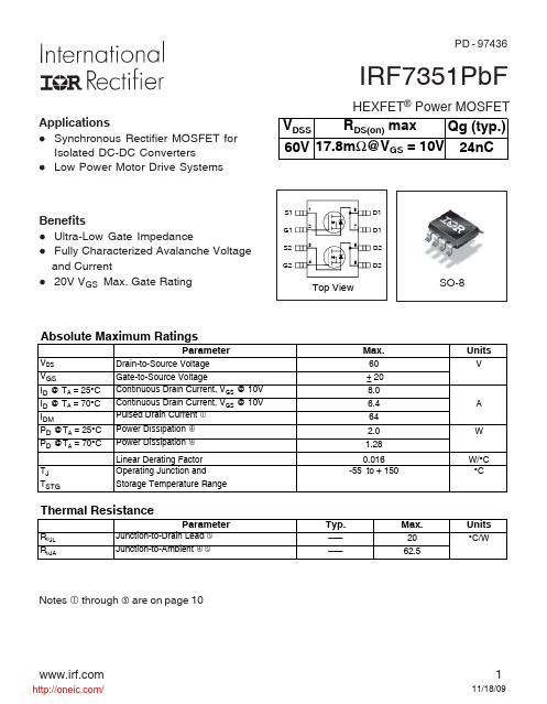
IRF7351TRPBF;IRF7351PBF;中文规格书,Datasheet资料
100
ID, Drain-to-Source Current (A)
10
TJ = 150°C 1
TJ = 25°C
VDS = 25V
≤60µs PULSE WIDTH
0.1
2
3
4
5
6
VGS, Gate-to-Source Voltage (V)
Fig 3. Typical Transfer Characteristics
/
RDS(on) , Drain-to-Source On Resistance (Normalized)
2.0 ID = 8.0A
1.8 VGS = 10V
1.5
1.3
1.0
0.8
0.5 -60 -40 -20 0 20 40 60 80 100 120 140 160 TJ , Junction Temperature (°C)
1
≤60µs PULSE WIDTH Tj = 25°C
0.1 0.1
3.8V
1
10
100
VDS, Drain-to-Source Voltage (V)
1000
ID, Drain-to-Source Current (A)
100 10
TOP BOTTOM
VGS 10V 8.0V 6.0V 5.0V 4.5V 4.3V 4.0V 3.8V
0.2 0.4 0.6 0.8 1.0 1.2 VSD, Source-to-Drain Voltage (V)
Fig 7. Typical Source-Drain Diode Forward Voltage
4
/
10 10msec 1msec
IRLML2244TRPBF;中文规格书,Datasheet资料

1/24/111ORDERING INFORMATION:See detailed ordering and shipping information on the last page of this data sheet.Notes through are on page 10Features and BenefitsBenefitsApplication(s)• System/Load Switchresults in ⇒IRLML2244TRPbFIRLML2244TRPbF 3Fig 2. Typical Output CharacteristicsFig 1. Typical Output CharacteristicsFig 4. Normalized On-ResistanceVs. Temperature-V DS , Drain-to-Source Voltage (V)0.1110100-V DS , Drain-to-Source Voltage (V)-I D , D r a i n -t o -S o u r c e C u r r e n t (A )T J , Junction Temperature (°C)R D S (o n ) , D r a i n -t o -S o u r c e O n R e s i s t a n c eIRLML2244TRPbFFig 6. Typical Gate Charge Vs.Gate-to-Source VoltageFig 5. Typical Capacitance Vs.Drain-to-Source Voltage Fig 8. Maximum Safe Operating AreaFig 7. Typical Source-Drain DiodeForward Voltage110100-V DS , Drain-to-Source Voltage (V)10100100010000C , C a p a c i t a n c e (p F )-V SD , Source-to-Drain Voltage (V)0.1110100-I S D , R e v e r s e D r a i n C u r r e n t (A )110100-V DS , Drain-to-Source Voltage (V)0.010.1110100-I D , D r a i n -t o -S o u r c e C u r r e n t (A)048121620Q G, Total Gate Charge (nC)2468101214-V G S , G a t e -t o -S o u r c e V o l t a g e (V )IRLML2244TRPbF 5Fig 11. Typical Effective Transient Thermal Impedance, Junction-to-AmbientFig 9. Maximum Drain Current Vs.Ambient TemperatureFig 10b. Switching Time WaveformsFig 10a. Switching Time Test Circuit255075100125150T A , Ambient Temperature (°C)012345-I D , D r a i n C u r r e n t (A)t 1 , Rectangular Pulse Duration (sec)R DV DDV DSV t t t tFig 13. Typical On-Resistance Vs. DrainCurrentFig 12. Typical On-Resistance Vs. GateVoltageFig 14b. Gate Charge Test CircuitFig 14a. Basic Gate Charge Waveform 24681012-V GS, Gate -to -Source Voltage (V)20406080100120R D S (o n ), D r a i n -t o -S o u r c e O n R e s i s t a n c e (m Ω)5101520253035-I D , Drain Current (A)04080120160200R D S (o n ), D r a i n -t o -S o u r c e O n R e s i s t a n c e (m Ω)Vgs = -4.5VIdQgs1Qgs2Qgd Qgodr 0 7Fig 15. Typical Threshold Voltage Vs.Junction TemperatureFig 16. Typical Power Vs. TimeT J , Temperature ( °C )-V G S (t h ), G a t e t h r e s h o l d V o l t a g e (V )Time (sec)P o w e r (W )IRLML2244TRPbFMicro3 (SOT-23/TO-236AB) Part Marking InformationMicro3 (SOT-23) Package OutlineDimensions are shown in millimeters (inches)Note: For the most current drawing please refer to IR website at: /package/cF =DA T E C E =X = D =C =B =A =W = (1-26) IF PRECEDED BY LAST DIG IT O F C ALENDA R YEA RH =G =KH G F E D C B 200620032002200520042008200720102009J Y 51292830C B D52ZNote: A line a bove the work we e k(a s s how n he re ) indic a tes Le a d - Fre e.I =J = IRLML2030L = IRLML0060M = IRLML0040K = IRLML0100N = IRLML2060P = IRLML9301R = IRLML9303C u HALOG PAIRLML2244TRPbF 9Micro3™ Tape & Reel InformationDimensions are shown in millimeters (inches)2.05 ( .080 )1.95 ( .077 )TRFEED DIRECTION4.1 ( .161 )3.9 ( .154 )1.6 ( .062 )1.5 ( .060 )1.85 ( .072 )1.65 ( .065 )3.55 ( .139 )3.45 ( .136 )1.1 ( .043 )0.9 ( .036 )4.1 ( .161 )3.9 ( .154 )0.35 ( .013 )0.25 ( .010 )8.3 ( .326 )7.9 ( .312 )1.32 ( .051 )1.12 ( .045 )9.90 ( .390 )8.40 ( .331 )178.00( 7.008 ) MAX.NOTES:1. CONTROLLING DIMENSION : MILLIMETER.2. OUTLINE CONFORMS TO EIA-481 & EIA-541.Note: For the most current drawing please refer to IR website at: /package/IRLML2244TRPbFData and specifications subject to change without notice.IR WORLD HEADQUARTERS: 233 Kansas St., El Segundo, California 90245, USA Tel: (310) 252-7105TAC Fax: (310) 252-7903Visit us at for sales contact information .01/2011Qualification standards can be found at International Rectifier’s web site /product-info/reliabilityHigher qualification ratings may be available should the user have such requirements. Please contact your International Rectifier sales representative for further information: /whoto-call/salesrep/Applicable version of JEDEC standard at the time of product release.Notes:Repetitive rating; pulse width limited by max. junction temperature. Pulse width ≤ 400μs; duty cycle ≤ 2%. Surface mounted on 1 in square Cu board Refer to application note #AN-994.Qualification information †分销商库存信息: IRIRLML2244TRPBF。
IRS2003STRPbF中文资料
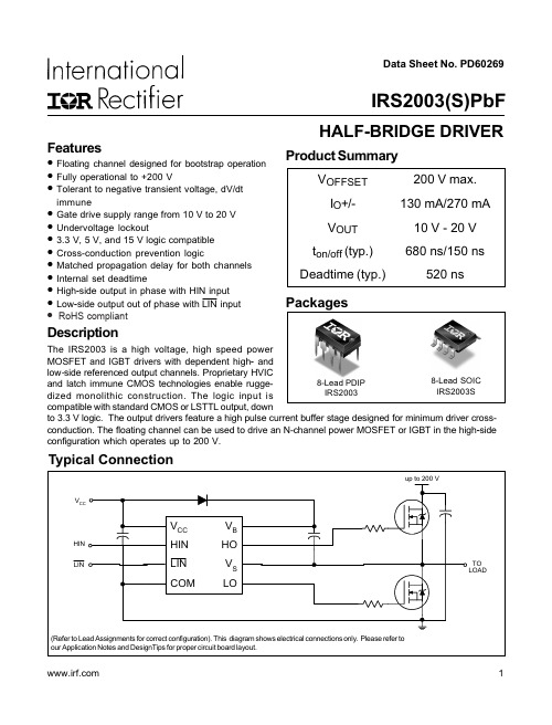
Data Sheet No. PD60269Typical ConnectionProduct SummaryV OFFSET 200 V max.I O +/-130 mA/270 mA V OUT 10 V - 20 V t on/off (typ.)680 ns/150 nsDeadtime (typ.)520 nsHALF-BRIDGE DRIVERFeatures•Floating channel designed for bootstrap operation •Fully operational to +200 V•Tolerant to negative transient voltage, dV/dtimmune•Gate drive supply range from 10 V to 20 V •Undervoltage lockout•3.3 V, 5 V, and 15 V logic compatible •Cross-conduction prevention logic•Matched propagation delay for both channels •Internal set deadtime•High -side output in phase with HIN input •Low -side output out of phase with LIN input DescriptionThe IRS2003 is a high voltage, high speed power MOSFE T and IGBT drivers wi th dependent high - and low -side referenced output channels. Proprietary HVICand latch immune CMOS technologies enable rugge-dized monolithic construction. The logic input iscompatible with standard CMOS or LSTTL output, downto 3.3 V logic. The output drivers feature a high pulse current buffer stage designed for minimum driver cross-conduction. The floating channel can be used to drive an N-channel power MOSFET or IGBT in the high -side configuration which operates up to 200 V. 1IRS2003(S)PbFPackages8-Lead PDIP IRS20038-Lead SOIC IRS2003S • RoHS compliantIRS2003(S)PbFAbsolute Maximum RatingsAbsolute maximum ratings indicate sustained limits beyond which damage to the device may occur. All voltage param-eters are absolute voltages referenced to COM. The thermal resistance and power dissipation ratings are measured under board mounted and still air conditions.Note 1: Logic operational for V S of -5 V to +200 V. Logic state held for V S of -5 V to -V BS . (Please refer to the Design Tip DT97-3 for more details).IRS2003(S)PbFStatic Electrical CharacteristicsV BIAS (V CC, V BS) = 15 V and T A = 25 °C unless otherwise specified. The V IN, V TH, and I IN parameters are referenced to COM. The V O and I O parameters are referenced to COM and are applicable to the respective output leads: HO or LO. Dynamic Electrical CharacteristicsV BIAS (V CC, V BS) = 15 V, C L = 1000 pF and T A = 25 °C unless otherwise specified.IRS2003(S)PbFLead DefinitionsSymbol DescriptionHIN Logic input for high -side gate driver output (HO), in phase Logic input for low-side gate driver output (LO), out of phase V B High -side floating supply HO High -side gate drive output V S High -side floating supply return V CC Low-side and logic fixed supply LO Low -side gate drive output COMLow -side returnLIN Lead Assignments8 Lead PDIP 8 Lead SOICIRS2003PbF IRS2003SPbF12348765V CC HIN LIN COMV B HO V S LO12348765V CC HIN LIN COMV B HO V S LOIRS2003(S)PbFLINHOLOHINFigure 3. Deadtime Waveform DefinitionsFigure 2. Switching Time Waveform DefinitionsLOIRS2003(S)PbFIRS2003(S)PbF8-50-250255075100125Temperature (oC)Figure 10A. Logic "0"(HIN) & Logic "1" ( )Input Voltage vs. TemperatureLINIRS2003(S)PbFIRS2003(S)PbFIRS2003(S)PbF10vs. Temperaturevs. VoltageFigure 17A. Logic "0" Input Bias Currentvs. TemperatureFigure 17B. Logic "0" Input Bias Currentvs. VoltageL o g i c “0” I n p u t B i a s C u r r e n t (µA )0123456-50-250255075100125Temperature (°C)F ig u r e 17A. L o g ic "0" I n p u t B ia s C u r r e n t 0123456101214161820Supply Voltage (V)Case OutlinesCTape & Reel 8-lead SOICPer SCOP 200-002The SOIC-8 is MSL 2 qualified.This product has been designed and qualified for the industrial level.Qualification standards can be found at Data and specifications subject to change without notice. 11/27/2006。
IRF7343QTRPBF;中文规格书,Datasheet资料
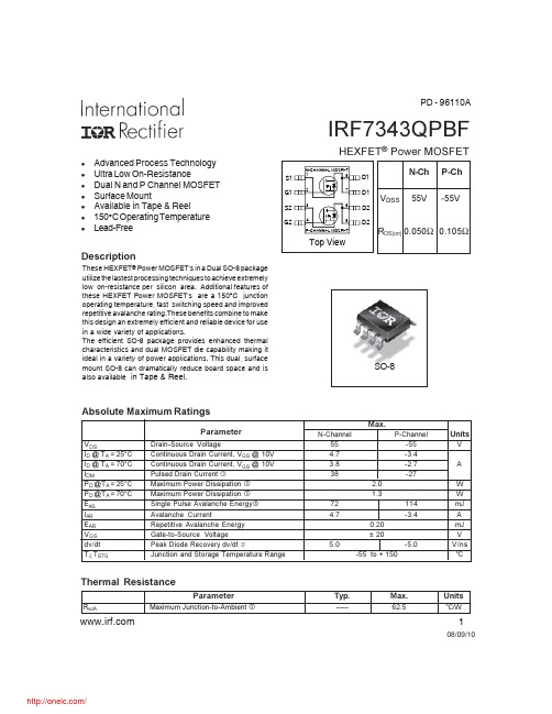
IRF7343QPBF
HEXFET® Power MOSFET
N-CHANNEL MOSFET
S1
1
8
D1
N-Ch P-Ch
G1
2
S2
3
7
D1
VDSS 55V -55V
6
D2
G2
4
5
D2
P-CHANNEL MOSFET
RDS(on) 0.050Ω 0.105Ω
Top View
SO-8
Absolute Maximum Ratings
12V 10V
8.0V 46..50VV 4.0V 3.5V
BOTTOM 3.0V
10
3.0V
20µs PULSE WIDTH
TJ= 25 °C 1
0.1
1
10
100
VDS , Drain-to-Source Voltage (V)
Fig 1. Typical Output Characteristics
Description
These HEXFET® Power MOSFET's in a Dual SO-8 package utilize the lastest processing techniques to achieve extremely low on-resistance per silicon area. Additional features of these HEXFET Power MOSFET's are a 150°C junction operating temperature, fast switching speed and improved repetitive avalanche rating.These benefits combine to make this design an extremely efficient and reliable device for use in a wide variety of applications. The efficient SO-8 package provides enhanced thermal characteristics and dual MOSFET die capability making it ideal in a variety of power applications. This dual, surface mount SO-8 can dramatically reduce board space and is also available in Tape & Reel.
IR3553MTRPBF;中文规格书,Datasheet资料
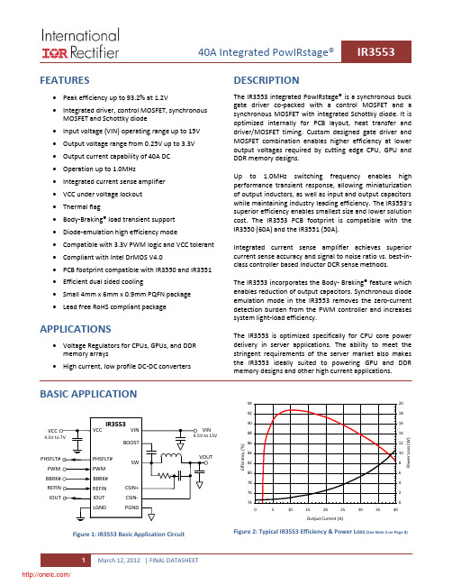
FEATURES∙ Peak efficiency up to 93.2% at 1.2V∙ Integrated driver, control MOSFET, synchronous MOSFET and Schottky diode ∙ Input voltage (VIN) operating range up to 15V ∙ Output voltage range from 0.25V up to 3.3V ∙ Output current capability of 40A DC ∙ Operation up to 1.0MHz∙ Integrated current sense amplifier ∙ VCC under voltage lockout ∙ Thermal flag∙ Body-Braking® load transient support ∙ Diode-emulation high efficiency mode∙ Compatible with 3.3V PWM logic and VCC tolerant ∙ Compliant with Intel DrMOS V4.0∙ PCB footprint compatible with IR3550 and IR3551 ∙ Efficient dual sided cooling∙ Small 4mm x 6mm x 0.9mm PQFN package ∙ Lead free RoHS compliant packageAPPLICATIONS∙ Voltage Regulators for CPUs, GPUs, and DDR memory arrays ∙ High current, low profile DC-DC convertersDESCRIPTIONThe IR3553 integrated PowIRstage® is a synchronous buck gate driver co-packed with a control MOSFET and a synchronous MOSFET with integrated Schottky diode. It is optimized internally for PCB layout, heat transfer and driver/MOSFET timing. Custom designed gate driver and MOSFET combination enables higher efficiency at lower output voltages required by cutting edge CPU, GPU and DDR memory designs.Up to 1.0MHz switching frequency enables high performance transient response, allowing miniaturization of output inductors, as well as input and output capacitors while maintaining industry leading efficiency. The IR3553’s superior efficiency enables smallest size and lower solution cost. The IR3553 PCB footprint is compatible with the IR3550 (60A) and the IR3551 (50A).Integrated current sense amplifier achieves superior current sense accuracy and signal to noise ratio vs. best-in-class controller based Inductor DCR sense methods. The IR3553 incorporates the Body- Braking® feature which enables reduction of output capacitors. Synchronous diode emulation mode in the IR3553 removes the zero-current detection burden from the PWM controller and increases system light-load efficiency.The IR3553 is optimized specifically for CPU core power delivery in server applications. The ability to meet the stringent requirements of the server market also makes the IR3553 ideally suited to powering GPU and DDR memory designs and other high current applications.PINOUT DIAGRAMFigure 3: IR3553 Pin Diagram, Top ViewORDERING INFORMATIONTYPICAL APPLICATION DIAGRAMIOUTVCC BBRK#REFINVOUTFigure 4: Application Circuit with Current Sense AmplifierTYPICAL APPLICATION DIAGRAM (CONTINUED)VCC BBRK#VOUTFigure 5: Application Circuit without Current Sense AmplifierFUNCTIONAL BLOCK DIAGRAMPHSFLT#REFINPWM VIN SWSW SW SW SWSW TGND BOOST IOUT VCCBBRK#GATEL CSIN+LGNDPGNDFigure 6: IR3553 Functional Block DiagramPIN DESCRIPTIONSABSOLUTE MAXIMUM RATINGSStresses beyond those listed under “Absolute Maximum Ratings” may cause permanent damage to the device. These are stress ratings only and functional operation of the device at these or any other conditions beyond those indicated in the operational sections of the specifications are not implied.Note:1. Maximum BOOST – SW = 8V.2. Maximum VIN – SW = 25V.3. All the maximum voltage ratings are referenced to PGND (Pins 12 and 13).Note:1. Thermal Resistance (θJA) is measured with the component mounted on a high effective thermal conductivity test board in free air.Refer to International Rectifier Application Note AN-994 for details.ELECTRICAL SPECIFICATIONSThe electrical characteristics involve the spread of values guaranteed within the recommended operating conditions. Typical values represent the median values, which are related to 25°C.RECOMMENDED OPERATING CONDITIONS FOR RELIABLE OPERATION WITH MARGINELECTRICAL CHARACTERISTICSNotes1. Guaranteed by design but not tested in production2.V IN=12V, V OUT=1.2V, ƒSW = 300kHz, L=210nH (0.2mΩ), VCC=6.8V, C IN=47uF x 4, C OUT =470uF x3, 400LFM airflow, no heat sink, 25°Cambient temperature, and 8-layer PCB of 3.7” (L) x 2.6” (W). PWM controller loss and inductor loss are not included.3. V IN=12V, V OUT=1.2V, ƒSW = 400kHz, L=150nH (0.29mΩ), VCC=7V, C IN=47uF x 4, C OUT =470uF x3, no airflow, no heat sink, 25°C ambienttemperature, and 8-layer PCB of 3.7” (L) x 2.6” (W). PWM controller loss and inductor loss are not included.TYPICAL OPERATING CHARACTERISTICSCircuit of Figure 32, V IN =12V, V OUT =1.2V, ƒSW = 400kHz, L=150nH (0.29m Ω), VCC=7V, T AMBIENT = 25°C, no heat sink, no air flow, 8-layer PCB board of 3.7” (L) x 2.6” (W), no PWM controller loss, no inductor loss, unless specified otherwise.TYPICAL OPERATING CHARACTERISTICS (CONTINUED)Circuit of Figure 32, V IN =12V, V OUT =1.2V, ƒSW = 400kHz, L=150nH (0.29m Ω), VCC=7V, T AMBIENT = 25°C, no heat sink, no air flow, 8-layer PCB board of 3.7” (L) x 2.6” (W), no PWM controller loss, no inductor loss, unless specified otherwise.Figure 13: Normalized Power Loss vs. VCC Voltage Figure 14: Power Loss vs. Output Inductor Figure 15: VCC Current vs. Switching FrequencyFigure 16: Switching Waveform, I OUT = 0AFigure 17: Switching Waveform, I OUT = 40AFigure 18: PWM to SW Delays, I OUT = 10APWM 2V/divSW 5V/div40ns/divPWM 5V/divSW 5V/divGATEL 10V/div400ns/divPWM 5V/divSW 5V/divGATEL 10V/div400ns/div分销商库存信息: IRIR3553MTRPBF。
5713中文资料
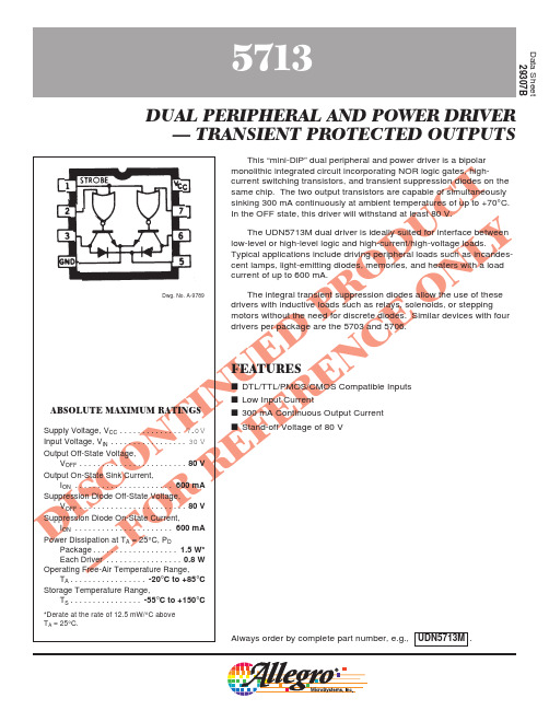
lOFF
VON
ILK VD lCC(1) lCC(0)
— — — — NOM NOM NOM NOM
MIN OPEN
MIN MIN NOM NOM MAX MAX
2.0 V 2.0 V 0.8 V 0.8 V 0V VCC 5.0 V 0V
0V
80 V
—
0V
80 V
—
0.8 V 150 mA —
0.8 V 300 mA —
Suppression Diode On-State Current,
I O ION . . . . . . . . . . . . . . . . . . . . . . 600 mA D F Power Dissipation at TA = 25°C, PD
FEATURES
s DTL/TTL/PMOS/CMOS Compatible Inputs s Low Input Current s 300 mA Continuous Output Current s Stand-off Voltage of 80 V
Storage Temperature Range,
TS . . . . . . . . . . . . . . . . -55°C to +150°C
*Derate at the rate of 12.5 mW/°C above TA = 25°C.
Always order by complete part number, e.g., UDN5713M .
—
— -50 -100 µA
2
IIN(0)
—
MAX 0.4 V 30 V
—
— -100 -200 µA —
IRLML2803TRPBF;中文规格书,Datasheet资料
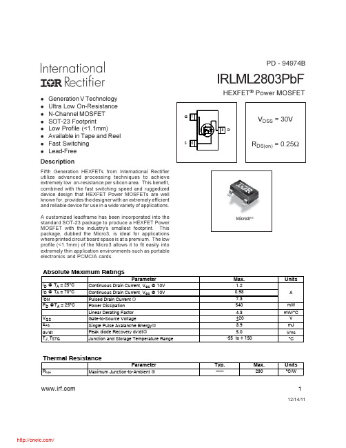
Gate-to-Source Charge
0.48 0.72 nC VDS = 24V
Qgd
Gate-to-Drain ("Miller") Charge
1.1 1.7
VGS = 10V, See Fig. 6 and 9
td(on)
Turn-On Delay Time
3.9
2
/
ID , Drain-to-Source Current (A)
10
VGS
TOP
15V
10V
7.0V
5.5V
4.5V
4.0V
3.5V
BOTTOM 3.0V
1
0.1 0.1
3.0V
20μs PULSE WIDTH
TJ = 25°C
A
1
10
VDS , Drain-to-Source Voltage (V)
A customized leadframe has been incorporated into the standard SOT-23 package to produce a HEXFET Power MOSFET with the industry's smallest footprint. This package, dubbed the Micro3, is ideal for applications where printed circuit board space is at a premium. The low profile (<1.1mm) of the Micro3 allows it to fit easily into extremely thin application environments such as portable electronics and PCMCIA cards.
IR1155STRPBF;IR1155SPBF;中文规格书,Datasheet资料
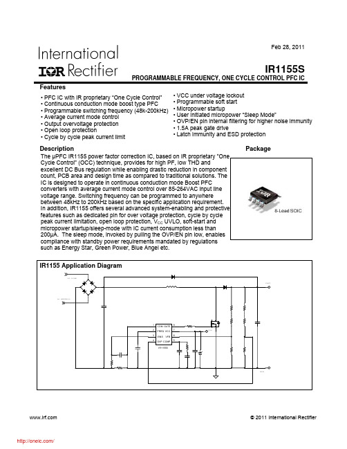
Feb 28, 2011IR1155SPROGRAMMABLE FREQUENCY, ONE CYCLE CONTROL PFC ICFeaturesDescription Package• PFC IC with IR proprietary “One Cycle Control” • Continuous conduction mode boost type PFC • Programmable switching frequency (48k-200kHz) • Average current mode control • Output overvoltage protection • Open loop protection • Cycle by cycle peak current limit • VCC under voltage lockout• Programmable soft start • Micropower startup • User initiated micropower “Sleep Mode”• OVP/EN pin internal filtering for higher noise immunity • 1.5A peak gate drive• Latch immunity and ESD protection The μPFC IR1155 power factor correction IC, based on IR proprietary "OneCycle Control" (OCC) technique, provides for high PF, low THD and excellent DC Bus regulation while enabling drastic reduction in component count, PCB area and design time as compared to traditional solutions. The IC is designed to operate in continuous conduction mode Boost PFC converters with average current mode control over 85-264VAC input line voltage range. Switching frequency can be programmed to anywhere between 48kHz to 200kHz based on the specific application requirement. In addition, IR1155 offers several advanced system-enabling and protective features such as dedicated pin for over voltage protection, cycle by cycle peak current limitation, open loop protection, V CCUVLO, soft-start and micropower startup/sleep-mode with IC current consumption less than 200µA. The sleep mode, invoked by pulling the OVP/EN pin low, enables compliance with standby power requirements mandated by regulations such as Energy Star, Green Power, Blue Angel etc.Qualification InformationIndustrialQualification Level Comments: This family of ICs has passed JEDEC’s Industrialqualification. IR’s Consumer qualification level is granted byextension of the higher Industrial level.Moisture Sensitivity LevelMSL2 260°C(per IPC/JEDEC J-STD-020)Machine ModelClass A(per JEDEC standard JESD22-A115)ESDHuman Body ModelClass 1B (passes 500V)(per EIA/JEDEC standard EIA/JESD22-A114)IC Latch-Up Test Class I, Level A (per JESD78)RoHS Compliant YesAbsolute Maximum RatingsParameter Symbol Min. Max. Units RemarksVCC Voltage V CC -0.3 20 VFREQ Voltage V FREQ -0.3 6.5 VISNS Voltage V ISNS -10 0.3 VVFB, OVP Voltage V FB, V OVP -0.3 6.5 VCOMP Voltage V COMP -0.3 6.5 VGATE Voltage V GATE -0.3 18 VISNS Current I ISNS -2 2 mAJunction Temperature T J -40 150 °CStorage Temperature T S -55 150 °CThermal ResistanceJunction to AmbientRθJA128 °C/WPackage Power Dissipation P D976 mWT AMB = 25°CRecommended Operating ConditionsRecommended operating conditions for reliable operation with marginParameter SymbolMin.Typ.Max.UnitsRemarks Supply Voltage V CC12 19 VJunction Temperature T J -25 125 °CSwitching Frequency F SW 48 200 kHzElectrical CharacteristicsThe electrical characteristics involve the spread of values guaranteed within the specified supply voltage and junction temperature range T J from –25 °C to 125°C. Typical values represent the median values, which are related to 25°C. If not otherwise stated, a supply voltage of V CC =15V is assumed for test condition . Supply SectionParameter Symbol Min. Typ. Max. Units Remarks VCC Turn On ThresholdV CC ON 10.65 11.3 11.95 V VCC Turn OffThreshold (Under Voltage Lock Out) V CC UVLO 9.2 9.8 10.4 V VCC Turn On/Off Hysteresis V CC HYST 1.5VOperating CurrentI CC 10 13 mA C load =1nF, F SW =181kHz6 8 mAStandby Mode (Inactive Gate, Inactive Internal Oscillator)V FB <V OLPSee State Transition Diagram Startup CurrentI CCSTART175 uA V CC =V CC ON - 0.1VSleep CurrentI SLEEP 125 200 uASleep Mode (Inactive Gate,Inactive Oscillator)- V OVP <V SLEEP,OFFSee State Transition Diagram Sleep ModeThreshold (Enable)V SLEEP,ON0.80 0.90 1.00 VIC Enable threshold,Bias on OVP pinSleep ModeThreshold (Disable)V SLEEP,OFF 0.53 0.60 0.67VIC Disable threshold, Bias on OVP pinOscillator SectionParameter SymbolMin.Typ.Max.UnitsRemarks Switching Frequency F SW 48 200kHz200khz:C=430pFapprox.48kHz: C=2nF approx. Oscillator Charge Current I OSC(CHG)200 µAOscillator DischargeCurrentI OSC(DCHG) 6.6 mAOscillator Peak V OSC PK 4 VOscillator Valley V OSC VAL 2 V5 %C=2nF,T A = 25°CInitial Accuracy F SW ACC8 %C=500pF,T A = 25°C Voltage Stability V STAB 0.2 1 % 14V < V CC < 19V Temperature Stability T STAB 2 %-25°C≤ T J≤ 125°CTotal Variation F VT 10 %Line&Temperature Maximum Duty Cycle D MAX94 99 %Minimum Duty Cycle D MIN0 %PulseSkippingProtection SectionParameter SymbolMin.Typ.Max.UnitsRemarksOpen Loop Protection (OLP) V FB Threshold V OLP 17 19 21 %V REF Bias on VFB pinOutput Over Voltage Protection (OVP) V OVP 104.5 106.5 108.5 %V REF Bias on OVP/EN pinOutput Over Voltage Protection (OVP) Reset V OVP(RST) 100.2 102.2 104.2 %V REF Bias on OVP/EN pinPeak Current LimitProtection (IPK LMT) I SNSVoltage ThresholdV ISNS-0.85 -0.77 -0.69 V Bias on ISNS pin OVP Input Bias Current I OVP(Bias)-0.2 µAInternal Voltage Reference SectionVoltage Error Amplifier SectionParameter Symbol Min. Typ. Max. Units Remarks Transconductance g m 35 50 65 µS 30 44 58 T AMB = 25°C Source CurrentI OVEA(SRC)20 44 90µA -25°C ≤T AMB ≤ 125°C -57 -43 -30 T AMB = 25°C Sink Current I OVEA(SNK)-90 -43 -20µA -25°C ≤T AMB ≤ 125°CSoft Start Delay Time t SS35 msec R GAIN = 1k Ω, C ZERO = 0.33uF,C POLE = 0.01uF V COMP Voltage (Fault) V COMP FLT 1 1.4 V@ 100µA steady statecurrentEffective V COMP Voltage V COMP EFF 4.6 4.9 5.2 V VFB Input Bias Current I IB(Bias)-0.2 µA V FB =4.9VOutput Low Voltage V OL 0.25 V Output High Voltage V OH 5 5.4 V V COMP Start Voltage V COMP START240 340 460 mVParameter Symbol Min. Typ. Max. Units Remarks Reference Voltage V REF 4.9 5 5.1 V T A = 25°C Line Regulation R REG1020mV14 V < V CC < 19V Temp Stability T STAB 0.4 % -25°C ≤ T AMB ≤ 125°C Total VariationΔV TOT4.855.1VLine & TemperatureCurrent Amplifier SectionUnitsRemarksMax.Parameter SymbolMin.Typ.DC Gain g DC 3.1 V/VCorner Frequency f C 5 kHz - Average current mode, Note 1Note1Input Offset Voltage V IO 4 16 mVI SNS Bias Current I ISNS(Bias) -57 -13 µABlanking Time T BLANK220 370 520 nsGate Driver SectionUnitsMax.Remarks Parameter SymbolMin.Typ.Gate Low Voltage V GLO 0.8 VI GATE=200mAclamp12 13 14 VGateInternalGate High Voltage V GTHV CC = 11.5V10 VRise Time t r20 nsC LOAD = 1nFFall Time t f20 nsC LOAD = 1nFC LOAD = 10nF, Note 1Output Peak Current I OPK 1.5 AGate Voltage @ Fault V G fault 0.08I GATE = 20mAVNote 1 – Guaranteed by design, but Not tested in productionLead Assignments & DefinitionsBlock DiagramVFBCOMPOVPNote: Soft-Start & Normal modes are essentially the same (differentiation above is for purpose of clarity only)VCC Undervoltage LockoutV o l t a g e o n V C C p i nTiming DiagramsOutput Protection分销商库存信息:IRIR1155STRPBF IR1155SPBF。
IRS2101STRPBF中文资料
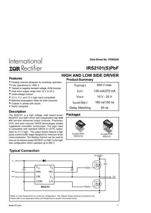
2
元器件交易网
IRS2101(S)PbF
Dynamic Electrical Characteristics
VBIAS (VCC, VBS) = 15 V, CL = 1000 pF and TA = 25 °C unless otherwise specified.
50 1.0 0.625 125 200 150 150 300
Units
V
V/ns W
°C/W °C
Recommended Operating Conditions
The input/output logic timing diagram is shown in Fig. 1. For proper operation the device should be used within the recommended conditions. The VS offset rating is tested with all supplies biased at a 15 V differential.
Package power dissipation @ TA ≤ +25 °C
Thermal resistance, junction to ambient
Junction temperature Storage temperature Lead temperature (soldering, 10 seconds)
V
— 0.05 0.2
IO = 2 mA
— 0.02 0.1
—
—
50
VB = VS = 600 V
—
30 55
— 150 270 µA
VIN = 0 V or 5 V
IR2153STRPBF中文资料
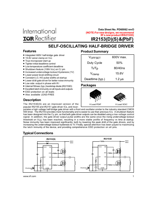
Features••15.6V zener clamp on Vcc •True micropower start up•Tighter initial deadtime control••••Lower power level-shifting circuit•••Low side output in phase with R T•••ESD protection on all leads •Also available LEAD-FREE(NOTE:For new designs, we recommendIR’s new product IRS2153D)SELF-OSCILLATING HALF-BRIDGE DRIVERProduct SummaryTypical ConnectionsIR2153(D)(S) &(PbF)Descriptionporates a high voltage half-bridge gate driver with a front end oscillator similar to the industry standard CMOS 555 timer. The IR2153 provides more functionality and is easier to use than previous ICs. A shutdown feature has been designed into the C T pin, so that both gate driver outputs can be disabled using a low voltage control signal. In addition, the gate driver output pulse widths are the same once the rising undervoltage lockout threshold on V CC has been reached, resulting in a more stable profile of frequency vs time at startup.Noise immunity has been improved significantly, both by lowering the peak di/dt of the gate drivers, and by increasing the undervoltage lockout hysteresis to 1V. Finally, special attention has been payed to maximizing the latch immunity of the device, and providing comprehensive ESD protection on all pins. 1IR2153(D)(S) & (PbF)2NOTE:For new designs, we recommend IR’s new product IRS2153DNote 1:This IC contains a zener clamp structure between the chip V CC and COM which has a nominal breakdown voltage of 15.6V. Please note that this supply pin should not be driven by a DC, low impedance power source greater than the V CLAMP specified in the Electrical Characteristics section.Note 2:Care should be taken to avoid output switching conditions where the V S node flies inductively below ground by more than 5V.Note 3:Enough current should be supplied to the V CC pin of the IC to keep the internal 15.6V zener diode clamping the voltage at this pin.Recommended Operating ConditionsFor proper operation the device should be used within the recommended conditions.Absolute Maximum RatingsAbsolute maximum ratings indicate sustained limits beyond which damage to the device may occur. All voltage param-eters are absolute voltages referenced to COM, all currents are defined positive into any lead. The thermal resistance and power dissipation ratings are measured under board mounted and still air conditions.IR2153(D)(S) & (PbF)3Symbol ComponentMin.Max.UnitsR T Timing resistor value 10— k ΩC TC T pin capacitor value330—pFRecommended Component ValuesIR2153(D)(S) & (PbF)4NOTE:For new designs, we recommend IR’s new product IRS2153DElectrical CharacteristicsV BIAS (V CC , V BS ) = 12V, C L = 1000 pF, C T = 1 nF and T A = 25°C unless otherwise specified. The V IN , V TH and I INparameters are referenced to COM. The V O and I O parameters are referenced to COM and are applicable to the respective output leads: HO or LO.IR2153(D)(S) & (PbF)5SymbolDescriptionV CC Logic and internal gate drive supply voltage R T Oscillator timing resistor input C T Oscillator timing capacitor input COM IC power and signal ground LO Low side gate driver outputV S High voltage floating supply return HO High side gate driver outputV BHigh side gate driver floating supplyLead Definitions8 Lead PDIP 8 Lead SOICIR2153DIR2153(S)NOTE: The IR2153D is offered in 8 lead PDIP only.Electrical Characteristics (cont.)IR2153(D)(S) & (PbF) 6NOTE:For new designs, we recommendIR’s new product IRS2153DFunctional Block Diagram for IR2153(S) Functional Block Diagram for IR2153DIR2153(D)(S) & (PbF)8NOTE:For new designs, we recommend IR’s new product IRS2153DFigure 1. Input/Output Timing DiagramFigure 3. Deadtime Waveform DefinitionsR TTCLAMPR T Figure 2. Switching Time Waveform Definitions(HO)(LO)IR2153(D)(S) & (PbF)9Per SCOP 200-002。
IR1153STRPBF;IR1153SPBF;中文规格书,Datasheet资料
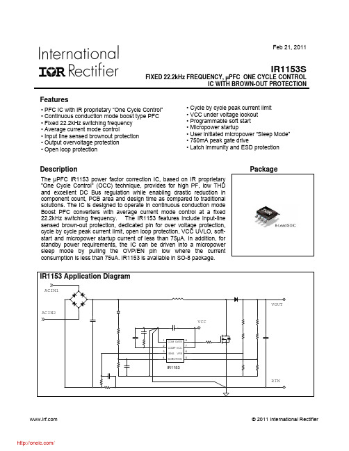
Feb 21, 2011IR1153SFIXED 22.2kHz FREQUENCY, µPFC ONE CYCLE CONTROLIC WITH BROWN-OUT PROTECTIONFeaturesDescription Package• PFC IC with IR proprietary “One Cycle Control” • Continuous conduction mode boost type PFC • Fixed 22.2kHz switching frequency • Average current mode control • Input line sensed brownout protection • Output overvoltage protection • Open loop protection • Cycle by cycle peak current limit• VCC under voltage lockout • Programmable soft start • Micropower startup • User initiated micropower “Sleep Mode” • 750mA peak gate drive• Latch immunity and ESD protection The μPFC IR1153 power factor correction IC, based on IR proprietary"One Cycle Control" (OCC) technique, provides for high PF, low THD and excellent DC Bus regulation while enabling drastic reduction incomponent count, PCB area and design time as compared to traditional solutions. The IC is designed to operate in continuous conduction mode Boost PFC converters with average current mode control at a fixed 22.2kHz switching frequency. The IR1153 features include input-line sensed brown-out protection, dedicated pin for over voltage protection, cycle by cycle peak current limit, open loop protection, VCC UVLO, soft-start and micropower startup current of less than 75µA. In addition, for standby power requirements, the IC can be driven into a micropower sleep mode by pulling the OVP/EN pin low where the current consumption is less than 75uA. IR1153 is available in SO-8 package.Qualification InformationIndustrialQualification Level Comments: This family of ICs has passed JEDEC’s Industrial qualification.IR’s Consumer qualification level is granted by extension of the higherIndustrial level.Moisture Sensitivity LevelMSL2 260°C(per IPC/JEDEC J-STD-020)Machine ModelClass A(per JEDEC standard JESD22-A115)ESDHuman Body ModelClass 1A(per EIA/JEDEC standard EIA/JESD22-A114)IC Latch-Up Test Class I, Level A (per JESD78)RoHS Compliant YesAbsolute Maximum RatingsStresses beyond those listed under “Absolute Maximum Ratings” may cause permanent damage to the device. These are stress ratings only and functional operation of the device at these conditions is not implied. All voltages are absolute voltages referenced to COM. Thermal resistance and power dissipation are measured under board mounted and still air conditions.Parameters Symbol Min.Max.Units Remarks V CC Voltage V CC-0.3 20 V Not internally clampedISNS voltage V ISNS -10 0.3 VISNS Current I ISNS -2 2 mAV FB voltage V FB-0.3 6.5 VV OVP voltage V OVP -0.3 6.5 VV BOP voltage V BOP -0.3 9 VCOMP voltage V COMP -0.3 6.5 VGate Voltage V GATE-0.3 18 VJunction Temperature OperatingRange T J -40 150 °CStorage Temperature T S -55 150 °CThermal Resistance RθJA128 °C/WSOIC-8Package Power Dissipation P D 976 mWT AMB=25°C SOIC-8Electrical CharacteristicsThe electrical characteristics involve the spread of values guaranteed within the specified supply voltage and junction temperature range T J from – 25° C to 125°C. Typical values represent the median values, which are related to 25°C. If not otherwise stated, a supply voltage of V CC =15V is assumed for test condition.Supply SectionParameters SymbolMin.Typ.Max.Units Remarks Supply Voltage OperatingRangeV CC14 17 VV CC Turn On Threshold V CC ON 12.2 13.1 14 VV CC Turn Off Threshold(Under Voltage Lock Out)V CC UVLO 9.4 10.1 10.8 VV CC Turn On/Off Hysteresis V CC HYST 2.4 3 3.6 V7 mA C LOAD =1nF8 mA C LOAD =4.7nFOperating Current I CC3.5 5 mA OVP Mode, Inactive gateStart-up Current I CC START26 75 µA V CC=V CC ON - 0.2VSleep current I SLEEP 26 75 µAPinOVP/EN=V SLEEP-0.2VSleep Mode Threshold V SLEEP0.5 0.8 V Bias on OVP/EN pinOscillator SectionParameters SymbolMin.Typ.Max.Units Remarks20.2 22.2 24.2 T AMB=25°CFixed Oscillator Frequency f SW18.3 25 kHz -25°C < T AMB < 125°CMaximum Duty Cycle D MAX9399 % V COMP=5VMinimum Duty Cycle D MIN0 % Pulse SkippingProtection SectionParameters SymbolMin.Typ.Max.Units RemarksOpen Loop Protection (OLP)Threshold V OLP 17 19 21%V REFBias on VFB pinOutput OvervoltageProtection (OVP) Threshold V OVP 104 106 108%V REFBias on OVP/EN pinOutput Overvoltage Protection Reset Threshold V OVP(RST) 101 103 105%V REFBias on OVP/EN pinOVP Input Bias Current I OVP(Bias)-0.2 µABrown-out Protection(BOP) ThresholdV BOP0.66 0.76 0.86 V Bias on BOP pin Brown-out ProtectionEnable ThresholdV BOP(EN) 1.46 1.56 1.66 V Bias on BOP pin BOP Input Bias Current I BOP(Bias)-0.2 µAPeak Current LimitProtection ISNS Voltage Threshold (IPK LIMIT) V ISNS(PK)-0.58 -0.51 -0.44 V Bias on ISNS pinInternal Voltage Reference SectionParameters Symbol Min. Typ. Max. Units RemarksReference Voltage V REF 4.9 5 5.1 V Regulation Voltage on VFB pin,T AMB =25°C Line Regulation R REG 10 20 mV 14V < V CC < 17VTemp Stability T STAB0.4 % -25°C < T AMB < 125°C, Note 1 Total VariationΔV TOT4.835.12 V Line & TemperatureVoltage Error Amplifier SectionParameters Symbol Min. Typ. Max. Units RemarksTransconductance g m 35 49 59 µS30 44 58 T AMB =25°C Source Current (Normal Mode) I OVEA(SRC)17 80 µA-25°C < T AMB < 125°C-58 -44 -30 T AMB =25°CSink Current (Normal Mode) I OVEA(SNK)-80 -17 µA -25°C < T AMB < 125°C Soft Start Delay Time (calculated) t SS 35 msecR GAIN =8k Ω, C ZERO =0.33μF,C POLE =2nF V COMP Voltage (Fault) V COMP FLT 1 1.5 V @100uA steady stateEffective V COMP voltageV COMP EFF 4.7 4.9 5.1 VVFB Input Bias Current I FB(Bias) -0.2 µAOutput Low Voltage V OL 0.25 VOutput High Voltage V OH 5 5.45 VV COMP Start VoltageV COMP START210 325 435 mVCurrent Amplifier SectionMax.Units RemarksTyp.Min.Parameters SymbolDC Gain g DC 5.65 V/V2 kHz Average Current Mode, Note 1 Corner Frequency fCInput Offset Voltage V IO 4 16 mV Note 1ISNS Input Bias Current I ISNS(Bias)-57-13 µA170 320 470 nsBlanking Time TBLANKGate Driver SectionMax.Units Remarks Parameters SymbolMin.Typ.Gate Low Voltage V GLO 0.8 V I GATE = 200mA13.1 14.1 15.1 V CC=17V, Internally Clamped Gate High Voltage V GTH9.5 V V CC=11.5VnsC LOAD = 1nF, VCC=15V25Rise Time t rC LOAD = 4.7nF, VCC=15Vns6035C LOAD = 1nF, VCC=15VnsFall Time t fC LOAD = 4.7nF, VCC=15Vns65Output Peak Current I OPK750 mA C LOAD = 4.7nF, VCC=15V, Note 1 Gate Voltage at Fault V G fault0.08 V I GATE = 20mANote 1: Guaranteed by design, but not tested in productionBlock DiagramLead Assignments & DefinitionsIRS1144IR1153IR1144SIR1153 General DescriptionThe μPFC IR1153 IC is intended for power factor correction in continuous conduction mode Boost PFC converters operating at fixed switching frequency with average current mode control. The IC operates based on IR's proprietary "One Cycle Control" (OCC) PFC algorithm based on the concept of resettable integrator.Theory of OperationThe OCC algorithm based on the resettable integrator concept works using two loops - a slow outer voltage loop and a fast inner current loop. The outer voltage loop monitors the VFB pin and generates an error signal which controls the amplitude of the input current admitted into the PFC converter. In this way, the outer voltage loop maintains output voltage regulation. The voltage loop bandwidth is kept low enough to not track the 2xf AC ripple in the output voltage and thus generates an almost DC error signal under steady state conditions.The inner current loop maintains the sinusoidal profile of the input current and thus is responsible for power factor correction. The information about the sinusoidal variation in input voltage is inherently available in the input line current (or boost inductor current). Thus there is no need to sense the input voltage to generate a current reference. The current loop employs the boost inductor current information to generate PWM signals with a proportional sinusoidal variation. This controls the shape of the input current to be proportional to and in phase with the input voltage. Average current mode operation is envisaged by filtering the switching frequency ripple from the current sense signal using an appropriately sized on-chip RC filter. This filter also contributes to the bandwidth of the current control loop. Thus the filter bandwidth has to be high enough to track the 120Hz rectified, sinusoidal current waveform and also filter out the switching frequency ripple in the inductor current. In IR1153 this averaging function can effectively filter high ripple current ratios (as high as 40% at maximum input current) to accommodate designs with small boost inductances.The IC determines the boost converter instantaneous duty cycle based on the resettable integrator concept. The required signals are the voltage feedback loop error signal V m (which is the V COMP pin voltage minus a DC offset of V COMP,START) and the current sense signal V ISNS. The resettable integrator generates a cycle-by-cycle, saw-tooth signal called the PWM Ramp which has an amplitude V m and period 1/f SW hence a slope of V m*f SW. The current sense signal is amplified by the current amplifier by a factor g DC and fed into the summing node where it is subtracted from V m to generate the summer voltage (= V m–g DC*V ISNS). The summer voltage is compared with the PWM ramp by the PWM comparator of the IC to determine the gate drive duty cycle. The instantaneous duty is mathematically given by:D = (V m - g DC.V ISNS)/V mAssuming steady state condition where the voltage feedback loop is well regulated (V m & V OUT are DC signals) & hence instantaneous duty cycle follows the boost-converter equation (D = 1 – V IN(t)/V OUT), the control equation can be re-written as:V m = g DC.V ISNS/(V IN(t)/V OUT)Further, recognizing that V ISNS = I L(t).R SNS and re-arranging yields:g DC.I L(t).R SNS = V m V IN(t)/V OUTSince V m, V OUT & g DC are constant terms:I L(t) α V IN(t)Thus the inductor current follows the input voltage waveform & by definition power factor correction is achieved.Feature setFixed Frequency OperationThe IC is programmed to operate at a fixed frequency of 22.2kHz (Typ). Internalization of the oscillator offers excellent noise immunity even in the noisy PFC environment while integration of the oscillator into the OCC core of the IC eliminates need for digital calibration circuits. Both these factors render the gate drive jitter free thus contributing to elimination of audible noise in PFC magnetics.IC Supply Circuit & Low start-up currentThe IR1153 UVLO circuit maintains the IC in UVLO mode during start-up if VCC pin voltage is less than the VCC turn-on threshold, V CC,ON and current consumption is less than 75uA. Should VCC pin voltage should drop below V CC,UVLO during normal operation, the IC is pushed back into UVLO mode and VCC pin has to exceed V CC,ON again for normal operation. There is no internal voltage clamping of the VCC pin.User initiated Micropower Sleep modeThe IC can be actively pushed into a micropower Sleep Mode where current consumption is less than 75uA by pulling OVP/EN pin below the Sleep threshold, V SLEEP even while VCC is above V CC,ON. This allows the user to disable PFC during application stand-by situations in order to meet stand-by regulations. Since V SLEEP is less than 1V, even logic level signals can be employed.IR1153SIR1153 General DescriptionProgrammable Soft StartThe soft start process controls the rate of rise of the voltage feedback loop error signal thus providing a linear increase of the RMS input current that the PFC converter will admit. The soft start time is essentially controlled by voltage error amplifier compensation components selected and is therefore user programmable to some degree based on desired voltage feedback loop crossover frequency.Gate Drive CapabilityThe gate drive output stage of the IC is a totem pole driver with 750mA peak current drive capability. The gate drive is internally clamped at 14.1V (Typ). Gate drive buffer circuits (especially cost-effective base-followers) can be easily driven with the GATE pin of the IC to suit any system power level.System Protection FeaturesIR1153 protection features include Brown-out protection (BOP), Open-loop protection (OLP), Overvoltage protection (OVP), Cycle-by-cycle peak current limit (IPK LIMIT), Soft-current limit and VCC under voltage lock-out (UVLO).- BOP is based on direct input line sensing using a resistor divider/RC filter network. If BOP pin falls below the Brown-out protection threshold V BOP, a Brown-out situation is immediately detected the following response is executed - the gate drive pulse is disabled, VCOMP is actively discharged and IC is pushed into Stand-by Mode. The IC re-enters normal operation only after BOP pin exceeds V BOP(EN). During start-up the IC is held in Stand-by Mode until this pin exceeds V BOP(EN).- OLP is activated whenever the VFB pin voltage falls below V OLP threshold. Once open loop is detected the following response is immediately executed - the gate drive is immediately disabled, VCOMP is actively discharged and the IC is pushed into Stand-by mode. There is no voltage hysteresis associated with this feature. During start-up the IC is held in Stand-by Mode until VFB exceeds V OLP. - The OVP pin is a dedicated pin for overvoltage protection that safeguards the system even if there is a break in the VFB feedback loop due to resistor divider failure etc. An overvoltage fault is triggered when OVP pin voltage exceeds the V OVP threshold of 106%VREF. The response of the IC is to immediately terminate the gate drive output and hold it in that state. The gate drive is re-enabled only after OVP pin voltage drops below V OVP(RST) threshold of 103% VREF. The exact voltage level at which overvoltage protection is triggered can be programmed by the user by carefully designing the OVP pin resistor divider. Itis recommended NOT to set the OVP voltage trigger limit less than 106% of DC bus voltage, since this can endanger the situation where the OVP reset limit will be less than the DC bus voltage regulation point – in this condition the voltage loop can become unstable.- Soft-current limit is an output voltage fold-back type protection feature encountered when the PFC converter input current exceeds to a point where the V m voltage saturates. As mentioned earlier, the amplitude of input current is directly proportional to V m, the error voltage of the feedback loop. V m is clamped to a certain maximum voltage inside the IC (given by V COMP,EFF parameter in datasheet). If the input current causes the V m voltage to saturate at its maximum value, then any further increase in input current will cause the duty cycle to droop which immediately forces the V OUT voltage of the PFC converter to fold-back. Since the highest current is at the peak of the AC sinusoid, the droop in duty cycle commences at the peak of the AC sinusoid when the soft-current limit is encountered. In most converters, the design of the current sense resistor is performed based on soft-current limit (i.e. V m saturation) and at the system condition which demands highest input current (minimum V AC & maximum P OUT).- Cycle-by-cycle peak current limit protection instantaneously turns-off the gate output whenever the ISNS pin voltage exceeds V ISNS(PK) threshold in magnitude. The gate drive is held in the low state as long as the overcurrent condition persists. The gate drive is re-enabled when the magnitude of ISNS pin voltage falls below the V ISNS(PK) threshold. This protection feature incorporates a leading edge blanking circuit to improve noise immunity.IR1153S IR1153 Pin DescriptionPin COM: This is ground potential pin of the IC. All internal devices are referenced to this point. Pin COMP: External circuitry from this pin to ground compensates the system voltage loop and programs the soft start time. The COMP pin is essentially the output of the voltage error amplifier. The voltage loop error signal V m used in the control algorithm is derived from V COMP (V m =V COMP–V COMP,START). V COMP is actively discharged using an internal resistance to below V COMP,START threshold whenever the IC is pushed into Stand-by mode (BOP or OLP condition) or UVLO/Sleep mode. The gate drive output and logic functions of the IC are inactive if VCOMP is less than V COMP,START. Also during start-up, the VCOMP voltage has to be less than V COMP,START in order to commence operation (i.e. a pre-bias on VCOMP will not allow IC to commence operation).Pin ISNS: ISNS pin is tied to the input of the current sense amplifier of the IC. The voltage at this pin, which provides the current sense information to the IC, has to be a negative voltage wrt the COM pin. Also since the IC is based on average current mode, the entire inductor current information is necessary. A current sense resistor, located below system ground along the return path to the bridge rectifier, is the preferred current sensing method. ISNS pin is also the inverting input to the cycle-by-cycle peak current limit comparator. Whenever V ISNS exceeds V ISNS(PK) threshold in magnitude, the gate drive is instantaneously disabled. Any external filtering of the ISNS pin must be performed carefully in order to ensure that the integrity of the current sense signal is maintained for cycle-by-cycle peak current limit protection.Pin BOP (Brown-out Protection): This pin is used to sense the rectified AC input line voltage through a resistor divider/capacitor network which is in effect a voltage division and averaging network, representing a scaled down signal of the average rectified input voltage (average DC voltage + 2xf AC ripple). During start-up the BOP pin voltage has to exceed V BOP(EN) in order to enable the IC to exit Stand-by mode and enter normal operation. A Brown-out situation is detected whenever the pin voltage falls below V BOP and the IC is pushed into Stand-by mode. Subsequently the pin has to exceed V BOP(EN) for the IC to exit Stand-by and resume normal operation.Pin OVP/EN: The OVP/EN pin is connected to the non-inverting input of the OVP(OVP) overvoltage comparator shown in the block diagram and thus is used to detect output overvoltage situations. The output voltage information is communicated to the OVP pin using a resistive divider. This pin also serves the second purpose of an ENABLE pin. The OVP/EN pin can be used to activate the IC into “micropower sleep” mode by pulling the voltage on this pin below the V SLEEP threshold.Pin VFB: The converter output voltage is sensed via a resistive divider and fed into this pin. VFB pin is the inverting input of the output voltage error amplifier. The non-inverting input of this amplifier is connected to an internal 5V reference. The impedance of the divider string must be low enough that it does not introduce substantial error due to the input bias currents of the amplifier, yet high enough to minimize power dissipation. Typical value of external divider total impedance will be around 2MΩ. VFB pin is also the inverting input to the Open Loop comparator. The IC is held in Stand-by Mode whenever VFB pin voltage is below V OLP threshold.Pin VCC: This is the supply voltage pin of the IC and sense node for the undervoltage lock out circuit. It is possible to turn off the IC by pulling this pin below the minimum turn off threshold voltage, V CC(UVLO) without damage to the IC. This pin is not internally clamped.Pin GATE: This is the gate drive output of the IC. It provides a drive current of ±0.75A peak with matched rise and fall times. The gate drive output of the IC is clamped at 14.1V(Typ).分销商库存信息:IRIR1153STRPBF IR1153SPBF。
SQT-103-01-F-D;SQT-106-01-LM-D;SQT-110-03-F-D;SQT-120-01-F-S;中文规格书,Datasheet资料
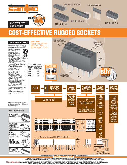
SPECIFICATIONS
For complete specifications see ?SQT
Mates with: TMMH, TMM, MTMM, MMT, TW, LTMM, ZLTMM, ESQT, TCMD
Choice of one through six rows
SQT-106-01-LM-D SQT-112-01-F-D SQT-110-01-L-Q
SQT-110-03-F-D SQT-107-01-L-T SQT-125-01-F-D
(2,29) .050 .090
(2,00) .0787
–RA OPTION
(–Q, –5 & –6 not available)
/
分销商库存信息:
SAMTEC SQT-103-01-F-D SQT-120-01-F-S SQT-110-01-LM-Q SQT-116-01-S-D
TMM/ SQT TMMH
HORIZONTAL
(2,00mm) .0787" pitch
1
NO. PINS PER ROW
LEAD STYLE
(6,35mm) .250"
PLATING OPTION
ROW OPTION
Note: Some lengths, styles and options are non-standard, non-returnable.
20°C
5.5A
(2,62mm) .103" to (5,03mm) .198" Insertion Force: (Single contact only)
40°C
5A
60°C
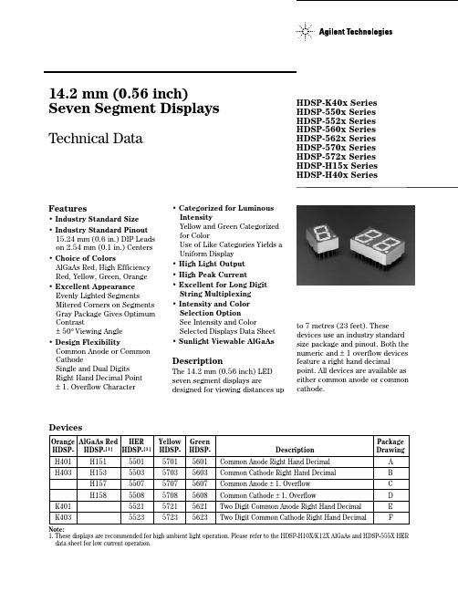
5082-5703-EF000中文资料
14.2 mm (0.56 inch)Seven Segment Displays Technical DataFeatures• Industry Standard Size • Industry Standard Pinout 15.24 mm (0.6 in.) DIP Leads on 2.54 mm (0.1 in.) Centers • Choice of ColorsAlGaAs Red, High Efficiency Red, Yellow, Green, Orange • Excellent Appearance Evenly Lighted Segments Mitered Corners on Segments Gray Package Gives Optimum Contrast±50° Viewing Angle • Design FlexibilityCommon Anode or Common CathodeSingle and Dual Digits Right Hand Decimal Point ±1. Overflow Character• Categorized for Luminous IntensityYellow and Green Categorized for ColorUse of Like Categories Yields a Uniform Display • High Light Output • High Peak Current• Excellent for Long Digit String Multiplexing • Intensity and Color Selection OptionSee Intensity and ColorSelected Displays Data Sheet • Sunlight Viewable AlGaAsDescriptionThe 14.2 mm (0.56 inch) LED seven segment displays aredesigned for viewing distances upto 7 metres (23 feet). Thesedevices use an industry standard size package and pinout. Both the numeric and ±1 overflow devices feature a right hand decimalpoint. All devices are available as either common anode or common cathode.Orange AlGaAs Red HERYellowGreen Package HDSP-HDSP-[1]HDSP-[1]HDSP-HDSP- DescriptionDrawingH401H151550157015601Common Anode Right Hand Decimal A H403H153550357035603Common Cathode Right Hand Decimal B H157550757075607Common Anode ±1. Overflow C H158550857085608Common Cathode ±1. OverflowD K401552157215621Two Digit Common Anode Right Hand DecimalE K403552357235623Two Digit Common Cathode Right Hand DecimalFDevicesNote:1. These displays are recommended for high ambient light operation. Please refer to the HDSP-H10X/K12X AlGaAs and HDSP-555X HER data sheet for low current operation.HDSP-K40x Series HDSP-550x Series HDSP-552x Series HDSP-560x Series HDSP-562x Series HDSP-570x Series HDSP-572x Series HDSP-H15x Series HDSP-H40x SeriesThese displays are ideal for most applications. Pin for pin equivalent displays are alsoavailable in a low current design.The low current displays are idealfor portable applications. For additional information see the Low Current Seven Segment Displays data sheet.Part Numbering SystemNotes:1. For codes not listed in the figure above, please refer to the respective datasheet or contact your nearest Agilent representative for details.2. Bin options refer to shippable bins for a part number. Color and Intensity Bins are typically restricted to 1bin per tube (exceptions may apply). Please refer to respective datasheet for specific bin limit information.5082 -X X X X-X X X X X HDSP-X X X X-X X X X XMechanical Options [1]00: No Mechanical Option Color Bin Options [1,2]0: No Color Bin LimitationMaximum Intensity Bin [1,2]0: No Maximum Intensity Bin Limitation Minimum Intensity Bin [1,2]0: No Minimum Intensity Bin Limitation Device Configuration/Color [1]1: Common Anode 3: Common CathodeDevice Specific Configuration [1]Refer to Respective DatasheetPackage [1]H: 14.2 mm (0.56 inch) Single Digit Seven Segment DisplayFUNCTIONPIN AB CDEF1CATHODE e ANODE e CATHODE c ANODE cE CATHODE NO. 1 E ANODE NO. 12CATHODE d ANODE d ANODE c, d CATHODE c, d D CATHODE NO. 1 D ANODE NO. 13ANODE [3]CATHODE [4]CATHODE b ANODE bC CATHODE NO. 1 C ANODE NO. 14CATHODE c ANODE c ANODE a, b, DP CATHODE a, b, DP DP CATHODE NO. 1DP ANODE NO. 15CATHODE DP ANODE DP CATHOPDE DP ANODE DE E CATHODE NO. 1 E ANODE NO. 26CATHODE b ANODE b CATHODE a ANODE aD CATHODE NO. 2 D ANODE NO. 27CATHODE a ANODE a ANODE a, b, DP CATHODE a, b, DP G CATHODE NO. 2G ANODE NO. 28ANODE [3]CATHODE [4]ANODE c, d CATHODE c, d C CATHODE NO. 2 C ANODE NO. 29CATHODE f ANODE f CATHODE d ANODE d DP CATHODE NO. 2DP ANODE NO. 210CATHODE g ANODE g NO PINNO PINB CATHODE NO. 2 B ANODE NO. 211 A CATHODE NO. 2 A ANODE NO. 212 F CATHODE NO. 2 F ANODE NO. 213DIGIT NO. 2 ANODE DIGIT NO. 2 CATHODE 14DIGIT NO. 1 ANODE DIGIT NO. 1 CATHODE 15 B CATHODE NO. 1 B ANODE NO. 116 A CATHODE NO. 1 A ANODE NO. 117G CATHODE NO. 1G ANODE NO. 118F CATHODE NO. 1 F ANODE NO. 1NOTES:1. ALL DIMENSIONS IN MILLIMETRES (INCHES).2. ALL UNTOLERANCED DIMENSIONS ARE FOR REFERENCE ONLY.3. REDUNDANT ANODES.4. REDUNDANT CATHODES.5. FOR HDSP-5600/-5700 SERIES PRODUCT ONLY.Package DimensionsInternal Circuit DiagramNotes:1. See Figure 2 to establish pulsed conditions.2. Derate above 46°C at 0.54 mA/°C.3. See Figure 7 to establish pulsed conditions.4. Derate above 53°C at 0.45 mA/°C.5. See Figure 8 to establish pulsed conditions.HER/Orange HDSP-5500AlGaAs Red HDSP-H40x Yellow Green HDSP-H150HDSP-K40x HDSP-5700HDSP-5600 Description SeriesSeriesSeriesSeriesUnits Average Power per Segment or DP 9610580105mW Peak Forward Current per 160[1]90[3]60[5]90[7]mA Segment or DPDC Forward Current per Segment or DP 40[2]30[4]20[6]3018]mA Operating Temperature Range -20 to +100[9]-40 to +100°C Storage Temperature Range -55 to +100°C Reverse Voltage per Segment or DP 3.0V Lead Solder Temperature for 3 Seconds 260°C(1.60 mm [0.063 in.] below seating plane)Absolute Maximum Ratings6. Derate above 81°C at 0.52 mA/°C.7. See Figure 9 to establish pulsed conditions.8. Derate above 39°C at 0.37 mA/°C.9. For operation below -20°C, contact your local Agilent components sales office or an authorized distributor.Electrical/Optical Characteristics at T A = 25°CAlGaAs RedDeviceSeriesHDSP- Parameter Symbol Min.Typ.Max.Units Test Conditions Luminous Intensity/Segment[1,2,5]I V9.116.0mcd I F = 20 mA(Digit Average)1.8I F = 20 mAForward Voltage/Segment or DP V F V2.03.0I F = 100 mAH15XPeak WavelengthλPEAK645nmDominant Wavelength[3]λd637nmReverse Voltage/Segment or DP[4]V R 3.015V I R = 100 µATemperature Coefficient of∆V F/°C-2mV/°CV F/Segment or DPThermal Resistance LED Junction-RθJ-Pin400°C/W/to-Pin SegHigh Efficiency RedDeviceSeriesHDSP- Parameter Symbol Min.Typ.Max.Units Test Conditions9002800I F = 10 mA Luminous Intensity/Segment[1,2,6]I Vµcd(Digit Average)3700I F = 60 mA Peak:1 of 6 dfForward Voltage/Segment or DP V F 2.1 2.5V I F = 20 mA 55XXPeak WavelengthλPEAK635nmDominant Wavelength[3]λd626nmReverse Voltage/Segment or DP[4]V R 3.030V I R = 100 µATemperature Coefficient of∆V F/°C-2mV/°CV F/Segment or DPThermal Resistance LED Junction-RθJ-Pin345°C/W/to-Pin SegYellowDeviceSeriesHDSP- Parameter Symbol Min.Typ.Max.Units Test Conditions6001800I F = 10 mA Luminous Intensity/Segment[1,2]I Vµcd(Digit Average)2750I F = 60 mA Peak:1 of 6 dfForward Voltage/Segment or DP V F 2.1 2.5V I F = 20 mA 57XXPeak WavelengthλPEAK583nmDominant Wavelength[3,7]λd581.5586592.5nmReverse Voltage/Segment or DP[4]V R 3.040V I R = 100 µATemperature Coefficient of∆V F/°C-2mV/°CV F/Segment or DPThermal Resistance LED Junction-RθJ-Pin345°C/W/to-Pin SegOrangeDeviceSeriesHDSP- Parameter Symbol Min.Typ.Max.Units Test Conditions Luminous Intensity/Segment I V 2.37mcd I F = 10 mA(Segment Average)[1,2]Forward Voltage/Segment or DP V F 2.1 2.5V I F = 20 mAPeak WavelengthλPEAK600nm H40x Dominant Wavelength[3]λd603nm I F = 10 mA K40x Reverse Voltage/Segment or DP[4]V R 3.030V I R = 100 µA Temperature Coefficient of∆V F/°C-2mV/°CV F/Segment or DPThermal Resistance LED Junction-RθJ-Pin345°C/W/to-Pin SegDeviceSeriesHDSP-ParameterSymbol Min.Typ.Max.UnitsTest Conditions 9002500I F = 10 mALuminous Intensity/Segment [1,2]I Vµcd(Digit Average)`3100I F = 60 mA Peak:1 of 6 df Forward Voltage/Segment or DPV F 2.1 2.5V I F = 10 mA56XXPeak Wavelength λPEAK 566nm Dominant Wavelength [3,7]λd 571577nm Reverse Voltage/Segment or DP [4]V R 3.050V I R = 100 µATemperature Coefficient of ∆V F /°C -2mV/°C V F /Segment or DPThermal Resistance LED Junction-R θJ-Pin345°C/W/to-PinSegHigh Performance GreenNotes:1. Device case temperature is 25°C prior to the intensity measurement.2. The digits are categorized for luminous intensity. The intensity category is designated by a letter on the side of the package.3. The dominant wavelength, λd , is derived from the CIE chromaticity diagram and is that single wavelength which defines the color of the device.4. Typical specification for reference only. Do not exceed absolute maximum ratings.5. For low current operation, the AlGaAs HDSP-H10X series displays are recommended. They are tested at 1 mA dc/segment and are pin for pin compatible with the HDSP-H15X series.6. For low current operation, the HER HDSP-555X series displays are recommended. They are tested at 2 mA dc/segment and are pin for pin compatible with the HDSP-550X series.7. The Yellow (HDSP-5700) and Green (HDSP-5600) displays are categorized for dominant wavelength. The category is designated by a number adjacent to the luminous intensity category letter.AlGaAs RedFigure 3. Maximum Allowable DC Current vs.Ambient Temperature.Figure 4. Forward Current vs.Forward Voltage.HER, Yellow, Green, OrangeFigure 7. Maximum Tolerable Peak Currentvs. Pulse Duration – HER, Orange.I D C M A X . – M A X I M U M D C C U R R E N T P E R S E G M E N T – m AT A – AMBIENT TEMPERATURE – °C 5030102051525354045I F – F O R W A R D C U R R E N T P E R S E G M E N T – m AV F – FORWARD VOLTAGE – VR E L A T I V E L U M I N O U S I N T E N S I T Y (N O R M A L I Z E D T O 1 A T 20 m A)I F – FORWARD CURRENT PER SEGMENT – mA204010305152535ηP E A K – N O R M A L IZ E D R E L A T I V E E F F I C I E N C YI PEAK – PEAK FORWARD CURRENTPER SEGMENT – mA4550110120Figure 11. Forward Current vs.Forward Voltage.Figure 9. Maximum Tolerable PeakCurrent vs. Pulse Duration – Green.Figure 10. Maximum Allowable DC Current vs.Ambient Temperature.Figure 12. Relative LuminousIntensity vs. DC Forward Current.Figure 13. Relative Efficiency (Luminous Intensity per Unit Current) vs. Peak Current.Electrical/OpticalFor more information onelectrical/optical characteristics,please see Application Note 1005.Contrast EnhancementFor information on contrastenhancement please see Application Note 1015.Soldering/CleaningCleaning agents from the ketone family (acetone, methyl ethyl ketone, etc.) and from thechlorinated hydrocarbon family(methylene chloride, trichloro–ethylene, carbon tetrachloride,etc.) are not recommended for cleaning LED parts. All of these various solvents attack or dissolve the encapsulating epoxies used to form the package of plastic LED parts.For information on soldering LEDs please refer to Application Note 1027.I F – F O R W A R D C U R R E N T P E R S E G M E N T – m AV F – FORWARD VOLTAGE – VR E L A T I V E L U M I N O U S I N T E N S I T Y (N O R M A L I Z E D A T 10 m A )I F – DC FORWARD CURRENT – mAηV – R E L A T I V E E F F I C I E N C Y (N O R M A L I Z E D T O 1 A T 10 m A P E R S E G ME N T )0.6I PEAK – PEAK FORWARD CURRENTPER SEGMENT – mA902070801001.61.41.31.10.90.860504030100.71.01.21.5HDSP-H15x IV Bin Category Min.Max.K 9.2016.90L 13.8025.30M 20.7038.00N 31.1056.90O 46.6085.40Intensity Bin Limits (mcd)AlGaAs RedHDSP-550x/552x IV Bin Category Min.Max.E 0.91 1.67F 1.37 2.51G 2.05 3.76H 3.08 5.64I 4.628.64J 6.9312.70K 10.3919.04HERHDSP-570x/572xIV Bin Category Min.Max.D 0.61 1.11E 0.91 1.67F 1.37 2.51G 2.05 3.76H 3.08 5.64I 4.628.64J 6.9312.70K 10.3919.04YellowHDSP-560x/562x IV Bin Category Min.Max.E 0.91 1.67F 1.37 2.51G 2.05 3.76H 3.08 5.64I 4.618.46GreenColor CategoriesNote:All categories are established for classification of products. Products may not be available in all categories. Please contact your Agilent representatives for further clarification/information.10HDSP-H40x/K40x IV Bin Category Min.Max.B 0.77 1.17C 0.95 1.45D 1.19 1.82E 1.49 2.27F 1.85 2.89G 2.32 3.54H 2.904.43Orange元器件交易网元器件交易网/semiconductorsFor product information and a complete list ofdistributors, please go to our web site.For technical assistance call:Americas/Canada: +1 (800) 235-0312 or(408) 654-8675Europe: +49 (0) 6441 92460China: 10800 650 0017Hong Kong: (+65) 271 2451India, Australia, New Zealand: (+65) 271 2394Japan: (+81 3) 3335-8152(Domestic/Interna-tional), or 0120-61-1280(Domestic Only)Korea: (+65) 271 2194Malaysia, Singapore: (+65) 271 2054Taiwan: (+65) 271 2654Data subject to change.Copyright © 2002 Agilent Technologies, Inc.Obsoletes 5988-0383ENJanuary 17, 20025988-4273EN。
IRF7103QTRPBF;中文规格书,Datasheet资料
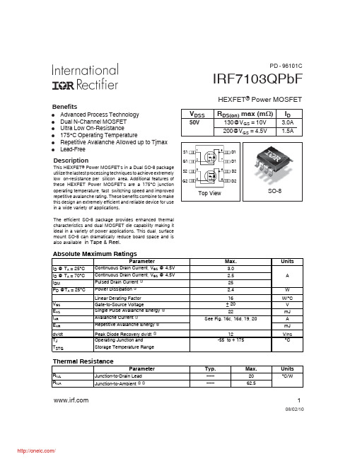
HEXFET ® Power MOSFETDescriptionThis HEXFET ® Power MOSFET's in a Dual SO-8 package utilize the lastest processing techniques to achieve extremely low on-resistance per silicon area. Additional features of these HEXFET Power MOSFET's are a 175°C junction operating temperature, fast switching speed and improved repetitive avalanche rating. These benefits combine to make this design an extremely efficient and reliable device for use in a wide variety of applications.The efficient SO-8 package provides enhanced thermal characteristics and dual MOSFET die capability making it ideal in a variety of power applications. This dual, surface mount SO-8 can dramatically reduce board space and is also available in Tape & Reel.08/02/10 1Benefitsl Advanced Process Technology l Dual N-Channel MOSFET l Ultra Low On-Resistancel 175°C Operating Temperaturel Repetitive Avalanche Allowed up to Tjmax lLead-FreeIRF7103QPbFV DSSR DS(on) max (m W)I D50V130@V GS = 10V 3.0A 200@V GS = 4.5V1.5APD - 96101CIRF7103QPbFSource-Drain Ratings and CharacteristicsNotes:Repetitive rating; pulse width limited bymax. junction temperature.Pulse width ≤ 400µs; duty cycle ≤ 2%.Surface mounted on 1 in square Cu boardStarting T J = 25°C, L = 4.9mHR G = 25Ω, I AS = 3.0A. (See Figure 12). I SD ≤ 2.0A, di/dt ≤ 155A/µs, V DD ≤ V (BR)DSS , T J ≤ 175°CLimited by T Jmax , see Fig.16c, 16d, 19, 20 for typical repetitive avalanche performance.ParameterMin.Typ.Max.Units Conditions V (BR)DSSDrain-to-Source Breakdown Voltage 50––––––V V GS = 0V, I D = 250µA∆V (BR)DSS /∆T JBreakdown Voltage Temp. Coefficient –––0.057–––V/°C Reference to 25°C, I D = 1mA ––––––130V GS = 10V, I D = 3.0A–––––– 200V GS = 4.5V, I D = 1.5A V GS(th)Gate Threshold Voltage 1.0––– 3.0V V DS = V GS , I D = 250µA g fs Forward Transconductance 3.4––––––S V DS = 15V, I D = 3.0A –––––– 2.0V DS = 40V, V GS = 0V––––––25V DS = 40V, V GS = 0V, T J = 55°C Gate-to-Source Forward Leakage ––––––100V GS = 20VGate-to-Source Reverse Leakage ––––––-100V GS = -20V Q g Total Gate Charge–––1015I D = 2.0A Q gs Gate-to-Source Charge––– 1.2–––nC V DS = 40V Q gd Gate-to-Drain ("Miller") Charge ––– 2.8–––V GS = 10V t d(on)Turn-On Delay Time ––– 5.1–––V DD = 25V t rRise Time––– 1.7–––I D = 1.0At d(off)Turn-Off Delay Time –––15–––R G = 6.0Ωt f Fall Time––– 2.3–––R D = 25ΩC iss Input Capacitance –––255–––V GS = 0V C oss Output Capacitance–––69–––pF V DS = 25V C rssReverse Transfer Capacitance–––29–––ƒ = 1.0MHzElectrical Characteristics @ T J = 25°C (unless otherwise specified)I GSS µAm ΩR DS(on)Static Drain-to-Source On-Resistance I DSS Drain-to-Source Leakage Current nAnsIRF7103QPbF 3Fig 3. Typical Transfer CharacteristicsFig 2. Typical Output CharacteristicsFig 1. Typical Output Characteristics Fig 4. Normalized On-ResistanceVs. Temperature3.06.09.012.015.0V GS , Gate-to-Source Voltage (V)1.0010.00100.00I D , D r a i n -t o -S o u r c e C u r r en t (Α)V DS , Drain-to-Source Voltage (V)I D , D r a i n -t o -S o u r c e C u r r e n t (A)V DS , Drain-to-Source Voltage (V)I D , D r a i n -t o -S o u r c e C u r r e n t (A )IRF7103QPbFGate-to-Source VoltageFig 5. Typical Capacitance Vs.Drain-to-Source Voltage Fig 8. Maximum Safe Operating AreaForward Voltage1101001000V DS , Drain-toSource Voltage (V)0.010.1110100I D , D r a i n -t o -S o u r c e C u r r e n t (A )110100V DS , Drain-to-Source Voltage (V)10100100010000C , C a p a c i t a n c e (p F )IRF7103QPbF 5Fig 11. Typical Effective Transient Thermal Impedance, Junction-to-AmbientCase TemperatureFig 10a. Switching Time Test CircuitV V d(on)rd(off)fFig 10b. Switching Time WaveformsV DDt 1 , Rectangular Pulse Duration (sec)IRF7103QPbF6Fig 13. Typical On-Resistance Vs. DrainCurrentFig 12. Typical On-Resistance Vs. GateVoltageFig 14. Typical Threshold Voltage Vs.Junction TemperatureFig 15. Typical Power Vs. Time-V GS, Gate -to -Source Voltage (V)R D S (o n ), D r a i n -t o -S o u r ce O n R e s i s t a n c e (Ω)T J , Temperature ( °C )V G S (t h ) G a t e t h r e s h o l d V o l t a g e (V )510152025303540I D , Drain Current (A)0.0000.5001.0001.5002.0002.500R D S (o n ) , D r a i n -t o -S o u r c e O n R e s i s t a n c e (Ω)Time (sec)P o w e r (W )IRF7103QPbF7VDSCurrent Sampling ResistorsV GSFig 17. Gate Charge Test Circuit Fig 18. Basic Gate Charge WaveformVs. Drain CurrentFig 16d. Unclamped Inductive WaveformsFig 16c. Unclamped Inductive Test CircuitI ASV DDIRF7103QPbFFig 19. Typical Avalanche Current Vs.PulsewidthFig 20. Maximum Avalanche EnergyVs. TemperatureNotes on Repetitive Avalanche Curves , Figures 15, 16:(For further info, see AN-1005 at )1. Avalanche failures assumption:Purely a thermal phenomenon and failure occurs at a temperature far in excess of T jmax . This is validated for every part type.2. Safe operation in Avalanche is allowed as long asT jmax is not exceeded.3. Equation below based on circuit and waveforms shown in Figures 12a, 12b.4. P D (ave) = Average power dissipation per single avalanche pulse.5. BV = Rated breakdown voltage (1.3 factor accounts for voltage increase during avalanche).6. I av = Allowable avalanche current.7. ∆T = Allowable rise in junction temperature, not to exceed T jmax (assumed as 25°C in Figure 15, 16). t av = Average time in avalanche. D = Duty cycle in avalanche = t av ·fZ thJC (D, t av ) = Transient thermal resistance, see figure 11)P D (ave) = 1/2 ( 1.3·BV·I av ) = D T/ Z thJCI av = 2D T/ [1.3·BV·Z th ]E AS (AR) = P D (ave)·t avtav (sec)A v a l a n c h e C u r r e n t (A)255075100125150175Starting T J , Junction Temperature (°C)0510152025E A R , A v a l a n c h e E n e r g y (m J )IRF7103QPbFSO-8 Package OutlineIRF7103QPbF10330.00(12.992) MAX.14.40 ( .566 )12.40 ( .488 )NOTES :1. CONTROLLING DIMENSION : MILLIMETER.2. OUTLINE CONFORMS TO EIA-481 & EIA-541.FEED DIRECTIONTERMINAL NUMBER 112.3 ( .484 )11.7 ( .461 )8.1 ( .318 )7.9 ( .312 )NOTES:1. CONTROLLING DIMENSION : MILLIMETER.2. ALL DIMENSIONS ARE SHOWN IN MILLIMETERS(INCHES).3. OUTLINE CONFORMS TO EIA-481 & EIA-541.SO-8 Tape and ReelIR WORLD HEADQUARTERS: 233 Kansas St., El Segundo, California 90245, USA Tel: (310) 252-7105TAC Fax: (310) 252-7903Visit us at for sales contact information .08/2010Data and specifications subject to change without notice.This product has been designed and qualified for the Industrial market.Qualification Standards can be found on IR’s Web site.分销商库存信息: IRIRF7103QTRPBF。
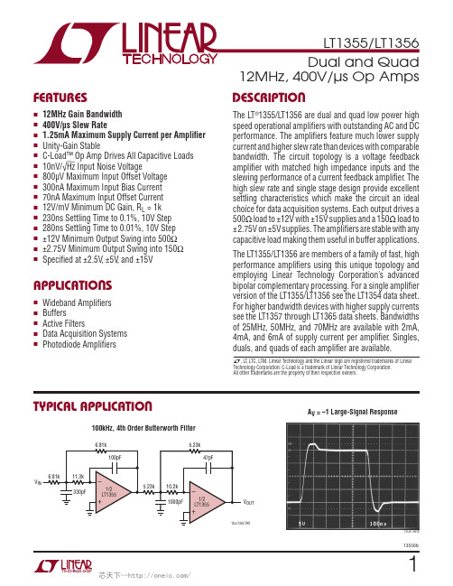
LT1355CN8#PB,LT1355CN8,LT1355CS8,LT1355CS8#TR,LT1355CS8#TRPBF,LT1356CN, 规格书,Datasheet 资料
For more information on lead free part marking, go to: /leadfree/ For more information on tape and reel specifications, go to: /tapeandreel/
芯天下--/
1
LT1355/LT1356 ABSOLUTE MAXIMUM RATINGS
(Note 1)
Total Supply Voltage (V+ to V –)..................................36V Differential Input Voltage (Transient Only) (Note 2).................................................................... ±10V Input Voltage.............................................................. ±VS Output Short-Circuit Duration (Note 3)............. Indefinite Operating Temperature Range (Note 7) LT1355C/LT1356C/LT1356I..................–40°C to 85°C LT1356H (TC)...................................... –40°C to 125°C
PIN CONFIGURATION
LT1355
OUT A –IN A +IN A
V–
TOP VIEW 1 2 3 4 A B
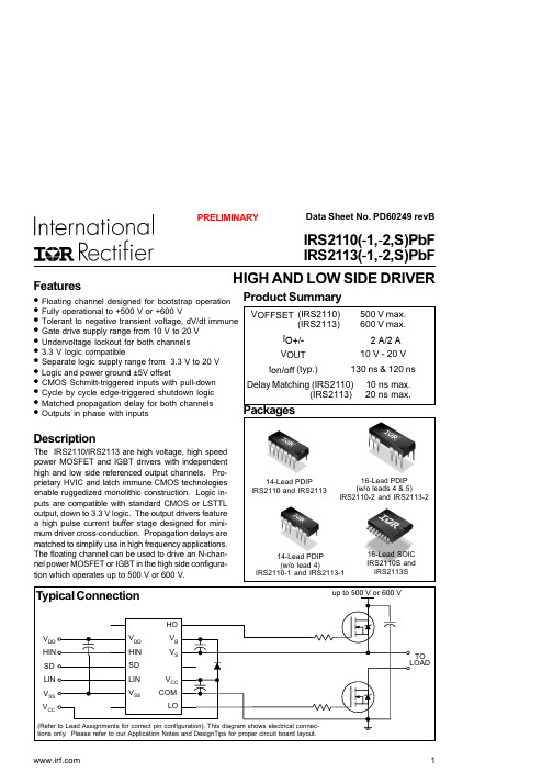
IRS2113STRPBF中文资料
150
°C
TL
Lead temperature (soldering, 10 seconds)
—
300
Note 1: All supplies are fully tested at 25 V, and an internal 20 V clamp exists for each supply.
Recommended Operating Conditions
(14 lead DIP) Package power dissipation @ TA ≤ +25 °C (16 lead SOIC)
VB - 20 VS - 0.3
-0.3 -0.3 -0.3 VCC - 20 VSS - 0.3 — — —
VB + 0.3 VB + 0.3 20 (Note 1) VCC + 0.3 VSS+20 (Note 1) VCC + 0.3 VDD + 0.3
Symbol
Definition
Min.
Max. Units
VB
High side floating supply voltage
(IRS2110) (IRS2113)
-0.3
520 (Note 1)
-0.3
620 (Note 1)
VS VHO VCC VLO VDD VSS VIN dVs/dt
PD
(IRS2110) (IRS2113)
Figure Min.
7
—
8
—
9
—
10
—
11
—
—
—
—
—
Typ. Max. Units Test Conditions
LTC1733EMSE#PBF;LTC1733EMSE;LTC1733EMSE#TR;LTC1733EMSE#TRPBF;中文规格书,Datasheet资料
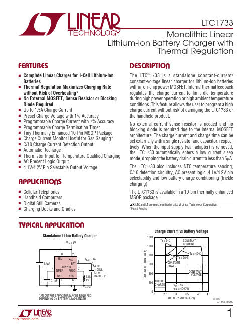
1 /2sn1733 1733fsInput Supply Voltage (V CC )........................................7V BAT............................................................................7V NTC, SEL, TIMER, PROG................–0.3V to V CC + 0.3V CHRG, FAULT, ACPR...................................–0.3V to 7V BAT Short-Circuit Duration...........................Continuous BAT Current (Note 2)..............................................1.6A PROG Current (Note 2)........................................1.6mA Junction Temperature...........................................125°C Operating Temperature Range (Note 3)...–40°C to 85°C Storage Temperature Range.................–65°C to 150°C Lead Temperature (Soldering, 10 sec)..................300°CABSOLUTE AXI U RATI GSW W WU PACKAGE/ORDER I FOR ATIOUUW (Note 1)ELECTRICAL CHARACTERISTICSSYMBOL PARAMETER CONDITIONSMIN TYP MAX UNITSV CC V CC Supply Voltage q 4.56.5V I CC V CC Supply CurrentCharger On; Current Mode; R PROG = 30k (Note 5)q 13mA Shutdown Mode; V PROG = 3V q 0.92mA V BAT V BAT Regulated Output Voltage SEL = 0V q 4.059 4.1 4.141V SEL = V CCq 4.158 4.2 4.242V I BATBattery Pin CurrentR PROG = 3k; Current Mode q465500535mA R PROG = 1k; Current Mode 1.3951.5 1.605A Shutdown Mode; V PROG = 3V±1±5µA Sleep Mode V CC < V BAT or V CC < (V UV – ∆V UV )±1±5µA I TRIKL Trickle Charge Current V BAT < 2V; R PROG = 3k q 355065mA V TRIKL Trickle Charge Trip Threshold V BAT Rising 2.48V ∆V TRIKL Trickle Charge Trip Hysteresis 100mVV UV V CC Undervoltage Lockout Voltage V CC Risingq4.2 4.5V ∆V UV V CC Undervoltage Lockout Hysteresis 150mV V MSD Manual Shutdown Threshold Voltage PROG Pin Voltage Rising2.15V V MSD-HYS Manual Shutdown Hysteresis Voltage100mV V ASDAutomatic Shutdown Threshold Voltage (V CC - V BAT ) Voltage Falling30mV (V CC - V BAT ) Voltage Rising60mVConsult LTC Marketing for parts specified with wider operating temperature ranges.ORDER PART NUMBER LTC1733EMSE T JMAX = 125°C, θJA = 40°C/W (Note 4)EXPOSED PAD IS GROUND.(MUST BE SOLDERED TO PCB FOR MAXIMUM HEAT TRANSFER).MSE PART MARKINGLTLX12345CHRG V CC FAULT TIMER GND109876ACPR BAT SEL PROG NTCTOP VIEWMSE EXPOSED PAD PACKAGE 10-LEAD PLASTIC MSOPThe q denotes the specifications which apply over the full operatingtemperature range, otherwise specifications are at T A = 25°C. V CC = 5V/3sn1733 1733fsNote 1: Absolute Maximum Ratings are those values beyond which the life of a device may be impaired.Note 2: The Absolute Maximum BAT Current Rating of 1.6A is guaranteed by design and current density calculations. The Absolute Maximum PROG Current Rating is guaranteed to be 1/1000 of BAT current rating by design.Note 3: The LTC1733E is guaranteed to meet performance specifications from 0°C to 70°C. Specifications over the –40°C to 85°C operatingSYMBOL PARAMETER CONDITIONSMINTYP MAXUNITSV PROG PROG Pin VoltageR PROG = 3k, I PROG = 500µA; Current Mode 1.5V I CHRG CHRG Pin Weak Pulldown Current V CHRG = 1V 25µA V CHRG CHRG Pin Output Low Voltage I CHRG = 5mA 0.35V V ACPR ACPR Pin Output Low Voltage I ACPR = 5mA 0.35V V FAULT FAULT Pin Output Low Voltage I FAULT = 5mA 0.35V I C/10End of Charge Indication Current Level R PROG = 3k 355065mA t TIMER TIMER AccuracyC TIMER = 0.1µF±10%V RECHRG Recharge Battery Voltage Threshold Battery Voltage Falling, SEL = 0V 3.9V Battery Voltage Falling, SEL = 5V 4.0V V NTC-HOT NTC Pin Hot Threshold Voltage V NTC Falling2.5V V HOT-HYS NTC Pin Hot Hysteresis Voltage 70mV V NTC-COLD NTC Pin Cold Threshold Voltage V NTC Rising4.375V V COLD-HYS NTC Pin Cold Hystersis Voltage 70mV V NTC-DIS NTC Pin Disable Threshold Voltage V NTC Rising 100mV V DIS-HYS NTC Pin Disable Hystersis Voltage 10mV V SEL-IL SEL Pin Threshold Input Low 0.3V V SEL-IH SEL Pin Threshold Input High 1V T LIM Junction Temperature in 105°C Constant-Temperature Mode R ONPower MOSFET “ON” Resistance375m Ωtemperature range are assured by design, characterization and correlation with statistical process controls.Note 4: Failure to solder the exposed backside of the package to the PC board will result in a thermal resistance much higher than 40°C/W.Note 5: Supply current includes PROG pin current but does not include any current delivered to the battery through the BAT pin.ELECTRICAL CHARACTERISTICST A = 25°C. V CC = 5V unless otherwise noted./4/5 /UUUPI FU CTIO SCHRG: Open-Drain Charge Status Output. When the battery is being charged, the CHRG pin is pulled low by an internal N-channel MOSFET. When the charge current drops to 10% of the full-scale current, the N-channel MOSFET latches off and a 25µA current source is con-nected from the CHRG pin to ground. The C/10 latch can be cleared by momentarily pulling the PROG pin above the 2.15V shutdown threshold, or by toggling V CC. When the timer runs out or the input supply is removed, the current source is disconnected and the CHRG pin is forced to a high impedance state.V CC: Positive Input Supply Voltage. When V CC is within 30mV of V BAT or less than the undervoltage lockout threshold, the LTC1733 enters sleep mode, dropping I BAT to less than 5µA. V CC can range from 4.5V to 6.5V. Bypass this pin with at least a 4.7µF ceramic capacitor to ground. FAULT: Open-Drain Fault Status Output. The FAULT open-drain logic signal indicates that the charger has timed out under trickle charge conditions (1/4 of total time period) or the NTC comparator is indicating an out-of-range battery temperature condition. When V BAT is less that 2.48V, trickle charging activates whereby the charge current drops to one tenth of its programmed value and the timer period is reduced by a factor of four. When one fourth of the timing period has elapsed, if V BAT is still less than 2.48V, trickle charging stops and the FAULT pin latches to ground. The fault can be cleared by toggling V CC, momen-tarily pulling the PROG pin above the 2.15V shutdown threshold, or pulling the BAT pin above 2.48V. If the NTC comparator is indicating an out-of-range battery tempera-ture condition, then the FAULT pin will pull to ground until the temperature returns to the acceptable range. TIMER: Timer Capacitor. The timer period is set by placing a capacitor, C TIMER, to ground. The timer period is: Time (Hours) = (C TIMER • 3 hr)/(0.1µF)Short the TIMER pin to ground to disable the internal timer function.GND: Ground. Connect exposed back package to ground. NTC: Input to the NTC (Negative Temperature Coefficient) Thermistor Temperature Monitoring Circuit. With an ex-ternal 10kΩ NTC thermistor to ground and a 1% resistor to V CC, this pin can sense the temperature of the battery pack and stop charging when it is out of range. When the voltage at this pin drops below (0.5)•(V CC) at hot tempera-tures or rises above (0.875)•(V CC) at cold, charging is suspended and the internal timer is frozen. The CHRG pin output status is not affected in this hold state. The FAULT pin is pulled to ground, but not latched. When the tempera-ture returns to an acceptable range, charging will resume and the FAULT pin is released. The NTC feature can be disabled by grounding the NTC pin.PROG: Charge Current Program, Shutdown Input and Charge Current Monitor Pin. The charge current is pro-grammed by connecting a resistor, R PROG to ground. When in constant-current mode, the LTC1733 servos the PROG pin voltage to 1.5V. In all modes the voltage on the PROG pin can be used to measure the charge current as follows:I CHG = (V PROG/R PROG) • 1000.The IC can be forced into shutdown by pulling the PROG pin above the 2.15V shutdown threshold voltage (note: it will not be pulled up when allowed to float).SEL: 4.1V/4.2V Battery Selection Input. Grounding this pin sets the battery float voltage to 4.1V, while connecting to V CC sets the voltage to 4.2V.BAT: Charge Current Output. A bypass capacitor of at least 1µF with a 1Ω series resistor is required to minimize ripple voltage when the battery is not present. A precision internal resistor divider sets the final float potential on this pin. The internal resistor divider is disconnected in sleep and shutdown modes.ACPR: Open-Drain Power Supply Status Output. When V CC is greater than the undervoltage lockout threshold and at least 30mV above V BAT, the ACPR pin will pull to ground. Otherwise, the pin is forced to a high impedance state./6sn1733 1733fs7 /The LTC1733 is a linear battery charger designed primarily for charging single cell lithium-ion batteries. Featuring an internal P-channel power MOSFET, the charger uses a constant-current/constant-voltage charge algorithm with programmable current and a programmable timer for charge termination. Charge current can be programmed up to 1.5A with a final float voltage accuracy of ±1%. No blocking diode or sense resistor is required thus dropping the external component count to three for the basic charger circuit. The CHRG, ACPR, and FAULT open-drain status outputs provide information regarding the status of the LTC1733 at all times. An NTC thermistor input provides the option of charge qualification using battery temperature.An internal thermal limit reduces the programmed charge current if the die temperature attempts to rise above a preset value of approximately 105°C. This feature protects the LTC1733 from excessive temperature, and allows the user to push the limits of the power handling capability of a given circuit board without risk of damaging the LTC1733 or the external components. Another benefit of the LTC1733 thermal limit is that charge current can be set according to typical, not worst-case, ambient temperatures for a given application with the assurance that the charger will auto-matically reduce the current in worst-case conditions. The charge cycle begins when the voltage at the V CC pin rises above the UVLO level and a program resistor is connected from the PROG pin to ground. At the beginning of the charge cycle, if the battery voltage is below 2.48V, the charger goes into trickle charge mode to bring the cell voltage up to a safe level for charging. The charger goes into the fast charge constant-current mode once the voltage on the BAT pin rises above 2.48V. In constant-current mode, the charge current is set by R PROG. When the battery approaches the final float voltage, the charge current begins to decrease as the LTC1733 switches to constant-voltage mode. When the current drops to 10% of the full-scale charge current, an internal comparator latches off the MOSFET at the CHRG pin and connects a weak current source to ground to indicate a near end-of-charge (C/10) condition. The C/10 latch can be cleared by momentarily pulling the PROG pin above the 2.15V shutdown threshold, or momentarily removing and reap-plying V CC.An external capacitor on the TIMER pin sets the total charge time. When this time elapses the charge cycle terminates and the CHRG pin assumes a high impedance state. To restart the charge cycle, simply remove the input voltage and reapply it, or force the PROG pin above the 2.15V shutdown threshold (note: simply floating the PROG pin will not restart the charging cycle.For lithium-ion and similar batteries that require accurate final float potential, the internal reference, voltage ampli-fier and the resistor divider provide regulation with ±1% (max) accuracy.When the input voltage is not present, the charger goes into a sleep mode, dropping battery drain current, I BAT, to less than 5µA. This greatly reduces the current drain on the battery and increases the standby time. The charger can be shut down (I CC = 0.9mA) by forcing the PROG pin above 2.15V.OPERATIOU/8sn1733 1733fs9sn1733 1733fsUndervoltage Lockout (UVLO)An internal undervoltage lockout circuit monitors the input voltage and keeps the charger in shutdown mode until V CC rises above the undervoltage lockout threshold. The UVLO circuit has a built-in hysteresis of 150mV. Furthermore, to protect against reverse current in the power MOSFET, the UVLO circuit keeps the charger in shutdown mode if V CC falls to within 30mV of the battery voltage. If the UVLO comparator is tripped, the charger will not come out of shutdown until V CC rises 60mV above the battery voltage.Trickle Charge and Defective Battery Detection At the beginning of a charge cycle, if the battery voltage is low (below 2.48V) the charger goes into trickle charge reducing the charge current to 10% of the full-scale current. If the low battery voltage persists for one quarter of the total charge time, the battery is assumed to be defective, the charge cycle is terminated, the CHRG pin output assumes a high impedance state, and the FAULT pin latches low. The fault can be cleared by toggling V CC ,temporarily forcing the PROG pin above 2.15V, or tempo-rarily forcing the BAT pin voltage above 2.48V.ShutdownThe LTC1733 can be shutdown (I CC = 0.9mA) by pulling the PROG pin above the 2.15V shutdown threshold volt-age. In shutdown the internal linear regulator is turned off,and the internal timer is reset.RechargeThe LTC1733 has the ability to recharge a battery assuming that the battery voltage has been charged above 4.05V (SEL = 5V) or 3.95V (SEL = 0V). Once above these thresholds, a new charge cycle will begin if the battery voltage drops below 4V (SEL = 5V) or 3.9V (SEL = 0V) due to either a load on the battery or self-discharge. The recharge circuit integrates the BAT pin voltage for a few milliseconds to prevent a transient from restarting the charge cycle.If the battery voltage remains below 2.48V during trickle charge for 1/4 of the programmed time, the battery may be defective and the charge cycle will end. In addition, therecharge comparator is disabled and a new charge cycle will not begin unless the input voltage is toggled, the PROG pin is pulled above the 2.15V shutdown threshold, or the BAT pin is pulled above the 2.48V trickle charge threshold.Programming Charge CurrentThe formula for the battery charge current (see Figure 1)is:I CHG = (I PROG ) • 1000= (1.5V / R PROG ) • 1000 or R PROG = 1500/I CHGwhere R PROG is the total resistance from the PROG pin to ground. Under trickle charge conditions, this current is reduced to 10% of the full-scale value.For example, if 500mA charge current is required,calculate:R PROG = 1500/0.5A = 3k ΩFor best stability over temperature and time, 1% metal-film resistors are recommended.If the charger is in constant-temperature or constant-voltage mode, the battery current can be monitored by measuring the PROG pin voltage as follows:I CHG = (V PROG / R PROG ) • 1000Programming the TimerThe programmable timer is used to terminate the charge cycle. The timer duration is programmed by an external capacitor at the TIMER pin. The total charge time is:Time (Hours) = (3 Hours) • (C TIMER / 0.1µF) or C TIMER = 0.1µF • Time (Hours)/3 (Hours)The timer starts when an input voltage greater than the undervoltage lockout threshold level is applied and the program resistor is connected to ground. After a time-out occurs, the charge current stops, and the CHRG output assumes a high impedance state to indicate that the charging has stopped. Connecting the TIMER pin to ground disables the timer function.APPLICATIO S I FOR ATIOW UUU /10 /分销商库存信息:LINEAR-TECHNOLOGYLTC1733EMSE#PBF LTC1733EMSE LTC1733EMSE#TR LTC1733EMSE#TRPBF。
IRF6648TRPBF;IRF6648TR1PBF;中文规格书,Datasheet资料
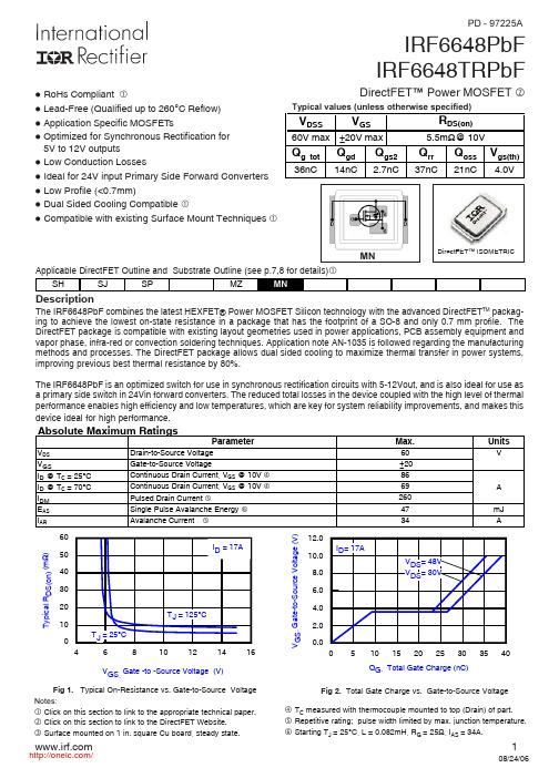
DirectFET Power MOSFETThe IRF6648PbF combines the latest HEXFET® Power MOSFET Silicon technology with the advanced DirectFET TM packag-ing to achieve the lowest on-state resistance in a package that has the footprint of a SO-8 and only 0.7 mm profile. The DirectFET package is compatible with existing layout geometries used in power applications, PCB assembly equipment and vapor phase, infra-red or convection soldering techniques. Application note AN-1035 is followed regarding the manufacturing methods and processes. The DirectFET package allows dual sided cooling to maximize thermal transfer in power systems,improving previous best thermal resistance by 80%.The IRF6648PbF is an optimized switch for use in synchronous rectification circuits with 5-12Vout, and is also ideal for use as a primary side switch in 24Vin forward converters. The reduced total losses in the device coupled with the high level of thermal performance enables high efficiency and low temperatures, which are key for system reliability improvements, and makes thisFig 1. Typical On-Resistance vs. Gate-to-Source VoltageFig 2. Total Gate Charge vs. Gate-to-Source VoltageDirectFET ISOMETRICMNl RoHs Compliantl Lead-Free (Qualified up to 260°C Reflow)l Application Specific MOSFET s lOptimized for Synchronous Rectification for 5V to 12V outputsl Low Conduction Lossesl Ideal for 24V input Primary Side Forward Converters l Low Profile (<0.7mm)l Dual Sided Cooling Compatiblel Compatible with existing Surface Mount TechniquesIRF6648PbF IRF6648TRPbFClick on this section to link to the appropriate technical paper. Click on this section to link to the DirectFET Website. T C measured with thermocouple mounted to top (Drain) of part. Repetitive rating; pulse width limited by max. junction temperature.Notes:46810121416V GS, Gate -to -Source Voltage (V)510152025303540Q G , Total Gate Charge (nC)PD - 97225AIRF6648PbFRepetitive rating; pulse width limited by max. junction temperature. Pulse width ≤ 400µs; duty cycle ≤ 2%.Notes:DD = 30V See Fig. 18GS = 0V iIRF6648PbFFig 3. Maximum Effective Transient Thermal Impedance, Junction-to-CaseUsed double sided cooling , mounting pad.Mounted on minimum footprint full size board with metalized back and with small clip heatsink.Notes:R θ is measured at T J of approximately 90°C.Surface mounted on 1 in. square Cu(still air).Mounted to a PCB with small clip heatsink (still air)Mounted on minimum footprint full size board with metalized back and with small clip heatsink (still air)t 1 , Rectangular Pulse Duration (sec)T h e r m a l R e s p o n s e ( Z )IRF6648PbFFig 7.Fig 8. Typical Capacitance vs.Drain-to-Source VoltageFig 9. Normalized Typical On-Resistance vs.Drain Current and Gate Voltage0.11101001000I D , D r a i n -t o -S o u r c e C u r r e n t (A )T J , Junction Temperature (°C)T y p i c a l R (N o r m a l i z e d )110100V DS , Drain-to-Source Voltage (V)100100010000C , C a p a c i t a n c e (p F )020*********I D , Drain Current (A)51015202530T y p i c a l R D S (o n ) (m Ω)IRF6648PbFFig 13. Threshold Voltage vs. TemperatureFig 12. Maximum Drain Current vs. Case TemperatureFig 10.Fig 14. Maximum Avalanche Energy vs. Drain Current01101001000I S D , R e v e r s e D r a i n C u r r e n t (A )255075100125150T C , Case Temperature (°C)0102030405060708090I D , D r a i n C u r r e n t (A )T J , Temperature ( °C )T y p i c a l V G S (t h ), G a t e t h r e s h o l d V o l t a g e (V )255075100125150Starting T J , Junction Temperature (°C)020406080100120140160180200E A S , S i n g l e P u l s e A v a l a n c h e E n e r g y (m J )IRF6648PbFDSCurrent Sampling ResistorsFig 15a. Gate Charge Test CircuitFig 15b. Gate Charge WaveformIdQgs1Qgs2Qgd QgodrFig 16b. Unclamped Inductive WaveformsI ASFig 16a. Unclamped Inductive Test CircuitFig 17b.Switching Time WaveformsV V DS90%10%d(on)d(off)rfFig 17a. Switching Time Test CircuitV DDIRF6648PbFFig 18. Diode Reverse Recovery Test Circuit for N-ChannelHEXFET®Power MOSFETs* V GS = 5V for Logic Level DevicesPlease see DirectFET application note AN-1035 for all details regarding the assembly of DirectFET.233 Kansas St., El Segundo, California 90245, USA Tel: (310) 252-7105TAC Fax: (310) 252-7903 Visit us at for sales contact information.08/06Note: For the most current drawings please refer to the IR website at:/package/分销商库存信息:IRIRF6648TRPBF IRF6648TR1PBF。
LTC4449EDCB#TRMPBF;LTC4449EDCB#TRPBF;LTC4449IDCB#TRMPBF;LTC4449IDCB#TRPBF;中文规格书,Datasheet资料
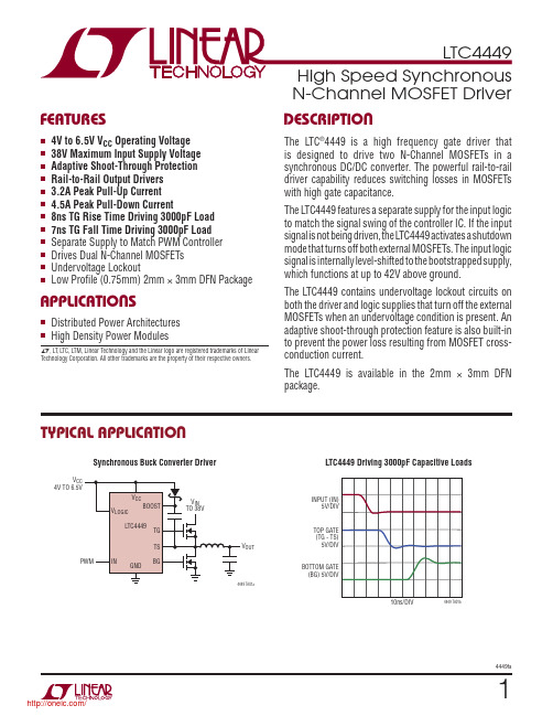
SYMBOL
PARAMETER
CONDITIONS
MIN TYP MAX UNITS
Input Signal (IN)
VIH(TG)
TG Turn-On Input Threshold
VIL(TG)
TG Turn-Off Input Threshold
VIH(BG)
BG Turn-On Input Threshold
FEATURES
n 4V to 6.5V VCC Operating Voltage n 38V Maximum Input Supply Voltage n Adaptive Shoot-Through Protection n Rail-to-Rail Output Drivers n 3.2A Peak Pull-Up Current n 4.5A Peak Pull-Down Current n 8ns TG Rise Time Driving 3000pF Load n 7ns TG Fall Time Driving 3000pF Load n Separate Supply to Match PWM Controller n Drives Dual N-Channel MOSFETs n Undervoltage Lockout n Low Profile (0.75mm) 2mm × 3mm DFN Package
IN = Floating
VCC Rising VCC Falling Hysteresis
4
6.5
V
300
400
μA
l 2.75 3.20 3.65
V
l 2.60 3.04 3.50
V
160
mV
- 1、下载文档前请自行甄别文档内容的完整性,平台不提供额外的编辑、内容补充、找答案等附加服务。
- 2、"仅部分预览"的文档,不可在线预览部分如存在完整性等问题,可反馈申请退款(可完整预览的文档不适用该条件!)。
- 3、如文档侵犯您的权益,请联系客服反馈,我们会尽快为您处理(人工客服工作时间:9:00-18:30)。
VGS = 20V
Qg
Total Gate Charge
7.2 11
ID = -1.6A
Qgs
Gate-to-Source Charge
Qgd
Gate-to-Drain ("Miller") Charge
1.4 2.1 2.3 3.4
nC VDS = -24V VGS = -10V, See Fig. 6 and 9
td(on)
Turn-On Delay Time
10
VDD = -15V
tr td(off) tf
Rise Time Turn-Off Delay Time Fall Time
12 ns ID = -1.6A
20
RG = 6.2Ω
8.4
Pulse width ≤ 300µs; duty cycle ≤ 2%.
ISD ≤ -1.6A, di/dt ≤ -140A/µs, VDD ≤ V(BR)DSS, Surface mounted on FR-4 board, t ≤ 5sec. TJ ≤ 150°C
2
/
-ID , Drain-to-Source Current (A)
100
Байду номын сангаас
VGS
TOP - 15V
- 10V
- 7.0V
- 5.5V
- 4.5V
- 4.0V
- 3.5V
BOTTOM - 3.0V
10
IRLMS5703PbF
100
VGS
TOP - 15V
- 10V
- 7.0V
VGS dv/dt TJ, TSTG
Parameter Continuous Drain Current, VGS @ -10V Continuous Drain Current, VGS @- 10V Pulsed Drain Current Power Dissipation Linear Derating Factor Gate-to-Source Voltage Peak Diode Recovery dv/dt Junction and Storage Temperature Range
IRLMS5703PbF
HEXFET® Power MOSFET
D
1
A
6
D
D
2
5
D
G
3
4
S
Top View
VDSS = -30V RDS(on) = 0.18Ω
Micro6™
Absolute Maximum Ratings
ID @ TA = 25°C ID @ TA = 70°C IDM PD @TA = 25°C
Diode Forward Voltage
trr
Reverse Recovery Time
Qrr
Reverse RecoveryCharge
Min.
Typ.
29 27
Max. Units
-1.7 A
-13
-1.2 V 44 ns 41 nC
Conditions
RD = 9.2Ω, See Fig. 10
Ciss
Input Capacitance
170
VGS = 0V
Coss
Output Capacitance
89 pF VDS = -25V
Crss
Reverse Transfer Capacitance
44
The Micro6™ package with its customized leadframe produces a HEXFET® power MOSFET with RDS(on) 60% less than a similar size SOT-23. This package is ideal for applications where printed circuit board space is at a premium. It's unique thermal design and RDS(on) reduction enables a current-handling increase of nearly 300% compared to the SOT-23.
2.0
ID = -1.6A
1.5
1.0
0.5
0.0 -60
VGS = -10V A
-40 -20 0 20 40 60 80 100 120 140 160
TJ , Junction Temperature (°C)
Fig 4. Normalized On-Resistance Vs. Temperature
= 1.0MHz, See Fig. 5
Source-Drain Ratings and Characteristics
Parameter
IS
Continuous Source Current
(Body Diode)
ISM
Pulsed Source Current
(Body Diode)
VSD
A
4.0
5.0
6.0
7.0
8.0
-VGS , Gate-to-Source Voltage (V)
Fig 3. Typical Transfer Characteristics
R DS(on) , Drain-to-Source On Resistance (Normalized)
3
-ID , Drain-to-Source Current (A)
/
IRLMS5703PbF
C, Capacitance (pF)
350
V GS = 0V,
f = 1MHz
Ciss = Cgs + Cgd , Cds SHORTED
300
Crss = Cgd
Coss = Cds + C gd
MOSFET symbol
D
showing the
integral reverse
G
p-n junction diode.
S
TJ = 25°C, IS = -1.6A, VGS = 0V
TJ = 25°C, IF = -1.6A
di/dt = -100A/µs
Notes:
Repetitive rating; pulse width limited by max. junction temperature. ( See fig. 11 )
Max. -2.4 -1.9 -13 1.7 13 ± 20 5.0 -55 to + 150
Units
A
W mW/°C
V V/ns
°C
Thermal Resistance Ratings
Parameter
RθJA
Maximum Junction-to-Ambient
Min.
-1.0 V VDS = VGS, ID = -250µA
gfs
Forward Transconductance
1.1 S VDS = -10V, ID = -0.80A
IDSS
Drain-to-Source Leakage Current
-1.0 -25
Typ.
Max 75
Units °C/W
1
1/18/05
/
IRLMS5703PbF
Electrical Characteristics @ TJ = 25°C (unless otherwise specified)
Parameter
Min. Typ. Max. Units
PD - 94896
l Generation V Technology l Micro6 Package Style l Ultra Low RDS(on) l P-channel MOSFET l Lead-Free
Description
Fifth Generation HEXFET® power MOSFETs from International Rectifier utilize advanced processing techniques to achieve extremely low on-resistance per silicon area. This benefit, combined with the fast switching speed and ruggedized device design that HEXFET® power MOSFETs are well known for, provides the designer with an extremely efficient and reliable device for use in a wide variety of applications.
4
-ID , Drain Current (A)
100
OPERATION IN THIS AREA LIMITED BY RDS(on)
10 100µs
1ms 1
10ms
TA = 25°C TJ = 150°C Single Pulse
0.1
Conditions
V(BR)DSS Drain-to-Source Breakdown Voltage
-30 V VGS = 0V, ID = -250µA
∆V(BR)DSS/∆TJ Breakdown Voltage Temp. Coefficient
