电源管理芯片AXP173 Datasheet
TEA1733PN1,112;中文规格书,Datasheet资料
3. Applications
All applications requiring efficient and cost-effective power supply solutions up to 75 W.
4. Ordering information
Table 1. Ordering information
C1 R1
C2 R2
R3
R4
Θ
Z1
TEA1733P
VINSENSE 5 PROTECT 6
4 ISENSE
R5
3 DRIVER
CTRL 7
OPTIMER 8
C3
2 GND 1 VCC
C4
R8
C5
S1 R10
R6
C6 R9
Fig 3. Typical configuration
R7
014aab131
7.2 Start-up and UnderVoltage LockOut (UVLO)
5 VINSENSE
014aab289
Fig 2. Pinning diagram SOT97-1 (DIP8)
6.2 Pin description
Table 2. Pin description
Symbol
Pin
VCC
1
GND
2
DRIVER
3
ISENSE
4
VINSENSE
5
PROTECT
6
CTRL
5. Block diagram
TEA1733P
GreenChip SMPS control IC
1 VCC
22 V
2 GND
M1A3P250-1FG144中文资料(microsemi)中文数据手册「EasyDatasheet - 矽搜」
以ProASIC3器件做出参考也适用于ARM功能ProASIC3器件.该ARM功能部件号开始与M1(Cortex-M1).
IV
v1.3
芯片中文手册,看全文,戳
1 - ProASIC3器件系列简介
概述
超出ProASIC功能
PLUS® 家庭.非易失性闪存技术使ProASIC3
设备是安全,低功耗,单芯片解决方案,上电即行(LAPU)优势.ProASIC3再编程,提供时间将
表 2•
ProASIC3 FPGA包装规格尺寸
包
QN48 CS121
长 ×宽 (毫米 \毫米)
6×6
6×6
标称面产品
(mm 2)
36
36
间距( mm)
0.4
0.5
高度( mm)
0.90
0.99
QN68 8×8
64
0.4 0.90
QN132 8×8
VQ100 14 × 14
28 × 28
低电量
•核心电压低功耗
•支持1.5 V-只有系统
•低阻抗闪光灯开关
高性能路由层次
•分段,分层路由和时钟结构
高级I / O
•700 MbpsDDR,LVDS,有能力I / O(A3P250及以上)
•1.5 V,1.8 V,2.5 V和3.3 V混合电压操作
表格 1 • ProASIC3产品系列
ProAS IC3器 件
ProASIC3器件支持ARM Cortex-M1处理器. ARM设备有开头M1A3P(Cortex-M1)和不支持 AES解密Actel订购数量.
闪存优点
降低购置成本
优点设计师超出低单位成本,性能和易用性.不比 基于SRAMFPGA,以Flash为基础ProASIC3器件允许所有功能是住在电;没有外部引导PROM是必需.上 电路板安全机制防止访问所有节目安排信息并启用FPGA逻辑安全远程更新.设计人员 可以进行安全远程在系统编程,以支持未来设计迭代和现场升级与信心,有价值知识产 权(IP)不能被复制或受到威胁.安全ISP可以使用行业标准AES算法来执行. ProASIC3系 列器件结构减轻需要在更高用户容量ASIC移植.这使得ProASIC3系列具有成本效益ASIC替代 解决方案,尤其是在消费类,网络/通信,计算,和航空电子市场应用程序.
axp173
DATASHEETV1.0 April 22 2010AXP173Enhanced Single Cell Li-Battery and Power System Management ICKrossPower© 2010 KrossPower Limited - All rights reservedAXP173Enhanced single Cell Li-Battery and Power System Management IC目录 1.概述(Summary)............................................................................................................................................... 30H 21H2.特性(Feature) .................................................................................................................................................. 41H 2H3.典型应用(Typical Application)....................................................................................................................... 52H 23H4.极限参数(Absolute Maximum Ratings) ....................................................................................................... 63H 24H5.电气特性(Electrical Characteristics) ............................................................................................................ 64H 25H6.典型特性(Typical Characteristics)................................................................................................................ 95H 26H7.管脚定义(Pin Description) ........................................................................................................................... 136H 27H8.功能框图(Functional Block Diagram) ........................................................................................................ 157H 28H9.控制和操作(Control and Operating)........................................................................................................... 168H 29H9.1 两种工作模式(Mode Description)...................................................................................................... 169H 30H9.2 开关机和复位(Power On/Off & Reset) ............................................................................................. 1610H 31H9.3 电源通路管理(IPS) .............................................................................................................................. 171H 32H9.4 自适应充电器(Adaptive Charger)...................................................................................................... 1912H 3H9.5 不同工作模式管脚功能区别(Mode Difference)................................................................................ 2213H 34H9.6 多路电源输出(Multi-Power Outputs)................................................................................................. 2314H 35H9.7 默认电压/启动时序的设置(Default Voltage/Timing Setting) .......................................................... 2415H 36H9.8 信号采集系统(Singal Capture) .......................................................................................................... 2516H 37H9.9 定时器(Timer) ...................................................................................................................................... 2517H 38H9.10 Host接口及中断(Host Interface and IRQ) ...................................................................................... 2618H 39H9.11 寄存器(Registers).............................................................................................................................. 2719H 40H10. 封装(Package) ............................................................................................................................................. 4320H 41HVQ.QW WPPIQPWE CCConfidentialPage 2/44AXP173Enhanced single Cell Li-Battery and Power System Management IC1.概述(Summary)AXP173 是高度集成的电源系统管理芯片,针对单芯锂电池(锂离子或锂聚合物)且需要多路电源转换 输出的应用,提供简单易用而又可以灵活配置的完整电源解决方案,充分满足目前日益复杂的应用处理 器系统对于电源相对复杂而精确控制的要求。
AXP152 Datasheet v1.0_cn
VQ.QW WPPIQPWE CC
Confidential
Page 4/34
3.典型应用(Typical Application)
10.封装(Package)............................................................................................... 34
VQ.QW WPPIQPWE CC
Confidential
Page 2/34
PGND2 6 DCDC2 7 DLDO1 8 DLDO2 9 DLDOIN 10
VQ.QW WPPIQPWE CC
Confidential
Page 3/34
2.特性(Feature)
AXP152
Enhanced Power Supply IC
• 4 路同步降压转换器 (DC-DC) o DC-DC1:PFM/PWM 两种工作模式,可在 1.7-3.5V 之间部分调节,驱动能力 1A o DC-DC2:PFM/PWM 两种工作模式,可在 0.7-2.275V 之间调节,25mV/step,驱动能 力 2A,支持 DVM o DC-DC3:PFM/PWM 两种工作模式,可在 0.7-3.5V 之间调节,50mV/step,驱动能力 1.2A o DC-DC4:PFM/PWM 两种工作模式,可在 0.7-3.5V 之间调节,25mV/step,驱动能力 1.2A
9.1 开关机和复位(Power On/Off & Reset) .......................................................................................... 15 9.2 多路电源输出(Multi-Power Outputs)............................................................................................. 17 9.3 默认电压/启动时序的设置(Default Voltage/Timing Setting) .................................................... 19 9.4 多功能管脚说明(Multi-Function Pin Description) ...................................................................... 19 9.5 定时器(Timer)...................................................................................................................................... 20 9.6 HOST 接口及中断(TWSI and IRQ) ................................................................................................... 20 9.7 寄存器(Registers) ................................................................................................................................ 22
AXP221+Datasheet+V1.2+20130326+
使用者应当承担全部责任去获取实现本文档方案可能需要的第三方授权,本公司对这些第三 方授权不承担任何明示或暗示的保证、费用补偿或其他责任。
1
概述
AXP221 是一款高度集成的电源系统管理芯片,针对单芯锂电池 ( 锂离子或锂聚合物 ) 且需要多路电 源转换输出的应用,提供简单易用而又可以灵活配置的完整电源解决方案,充分满足多核应用处理 器系统对于电源相对复杂而精确控制的要求。
AXP221 集成了一个效率高达 94% 的 USB3.0-Compatible Flash Charger,充电电流可达 2.2A;同时 支持 21 路电源输出(包含 5 路大电流 DCDC,最高效率可达 95%),包含电压 / 电流 / 温度监视等多 路 12-Bit ADC;为保证电源系统安全稳定,AXP221 还整合了过 / 欠压 (OVP/UVP)、过温 (OTP)、过流 (OCP) 等保护电路;独有的 E-Gauge ™电量计系统在保证高精度计量的同时大幅度减少了电池参数测试流程。
PAGE 3
Copyright © 2013 X-Powers Limited. All Rights Reserved.
仅供卓睿内部参考
Datasheet
Revision 1.2
AXP221
PMIC Optimized For Multi-Core High-Performance System
200mA
14 路线性稳压器 • LDOIO0/LDOIO1:低噪声 LDO, 0.7V~3.3V 可调节 ,100mV/step, 驱
SN54LS173AW中文资料
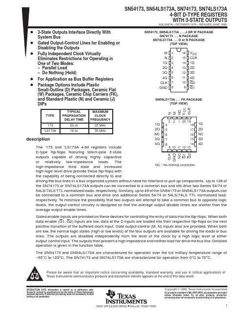
PACKAGING INFORMATIONOrderable Device Status(1)PackageType PackageDrawingPins PackageQtyEco Plan(2)Lead/Ball Finish MSL Peak Temp(3)JM38510/36101B2A ACTIVE LCCC FK201TBD Call TI Level-NC-NC-NC JM38510/36101BEA ACTIVE CDIP J161TBD Call TI Level-NC-NC-NC JM38510/36101BFA ACTIVE CFP W161TBD Call TI Level-NC-NC-NC JM38510/36101SEA ACTIVE CDIP J161TBD Call TI Level-NC-NC-NC JM38510/36101SFA ACTIVE CFP W161TBD Call TI Level-NC-NC-NC SN54173J ACTIVE CDIP J161TBD Call TI Level-NC-NC-NC SN54LS173AJ ACTIVE CDIP J161TBD Call TI Level-NC-NC-NCSN74173N OBSOLETE PDIP N16TBD Call TI Call TISN74LS173AD ACTIVE SOIC D1640Green(RoHS&no Sb/Br)CU NIPDAU Level-1-260C-UNLIMSN74LS173ADE4ACTIVE SOIC D1640Green(RoHS&no Sb/Br)CU NIPDAU Level-1-260C-UNLIMSN74LS173ADR ACTIVE SOIC D162500Green(RoHS&no Sb/Br)CU NIPDAU Level-1-260C-UNLIMSN74LS173ADRE4ACTIVE SOIC D162500Green(RoHS&no Sb/Br)CU NIPDAU Level-1-260C-UNLIMSN74LS173AN ACTIVE PDIP N1625Pb-Free(RoHS)CU NIPDAU Level-NC-NC-NCSN74LS173ANE4ACTIVE PDIP N1625Pb-Free(RoHS)CU NIPDAU Level-NC-NC-NCSN74LS173ANSR ACTIVE SO NS162000Green(RoHS&no Sb/Br)CU NIPDAU Level-1-260C-UNLIMSN74LS173ANSRE4ACTIVE SO NS162000Green(RoHS&no Sb/Br)CU NIPDAU Level-1-260C-UNLIM SNJ54173J ACTIVE CDIP J161TBD Call TI Level-NC-NC-NCSNJ54173W OBSOLETE CFP W16TBD Call TI Call TI SNJ54LS173AFK ACTIVE LCCC FK201TBD Call TI Level-NC-NC-NC SNJ54LS173AJ ACTIVE CDIP J161TBD Call TI Level-NC-NC-NC SNJ54LS173AW ACTIVE CFP W161TBD Call TI Level-NC-NC-NC (1)The marketing status values are defined as follows:ACTIVE:Product device recommended for new designs.LIFEBUY:TI has announced that the device will be discontinued,and a lifetime-buy period is in effect.NRND:Not recommended for new designs.Device is in production to support existing customers,but TI does not recommend using this part in a new design.PREVIEW:Device has been announced but is not in production.Samples may or may not be available.OBSOLETE:TI has discontinued the production of the device.(2)Eco Plan-The planned eco-friendly classification:Pb-Free(RoHS)or Green(RoHS&no Sb/Br)-please check /productcontent for the latest availability information and additional product content details.TBD:The Pb-Free/Green conversion plan has not been defined.Pb-Free(RoHS):TI's terms"Lead-Free"or"Pb-Free"mean semiconductor products that are compatible with the current RoHS requirements for all6substances,including the requirement that lead not exceed0.1%by weight in homogeneous materials.Where designed to be soldered at high temperatures,TI Pb-Free products are suitable for use in specified lead-free processes.Green(RoHS&no Sb/Br):TI defines"Green"to mean Pb-Free(RoHS compatible),and free of Bromine(Br)and Antimony(Sb)based flame retardants(Br or Sb do not exceed0.1%by weight in homogeneous material)(3)MSL,Peak Temp.--The Moisture Sensitivity Level rating according to the JEDEC industry standard classifications,and peak solder temperature.Important Information and Disclaimer:The information provided on this page represents TI's knowledge and belief as of the date that it is provided.TI bases its knowledge and belief on information provided by third parties,and makes no representation or warranty as to the accuracy of such information.Efforts are underway to better integrate information from third parties.TI has taken and continues to take reasonable steps to provide representative and accurate information but may not have conducted destructive testing or chemical analysis on incoming materials and chemicals.TI and TI suppliers consider certain information to be proprietary,and thus CAS numbers and other limited information may not be available for release.In no event shall TI's liability arising out of such information exceed the total purchase price of the TI part(s)at issue in this document sold by TI to Customer on an annual basis.IMPORTANT NOTICETexas Instruments Incorporated and its subsidiaries (TI) reserve the right to make corrections, modifications, enhancements, improvements, and other changes to its products and services at any time and to discontinue any product or service without notice. Customers should obtain the latest relevant information before placing orders and should verify that such information is current and complete. All products are sold subject to TI’s terms and conditions of sale supplied at the time of order acknowledgment.TI warrants performance of its hardware products to the specifications applicable at the time of sale in accordance with TI’s standard warranty. T esting and other quality control techniques are used to the extent TI deems necessary to support this warranty. Except where mandated by government requirements, testing of all parameters of each product is not necessarily performed.TI assumes no liability for applications assistance or customer product design. Customers are responsible for their products and applications using TI components. T o minimize the risks associated with customer products and applications, customers should provide adequate design and operating safeguards.TI does not warrant or represent that any license, either express or implied, is granted under any TI patent right, copyright, mask work right, or other TI intellectual property right relating to any combination, machine, or process in which TI products or services are used. Information published by TI regarding third-party products or services does not constitute a license from TI to use such products or services or a warranty or endorsement thereof. Use of such information may require a license from a third party under the patents or other intellectual property of the third party, or a license from TI under the patents or other intellectual property of TI.Reproduction of information in TI data books or data sheets is permissible only if reproduction is without alteration and is accompanied by all associated warranties, conditions, limitations, and notices. Reproduction of this information with alteration is an unfair and deceptive business practice. TI is not responsible or liable for such altered documentation.Resale of TI products or services with statements different from or beyond the parameters stated by TI for that product or service voids all express and any implied warranties for the associated TI product or service and is an unfair and deceptive business practice. TI is not responsible or liable for any such statements. Following are URLs where you can obtain information on other Texas Instruments products and application solutions:Products ApplicationsAmplifiers Audio /audioData Converters Automotive /automotiveDSP Broadband /broadbandInterface Digital Control /digitalcontrolLogic Military /militaryPower Mgmt Optical Networking /opticalnetwork Microcontrollers Security /securityTelephony /telephonyVideo & Imaging /videoWireless /wirelessMailing Address:Texas InstrumentsPost Office Box 655303 Dallas, Texas 75265Copyright 2005, Texas Instruments Incorporated。
PCI-1733 快速说明书
PCI-1733 快速安装使用手册
图 2-6 安装完后 labview 驱动帮助手册快捷方式为:开始/ 程序/ Advantech Automation/LabView/XXXX.chm 。 默 认 安 装 下 也 可 以 在 C:\Program Files\National Instruments\LabVIEW 7.0\help\Advantech 中直接打开 labview 驱动帮助手册。
Active Daq 控 件 使 用 手 册 快 捷 方 式 为 开 始 / 程 序 / Advantech Automation/ActiveDaq Pro/ ActiveDAQPro.chm 。 默 认 安 装 下 也 可 以 在 C:\Program Files\ADVANTECH\ActiveDAQ Pro 中直接打开 Active Daq 驱动手 册:ActiveDAQPro.chm。
PCI-1733 具有宽的输入范围,适合于很多供电电源 12VDC 和 24VDC 的工 业应用场合。
1.1.3 PCI 总线即插即用
PCI-1733 是一款 PCI 总线卡,完全符合 PCI 总线的 Rev2.1 标准。所有与 总线相关的配置,比如基地址和中断分配等都是由软件自动完成的。用户无须进 行跳线或 DIP 拨码开关的配置。
1.2 特点: .........................................................................................2 第二章 安装与测试 ............................................. 2
1
PCI-1733 快速安装使用手册
2500VDC 的电压,保护您的系统免受意外损坏。如果连接到具有浪涌保护的外 部输入源,PCI-1733 可以提供最大 2000VDC 的 ESD(静电释放)保护。即使 输入电压上升到 70VDC,PCI-1733 仍然可以正常工作一段时间。
AXP199 Datasheet v1.01_cn
应用产品
z 手持式移动设备 智能移动电话, PMP/MP4, 数 码相机, 数字摄像机, 手持导 航设备 GPS, PDA, 手持数字 广播电视接收机
z 移动互联网设备 MID z 数码相框,便携 DVD 播放器,
超便携移动电脑 UMPC and UMPC-like,学习机 z 应用处理器电路系统
• 电源管理 (IPS) o 宽输入电压范围: 2.9V~6.3V (AMR:-0.3V~15V) o 可配置的高效智慧电能平衡“IPS™”系统 o 自适应 USB 或交流适配器限压限流
(4.4V/500mA/100mA) o 内部理想二极管的等效内阻小于 100mΩ • 全集成充电器 (Charger) o 内置 MOSFET 最大充电电流可达 1.4A o 支持电池温度监测 o 全面支持 USB 充电,符合规范要求 o 充电精度高,误差小于 0.5% o 支持 4.1V/4.15V/4.2V/4.36V 等多种电池 o 自动进行充电流程控制 o 可直接驱动 LED 指示充电状态 o 根据系统负载情况自动调节充电电流 • 备用电池 (Backup Battery) o 可使用备用电池给 RTC 模块供电 o 支持备用电池充电,可设置充电电流 • 3 路同步降压转换器 (DC-DC) o DC-DC1:可在 0.7V~3.5V 之间调节,
AXP199 内部集成了一个自适应的 USB-Compatible 的充电器,3 路降压转换器(Buck DC-DC converter),4 路线性稳压器(LDO),电压/电流/温度监视等多路 12-Bit ADC。为保证电源系统安全稳定, AXP199 还整合了过/欠压(OVP/UVP)、过温(OTP)、过流(OCP)等保护电路。
南京拓品微电子有限公司 TP4100 TP4101 TP4102 线性锂电池 充电、放电保护芯片 数
南京拓品微电子有限公司NanJing Top Power ASIC Corp.数据手册DATASHEETTP4100/TP4101/TP4102 (1000mA/500mA/1000mA线性锂电池充电、放电保护芯片)特点·首创5V电源反接保护;·兼容大小3mA-1000mA的可编程充电电流;·锂电池正负极反接保护;·涓流-恒定电流-恒定电压三段式充电;·充电模式电源功率自适应;·精度达到±1%的4.2V预设充电电压;·最高输入可达8V;·20%恒流预充电;·C/10充电终止;·充电待机模式下的电源电流80uA,·放电模式下BAT待机电流4uA;·电池2.6V欠压保护停机,充电自恢复;·过充保护,输出短路保护,输出过流保护;·保护后,8秒后自恢复;·多种封装DFN3*3-8/TSOT23-6/DFN2*2-8。
应用·微型锂电池设备·可穿戴、高集成度锂电池设备·锂电池便携设备等典型应用TP4100单节锂离子电池1A充电电路绝对最大额定值·输入电源电压(VCC):-5.5V~9V ·PROG:-0.3V~VCC+0.3V·BAT:-4.2V~9V·CHRG:-0.3V~9V·BAT短路持续时间:连续·BAT引脚电流:1200mA·PROG引脚电流:1500uA·最大结温:145℃·工作环境温度范围:-40℃~85℃·贮存温度范围:-65℃~125℃·引脚温度(焊接时间10秒):260℃1A电流完整的充电循环(1000mAh)描述TP4100/TP4101/TP4102是一款完整的单节锂离子电池充电管理、放电保护芯片,首创5V电源正负极反接保护,带电池正负极反接保护,兼容大小3mA-1000mA充电电流。
IRMCK311TR;中文规格书,Datasheet资料
Data Sheet No. PD60338IRMCK311 Dual Channel Sensorless Motor Control IC forAppliancesFeaturesMCE TM (Motion Control Engine) - Hardware based computation engine for high efficiency sinusoidal sensorless control of permanent magnet AC motor Integrated Power Factor Correction controlSupports both interior and surface permanent magnet motorsBuilt-in hardware peripheral for single shunt current feedback reconstructionNo external current or voltage sensing operational amplifier requiredDual channel three/two-phase Space Vector PWM Three-channel analog output (PWM)Embedded 8-bit high speed microcontroller (8051) for flexible I/O and man-machine controlJTAG programming port for emulation/debugger Two serial communication interface (UART)I2C/SPI serial interfaceWatchdog timer with independent analog clockThree general purpose timers/countersTwo special timers: periodic timer, capture timer Internal ‘One-Time Programmable’ (OTP) memory and internal RAM for final production usagePin compatible with IRMCF311 RAM version1.8V/3.3V CMOS Product SummaryMaximum crystal frequency 60 MHz Maximum internal clock (SYSCLK) frequency 128 MHz Maximum 8051 clock frequency 33 MHz Sensorless control computation time 11 μsec typ MCE TM computation data range 16 bit signed 8051 OTP Program memory 56K bytes MCE program and Data RAM 8K bytes GateKill latency (digital filtered) 2 μsec PWM carrier frequency counter 16 bits/ SYSCLK A/D input channels 6 A/D converter resolution 12 bits A/D converter conversion speed 2 μsec 8051 instruction execution speed 2 SYSCLK Analog output (PWM) resolution 8 bits UART baud rate (typ) 57.6K bps Number of I/O (max) 14 Package (lead-free) QFP64 Operating temperature -40°C ~ 85°CDescriptionIRMCK311 is a high performance OTP based motion control IC designed primarily for appliance applications. IRMCK311 is designed to achieve low cost and high performance control solutions for advanced inverterized appliance motor control. IRMCK311 contains two computation engines. One is Motion Control Engine (MCE TM) for sensorless control of permanent magnet motors; the other is an 8-bit high-speed microcontroller (8051). Both computation engines are integrated into one monolithic chip. The MCE TM contains a collection of control elements such as Proportional plus Integral, Vector rotator, Angle estimator, Multiply/Divide, Low loss SVPWM, Single Shunt IFB. The user can program a motion control algorithm by connecting these control elements using a graphic compiler. Key components of the sensorless control algorithms, such as the Angle Estimator, are provided as complete pre-defined control blocks implemented in hardware. A unique analog/digital circuit and algorithm to fully support single shunt current reconstruction is also provided. The 8051 microcontroller performs 2-cycle instruction execution (16MIPS at 33MHz). The MCE and 8051 microcontroller are connected via dual port RAM to process signal monitoring and command input. An advanced graphic compiler for the MCE TM is seamlessly integrated into the MATLAB/Simulink environment, while third party JTAG based emulator tools are supported for 8051 developments. IRMCK311 comes with a small QFP64 pin lead-free package.TABLE OF CONTENTS1 Overview (5)2 IRMCK311 Block Diagram and Main Functions (6)3 Pinout (8)4 Input/Output of IRMCK311 (9)4.1 8051 Peripheral Interface Group (10)4.2 Motion Peripheral Interface Group (10)4.3 Analog Interface Group (11)4.4 Power Interface Group (11)4.5 Test Interface (12)5 Application Connections (13)6 DC Characteristics (14)6.1 Absolute Maximum Ratings (14)6.2 System Clock Frequency and Power Consumption (14)6.3 Digital I/O DC Characteristics (15)6.4 PLL and Oscillator DC Characteristics (15)6.5 Analog I/O DC Characteristics (16)6.6 Under Voltage Lockout DC Characteristics (17)6.7 AREF Characteristics (17)7 AC Characteristics (18)7.1 PLL AC Characteristics (18)7.2 Analog to Digital Converter AC Characteristics (19)7.3 Op Amp AC Characteristics (19)7.4 SYNC to SVPWM and A/D Conversion AC Timing (20)7.5 GATEKILL to SVPWM AC Timing (21)7.6 Interrupt AC Timing (21)7.7 I2C AC Timing (22)7.8 SPI AC Timing (23)7.8.1 SPI Write AC timing (23)7.8.2 SPI Read AC Timing (24)7.9 UART AC Timing (25)7.10 CAPTURE Input AC Timing (26)7.11 JTAG AC Timing (27)7.12 OTP Programming Timing (28)8 I/O Structure (29)9 Pin List (32)Dimensions (35)10 Package11 Part Marking Information (36)Information (36)12 OrderingTABLE OF FIGURESFigure 1. Typical Application Block Diagram Using IRMCK311 (5)Figure 2. IRMCK311 Internal Block Diagram (6)Figure 3. IRMCK311 Pin Configuration (8)Figure 4. Input/Output of IRMCK311 (9)Figure 5. Application Connection of IRMCK311 (13)Figure 6. Clock Frequency vs. Power Consumption (14)Figure 7 Crystal oscillator circuit (18)Figure 8 Voltage droop of sample and hold (19)Figure 9 SYNC to SVPWM and A/D conversion AC Timing (20)Figure 10 GATEKILL to SVPWM AC Timing (21)Figure 11 Interrupt AC Timing (21)Figure 12 I2C AC Timing (22)Figure 13 SPI AC Timing (23)Figure 14 SPI Read AC Timing (24)Figure 15 UART AC Timing (25)Figure 16 CAPTURE Input AC Timing (26)Figure 17 JTAG AC Timing (27)Figure 18 OTP Programming Timing (28)Figure 19 All digital I/O except motor PWM output (29)Figure 20 RESET, GATEKILL I/O (29)Figure 21 Analog input (30)Figure 22 Analog operational amplifier output and AREF I/O structure (30)Figure 23 VPP programming pin I/O structure (30)Figure 24 VSS and AVSS pin structure (31)Figure 25 VDD1 and VDDCAP pin structure (31)Figure 26 XTAL0/XTAL1 pins structure (31)TABLE OF TABLESTable 1. Absolute Maximum Ratings (14)Table 2. System Clock Frequency (14)Table 3. Digital I/O DC Characteristics (15)Table 4. PLL DC Characteristics (15)Table 5. Analog I/O DC Characteristics (16)Table 6. UVcc DC Characteristics (17)Table 7. AREF DC Characteristics (17)Table 8. PLL AC Characteristics (18)Table 9. A/D Converter AC Characteristics (19)Table 10. Current Sensing OP Amp AC Characteristics (19)Table 11. SYNC AC Characteristics (20)Table 12. GATEKILL to SVPWM AC Timing (21)Table 13. Interrupt AC Timing (21)Table 14. I2C AC Timing (22)Table 15. SPI Write AC Timing (23)Table 16. SPI Read AC Timing (24)Table 17. UART AC Timing (25)Table 18. CAPTURE AC Timing (26)Table 19. JTAG AC Timing (27)Table 20. OTP Programming Timing (28)Table 21. Pin List (32)1 OverviewIRMCK311 is a new International Rectifier integrated circuit device primarily designed as a one-chip solution for complete inverter controlled appliance dual motor control applications. Unlike a traditional microcontroller or DSP, the IRMCK311 provides a built-in closed loop sensorless control algorithm using the unique Motion Control Engine (MCE TM) for permanent magnet motors. The MCE TM consists of a collection of control elements, motion peripherals, a dedicated motion control sequencer and dual port RAM to map internal signal nodes. IRMCK311 also employs a unique single shunt current reconstruction circuit to eliminate additional analog/digital circuitry and enables a direct shunt resistor interface to the IC. The sensorless control is the same for both motors with a single shunt current sensing capability. Motion control programming is achieved using a dedicated graphical compiler integrated into the MATLAB/Simulink TM development environment. Sequencing, user interface, host communication, and upper layer control tasks can be implemented in the 8051 high-speed 8-bit microcontroller. The 8051 microcontroller is equipped with a JTAG port to facilitate emulation and debugging tools. Figure 1 shows a typical application schematic using IRMCK311.IRMCK311 is intended for volume production purpose and contains 64K bytes of OTP (One Time Programming) ROM, which can be programmed through a JTAG port. For a development purpose use, IRMCF311 contains a 48k byte of RAM in place of program OTP to facilitate an application development work. Both IRMCF311 and IRMCK311 come in the same 64-pin QFP package with identical pin configuration to facilitate PC board layout and transition to mass productionFigure 1. Typical Application Block Diagram Using IRMCK3112 IRMCK311 Block Diagram and Main FunctionsM o t i o n C o n t r o l B u sFigure 2. IRMCK311 Internal Block DiagramIRMCK311 contains the following functions for sensorless AC motor control applications:• Motion Control Engine (MCE TM )o Proportional plus Integral block o Low pass filtero Differentiator and lag (high pass filter) o Ramp o Limito Angle estimate (sensorless control) o Inverse Clark transformation o Vector rotator o Bit latch o Peak detect o Transitiono Multiply-divide (signed and unsigned)o Divide (signed and unsigned)o Addero Subtractoro Comparatoro Countero Accumulatoro Switcho Shifto ATAN (arc tangent)o Function block (any curve fitting, nonlinear function)o16-bit wide Logic operations (AND, OR, XOR, NOT, NEGATE)o MCE TM program and data memory (6K byte). Note 1o MCE TM control sequencer• 8051 microcontrollero Three 16-bit timer/counterso16-bit periodic timero16-bit analog watchdog timero16-bit capture timero Up to 36 discrete I/Oso Eleven-channel 12-bit A/DFive buffered channels (0 – 1.2V input)One unbuffered channel (0 – 1.2V input)o JTAG port (4 pins)o Up to three channels of analog output (8-bit PWM)o Two UARTo I2C/SPI porto 64K byte Note 1program One-Time Programmable memoryo2K byte data RAM. Note 2Note 1: Total size of OTP memory is 64K byte, however MCE program occupiesmaximum 8K byte which will be loaded into internal RAM at a powerup/bootprocess. Therefore only 56K byte OTP memory area is usable for 8051microcontroller.Note 2: Total size of RAM is 8K byte including MCE program, MCE data, and 8051data. Different sizes can be allocated depending on applications.3 PinoutXTAL0XTAL1P1.1/RXD P1.2/TXDVDD1VSS VDD2P1.3/SYNC/SCKP1.4/CAPP 3.6/R X D 1P 3.7/T X D 1FPWMVL FPWMUL V S SV D D 2A V D DA V S SA I N 0A R E FP 2.7/A O P W M 1P 2.6/A O P W M 0CPWMUH CPWMVH CPWMWH CPWMUL CPWMVL CPWMWL CGATEKILL VDD1VSS I F B C OI F B C +I F B C -P L L V S SP L L V D DR E S E TN CT C KP 5.3/T D IP 5.2/T D OP 5.1/T M SS D A /C S 0S C L /S O -S I /V P PP 5.0/P F C G K I L LP F C P W M V S SFGATEKILL FPWMWL VAC-VAC+VACO IPFCO IPFC+IPFC-I F B F OI F B F +I F B F -P3.0/INT2/CS1C M E X TFPWMVH FPWMUHFPWMWH A I N 1P 3.2/I N T 0Figure 3. IRMCK311 Pin Configuration4 Input/Output of IRMCK311All I/O signals of IRMCK311 are shown in Figure 4. All I/O pins are 3.3V logic interface except A/D interface pins.Figure 4. Input/Output of IRMCK3114.1 8051 Peripheral Interface GroupUART InterfaceP1.1/RXD Input, Receive data to IRMCK311, can be configured as P1.1P1.2/TXD Output, Transmit data from IRMCK311, can be configured as P1.22nd channel Receive data to IRMCK311, can be configured as P3.6 P3.6/RXD1 Input,P3.7/TXD1 Output,2nd channel Transmit data from IRMCK311, can be configured as P3.7Discrete I/O InterfaceP1.3/SYNC/SCK Input/output port 1.3, can be configured as SYNC output or SPI clock P1.4/CAP Input/output port 1.4, can be configured as Capture Timer inputP3.0/INT2/CS1 Input/output port 3.0, can be configured as external interrupt 2 or SPIchip select 1P3.2/INT0 Input/output port 3.2, can be configured as external interrupt 0Analog Output InterfaceP2.6/AOPWM0 Input/output, can be configured as 8-bit PWM output 0 withprogrammable carrier frequencyP2.7/AOPWM1 Input/output, can be configured as 8-bit PWM output 1 withprogrammable carrier frequencyCrystal InterfaceXTAL0 Input, connected to crystalXTAL1 Output, connected to crystalReset InterfaceRESET Inout, system reset, needs to be pulled up to VDD1 but doesn’t requireexternal RC time constantI2C/SPI InterfaceSCL/SO-SI/VPP Output, I2C clock output, SPI SO-SII2C Data line, Chip Select 0 of SPISDA/CS0 Input/output,P3.0/INT2/CS1 Input/output port 3.0, can be configured as external interrupt 2 or SPIchip select 1P1.3/SYNC/SCK Input/output port 1.3, can be configured as SYNC output or SPI clock 4.2 Motion Peripheral Interface GroupPWMCPWMUH Output, motor 1 PWM phase U high side gate signalCPWMUL Output, motor 1 PWM phase U low side gate signalCPWMVH Output, motor 1 PWM phase V high side gate signalCPWMVL Output, motor 1 PWM phase V low side gate signalCPWMWH Output, motor 1 PWM phase W high side gate signalCPWMWL Output, motor 1 PWM phase W low side gate signalFPWMUH Output, motor 2 PWM phase U high side gate signalFPWMUL Output, motor 2 PWM phase U low side gate signal分销商库存信息: IRIRMCK311TR。
LTC1733EMSE#PBF;LTC1733EMSE;LTC1733EMSE#TR;LTC1733EMSE#TRPBF;中文规格书,Datasheet资料
1 /2sn1733 1733fsInput Supply Voltage (V CC )........................................7V BAT............................................................................7V NTC, SEL, TIMER, PROG................–0.3V to V CC + 0.3V CHRG, FAULT, ACPR...................................–0.3V to 7V BAT Short-Circuit Duration...........................Continuous BAT Current (Note 2)..............................................1.6A PROG Current (Note 2)........................................1.6mA Junction Temperature...........................................125°C Operating Temperature Range (Note 3)...–40°C to 85°C Storage Temperature Range.................–65°C to 150°C Lead Temperature (Soldering, 10 sec)..................300°CABSOLUTE AXI U RATI GSW W WU PACKAGE/ORDER I FOR ATIOUUW (Note 1)ELECTRICAL CHARACTERISTICSSYMBOL PARAMETER CONDITIONSMIN TYP MAX UNITSV CC V CC Supply Voltage q 4.56.5V I CC V CC Supply CurrentCharger On; Current Mode; R PROG = 30k (Note 5)q 13mA Shutdown Mode; V PROG = 3V q 0.92mA V BAT V BAT Regulated Output Voltage SEL = 0V q 4.059 4.1 4.141V SEL = V CCq 4.158 4.2 4.242V I BATBattery Pin CurrentR PROG = 3k; Current Mode q465500535mA R PROG = 1k; Current Mode 1.3951.5 1.605A Shutdown Mode; V PROG = 3V±1±5µA Sleep Mode V CC < V BAT or V CC < (V UV – ∆V UV )±1±5µA I TRIKL Trickle Charge Current V BAT < 2V; R PROG = 3k q 355065mA V TRIKL Trickle Charge Trip Threshold V BAT Rising 2.48V ∆V TRIKL Trickle Charge Trip Hysteresis 100mVV UV V CC Undervoltage Lockout Voltage V CC Risingq4.2 4.5V ∆V UV V CC Undervoltage Lockout Hysteresis 150mV V MSD Manual Shutdown Threshold Voltage PROG Pin Voltage Rising2.15V V MSD-HYS Manual Shutdown Hysteresis Voltage100mV V ASDAutomatic Shutdown Threshold Voltage (V CC - V BAT ) Voltage Falling30mV (V CC - V BAT ) Voltage Rising60mVConsult LTC Marketing for parts specified with wider operating temperature ranges.ORDER PART NUMBER LTC1733EMSE T JMAX = 125°C, θJA = 40°C/W (Note 4)EXPOSED PAD IS GROUND.(MUST BE SOLDERED TO PCB FOR MAXIMUM HEAT TRANSFER).MSE PART MARKINGLTLX12345CHRG V CC FAULT TIMER GND109876ACPR BAT SEL PROG NTCTOP VIEWMSE EXPOSED PAD PACKAGE 10-LEAD PLASTIC MSOPThe q denotes the specifications which apply over the full operatingtemperature range, otherwise specifications are at T A = 25°C. V CC = 5V/3sn1733 1733fsNote 1: Absolute Maximum Ratings are those values beyond which the life of a device may be impaired.Note 2: The Absolute Maximum BAT Current Rating of 1.6A is guaranteed by design and current density calculations. The Absolute Maximum PROG Current Rating is guaranteed to be 1/1000 of BAT current rating by design.Note 3: The LTC1733E is guaranteed to meet performance specifications from 0°C to 70°C. Specifications over the –40°C to 85°C operatingSYMBOL PARAMETER CONDITIONSMINTYP MAXUNITSV PROG PROG Pin VoltageR PROG = 3k, I PROG = 500µA; Current Mode 1.5V I CHRG CHRG Pin Weak Pulldown Current V CHRG = 1V 25µA V CHRG CHRG Pin Output Low Voltage I CHRG = 5mA 0.35V V ACPR ACPR Pin Output Low Voltage I ACPR = 5mA 0.35V V FAULT FAULT Pin Output Low Voltage I FAULT = 5mA 0.35V I C/10End of Charge Indication Current Level R PROG = 3k 355065mA t TIMER TIMER AccuracyC TIMER = 0.1µF±10%V RECHRG Recharge Battery Voltage Threshold Battery Voltage Falling, SEL = 0V 3.9V Battery Voltage Falling, SEL = 5V 4.0V V NTC-HOT NTC Pin Hot Threshold Voltage V NTC Falling2.5V V HOT-HYS NTC Pin Hot Hysteresis Voltage 70mV V NTC-COLD NTC Pin Cold Threshold Voltage V NTC Rising4.375V V COLD-HYS NTC Pin Cold Hystersis Voltage 70mV V NTC-DIS NTC Pin Disable Threshold Voltage V NTC Rising 100mV V DIS-HYS NTC Pin Disable Hystersis Voltage 10mV V SEL-IL SEL Pin Threshold Input Low 0.3V V SEL-IH SEL Pin Threshold Input High 1V T LIM Junction Temperature in 105°C Constant-Temperature Mode R ONPower MOSFET “ON” Resistance375m Ωtemperature range are assured by design, characterization and correlation with statistical process controls.Note 4: Failure to solder the exposed backside of the package to the PC board will result in a thermal resistance much higher than 40°C/W.Note 5: Supply current includes PROG pin current but does not include any current delivered to the battery through the BAT pin.ELECTRICAL CHARACTERISTICST A = 25°C. V CC = 5V unless otherwise noted./4/5 /UUUPI FU CTIO SCHRG: Open-Drain Charge Status Output. When the battery is being charged, the CHRG pin is pulled low by an internal N-channel MOSFET. When the charge current drops to 10% of the full-scale current, the N-channel MOSFET latches off and a 25µA current source is con-nected from the CHRG pin to ground. The C/10 latch can be cleared by momentarily pulling the PROG pin above the 2.15V shutdown threshold, or by toggling V CC. When the timer runs out or the input supply is removed, the current source is disconnected and the CHRG pin is forced to a high impedance state.V CC: Positive Input Supply Voltage. When V CC is within 30mV of V BAT or less than the undervoltage lockout threshold, the LTC1733 enters sleep mode, dropping I BAT to less than 5µA. V CC can range from 4.5V to 6.5V. Bypass this pin with at least a 4.7µF ceramic capacitor to ground. FAULT: Open-Drain Fault Status Output. The FAULT open-drain logic signal indicates that the charger has timed out under trickle charge conditions (1/4 of total time period) or the NTC comparator is indicating an out-of-range battery temperature condition. When V BAT is less that 2.48V, trickle charging activates whereby the charge current drops to one tenth of its programmed value and the timer period is reduced by a factor of four. When one fourth of the timing period has elapsed, if V BAT is still less than 2.48V, trickle charging stops and the FAULT pin latches to ground. The fault can be cleared by toggling V CC, momen-tarily pulling the PROG pin above the 2.15V shutdown threshold, or pulling the BAT pin above 2.48V. If the NTC comparator is indicating an out-of-range battery tempera-ture condition, then the FAULT pin will pull to ground until the temperature returns to the acceptable range. TIMER: Timer Capacitor. The timer period is set by placing a capacitor, C TIMER, to ground. The timer period is: Time (Hours) = (C TIMER • 3 hr)/(0.1µF)Short the TIMER pin to ground to disable the internal timer function.GND: Ground. Connect exposed back package to ground. NTC: Input to the NTC (Negative Temperature Coefficient) Thermistor Temperature Monitoring Circuit. With an ex-ternal 10kΩ NTC thermistor to ground and a 1% resistor to V CC, this pin can sense the temperature of the battery pack and stop charging when it is out of range. When the voltage at this pin drops below (0.5)•(V CC) at hot tempera-tures or rises above (0.875)•(V CC) at cold, charging is suspended and the internal timer is frozen. The CHRG pin output status is not affected in this hold state. The FAULT pin is pulled to ground, but not latched. When the tempera-ture returns to an acceptable range, charging will resume and the FAULT pin is released. The NTC feature can be disabled by grounding the NTC pin.PROG: Charge Current Program, Shutdown Input and Charge Current Monitor Pin. The charge current is pro-grammed by connecting a resistor, R PROG to ground. When in constant-current mode, the LTC1733 servos the PROG pin voltage to 1.5V. In all modes the voltage on the PROG pin can be used to measure the charge current as follows:I CHG = (V PROG/R PROG) • 1000.The IC can be forced into shutdown by pulling the PROG pin above the 2.15V shutdown threshold voltage (note: it will not be pulled up when allowed to float).SEL: 4.1V/4.2V Battery Selection Input. Grounding this pin sets the battery float voltage to 4.1V, while connecting to V CC sets the voltage to 4.2V.BAT: Charge Current Output. A bypass capacitor of at least 1µF with a 1Ω series resistor is required to minimize ripple voltage when the battery is not present. A precision internal resistor divider sets the final float potential on this pin. The internal resistor divider is disconnected in sleep and shutdown modes.ACPR: Open-Drain Power Supply Status Output. When V CC is greater than the undervoltage lockout threshold and at least 30mV above V BAT, the ACPR pin will pull to ground. Otherwise, the pin is forced to a high impedance state./6sn1733 1733fs7 /The LTC1733 is a linear battery charger designed primarily for charging single cell lithium-ion batteries. Featuring an internal P-channel power MOSFET, the charger uses a constant-current/constant-voltage charge algorithm with programmable current and a programmable timer for charge termination. Charge current can be programmed up to 1.5A with a final float voltage accuracy of ±1%. No blocking diode or sense resistor is required thus dropping the external component count to three for the basic charger circuit. The CHRG, ACPR, and FAULT open-drain status outputs provide information regarding the status of the LTC1733 at all times. An NTC thermistor input provides the option of charge qualification using battery temperature.An internal thermal limit reduces the programmed charge current if the die temperature attempts to rise above a preset value of approximately 105°C. This feature protects the LTC1733 from excessive temperature, and allows the user to push the limits of the power handling capability of a given circuit board without risk of damaging the LTC1733 or the external components. Another benefit of the LTC1733 thermal limit is that charge current can be set according to typical, not worst-case, ambient temperatures for a given application with the assurance that the charger will auto-matically reduce the current in worst-case conditions. The charge cycle begins when the voltage at the V CC pin rises above the UVLO level and a program resistor is connected from the PROG pin to ground. At the beginning of the charge cycle, if the battery voltage is below 2.48V, the charger goes into trickle charge mode to bring the cell voltage up to a safe level for charging. The charger goes into the fast charge constant-current mode once the voltage on the BAT pin rises above 2.48V. In constant-current mode, the charge current is set by R PROG. When the battery approaches the final float voltage, the charge current begins to decrease as the LTC1733 switches to constant-voltage mode. When the current drops to 10% of the full-scale charge current, an internal comparator latches off the MOSFET at the CHRG pin and connects a weak current source to ground to indicate a near end-of-charge (C/10) condition. The C/10 latch can be cleared by momentarily pulling the PROG pin above the 2.15V shutdown threshold, or momentarily removing and reap-plying V CC.An external capacitor on the TIMER pin sets the total charge time. When this time elapses the charge cycle terminates and the CHRG pin assumes a high impedance state. To restart the charge cycle, simply remove the input voltage and reapply it, or force the PROG pin above the 2.15V shutdown threshold (note: simply floating the PROG pin will not restart the charging cycle.For lithium-ion and similar batteries that require accurate final float potential, the internal reference, voltage ampli-fier and the resistor divider provide regulation with ±1% (max) accuracy.When the input voltage is not present, the charger goes into a sleep mode, dropping battery drain current, I BAT, to less than 5µA. This greatly reduces the current drain on the battery and increases the standby time. The charger can be shut down (I CC = 0.9mA) by forcing the PROG pin above 2.15V.OPERATIOU/8sn1733 1733fs9sn1733 1733fsUndervoltage Lockout (UVLO)An internal undervoltage lockout circuit monitors the input voltage and keeps the charger in shutdown mode until V CC rises above the undervoltage lockout threshold. The UVLO circuit has a built-in hysteresis of 150mV. Furthermore, to protect against reverse current in the power MOSFET, the UVLO circuit keeps the charger in shutdown mode if V CC falls to within 30mV of the battery voltage. If the UVLO comparator is tripped, the charger will not come out of shutdown until V CC rises 60mV above the battery voltage.Trickle Charge and Defective Battery Detection At the beginning of a charge cycle, if the battery voltage is low (below 2.48V) the charger goes into trickle charge reducing the charge current to 10% of the full-scale current. If the low battery voltage persists for one quarter of the total charge time, the battery is assumed to be defective, the charge cycle is terminated, the CHRG pin output assumes a high impedance state, and the FAULT pin latches low. The fault can be cleared by toggling V CC ,temporarily forcing the PROG pin above 2.15V, or tempo-rarily forcing the BAT pin voltage above 2.48V.ShutdownThe LTC1733 can be shutdown (I CC = 0.9mA) by pulling the PROG pin above the 2.15V shutdown threshold volt-age. In shutdown the internal linear regulator is turned off,and the internal timer is reset.RechargeThe LTC1733 has the ability to recharge a battery assuming that the battery voltage has been charged above 4.05V (SEL = 5V) or 3.95V (SEL = 0V). Once above these thresholds, a new charge cycle will begin if the battery voltage drops below 4V (SEL = 5V) or 3.9V (SEL = 0V) due to either a load on the battery or self-discharge. The recharge circuit integrates the BAT pin voltage for a few milliseconds to prevent a transient from restarting the charge cycle.If the battery voltage remains below 2.48V during trickle charge for 1/4 of the programmed time, the battery may be defective and the charge cycle will end. In addition, therecharge comparator is disabled and a new charge cycle will not begin unless the input voltage is toggled, the PROG pin is pulled above the 2.15V shutdown threshold, or the BAT pin is pulled above the 2.48V trickle charge threshold.Programming Charge CurrentThe formula for the battery charge current (see Figure 1)is:I CHG = (I PROG ) • 1000= (1.5V / R PROG ) • 1000 or R PROG = 1500/I CHGwhere R PROG is the total resistance from the PROG pin to ground. Under trickle charge conditions, this current is reduced to 10% of the full-scale value.For example, if 500mA charge current is required,calculate:R PROG = 1500/0.5A = 3k ΩFor best stability over temperature and time, 1% metal-film resistors are recommended.If the charger is in constant-temperature or constant-voltage mode, the battery current can be monitored by measuring the PROG pin voltage as follows:I CHG = (V PROG / R PROG ) • 1000Programming the TimerThe programmable timer is used to terminate the charge cycle. The timer duration is programmed by an external capacitor at the TIMER pin. The total charge time is:Time (Hours) = (3 Hours) • (C TIMER / 0.1µF) or C TIMER = 0.1µF • Time (Hours)/3 (Hours)The timer starts when an input voltage greater than the undervoltage lockout threshold level is applied and the program resistor is connected to ground. After a time-out occurs, the charge current stops, and the CHRG output assumes a high impedance state to indicate that the charging has stopped. Connecting the TIMER pin to ground disables the timer function.APPLICATIO S I FOR ATIOW UUU /10 /分销商库存信息:LINEAR-TECHNOLOGYLTC1733EMSE#PBF LTC1733EMSE LTC1733EMSE#TR LTC1733EMSE#TRPBF。
低功耗电源监控数据保护节能芯片
低功耗电源监控数据保护节能芯片Low Power Smart Supervisory IC概述中慧低功耗电源管理数据保护芯片ZH17X6具有-40℃~85℃ 的工业级工作温度、1.8V-5.5V的超宽工作电压以及最大不超过 50 µA的工作电流; 在系统上电、复位按键按下的情况下,芯片能够保证输出准确可靠的复位信号;其内部的看门狗电路能监视微处理器的运行,当 1.6 s内输入信号的状态没有改变时将发出复位信号;更加可靠的掉电监测功能。
在检测到掉电信号时迅速通知MCU保存数据并且控制复位信号延时发出,可以防止数据因掉电而丢失。
超宽的工作电压以及超低的工作电流使芯片格外适合于要求低功耗系统或使用电池供电系统,使ZH17X6系列芯片可以广泛应用在医疗电子、工控仪表和消费类便携式电子等产品上;高达4.5KV 的ESD 防护以及监测供电电源异常抖动并提供强制复位功能,大大提高系统工作的稳定性;所有功能集中在一颗8引脚的SOP封装上(封装尺寸为5mm*5mm),性价比极高。
特性 ● 工作电压范围1.8V~5.5V (按型号级别,可分1.8V-5.5V,3.0V-5.5V) ● 复位持续时间为200ms ● 具有干扰信号处理能力● 100mV(毫伏)以内的干扰信号不产生复位信号 ● 具有电源抖动处理能力 ● 1.6s内产生单一复位信号 ● 复位信号低电平有效 ● 看门狗的喂狗时间为1.6s ● 端口兼容TTL/COMS电平 ● 工作温度范围/极限工作温度范围: -40℃~85℃ ● 典型工作电流低于15µA(5V) ● 低功耗静态保持状态电流低于1µA ● ESD性能大于4500VZH17X6应用 医疗电子 仪器仪表 汽车电子便携式及手持设备控制装置 微控制器系统采购信息版本 温度范围 电压范围 封装ZH1706 -40℃~85℃ 1.8V-3.6V 8-SOP ZH1716 -40℃~85℃ 1.8V-5.5V 8-SOP ZH1726 -40℃~85℃2.5V-5.5V8-SOP11-2; Rev 2; 03/27/09低功耗电源监控数据保护节能芯片Low Power Smart Supervisory IC引脚配置 2Z H 17X 6引脚说明引脚 名称 功能说明1喂狗信号。
MAX1737EEI中文资料
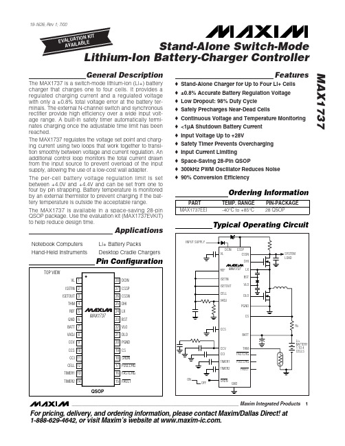
Stresses beyond those listed under “Absolute Maximum Ratings” may cause permanent damage to the device. These are stress ratings only, and functional operation of the device at these or any other conditions beyond those indicated in the operational sections of the specifications is not implied. Exposure to absolute maximum rating conditions for extended periods may affect device reliability.
Ordering Information
PART MAX1737EEI TEMP. RANGE -40°C to +85°C PIN-PACKAGE 28 QSOP
Applications
Notebook Computers Hand-Held Instruments Li+ Battery Packs Desktop Cradle Chargers
INPUT SUPPLY
Typical Operating Circuit
DCIN VL
CSSP CSSN DHI
Pin Configuration
TOP VIEW
VL 1 ISETIN 2 ISETOUT 3 THM 4 REF 5 GND 6 BATT 7 VADJ 8 CCV 9 CCS 10 CCI 11 CELL 12 TIMER1 13 TIMER2 14 28 DCIN 27 CSSP 26 CSSN 25 DHI 24 LX
TEA1733LT:GreenChip开关电源控制方案
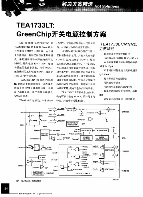
T A1 3 L / N ) E 7 3 N1 2 T (
主 要 特 性
低成本开关 电源控制器 l C 大的输入 电压范围( 2V ~3 1 0V) 在 启动和重新 启动时极低的 电流
( 常为 11 通 0 A) J
( CM ) 作 。 C 运
可调超功率重新启动定时器
频率波 动的固定开关频 率 ,降低
EMI
T A1 3 L E 7 3 T具有低成本 、 高效率 、
供 电可靠 ( 最高 7 ) L E 7 3T包 括 过 功 率 保 护 特性 ,并 且外部元件用量少。
于反激拓 扑。器件工 作在固定频 率模 管脚 留作保护之 用。其输入欠 压保护
式 ,采用 频 率 抖 动 来 降 低 电磁 干 扰 ( V ,过 电压 保 护 ( P) U P) OV ,输 出 ( MI,输入 电压 1 V 一3 V,起 动 过压保护 , E ) 2 0 和过热保护 ( P) OT 等功能 ,
配 备 安全 元 件 的 NF C功 能 手机 新的消费体验。我们将 N C技术带给 F
携 手合作 ,将恩 智浦近距 离无线通 信 能为广大 消费者提供 各种可提 高使用 消费 者 ,为他们 提供包括 电子钱包 、
( F P 5 4技术应用到中兴手机 中。 便利性和安全性 的应用程序。N C技 汽车 无钥进入 和无票交通 在 内的各种 N C) N 4 F
TEA1 3 3 7
Gre hp e n 开关 电源控 制 方案 C i
N P公 司 的 T A1 3 L/ 和 ( P) X E 7 3 TN1 OP ,这 使 得 控 制 器 在 一 定 的 H I /. ,' 3
MXP4004BTS Datasheet Dec10-13
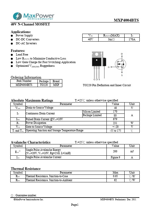
40V N-Channel MOSFETApplications:●Power Supply I D ● DC-DC Converters 170A● DC-AC InvertersFeatures:● Lead Free● Low R DS(ON) to Minimize Conductive Loss ● Low Gate Charge for Fast Switching Application ● Optimized V (BR)DSS RuggednessOrdering InformationPackage Brand TO220MXPTO220 Pin Definition and Inner CircuitAbsolute Maximum RatingsT C =25℃unless otherwise specifiedSymbolValueUnitV DSS 40V 17080I DM 679P D 231W V GS+/-20V T J and T stg-55 to 175℃Avalanche CharacteristicsT C =25℃unless otherwise specifiedSymbolValueUnitI ASFigure 9AThermal ResistanceSymbolMaxUnitR θJC 0.65℃/W R θJA62℃/WThermal Resistance, Junction-to-AmbientParameter Thermal Resistance, Junction-to-Case Power Dissipation Single Pulse Avalanche CurrentParameter A Pulsed Drain Current @V GS =10V Gate-to-Source VoltageParameter Drain-to-Source Voltage R DS(ON)(MAX)Silicon LimitedV DS 40V 3m ΩContinuous Drain CurrentPackage LimitedOperating Junction and Storage Temperature RangePark Number MXP4004BTSI DE AS ①Single Pulse Avalanche Energy(V DS =20V, V GS =10V, Rg=25Ω, L=1mH)200mJ40V N-Channel MOSFET OFF CharacteristicsT J =25℃unless otherwise specified SymbolMin Typ Max UnitV (BR)DSS 40--V --1--100--100--100ON CharacteristicsT J =25℃unless otherwise specified SymbolMin Typ Max UnitR DS(ON)- 2.33.0m ΩV GS(th)2-4VDynamic CharacteristicsT J =25℃unless otherwise specified SymbolMin Typ Max UnitCiss -5016-Coss -787-Crss -292-Qg -74-Qgs -23-Qgd -26-Td(on)-18.7-Tr -67.1-Td(off)-48.8-Tf -31-Source-Drain Diode Characteristics T J =25℃unless otherwise specifiedSymbolMinTypMaxUnitV SD -- 1.2V Trr -51.6-ns Qrr-35.1-nCGate-to-Source Charge Total Gate Charge Gate-to-Drain ("Miller") Charge Static Drain-to-Source On-ResistanceI GSSGate-to-Source Forward Leakage nAV GS =+20V Gate-to-Source Reverse LeakageV GS = -20VI DSS Drain-to-Source Leakage Current uA V DS =32V, V GS =0VV DS =32V, V GS =0V, T J =125 ℃I S =80A, V GS =0V nsV DD =20V, I D =40A,V GS =10V, R G =10Ω, R L =0.5ΩV DD =20V, I D =80A, V GS =10VTest ConditionsDrain-to-Source Breakdown VoltageV GS =0V, I D =250uA V GS =0V, V DS =20V,f=1.0MHz Output Capacitance Reverse Transfer Capacitance Parameter pFPublished by MaxPower Semiconductor Inc.V GS =10V, I D =80A ParameterTest ConditionsInput Capacitance Test ConditionsTurn-off Delay Time Fall Time Diode Forward Voltage Reverse Recovery Time Is=80A, di/dt=100A/μsReverse Recovery ChargeParameterTest ConditionsGate Threshold VoltageV GS =V DS , I D =250uATurn-on Delay Time Rise Time Parameter nC40V N-Channel MOSFET40V N-Channel MOSFET40V N-Channel MOSFETTO220Published by MaxPower Semiconductor Inc. UNIT : mm1. Outline DimensionDisclaimers:MaxPower Semiconductor Inc. (MXP) reserves the right to make changes without notice in order to improve reliability, function or design and to discontinue any product or service without notice. Customers should obtain the latest relevant information before orders and should verify that such information is current and complete. All products are sold subject to MXP's terms and conditions supplied at the time of order acknowledgement.MaxPower Semiconductor Inc., its affiliates, agents, and employees, and all persons acting on its or their behalf, disclaim any and all liability for any errors, inaccuracies or incompleteness contained herein or in any other disclosure relating to any product.MaxPower Semiconductor Inc. disclaims any and all liability arising out of the use or application of any product described herein or of any information provided herein to the maximum extent permitted by law. The product specifications do not expand or otherwise modify MXP's terms and conditions of purchase, including but not limited to the warranty expressed therein, which apply to these products.MaxPower Semiconductor Inc. warrants performance of its hardware products to the specifications at the time of sale, testing, reliability and quality control are used to the extent MXP deems necessary to support this warrantee. Except where agreed upon by contractual agreement, testing of all parameters of each product is not necessarily performed.MaxPower Semiconductor Inc. does not assume any liability arising from the use of any product or circuit designs described herein. Customers are responsible for their products and applications using MXP's components. To minimize risk, customers must provide adequate design and operating safeguards.MaxPower Semiconductor Inc. does not warrant or convey any license to any intellectual property rights either expressed or implied under its patent rights, nor the rights of others. Reproduction of information in MXP's data sheets or data books is permissible only if reproduction is without modification or alteration. Reproduction of this information with any alteration is an unfair and deceptive business practice.MaxPower Semiconductor Inc. is not responsible or liable for such altered documentation. Resale of MXP's products with statements different from or beyond the parameters stated by MaxPower Semiconductor Inc. for that product or service voids all express or implied warrantees for the associated MXP product or service and is an unfair and deceptive business practice. MaxPower Semiconductor Inc. is not responsible or liable for any such statements.Published by MaxPower Semiconductor Inc.。
常用开关电源芯片大全
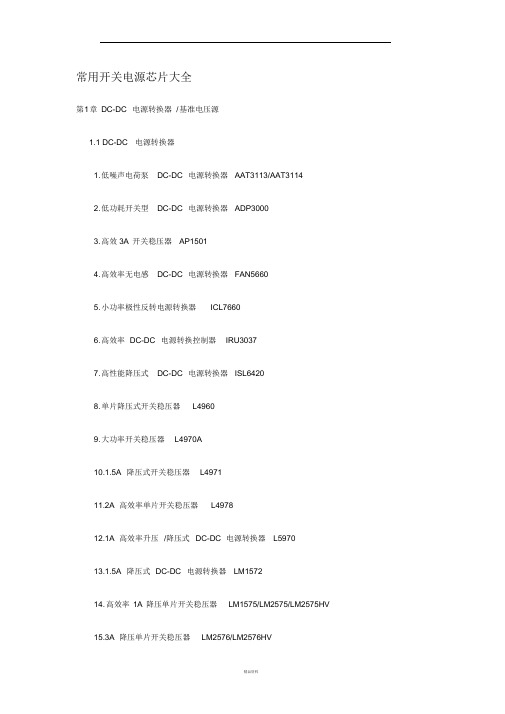
常用开关电源芯片大全第1 章DC-DC 电源转换器/ 基准电压源1.1 DC-DC 电源转换器1. 低噪声电荷泵DC-DC 电源转换器AAT3113/AAT31142. 低功耗开关型DC-DC 电源转换器ADP30003. 高效3A 开关稳压器AP15014. 高效率无电感DC-DC 电源转换器FAN56605. 小功率极性反转电源转换器ICL76606. 高效率DC-DC 电源转换控制器IRU30377. 高性能降压式DC-DC 电源转换器ISL64208. 单片降压式开关稳压器L49609. 大功率开关稳压器L4970A10.1.5A 降压式开关稳压器L497111.2A 高效率单片开关稳压器L497812.1A 高效率升压/降压式DC-DC 电源转换器L597013.1.5A 降压式DC-DC 电源转换器LM157214. 高效率1A 降压单片开关稳压器LM1575/LM2575/LM2575HV15.3A 降压单片开关稳压器LM2576/LM2576HV16. 可调升压开关稳压器LM257717.3A 降压开关稳压器LM259618. 高效率5A 开关稳压器LM267819. 升压式DC-DC 电源转换器LM2703/LM270420. 电流模式升压式电源转换器LM273321. 低噪声升压式电源转换器LM275022. 小型75V 降压式稳压器LM500723. 低功耗升/降压式DC-DC 电源转换器LT107324. 升压式DC-DC 电源转换器LT161525. 隔离式开关稳压器LT172526. 低功耗升压电荷泵LT175127. 大电流高频降压式DC-DC 电源转换器LT176528. 大电流升压转换器LT193529. 高效升压式电荷泵LT193730. 高压输入降压式电源转换器LT195631.1.5A 升压式电源转换器LT196132. 高压升/降压式电源转换器LT343333. 单片3A 升压式DC-DC 电源转换器LT343634. 通用升压式DC-DC 电源转换器LT346035. 高效率低功耗升压式电源转换器LT346436.1.1A 升压式DC-DC 电源转换器LT346737. 大电流高效率升压式DC-DC 电源转换器LT378238. 微型低功耗电源转换器LTC175439.1.5A 单片同步降压式稳压器LTC187540. 低噪声高效率降压式电荷泵LTC191141. 低噪声电荷泵LTC3200/LTC3200-542. 无电感的降压式DC-DC 电源转换器LTC325143. 双输出/低噪声/降压式电荷泵LTC325244. 同步整流/升压式DC-DC 电源转换器LTC340145. 低功耗同步整流升压式DC-DC 电源转换器LTC340246. 同步整流降压式DC-DC 电源转换器LTC340547. 双路同步降压式DC-DC 电源转换器LTC340748. 高效率同步降压式DC-DC 电源转换器LTC341649. 微型2A 升压式DC-DC 电源转换器LTC342650.2A 两相电流升压式DC-DC 电源转换器LTC342851. 单电感升/降压式DC-DC 电源转换器LTC344052. 大电流升/降压式DC-DC 电源转换器LTC344253.1.4A 同步升压式DC-DC 电源转换器LTC345854. 直流同步降压式DC-DC 电源转换器LTC370355. 双输出降压式同步DC-DC 电源转换控制器LTC373656. 降压式同步DC-DC 电源转换控制器LTC377057. 双2相DC-DC 电源同步控制器LTC380258. 高性能升压式DC-DC 电源转换器MAX1513/MAX151459. 精简型升压式DC-DC 电源转换器MAX1522/MAX1523/MAX152460. 高效率40V 升压式DC-DC 电源转换器MAX1553/MAX155461. 高效率升压式LED 电压调节器MAX1561/MAX159962. 高效率5路输出DC-DC 电源转换器MAX156563. 双输出升压式DC-DC 电源转换器MAX1582/MAX1582Y64. 驱动白光LED 的升压式DC-DC 电源转换器MAX158365. 高效率升压式DC-DC 电源转换器MAX1642/MAX164366.2A 降压式开关稳压器67. 高效率升压式DC-DC MAX1644电源转换器MAX1674/MAX1675/MAX167668. 高效率双输出DC-DC 电源转换器MAX167769. 低噪声1A 降压式DC-DC 电源转换器MAX1684/MAX168570. 高效率升压式DC-DC 电源转换器MAX169871. 高效率双输出降压式DC-DC 电源转换器MAX171572. 小体积升压式DC-DC 电源转换器MAX1722/MAX1723/MAX172473. 输出电流为50mA 的降压式电荷泵MAX173074. 升/降压式电荷泵MAX175975. 高效率多路输出DC-DC 电源转换器MAX180076.3A 同步整流降压式稳压型MAX1830/MAX183177. 双输出开关式LCD 电源控制器MAX187878. 电流模式升压式DC-DC 电源转换器MAX189679. 具有复位功能的升压式DC-DC 电源转换器MAX194780. 高效率PWM 降压式稳压器MAX1992/MAX199381. 大电流输出升压式DC-DC 电源转换器MAX61882. 低功耗升压或降压式DC-DC 电源转换器MAX62983.PWM 升压式DC-DC 电源转换器MAX668/MAX66984. 大电流PWM 降压式开关稳压器MAX724/MAX72685. 高效率升压式DC-DC 电源转换器MAX756/MAX75786. 高效率大电流DC-DC 电源转换器MAX761/MAX76287. 隔离式DC-DC 电源转换器MAX8515/MAX8515A88. 高性能24V 升压式DC-DC 电源转换器MAX872789. 升/降压式DC-DC 电源转换器MC33063A/MC34063A90.5A 升压/降压/反向DC-DC 电源转换器MC33167/MC3416791. 低噪声无电感电荷泵MCP1252/MCP125392. 高频脉宽调制降压稳压器MIC220393. 大功率DC-DC 升压电源转换器MIC229594. 单片微型高压开关稳压器NCP1030/NCP103195. 低功耗升压式DC-DC 电源转换器NCP1400A96. 高压DC-DC 电源转换器NCP140397. 单片微功率高频升压式DC-DC 电源转换器NCP141098. 同步整流PFM 步进式DC-DC 电源转换器NCP142199. 高效率大电流开关电压调整器NCP1442/NCP1443/NCP1444/NCP1445 100. 新型双模式开关稳压器NCP1501101. 高效率大电流输出DC-DC 电源转换器NCP1550102. 同步降压式DC-DC 电源转换器NCP1570103. 高效率升压式DC-DC 电源转换器NCP5008/NCP5009104. 大电流高速稳压器RT9173/RT9173A105. 高效率升压式DC-DC 电源转换器RT9262/RT9262A106. 升压式DC-DC 电源转换器SP6644/SP6645107. 低功耗升压式DC-DC 电源转换器SP6691108. 新型高效率DC-DC 电源转换器TPS54350109. 无电感降压式电荷泵TPS6050x110. 高效率升压式电源转换器TPS6101x111.28V 恒流白色LED 驱动器TPS61042112. 具有LDO 输出的升压式DC-DC 电源转换器TPS6112x113. 低噪声同步降压式DC-DC 电源转换器TPS6200x114. 三路高效率大功率DC-DC 电源转换器TPS75003115. 高效率DC-DC 电源转换器UCC39421/UCC39422116. P WM 控制升压式DC-DC 电源转换器XC6371117. 白光LED 驱动专用DC-DC 电源转换器XC9116118.500mA 同步整流降压式DC-DC 电源转换器XC9215/XC9216/XC9217 119. 稳压输出电荷泵XC9801/XC9802120. 高效率升压式电源转换器ZXLB16001.2线性/ 低压差稳压器121. 具有可关断功能的多端稳压器BAXXX122. 高压线性稳压器HIP5600123. 多路输出稳压器KA7630/KA7631124. 三端低压差稳压器LM2937125. 可调输出低压差稳压器LM2991126. 三端可调稳压器LM117/LM317127. 低压降CMOS500mA 线性稳压器LP38691/LP38693 128. 输入电压从12V 到450V 的可调线性稳压器LR8 129.300mA 非常低压降稳压器(VLDO )LTC3025 130. 大电流低压差线性稳压器LX8610131.200mA 负输出低压差线性稳压器MAX1735132.150mA 低压差线性稳压器MAX8875133. 带开关控制的低压差稳压器MC33375134. 带有线性调节器的稳压器MC33998135.1.0A 低压差固定及可调正稳压器NCP1117136. 低静态电流低压差稳压器NCP562/NCP563137. 具有使能控制功能的多端稳压器PQxx138. 五端可调稳压器SI-3025B/SI-3157B139.400mA 低压差线性稳压器SPX2975140. 五端线性稳压器STR20xx141. 五端线性稳压器STR90xx142. 具有复位信号输出的双路输出稳压器TDA8133143. 具有复位信号输出的双路输出稳压器TDA8138/TDA8138A 144. 带线性稳压器的升压式电源转换器TPS6110x145. 低功耗50mA 低压降线性稳压器TPS760xx146. 高输入电压低压差线性稳压器XC6202147. 高速低压差线性稳压器XC6204148. 高速低压差线性稳压器XC6209F149. 双路高速低压差线性稳压器XC64011.3基准电压源150. 新型XFET 基准电压源ADR290/ADR291/ADR292/ADR293 151. 低功耗低压差大输出电流基准电压源MAX610x152. 低功耗1.2V 基准电压源MAX6120153.2.5V 精密基准电压源MC1403154.2.5V/4.096V 基准电压源MCP1525/MCP1541155. 低功耗精密低压降基准电压源REF30xx/REF31xx156. 精密基准电压源TL431/KA431/TLV431A第2章AC-DC 转换器及控制器1. 厚膜开关电源控制器DP104C2. 厚膜开关电源控制器DP308P3. D PA-Switch 系列高电压功率转换控制器DPA423/DPA424/DPA425/DPA4264. 电流型开关电源控制器FA13842/FA13843/FA13844/FA138455. 开关电源控制器FA5310/FA53116. P WM 开关电源控制器FAN75567. 绿色环保的PWM 开关电源控制器FAN76018. F PS 型开关电源控制器FS6M07652R9. 开关电源功率转换器FS6Sxx10. 降压型单片AC-DC 转换器HV-2405E11. 新型反激准谐振变换控制器ICE1QS0112. P WM 电源功率转换器KA1M088013. 开关电源功率转换器KA2S0680/KA2S088014. 电流型开关电源控制器KA38xx15.FPS 型开关电源功率转换器KA5H0165R16.FPS 型开关电源功率转换器KA5Qxx17.FPS 型开关电源功率转换器KA5Sxx18. 电流型高速PWM 控制器L499019. 具有待机功能的PWM 初级控制器L599120. 低功耗离线式开关电源控制器L659021. L INK SWITCH TN 系列电源功率转换器LNK304/LNK305/LNK30622. L INK SWITCH 系列电源功率转换器LNK500/LNK501/LNK52023. 离线式开关电源控制器M51995A24. P WM 电源控制器M62281P/M62281FP25. 高频率电流模式PWM 控制器MAX5021/MAX502226. 新型PWM 开关电源控制器MC4460427. 电流模式开关电源控制器MC4460528. 低功耗开关电源控制器MC4460829. 具有PFC 功能的PWM 电源控制器ML482430. 液晶显示器背光灯电源控制器ML487631. 离线式电流模式控制器NCP120032. 电流模式脉宽调制控制器NCP120533. 准谐振式PWM 控制器NCP120734. 低成本离线式开关电源控制电路NCP121535. 低待机能耗开关电源PWM 控制器NCP123036. S TR 系列自动电压切换控制开关STR8xxxx37. 大功率厚膜开关电源功率转换器STR-F665438. 大功率厚膜开关电源功率转换器STR-G865639. 开关电源功率转换器STR-M6511/STR-M652940. 离线式开关电源功率转换器STR-S5703/STR-S5707/STR-S570841. 离线式开关电源功率转换器STR-S6401/STR-S6401F/STR-S6411/STR-S6411F 442. 开关电源功率转换器STR-S651343. 离线式开关电源功率转换器TC33369 ~TC3337444. 高性能PFC 与PWM 组合控制集成电路TDA16846/TDA1684745. 新型开关电源控制器TDA1685046. “绿色”电源控制器TEA150447. 第二代“绿色”电源控制器TEA150748. 新型低功耗“绿色”电源控制器TEA153349. 开关电源控制器TL494/KA7500/MB375950.Tiny Switch Ⅰ系列功率转换器TNY253 、TNY254 、TNY25551.Tiny Switch Ⅱ系列功率转换器TNY264P ~TNY268G52.TOP Switch (Ⅱ)系列离线式功率转换器TOP209 ~TOP22753.TOP Switch-FX 系列功率转换器TOP232/TOP233/TOP23454.TOP Switch-GX 系列功率转换器TOP242 ~T OP25055.开关电源控制器UCX84X56.离线式开关电源功率转换器VIPer12AS/VIPer12ADIP57.新一代高度集成离线式开关电源功率转换器VIPer53 第3章功率因数校正控制/节能灯电源控制器1. 电子镇流器专用驱动电路BL83012. 零电压开关功率因数控制器FAN48223. 功率因数校正控制器FAN75274. 高电压型EL 背光驱动器HV8265. E L 场致发光背光驱动器IMP525/IMP5606. 高电压型EL 背光驱动器/反相器IMP8037. 电子镇流器自振荡半桥驱动器IR21568. 单片荧光灯镇流器IR21579. 调光电子镇流器自振荡半桥驱动器IR215910. 卤素灯电子变压器智能控制电路IR216111. 具有功率因数校正电路的镇流器电路IR216612. 单片荧光灯镇流器IR216713. 自适应电子镇流器控制器IR252014. 电子镇流器专用控制器KA754115. 功率因数校正控制器L656116. 过渡模式功率因数校正控制器L656217. 集成背景光控制器MAX8709/MAX8709A18. 功率因数校正控制器MC33262/MC3426219. 固定频率电流模式功率因数校正控制器NCP165320. E L 场致发光灯高压驱动器SP440321. 功率因数校正控制器TDA4862/TDA486322. 有源功率因数校正控制器UC385423. 高频自振荡节能灯驱动器电路VK05CFL24. 大功率高频自振荡节能灯驱动器电路VK06TL第4章充电控制器1. 多功能锂电池线性充电控制器AAT36802. 可编程快速电池充电控制器BQ20003. 可进行充电速率补偿的锂电池充电管理器BQ20574. 锂电池充电管理电路BQ2400x5. 单片锂电池线性充电控制器BQ2401x6. U SB 接口单节锂电池充电控制器BQ2402x7.2A 同步开关模式锂电池充电控制器BQ241008. 集成PWM 开关控制器的快速充电管理器BQ29549. 具有电池电量计量功能的充电控制器DS277010. 锂电池充电控制器FAN7563/FAN756411.2A 线性锂/锂聚合物电池充电控制器ISL629212. 锂电池充电控制器LA5621M/LA5621V13.1.5A 通用充电控制器LT157114.2A 恒流/恒压电池充电控制器LT176915. 线性锂电池充电控制器LTC173216. 带热调节功能的1A 线性锂电池充电控制器LTC173317. 线性锂电池充电控制器LTC173418. 新型开关电源充电控制器LTC198019. 开关模式锂电池充电控制器LTC400220.4A 锂电池充电器LTC400621. 多用途恒压/恒流充电控制器LTC400822.4.2V 锂离子/锂聚合物电池充电控制器LTC405223. 可由USB 端口供电的锂电池充电控制器LTC405324. 小型150mA 锂电池充电控制器LTC405425. 线性锂电池充电控制器LTC405826. 单节锂电池线性充电控制器LTC405927. 独立线性锂电池充电控制器LTC406128. 镍镉/ 镍氢电池充电控制器M62256FP29. 大电流锂/镍镉/镍氢电池充电控制器MAX150130. 锂电池线性充电控制器MAX150731. 双输入单节锂电池充电控制器MAX1551/MAX155532. 单节锂电池充电控制器MAX167933. 小体积锂电池充电控制器MAX173634. U SB 接口单节锂电池充电控制器MAX181135. 多节锂电池充电控制器MAX187336. 双路输入锂电池充电控制器MAX187437. 单节锂电池线性充电控制器MAX189838. 低成本/多种电池充电控制器MAX190839. 开关模式单节锂电池充电控制器MAX1925/MAX192640. 快速镍镉/镍氢充电控制器MAX2003A/MAX200341. 可编程快速充电控制器MAX712/MAX71342. 开关式锂电池充电控制器MAX74543. 多功能低成本充电控制器MAX846A44. 具有温度调节功能的单节锂电池充电控制器MAX8600/MAX860145. 锂电池充电控制器MCP73826/MCP73827/MCP7382846. 高精度恒压/ 恒流充电器控制器MCP73841/MCP73842/MCP73843/MCP73844 647. 锂电池充电控制器MCP73861/MCP7386248. 单节锂电池充电控制器MIC7905049. 单节锂电池充电控制器NCP180050. 高精度线性锂电池充电控制器VM7205Welcome To Download !!!欢迎您的下载,资料仅供参考!。
南京拓微 TP4056 1 微型锂离子电池充电器数据手册说明书
南京拓微集成电路有限公司TP4056南京拓微集成电路有限公司NanJing Top Power ASIC Corp.数据手册DATASHEETTP4056(1A线性锂离子电池充电器)应用·移动电话、PDA ·MP3、MP4播放器 ·数码相机 ·电子词典 ·GPS·便携式设备、各种充电器描述 TP4056是一款完整的单节锂离子电池采用恒定电流/恒定电压线性充电器。
其底部带有散热片的SOP8/MSOP8封装与较少的外部元件数目使得TP4056成为便携式应用的理想选择。
TP4056可以适合USB 电源和适配器电源工作。
由于采用了内部PMOSFET 架构,加上防倒充电路,所以不需要外部隔离二极管。
热反馈可对充电电流进行自动调节,以便在大功率操作或高环境温度条件下对芯片温度加以限制。
充电电压固定于4.2V ,而充电电流可通过一个电阻器进行外部设置。
当充电电流在达到最终浮充电压之后降至设定值1/10时,TP4056将自动终止充电循环。
当输入电压(交流适配器或USB 电源)被拿掉时,TP4056自动进入一个低电流状态,将电池漏电流降至2uA 以下。
TP4056在有电源时也可置于停机模式,以而将供电电流降至55uA 。
TP4056的其他特点包括电池温度检测、欠压闭锁、自动再充电和两个用于指示充电、结束的LED 状态引脚。
特点 ·高达1000mA 的可编程充电电流 ·无需MOSFET 、检测电阻器或隔离二极管 ·用于单节锂离子电池、采用SOP 封装的完整线性充电器 ·恒定电流/恒定电压操作,并具有可在无过热危险的情况下实现充电速率最大化的热调节功能·精度达到±1.5%的4.2V 预设充电电压 ·用于电池电量检测的充电电流监控器输出·自动再充电 ·充电状态双输出、无电池和故障状态显示·C/10充电终止 ·待机模式下的供电电流为55uA ·2.9V 涓流充电器件版本 ·软启动限制了浪涌电流 ·电池温度监测功能 ·采用8引脚SOP-PP/MSP-PP 封装。
电源管理芯片AXP173 Datasheet
17H
38H
9.10 Host接口及中断(Host Interface and IRQ)................................................................................... 27
18H
39H
9.11 寄存器(Registers) ............................................................................................................................. 28
7.管脚定义(Pin Description)....................................................................................................................... 13
6H
27H
8.功能框图(Functional Block Diagram).................................................................................................. 15
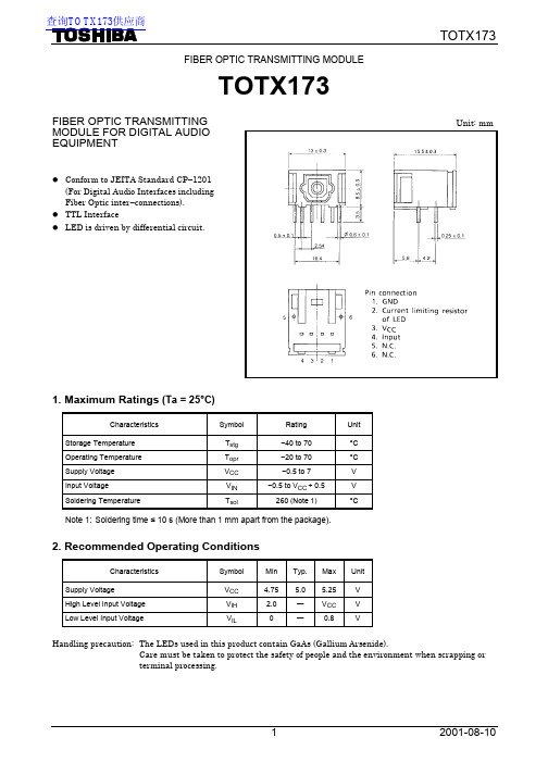
东芝 TOTX173 说明书
FIBER OPTIC TRANSMITTING MODULETOTX173FIBER OPTIC TRANSMITTING MODULE FOR DIGITAL AUDIO EQUIPMENTl Conform to JEITA Standard CP −1201(For Digital Audio Interfaces including Fiber Optic inter −connections). l TTL Interfacel LED is driven by differential circuit.1. Maximum Ratings (Ta = 25°C)Characteristics Symbol Rating UnitStorage Temperature T stg −40 to 70 °C Operating Temperature T opr −20 to 70 °C Supply Voltage V CC −0.5 to 7 V Input Voltage V IN −0.5 to V CC + 0.5 V Soldering TemperatureT sol260 (Note 1)°CNote 1: Soldering time ≤ 10 s (More than 1 mm apart from the package).2. Recommended Operating ConditionsCharacteristics Symbol Min Typ.MaxUnit Supply VoltageV CC 4.75 5.0 5.25V High Level Input Voltage V IH 2.0 ―V CCVLow Level Input VoltageV IL― 0.8 VHandling precaution: The LEDs used in this product contain GaAs (Gallium Arsenide).Care must be taken to protect the safety of people and the environment when scrapping or terminal processing.Unit: mm3. Electrical and Optical Characteristics (Ta = 25°C, V CC = 5 V)Characteristics SymbolTestConditionMinTyp.Max Unit Data Rate NRZ Code (Note 2)DC ― 6 Mb / sTransmission Distance Using APF (Note 3)and TORX1730.2 ― 10 mPulse Width Distortion (Note 4) ∆tw Pulse Width 165 nsPulse cycle 330 ns, C L = 10 p FUsing TORX173−20 ― 20 nsFiber Output Power P f APF 1 m, R = 8.2 kΩ(Note 5)−21 ―−15dBmPeak Emission Wavelength λp― 660 ― nm Current Consumption I CC R = 8.2 kΩ― 15 25 mAHigh Level Input Voltage V IH 2.0―― V Low Level Input Voltage V IL―― 0.8 V High Level Input Current I IH―― 20 µA Low Level Input Current I IL――−0.4mANote 2: LED is on when input signal is high level, it is off when low level.For data rate > 3 Mb / s, the duty factor must be kept 25 to 75%.Note 3: All Plastic Fiber (970 / 1000 µm).Note 4: Between input of TOTX173 and output of a fiber optic receiving module.Note 5: Measure with a standard optical fiber with fiber optic connectors.4. Example of Typical Characteristics (Note 6)Note 6: There give characteristic examples, and its values are not guaranteed.5. Application Circuit6. Applicable optical fiber with fiber optic connectorsTOCP 172−□□B7. Precautions during use(1) Maximum ratingThe maximum ratings are the limit values which must not be exceeded when using the device. Any one of the rating must not be exceeded. If The maximum rating is exceeded, the characteristics may not be recovered. In some extreme cases, the device may be permanently damage. (2) Life of light emittersWhen the optical module is used for over a long period, degeneration of characteristics is mostly due to lowering of the fiber output power (Pf). This is caused by the degradation of the optical output of the LED’s used as the light source. The cause of degradation of the optical output of the LED’ may be defects in wafer crystallization or mold resin stress. The detailed causes are, however, not clear.The life of light emitters is greatly influenced by operating conditions and usage environment as well as the life characteristics unique to the device. Thus, when selecting a light emitter and setting the operating conditions, Toshiba recommends that you check the life characteristics.Depending on the environment conditions, Toshiba recommends maintenance such as regular checks on the amount of optical output. (3) SolderingOptical modules use semiconductor devices internally. However, in principle, optical modules areoptical components. At soldering, take care that flux dose not contact the emitting surface or detecting surface. Also take care at flux removal after soldering.Some optical modules come with protective cap. The protective cap is used to avoid malfunction when the optical module is not in use. Not that it is not dust or waterproof.As mentioned before, optical modules are optical component. Thus, in principle, soldering where there may be flux residue or flux removal after soldering is not recommended. Toshiba recommends that soldering be performed without the optical module mounted on the board. Then, after the board is cleaned, solder the optical module manually. Do not perform any further cleaning.If the optical module cannot be soldered manually, use non −halogen (chlorine −free) flux and make sure, without cleaning, there is no residue such as chlorine. This is one of the ways to eliminate the effects of flux.(4) Vibration and shockThis module is resin −molded construction with wire fixed by resin. This structure is relatively sound against vibration or shock, In actual equipment, there are some cases where vibration, shock, and stress is applied to soldered parts or connected parts, resultingin line cut. Attention must be paid to the design of the mechanism for applications which are subject to large amounts of vibration. (5) Fixing fiber optical transceiving moduleSolder the fixed pin (pins 5 and 6) of fiber optic transmitting module TOTX 173 to the printed circuit board to fix the module to the board.(6) SolventWhen using solvent for flux removal, do not use a high acid or high alkali solvent. Be careful not to pour solvent in the optical connector ports. If solvent is inadvertently poured there, clean with cotton tips.(7) Protective capWhen the fiber optic transmitting module TOTX173 is not in use, use the protective cap.(8) Supply VoltageUse the supply voltage within the Typ. operating condition (V CC = 5 ± 0.25 V). Make sure that supply voltage does not exceed the maximum rating value of 7 V, even instantaneously.(9) Input voltageIf a voltage exceeding the maximum rating value (V CC + 0.5V) is applied to the transmitter input, the internal IC may degrade causing some damage. If excessive voltage due to surges may be added to the input, insert a protective circuit.(10) Soldering conditionSolder at 260°C or less within ten seconds.(11) Precaution on wasteWhen discarding devices and packing materials, follow procedures stipulated by local regulations in order to protect the environment against contamination.Compound semiconductors such as GaAs are used as LED materials for this module. When discarding waste or at final processing, attention must be paid to workers and the environment.(12) Precaution on useToshiba is continually working to improve the quality and the reliability of its products. Nevertheless, semiconductor devices in general can malfunction or fail due to their inherent electrical sensitivity and vulnerability to physical stress. It is the responsibility of the buyer, when utilizing Toshibaproducts, to observe standards of safety, and to avoid situations in which a malfunction or failure of a Toshiba product could cause loss of human life, bodily injury or damage to property.In developing your designs, please ensure that Toshiba products are used within specified operating ranges as set forth in the most recent product specifications. Also, please keep in mind theprecautions and conditions set forth in the Toshiba Semiconductor Reliability Handbook.· TOSHIBA is continually working to improve the quality and reliability of its products. Nevertheless, semiconductor devices in general can malfunction or fail due to their inherent electrical sensitivity and vulnerability to physical stress. It is the responsibility of the buyer, when utilizing TOSHIBA products, to comply with the standards of safety in making a safe design for the entire system, and to avoid situations in which a malfunction or failure of such TOSHIBA products could cause loss of human life, bodily injury or damage to property.In developing your designs, please ensure that TOSHIBA products are used within specified operating ranges as set forth in the most recent TOSHIBA products specifications. Also, please keep in mind the precautions and conditions set forth in the “Handling Guide for Semiconductor Devices,” or “TOSHIBA Semiconductor Reliability Handbook” etc.. · The TOSHIBA products listed in this document are intended for usage in general electronics applications (computer, personal equipment, office equipment, measuring equipment, industrial robotics, domestic appliances, etc.). These TOSHIBA products are neither intended nor warranted for usage in equipment that requires extraordinarily high quality and/or reliability or a malfunction or failure of which may cause loss of human life or bodily injury (“Unintended Usage”). Unintended Usage include atomic energy control instruments, airplane or spaceship instruments, transportation instruments, traffic signal instruments, combustion control instruments, medical instruments, all types of safety devices, etc.. Unintended Usage of TOSHIBA products listed in this document shall be made at the customer’s own risk. · Gallium arsenide (GaAs) is a substance used in the products described in this document. GaAs dust and fumes are toxic. Do not break, cut or pulverize the product, or use chemicals to dissolve them. When disposing of the products, follow the appropriate regulations. Do not dispose of the products with other industrial waste or with domestic garbage. · The information contained herein is presented only as a guide for the applications of our products. No responsibility is assumed by TOSHIBA CORPORATION for any infringements of intellectual property or other rights of the third parties which may result from its use. No license is granted by implication or otherwise under any intellectual property or other rights of TOSHIBA CORPORATION or others. · The information contained herein is subject to change without notice.000707EACRESTRICTIONS ON PRODUCT USE。
与AXP173的I2C通讯
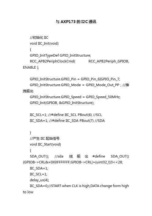
与AXP173的I2C通讯//初始化IICvoid IIC_Init(void){GPIO_InitTypeDef GPIO_InitStructure;RCC_APB2PeriphClockCmd( RCC_APB2Periph_GPIOB, ENABLE );GPIO_InitStructure.GPIO_Pin = GPIO_Pin_6|GPIO_Pin_7;GPIO_InitStructure.GPIO_Mode = GPIO_Mode_Out_PP ; //推挽输出GPIO_InitStructure.GPIO_Speed = GPIO_Speed_50MHz;GPIO_Init(GPIOB, &GPIO_InitStructure);IIC_SCL=1; //#define IIC_SCL PBout(6) //SCLIIC_SDA=1; //#define IIC_SDA PBout(7) //SDA}//产生IIC起始信号void IIC_Start(void){SDA_OUT(); //sda线输出#define SDA_OUT() {GPIOB->CRL&=0X0FFFFFFF;GPIOB->CRL|=(uint32_t)3<<28;IIC_SDA=1;IIC_SCL=1;delay_us(4);IIC_SDA=0;//START:when CLK is high,DATA change form high to lowdelay_us(4);IIC_SCL=0;//钳住I2C总线,准备发送或接收数据}//产生IIC停止信号void IIC_Stop(void){SDA_OUT();//sda线输出IIC_SCL=0;IIC_SDA=0;//STOP:when CLK is high DATA change form low to highdelay_us(4);IIC_SCL=1;IIC_SDA=1;//发送I2C总线结束信号delay_us(4);}//等待应答信号到来//返回值:1,接收应答失败// 0,接收应答成功uint8_t IIC_Wait_Ack(void){uint8_t ucErrTime=0;SDA_IN(); //SDA设置为输入#define SDA_IN() {GPIOB->CRL&=0X0FFFFFFF;GPIOB->CRL|=(uint32_t)8<<28;IIC_SDA=1;delay_us(1);IIC_SCL=1;delay_us(1);while(READ_SDA){ucErrTime++;if(ucErrTime>250){IIC_Stop();return 1;}}IIC_SCL=0;//时钟输出0 return 0;}//产生ACK应答void IIC_Ack(void) {IIC_SCL=0;SDA_OUT();IIC_SDA=0;delay_us(2);IIC_SCL=1;delay_us(2);IIC_SCL=0;}//不产生ACK应答void IIC_NAck(void) {IIC_SCL=0;SDA_OUT();IIC_SDA=1;delay_us(2);IIC_SCL=1;delay_us(2);IIC_SCL=0;}//IIC发送一个字节void IIC_Send_Byte(uint8_t txd){uint8_t t;//SDA_OUT();IIC_SCL=0;//拉低时钟开始数据传输for(t=0;t<8;t++){IIC_SDA=(txd&0x80)>>7;txd<<=1;delay_us(2);IIC_SCL=1;delay_us(2);IIC_SCL=0;//delay_us(2);}}//读1个字节,ack=1时,发送ACK,ack=0,发送nACK uint8_t IIC_Read_Byte(unsigned char ack){unsigned char i,receive=0;SDA_IN();//SDA设置为输入for(i=0;i<8;i++ ){IIC_SCL=0;delay_us(2);IIC_SCL=1;receive<<=1;if(READ_SDA)receive++;delay_us(1);}if (!ack)IIC_NAck();//发送nACKelseIIC_Ack(); //发送ACKreturn receive;}//AXP17X初始化void AXP17X_Init(void){IIC_Init();}//在AX17X指定地址读出一个数据//ReadAddr:开始读数的地址//返回值 :读到的数据uint8_t AXP17X_ReadOneByte(uint8_t ReadAddr) {uint8_t temp=0;IIC_Start();IIC_Send_Byte(0X68); //发送写命令IIC_Wait_Ack();IIC_Send_Byte(ReadAddr);//发送地址IIC_Wait_Ack();IIC_Start();IIC_Send_Byte(0X69); //进入接收模式IIC_Wait_Ack();temp=IIC_Read_Byte(0);IIC_Stop();//产生一个停止条件return temp;}//在AXP17X指定地址写入一个数据//WriteAddr :写入数据的目的地址//DataToWrite:要写入的数据void AXP17X_WriteOneByte(uint8_t WriteAddr,uint8_t DataToWrite){IIC_Start();IIC_Send_Byte(0X68); //发送写命令IIC_Wait_Ack();IIC_Send_Byte(WriteAddr);//发送地址IIC_Wait_Ack();IIC_Send_Byte(DataToWrite); //发送字节IIC_Wait_Ack();IIC_Stop();//产生一个停止条件delay_ms(10);}int main(void){delay_init();//延时函数初始化AXP17X_Init();之后就是操作AXP173的寄存器了如:AXP17X_WriteOneByte(0x26,0x32);//控制DCDC1输出2Vwhile(1){} }。
- 1、下载文档前请自行甄别文档内容的完整性,平台不提供额外的编辑、内容补充、找答案等附加服务。
- 2、"仅部分预览"的文档,不可在线预览部分如存在完整性等问题,可反馈申请退款(可完整预览的文档不适用该条件!)。
- 3、如文档侵犯您的权益,请联系客服反馈,我们会尽快为您处理(人工客服工作时间:9:00-18:30)。
8.功能框图(Functional Block Diagram) .................................................................................................. 15
7H 28H
9.控制和操作(Control and Operating) .................................................................................................... 16
19H 40H
10. 封装(Package) ........................................................................................................................................... 44
7.管脚定义(Pin Description)....................................................................................................................... 13
6H 27H
1H 2H
3.典型应用(Typical Application) ................................................................................................................. 5
2H 23H
13H 34H
9.6 多路电源输出(Multi-Power Outputs)............................................................................................. 24
14H 35H
9.7 默认电压/启动时序的设置(Default Voltage/Timing Setting) .................................................... 25
10H 31H
9.3 电源通路管理(IPS) ............................................................................................................................... 18
20H 41H
VQ.QW WPPIQPWE CC
Confidential
Page 2/45
AXP173
Enhanced single Cell Li-Battery and Power System Management IC
1.概述(Summary)
AXP173 是高度集成的电源系统管理芯片,针对单芯锂电池(锂离子或锂聚合物)且需要多路电源转换 输出的应用,提供简单易用而又可以灵活配置的完整电源解决方案,充分满足目前日益复杂的应用处理 器系统对于电源相对复杂而精确控制的要求。 AXP173 内部集成了一个自适应 USB-Compatible 的充电器, 2 路降压转换器(Buck DC-DC converter), 4 路线性稳压器(LDO),电压/电流/温度监视等多路 12-Bit ADC。为保证电源系统安全稳定,AXP173 还 整合了过/欠压(OVP/UVP)、过温(OTP)、过流(OCP)等保护电路。 AXP173 具有外部适配器和 USB 以及电池等三输入能力,其智慧电能平衡(Intelligent Power Select, IPS™)电路可以在 USB 以及外部交流适配器、锂电池和应用系统负载之间安全透明的分配电能,并且在 只有外部输入电源而没有电池(或者电池过放/损坏)的情况下也可以使应用系统正常工作。 AXP173 提供了一个与主机通讯的两线串行通讯接口:Two Wire Serial Interface (TWSI), 应用处理器可 以通过这个接口去打开或关闭某些电源输出, 设置它们的电压, 访问内部寄存器和多种测量数据(包括 Fuel Gauge)。高精度(0.5%)的电量测量数据方便消费者更清楚的实时掌握电能使用状况,给消费者带来前 所未有的设备电能使用体验。当应用系统不需要调整 AXP173 的默认输出时,它也可独立工作而无需应 用处理器的干预。 AXP173 提供 5mm x 5mm 32-pin QFN 封装。
目录 1.概述(Summary) ............................................................................................................................................ 3
15H 36H
9.8 信号采集系统(Singal Capture) ......................................................................................................... 26
16H 37H
9.9 定时器(Timer) ...................................................................................................................................... 26
8H 29H
9.1 两种工作模式(Mode Description) .................................................................................................. 16
9H 30H
9.2 开关机和复位(Power On/Off & Reset) .......................................................................................... 16
4.极限参数(Absolute Maximum Ratings) ............................................................................................... 6
3H 24H
5.电气特性(Electrical Characteristics) ....................................................................................................... 6
0H 21H
2.特性(Feature) ................................................................................................................................................ 4
管脚定义
z z
z z
VQ.QW WPPIQPWE CC
Confidential
Page 3/45
AXP173
Enhanced single Cell Li-Battery and Power System Management IC
2.特性(Feature)
• 电源管理 (IPS) o 宽输入电压范围: 2.9V~6.3V (AMR:-0.3V~11V) o 可配置的高效智慧电能平衡“IPS™”系统 o 自适应 USB 或交流适配器限压限流 (4.4V/500mA/100mA) o 内部理想二极管的等效内阻小于 100mΩ • 全集成充电器 (Charger) o 最大充电电流可达 1.4A o 支持电池温度监测 o 全面支持 USB 充电,符合规范要求 o 充电精度高,误差小于 0.5% o 支持 4.1V/4.15V/4.2V/4.36V 等多种电池 o 自动进行充电流程控制 o 可直接驱动 LED 指示充电状态 o 根据系统负载情况自动调节充电电流 • 2 路同步降压转换器 (DC-DC) o DC-DC1:可在 0.7V~3.5V 之间调节, 25mV/step, 驱动能力 1.2A o DC-DC2:可在 0.7-2.275V 之间调节, 25mV/step, 驱动能力 1.6A, 支持 VRC • 4 路线性稳压器 (LDO) o LDO1:30mA,始终有效 o LDO2: 低噪声 LDO, 1.8V~3.3V 可调节, 100mV/step, 驱动能力 200mA o LDO3:低噪声 LDO, 1.8-3.3V 可调节, 100mV/step, 驱动能力 200mA o LDO4:可在 0.7-3.5V 之间调节, 25mV/step, 驱动能力 0.5A 注:VRC,Voltage Ramp Control,电压斜 率控制。
1H 32H
9.4 自适应充电器(Adaptive Charger) ................................................................................................... 20
12H 3H
9.5 不同工作模式管脚功能区别(Mode Difference) ............................................................................. 23
