用LM3914制作通用电平显示器
lm3914工作原理
lm3914工作原理LM3914是一款常用的LED驱动芯片,它主要用于电子设备中的电平指示和模拟电平显示。
本文将介绍LM3914的工作原理,以帮助读者更好地理解和应用这一芯片。
首先,让我们来了解一下LM3914的基本结构。
LM3914是一款集成了模拟电平显示功能的集成电路芯片,它可以直接驱动LED,实现对电平的显示。
LM3914内部集成了参考电压源、比较器、LED驱动器等模块,能够根据输入的模拟电平信号控制LED的亮灭状态,从而实现电平的显示功能。
在LM3914中,输入的模拟电平信号首先经过内部的比较器进行比较,然后根据比较器的输出控制LED的亮灭状态。
LM3914具有10个LED驱动输出引脚,分别对应着10个电平显示阶段,可以根据输入信号的大小控制相应数量的LED亮起,从而实现对电平的精确显示。
LM3914的工作原理可以简单描述为,首先,输入的模拟电平信号经过内部的比较器进行比较,然后根据比较器的输出控制LED的亮灭状态,最终实现对电平的显示。
在实际应用中,用户可以通过外部电阻和电容器来调节LM3914的工作模式和显示效果,从而满足不同应用场景的需求。
除了基本的电平显示功能,LM3914还具有许多扩展功能,例如峰值保持、调光控制、外部触发模式等,这些功能使得LM3914在各种电子设备中得到广泛应用。
同时,LM3914还具有较高的精度和稳定性,能够满足对电平显示精度要求较高的应用场景。
总的来说,LM3914是一款功能强大、应用广泛的LED驱动芯片,它通过内部的比较器和LED驱动器实现对模拟电平的精确显示。
在实际应用中,用户可以根据需要调节LM3914的工作模式和显示效果,从而实现对电平的灵活显示。
希望本文能够帮助读者更好地理解和应用LM3914,为电子设备的设计和开发提供参考。
lm3914应用电路实例

lm3914应用电路实例摘要:I.引言- 介绍lm3914 应用电路实例II.lm3914 概述- 简介lm3914- 特性与功能III.lm3914 应用电路实例- 实例1:lm3914 用于led 显示驱动- 实例2:lm3914 用于vfd 显示驱动- 实例3:lm3914 用于lcd 显示驱动IV.lm3914 电路设计要点- 设计注意事项- 常见问题及解决方法V.结论- 总结lm3914 应用电路实例正文:I.引言lm3914 是一款广泛应用于电子显示领域的集成电路,它具有出色的性能和稳定性,可广泛应用于各种显示驱动电路。
本文将介绍lm3914 应用电路实例,以帮助读者更好地了解该器件在实际应用中的使用方法。
II.lm3914 概述lm3914 是由美国德州仪器公司(ti)生产的一款10 位电压比较器集成电路。
它具有以下特点:- 工作电压范围宽:3v~25v- 输出电流可调:2~30ma- 输出端承压能力强:35v- 最大输出限制在30ma 之内lm3914 可广泛应用于led、vfd 和lcd 显示驱动电路,以及各种电平表和传感器信号处理电路。
III.lm3914 应用电路实例以下是lm3914 应用电路实例:实例1:lm3914 用于led 显示驱动在led 显示驱动电路中,lm3914 通常作为level converter,用于将来自微控制器的数字信号转换为led 所需的电流。
以下是一个简单的led 显示驱动电路:```+5v ---[R1]---[D1]---[LM3914]---[R2]---[LED1]| |[RESET] [CLK]```其中,r1 和r2 分别为lm3914 的供电电阻和输出电阻,d1 为光耦合器,用于隔离微控制器的噪声。
reset 和clk 分别为复位和时钟输入,用于控制lm3914 的工作状态。
实例2:lm3914 用于vfd 显示驱动在vfd 显示驱动电路中,lm3914 通常作为电压比较器,用于检测vfd 栅极电压变化并控制vfd 的显示内容。
lm3914工作原理
lm3914工作原理LM3914是一种常用的电压级显示集成电路,广泛应用于各种电子设备中。
它具有简单的工作原理和灵活的应用方式,因此备受工程师和爱好者的青睐。
接下来,我们将详细介绍LM3914的工作原理。
LM3914的工作原理主要基于内部的10级比较器和参考电压。
它能够将输入电压转换为相应的LED或LCD显示,从而实现电压级的直观显示。
在使用LM3914时,我们首先需要确定输入电压的范围,并选择合适的参考电压。
然后,通过外部电阻的连接,将输入电压与参考电压进行比较,从而确定LED或LCD的亮度。
LM3914内部包含10个比较器,它们将输入电压与参考电压进行比较,并控制相应的LED或LCD显示。
当输入电压超过某一比较器的阈值时,相应的LED或LCD将被点亮,从而直观地显示出当前的电压级。
通过调整参考电压和外部电阻的数值,我们可以灵活地控制显示的范围和精度。
除了基本的电压级显示功能,LM3914还具有峰值保持和线性/对数显示等特性。
峰值保持功能能够在输入电压波动时,保持LED或LCD显示的最大值,从而更好地反映电压的变化。
而线性/对数显示则能够根据实际需求,选择线性或对数的显示方式,使得显示效果更加符合实际应用场景。
在实际应用中,LM3914可以广泛用于电源电压显示、音频电平显示、电池电量显示等场合。
通过合理的电路设计和参数选择,我们可以实现各种不同的显示要求,从而满足不同领域的应用需求。
总的来说,LM3914作为一种电压级显示集成电路,具有简单的工作原理和灵活的应用方式。
它通过内部的比较器和参考电压,实现了输入电压到LED或LCD显示的转换,从而方便地实现电压级的直观显示。
在实际应用中,我们可以根据具体的需求,灵活选择参数和电路设计,从而实现各种不同的显示效果。
LM3914的出现,为电子设备的显示功能提供了便利和灵活性,也为工程师和爱好者们的创意和设计带来了更多的可能性。
lm3914应用电路实例
lm3914应用电路实例
【最新版】
目录
1.LM3914 概述
2.LM3914 的工作原理
3.LM3914 的应用电路实例
4.LM3914 的注意事项
正文
LM3914是一种点/条显示驱动集成电路,由美国NS公司研制。
它内部包含输入缓冲器、10级精密电压比较器、1.25V基准电压源及点/条显示方式选择电路等。
10级电压比较器的同相输入端与电阻分压器相连,电阻分压器由10只1kg精密电阻串联组成。
各单位级比较器的加权值相等,从而使得十级线性显示驱动器的组成,适合与LED显示屏、LCD显示屏和VFD电平表等设备使用。
LM3914 的工作原理是通过内部的 10 级精密电压比较器对输入电压进行比较,并将比较结果输出。
电阻分压器由 10 只 1kg 精密电阻串联组成,使得各单位级比较器的加权值相等。
这样就可以实现十级线性显示驱动器,适合与各种显示设备相连。
此外,LM3914 的工作电压范围为
3V~25W,最高可达 48V,输出电流在 2~30mA 范围可调,输出端承压能力为 35V,最大输出限制在 30mA 之内。
LM3914 的应用电路实例主要包括 LED 显示屏、LCD 显示屏和 VFD 电平表等。
它可以通过电阻分压器和电压比较器实现对显示设备的驱动,从而实现点/条显示。
在使用 LM3914 时,需要注意其工作电压、输出电流等参数,以保证其在应用中的稳定性和可靠性。
总之,LM3914 是一种具有广泛应用的点/条显示驱动集成电路,适用于 LED 显示屏、LCD 显示屏和 VFD 电平表等设备。
lm3914工作原理
lm3914工作原理LM3914是一款常用的LED驱动芯片,广泛应用于电子测量仪器、音频电平指示器、电池状态指示器等领域。
它是一款集成了模拟电压比较器、参考电压源和LED驱动器的专用集成电路,可以方便地实现LED的电平指示功能。
那么,LM3914是如何工作的呢?接下来,我们将详细介绍LM3914的工作原理。
首先,我们来看一下LM3914的基本工作原理。
LM3914内部包含了10个比较器,这些比较器可以将输入的模拟电压与内部的参考电压进行比较。
当输入电压超过了参考电压时,对应的LED将被点亮,从而实现电平指示的功能。
在LM3914内部,有一个10级的电压分割器,用于将输入电压分成10个等级,并且每个等级对应一个LED的点亮状态。
因此,LM3914可以根据输入电压的大小,点亮相应数量的LED,从而实现电平的指示。
其次,我们来分析LM3914的工作原理。
当输入电压超过了参考电压时,对应的比较器输出高电平,从而点亮相应的LED。
而当输入电压低于参考电压时,比较器输出低电平,LED则被熄灭。
通过这种方式,LM3914可以根据输入电压的大小,动态地控制LED的亮灭状态,实现电平的精准指示。
此外,LM3914还具有内部的电流调节功能,可以根据外部电阻的设置,调节LED的亮度。
这使得LM3914可以适应不同环境下的亮度要求,从而更好地满足用户的需求。
总的来说,LM3914的工作原理非常简单而又实用。
通过内部的比较器和参考电压源,可以实现对输入电压的精准比较,并控制LED的点亮状态。
同时,内部的电流调节功能也为用户提供了更大的灵活性。
因此,LM3914在电子测量仪器、音频电平指示器、电池状态指示器等领域具有广泛的应用前景。
综上所述,LM3914是一款功能强大、性能稳定的LED驱动芯片,其工作原理简单而又实用。
通过对输入电压的比较,可以精准地控制LED的点亮状态,从而实现电平的指示。
希望本文对您了解LM3914的工作原理有所帮助。
lm3914工作原理
lm3914工作原理LM3914是一种集成电路,被广泛应用于电子仪器和设备中,其工作原理是将电压转换为模拟或数字的显示输出。
LM3914是一种线性电压级联显示器,具有10个输出级别,每个级别对应一个LED 指示灯。
我们来了解一下LM3914的基本结构和内部组成。
LM3914包含一个10级比较器,一个电流源以及一个模拟开关。
其中,比较器用于将输入电压与参考电压进行比较,并根据比较结果控制LED的亮度。
电流源则用于提供恒定的电流,以确保LED的亮度稳定。
模拟开关则用于根据比较结果控制LED的亮灭。
LM3914的工作原理是基于比较器的运作。
比较器接收输入电压和参考电压,并将比较结果输出。
当输入电压大于参考电压时,比较器输出高电平;当输入电压小于参考电压时,比较器输出低电平。
LM3914的10个比较器按照从低到高的顺序排列,每个比较器的参考电压都不同。
因此,根据输入电压与不同参考电压的比较结果,可以确定输入电压所对应的LED指示灯的亮度。
LM3914还具有可调的参考电压和亮度级别控制功能。
通过调节参考电压,可以改变LED的亮度范围。
通过调节亮度级别控制引脚,可以选择显示输出的级别数量。
LM3914还具有内部对数放大器,用于将输入电压转换为对数形式的输出,以实现更精确的显示。
LM3914的应用范围非常广泛。
例如,在音频设备中,可以使用LM3914将输入音频信号的强度转换为LED指示灯的亮度,实现音频信号的可视化。
在电源管理系统中,可以使用LM3914将电池电压转换为LED指示灯的亮度,以显示电池的剩余电量。
在工业控制系统中,可以使用LM3914将传感器输出的模拟信号转换为LED指示灯的亮度,以便操作员对系统状态进行监控。
总结起来,LM3914是一种基于比较器的线性电压级联显示器,通过将输入电压与参考电压进行比较,控制LED的亮度。
它具有可调的参考电压和亮度级别控制功能,广泛应用于电子仪器和设备中,实现电压到显示输出的转换。
LM3914音乐电平制作讲解教程

自制LED音乐电平详细教程(图解)
制作初衷:
许多朋友都喜欢闲暇的时候放开音响听听动感的音乐来解闷,我也不例外,突然有一天注意到音响上的电源指示灯随音量的高低闪烁变动,极为好看。
我清楚这是音量太大,音响稳压器过载的结果,但是如果能单独有这么个东西该多好,于是我就在网上乱搜结果还真的有,一开始以为非常复杂,没想到有人能亲收制作,于是我就有了一个计划自制一个LED音乐电平。
首先电路图必须有,我不是学电子的,所以搜的
这是10个LED组成的音乐电平电路图,
其次就是选购材料和工具了,在西安电子大楼和中工电子市场转,想要什么就有什么,需要的材料主要有
1.白发蓝LED 50只(实际用20只预防烧掉和其他用途)。
2.试验面包板.链接线一套。
3.稳压电源(3~12V)一个。
4.耳机分支器一个。
5.电位器5K两个。
6.PCB板(40*60cm)。
7.小开关一个。
8.芯片插座和芯片LM3914两个。
9.耳机插孔
10.导线若干。
11.电烙铁焊锡支架焊线等工具。
严格按照电路图在面包试验板上链接好,然后就上电脑耳机输出口通电,试验几次不成功,问了电子电工实训的老师结果是电源没接对,切记这里的三根线,Vcc和Vled 是接电源的正极,GND 是接地也就是负极了。
最后成功了
因为10个LED太少了长度不够,感觉不是很明显,所以就串联一个相同的。
在PCB板上焊好电路
最后挂在墙上配上优美的DJ曲美即了
中国西安。
[图]LED通用电平显示电路 电路图
![[图]LED通用电平显示电路 电路图](https://img.taocdn.com/s3/m/4309d353f7ec4afe04a1dfe8.png)
[图]LED通用电平显示电路电路图[图]LED通用电平显示电路利用10个发光二极管作为输入端电平变化的显示,输入端电平信号可以是通过各类传感器和变换电路而探测的各种物理量,如电压、电流、温度、湿度、亮度、响度、音频、距离、磁场强度、重量等等。
用它做成的电平显示器,既醒目、直观,又方便、实用,并且能反映瞬间变化的信号,用途十分广泛。
例如,在电路设计制作中,它既可以通过探头和处理电路实现温度控制和显示,用于烘箱、冰箱、空调、热塑封机等设备上,也可以通过分压变换电路实现电压高低的直观显示,用于仪器、仪表、音响及办公设备上。
核心电路采用了塑封双列直插的18脚LED点条显示驱动集成电路LM3914,电路构成及管脚功能如图1 所示。
LM3914内部含有10个相同的电压比较器,它们的输出端可以分别直接驱动外接的10只发光二极管(VDl—VDl0)作条状显示,也可以实现点状显示。
它们的反相输入端并联在一起,并通过一个缓冲器接到输入端⑤脚。
而10个同相输入端分别接到由10个精密电阻串联而成的多级分压器上。
而这个分压器的两端在内部没有与其它电路或公共端相连,而是直接由⑥、④脚引出,通常将之称为悬浮式,这样使得应用电路的设计更加灵活和方便。
此集成电路内部还包含一个悬浮式1.25V的标准电压源,直接由⑦、⑧脚引出。
分压器两端⑥、④脚即可直接接1.25V的标准电压源,也可外接设定的其它电压值。
点状或条状显示的选择方式为:⑨、(11)脚相接(或⑨脚悬空)为点状显示,⑨、③脚相接为条状显示。
LM3914的电源电压范围很宽,可在3—18V范围内选择,实际应用中,通常取6—12V。
模拟信号由⑤脚输入,并经内部高输入阻抗缓冲器后加至内部10级电压比较器的反相输入端,每级电压比较器的同相输入端被一串分压电阻偏置在不同的比较电平上。
由于分压电阻均为1kΩ,故10级比较器的进位电平呈线性变化。
当④脚接地。
⑥与设定的基准电压UO相连(当然也可相连内部的1250mV的基准电压输出端⑦脚)每级分压器上的电压均为1\10 UO。
制作LM3914汽车电压显示器电路板
酒泉职业技术学院毕业设计(论文)08 级汽车检测与维修专业题目:制作LM3914汽车电压显示器电路板毕业时间:二O一O年六月学生姓名:指导教师:班级:08汽修班2010年11月20日酒泉职业技术学院2008 届各专业毕业论文(设计)成绩评定表说明:1、以上各栏必须按要求逐项填写.。
2、此表附于毕业论文(设计)封面之后。
目录摘要 (4)一、设计目的 (5)二、补充安装说明 (5)三、添加元件库 (6)四、编辑元件 (7)五、电路原理图的设计 (8)1.电路原理图的设计 (8)2.产生网络表 (9)3.印制电路板的设计 (9)六、绘制简单电路图 (9)七、电路板设计规则和限制 (10)1.电路板制成 (10)2.电路板厚度尺寸 (11)3.进行Protel DXP手工布局时,遵循的规则 (11)4.布线之规则 (12)5.高频布线 (14)6.焊盘设计 (15)7.填充 (16)8.跨接线 (16)9.接地 (16)10.抗干扰 (17)11.三维视图 (17)12.结构图 (19)心得体会 (20)参考文献 (21)摘要:Protel99se简介随着计算机软硬件技术的飞速发展,集成电路被广泛应用,电路越来越复杂,集成电路越来越高,加之元器件层出不穷,使得越来越多的工作已经无法依靠手工来完成。
计算机广泛应用恰恰解决了这个问题,并且大大提高了工作效率。
因此,计算机辅助电路板设计已经成为电路板设计制作的必然趋势。
Protel系列软件早期版本用于设计pcb,后来增加了绘制电路原理图的功能,再后来又增加了电路仿真功能和可编程器件开发功能。
主要有原理图设计系统、印制电路板设计系统两大部分组成。
本文主要介绍了以PCB板制作LM3914汽车电压显示器电路板的基本过程,以及制作的整体思路和在制作的过程应注意的地方,本PCB板涉及到了元件原理图绘制、元件原理图和元件封装图之间、原理图管脚和元件封装图焊盘之间的关系、设计环境的颜色的变化、PCB板层的设置方法与电路板尺寸的确定方法及对象属性的编辑方法。
利用条图显示驱动器LM3914组成100段LED显示器的方法
利用条图显示驱动器LM3914组成100段LED显示器的方
法
滕子拓
【期刊名称】《电子技术应用》
【年(卷),期】1993(0)12
【摘要】从LM3914的基本原理出发,介绍如何用动态扫描技术实现100段LED条图显示器。
这种条图显示仪表是继数字显示仪表之后出现的一种新型显示仪表。
【总页数】3页(P38-40)
【作者】滕子拓
【作者单位】无
【正文语种】中文
【中图分类】TN873
【相关文献】
1.显示驱动器LM3914及其在锅炉模拟仿真系统中的应用 [J], 陈卫红;胡长松
2.多功能LED光柱显示驱动器—LM3914 [J], 许彦斌
3.LED点/条显示驱动器LM3914/15/16 [J], 周传伟
4.利用FPGA的全彩OLED显示器控制电路 [J], 邱欣;徐奕斐;余峰;黄浩;孙鸣
5.基于卫星影像制作土地利用和土地覆盖图的方法试验——全国1∶5万土地利用/土地覆盖图制作试验项目 [J], 王旭红
因版权原因,仅展示原文概要,查看原文内容请购买。
lm3914应用电路实例
LM3914应用电路实例引言LM3914是一款广泛应用于电子仪器仪表和音频显示等领域的集成电路芯片。
它能够将模拟信号转换为二级制代码,并通过内部的10级LED(Light Emitting Diodes)驱动器来显示不同的信号强度。
LM3914可以方便地用于设计各种指示灯、电子音量控制和电平显示等应用。
LM3914基础知识在了解如何应用LM3914之前,先来了解一些LM3914的基础知识。
LM3914具有10个LED指示灯,可以通过外部电阻调整驱动电流。
该芯片还包含了内部电流放大器,用于放大输入信号的电压范围。
在芯片上,有一条分隔的参考电压线,用于定义LED指示灯之间的亮度差距。
LM3914有两种驱动模式:点对点驱动(Dot Mode)和线性条(Bar Mode)。
点对点驱动模式将所有LED以点亮的方式显示,并且只有一个LED会被点亮,所显示的位置取决于输入信号的强度。
线性条模式则是通过点亮多个LED并连成一条线的方式表示输入信号的强度。
我们需要根据具体的应用场景来选择合适的驱动模式。
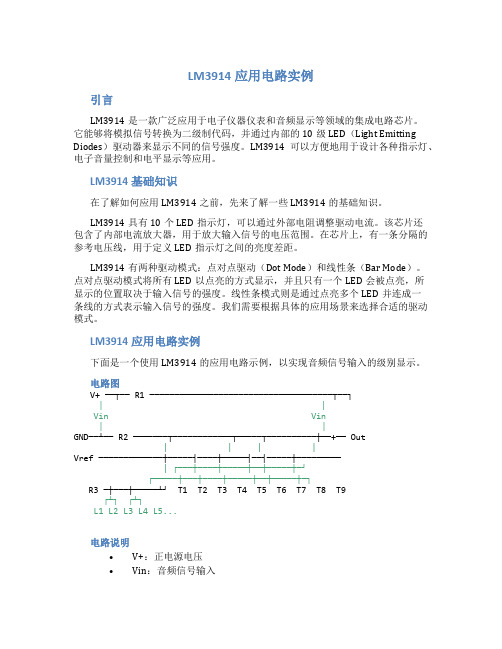
LM3914应用电路实例下面是一个使用LM3914的应用电路示例,以实现音频信号输入的级别显示。
电路图V+ ──┬── R1 ─────────────────────────────────────┬──┐│ │Vin Vin│ │GND──┴── R2 ───────┬────────────┬─────┬──────────┼──+── Out| | | |Vref ─────────────┼─────┤────┼─────┤──┤─────┼─────────| ┌───┼────┼─────┼──┼─────┼─┘┌─────┼───┼────┼─────┼──┼─────┼─┐R3 ─┼───┼─────┴┘ T1 T2 T3 T4 T5 T6 T7 T8 T9┌┴┐ ┌┴┐L1 L2 L3 L4 L5...电路说明•V+:正电源电压•Vin:音频信号输入•GND:接地•Vref:参考电压•Out:LM3914的输出引脚•R1:电流放大器的限制电阻•R2:输入信号的放大电阻•R3:将一个电位器与Vin连接来调整Vin的增益•L1-L9:LM3914驱动的LED指示灯工作原理在这个电路中,音频信号输入通过R2和C1与Vin相连。
lm3914工作原理
lm3914工作原理LM3914是一种广泛应用于电子测量和显示的集成电路,它能够将模拟信号转换为数字显示。
在本文中,我们将深入探讨LM3914的工作原理,以便更好地理解其在电子领域中的应用。
LM3914是一种由National Semiconductor(现在是德州仪器)生产的集成电路,它是一种模拟电压显示驱动器,能够将模拟信号转换为10个LED的亮度级别。
LM3914内部集成了一个精密的参考电压源、一个精密的电压比较器和一个计数器/分频器。
它可以通过外部电阻和电压源来调整亮度级别和显示范围。
LM3914的工作原理非常简单,它通过对输入信号进行比较,然后控制LED的亮度来显示输入信号的大小。
当输入信号超过设定的阈值时,相应的LED将点亮,从而实现对输入信号的可视化显示。
在LM3914内部,有10个电压比较器,它们可以分别比较输入信号与参考电压的大小,然后控制对应LED的亮度。
LM3914的工作原理可以通过以下步骤来解释,首先,输入信号通过电阻网络传递到LM3914的引脚,然后被内部的电压比较器逐个比较。
当输入信号超过某个电压比较器的阈值时,该电压比较器输出高电平,从而点亮相应的LED。
通过调整电阻网络和参考电压源,可以实现对输入信号的精确显示和调节。
LM3914广泛应用于电子测量仪器、音频设备、电源显示、电池状态显示等领域。
它不仅能够实现对输入信号的直观显示,还可以通过外部电路实现更复杂的功能,比如峰值保持、信号平均、滤波等。
由于其简单的工作原理和灵活的应用,LM3914受到了广泛的欢迎。
总的来说,LM3914是一种非常实用的集成电路,它通过简单而有效的工作原理,实现了对模拟信号的数字显示。
通过本文的介绍,相信大家对LM3914的工作原理有了更深入的理解,希望能够为大家在电子领域的应用提供一些帮助。
LM3914的工作原理虽然简单,但是在实际应用中却有着丰富的可能性,希望大家能够通过不断的实践和探索,发挥其最大的潜力。
酒精传感器实验报告
课程:传感器应用班级:12物联网姓名:学号:指导老师:一、实验名称:酒精传感器二、实验目的:1、能够读懂电子产品原理图,了解气敏传感器以及各电子元件的作用。
2、能够具备电子产品的焊接技能以及故障分析、判断能力。
三、功能描述:本设计介绍了一种酒精浓度检测仪的设计方法,主要利用MQ3还原性气体传感器作为酒精气体传感器,通过分压电阻转换为成比例的电压,再利用线性显示驱动LM3914驱动不同颜色的发光二极管和蜂鸣器提示检测得到的酒精浓度大小。
根据自动检测系统的组成结构,该酒精浓度检测仪包含酒精气体传感器,信号处理电路和执行指示机构等部分。
对于酒精气体传感器,只要是一般性的还原性气体传感器都能够使用。
具体的信号传递与结构如下图所示。
四、硬件电路设计:电路的前端部分MQ3传感器和分压电路按照常规设计即可,执行驱动声光指示的电路需要驱动多个发光管以及一个蜂鸣器,即需要将分压电路得出的电压转换成LED线段显示同时在某点驱动蜂鸣器发声。
因此本设计拟采用LED通用电平显示驱动芯片LM3914作为执行机构。
1、MQ-3气敏电阻传感器本设计采用的是表面电阻控制型气敏传感器MQ-3,该气体传感器的敏感材料是活性很高的金属氧化物半导体,最常用的如SnO2。
金属氧化物半导体在空气中被加热到一定温度时,氧原子被吸附在带负电荷的半导体表面,半导体表面的电子会被转移到吸附氧上,氧原子就变成了氧负离子,同时在半导体表面形成一个正的空间电荷层,导致表面势垒升高,从而阻碍电子流动,电阻较大。
当N 型半导体的表面在高温下遇到离解能力较小(易失去电子)的还原性气体时,气体分子中的电子将向气敏电阻表面转移,使气敏电阻中的自由电子浓度增加,电阻率降低,电阻减小。
其应用于家庭、工厂、商业场所的气体泄漏监测装置,防火/安全探测系统。
气体泄漏报警器,气体检漏仪。
特点:高灵敏度、快速响应恢复、优异的稳定性、长寿命、驱动电路简单、电信号输出强。
如下图所示。
lm3914应用电路实例

LM3914应用电路实例
一个常见的LM3914应用电路是LED音频电平指示器。
该电路可以将音频信号的强度与LED灯的亮度相对应,用于显示音频信号的音量级别。
以下是一个简单的LM3914应用电路实例:
首先,需要将音频信号通过一个电容耦合到LM3914的引脚5 (IN-)和引脚6 (IN+)之间。
电容值通常选择10uF。
接下来,将引脚9 (REF OUT)与引脚4 (RHI)连接,并通过一个电阻连接到正电源。
然后,将引脚7 (RLO)连接到地。
然后,将引脚3 (VLED)连接到正电源。
接下来,需要连接一个电阻网络,用于设置显示级别和LED亮度。
这个电阻网络由引脚2 (RHI) 和引脚8 (VLED)之间的电阻组成。
这些电阻值需要根据具体需求进行选择。
可以使用LM3914的数据手册中提供的电阻值表来帮助选择正确的电阻值。
最后,将引脚1 (GND)、引脚11 (LEDBAR)和引脚10 (MODE)连接到适当的控制器或电源。
这样,当音频信号的强度变化时,LED灯的亮度也会相应地变化,从而实现LED音频电平指示器的功能。
请注意,这只是一个简单的LM3914应用电路示例。
具体的应用电路可能会根据具体需求和使用场景而有所不同。
建议参考LM3914的数据手册和应用笔记来获取更多详细信息和更多应用电路示例。
LM3914中文资料
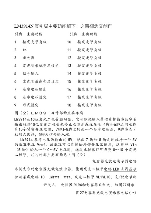
LM3914N 其引脚主要功能如下:之青柳念文创作引脚 主要功能 引脚 主要功能1 接发光管负极 10 接发光管负极2 地 11 接发光管负极3 正电源 12 接发光管负极4 发光管最低亮度设定 13 接发光管负极5 信号输入 14 接发光管负极6 发光管最高亮度设定 15 接发光管负极7 基准电压输出 16 接发光管负极8 基准电压设定 17 接发光管负极9 形式设定 18 接发光管负极图(2)LM3914外部的主要布局LM3914是10位发光二极管驱动器,它可以把输入摹拟量转换为数字量输出驱动10位发光二极管来停止点显示或柱显示.4脚和6脚之间毗连有10个紧密分压电阻,7脚和8脚之间是一个参考电压源,9脚为点/柱形式选择,5脚为信号输入端.LM3914参考电压源输出约5V ,即在7脚和8脚之间维持一个5V 的基准电压Vref ,该基准可以直接给外部分压器使用,这样当Vin (5脚)输入一个0~5V 电压时,通过比较器即可点亮0~10个发光二极管,芯片外部主要布局见上图(2).电容器充放电演示器电路线显示点LED 电路二极管本例先容的电容器充放电演示器,能用发光放电节制/、充VL1VLlO 发光二极管、????????LM IC 集成电路驱动开关S 、 电阻器RlR4和电容器C 组成,如图27所示.图27电容器充放电演示器电路(一)LM3914外部由输入缓冲器、10级电压比较器 (由分压器和比较器组成)、显示摹拟选择电路、1.25V基准电源电路等组成.摹拟信号从其5脚 (输入端)加入,经输入缓冲器放大后,送至10级电压比较器的反相输出端,与各电压比较器正相输大端的分压器上基准电压停止比较.每级分压器上的基准电压为0.125V,逐级比较电平分别为0.125V、0.25V、0.375V、0.5V…1.25V.当输入摹拟信号电压低于0.125V时,10级比较器均输出高电平;当输入信号电压高于0.125V 时,电压比较器1输出低电平 (1脚);当输入信号电压高于0.25V时,电压比较器2输出低电平 (18脚)…当输入信号电压高于1.25V时,电压比较器10输出低电平 (10脚).若将这10个输出端接上发光二极管,即可线性地显示出输大摹拟信号的大小.LM3914的9脚为显示形式转换端,将该脚接地或悬空时,显示形式为点状 (LED单级发光);•将该脚接正电源端 (Vcc)时,显示形式为线状 (逐级发光).该电容器充放电演示器电路为线状显示形式.演示时,将充/放电选择开关S拨至 "1"位置,+6V电压经S和•Rl对电容器C充电,使IC的5脚电压逐渐上升,lC内l0个电压比较器的输出端依次输出低电平,VLlVLlO 逐个被点亮,演示了电容器充电过程.将S置于"2"位置时,C无放电回路,IC的5脚电压和各输出端电压不变,VLlVLlO点亮的数量维持不变,标明电容器有存储电能的特性.将S置于"3"位置时,C颠末RI 对地放电,使IC的5脚电压逐渐下降,10个电压比较器的输出端又依次输出高电平,VLlO、VLg…VLl逐个熄灭,演示了电容器放电过程.更换分歧容量的电容器或改变Rl的阻值,可以改变电容器的充放电时司常数,从而改变VLlVLlO点亮的速度及时间长短. 元器件选择RlR4均选用1/4W或l/8W碳膜电阻器. C选用耐压值为16V的铝电解电容器. VLlVLlO均选用p5mm或p8mm的高亮度发光二极管. S选用单极三位拨动式开关.两块LM3914构成的20位LED点/线转换显示电路。
用LM3914制作通用电平显示器
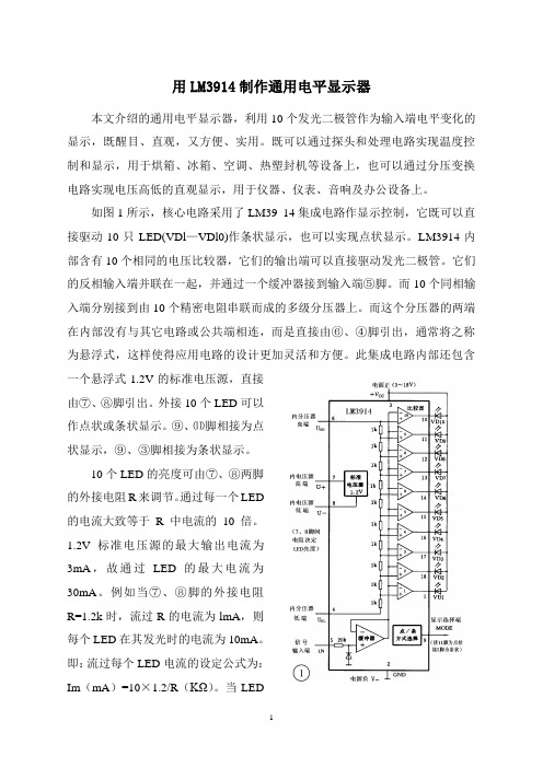
用L M3914制作通用电平显示器本文介绍的通用电平显示器,利用10个发光二极管作为输入端电平变化的显示,既醒目、直观,又方便、实用。
既可以通过探头和处理电路实现温度控制和显示,用于烘箱、冰箱、空调、热塑封机等设备上,也可以通过分压变换电路实现电压高低的直观显示,用于仪器、仪表、音响及办公设备上。
如图1所示,核心电路采用了LM39 14集成电路作显示控制,它既可以直接驱动10只LED(VDl—VDl0)作条状显示,也可以实现点状显示。
LM3914内部含有10个相同的电压比较器,它们的输出端可以直接驱动发光二极管。
它们的反相输入端并联在一起,并通过一个缓冲器接到输入端⑤脚。
而10个同相输入端分别接到由10个精密电阻串联而成的多级分压器上。
而这个分压器的两端在内部没有与其它电路或公共端相连,而是直接由⑥、④脚引出,通常将之称为悬浮式,这样使得应用电路的设计更加灵活和方便。
此集成电路内部还包含一个悬浮式1.2V的标准电压源,直接由⑦、⑧脚引出。
外接10个LED可以作点状或条状显示。
⑨、⑾脚相接为点状显示,⑨、③脚相接为条状显示。
10个LED的亮度可由⑦、⑧两脚的外接电阻R来调节。
通过每一个LED的电流大致等于R中电流的10倍。
1.2V标准电压源的最大输出电流为3mA,故通过LED的最大电流为30mA。
例如当⑦、⑧脚的外接电阻R=1.2k时,流过R的电流为lmA,则每个LED在其发光时的电流为10mA。
即:流过每个LED电流的设定公式为:Im(mA)=10×1.2/R(KΩ)。
当LED的发光效率较高时,电流可以小一些,以降低功耗。
下面以一个分辨率为0.12V的10级线性电压表为例说明其工作原理。
这个电压表的最大量程为 1.2v,将⑨、⑾脚相连,设定为点状显示,这样比较省电。
分压器就用内部基准电压源,⑥、⑦脚相连,④、⑧脚相连并接地,则分压器每个1K电阻上的压降为0.12V,因此最下面的一个比较器1同相输入端的电位为0.12V,比较器2同相输入端电位为0.24V,依此类推,最上面的一个比较器10基准电压设定为1.2V。
LM3914
LM3914Dot/Bar Display Driver General DescriptionThe LM3914is a monolithic integrated circuit that senses analog voltage levels and drives10LEDs,providing a linear analog display.A single pin changes the display from a moving dot to a bar graph.Current drive to the LEDs is regulated and programmable,eliminating the need for resis-tors.This feature is one that allows operation of the whole system from less than3V.The circuit contains its own adjustable reference and accu-rate10-step voltage divider.The low-bias-current input buffer accepts signals down to ground,or V−,yet needs no protection against inputs of35V above or below ground.The buffer drives10individual comparators referenced to the precision divider.Indication non-linearity can thus be held typically to1⁄2%,even over a wide temperature range. Versatility was designed into the LM3914so that controller, visual alarm,and expanded scale functions are easily added on to the display system.The circuit can drive LEDs of many colors,or low-current incandescent lamps.Many LM3914s can be“chained”to form displays of20to over100seg-ments.Both ends of the voltage divider are externally avail-able so that2drivers can be made into a zero-center meter. The LM3914is very easy to apply as an analog meter circuit. A1.2V full-scale meter requires only1resistor and a single 3V to15V supply in addition to the10display LEDs.If the1 resistor is a pot,it becomes the LED brightness control.The simplified block diagram illustrates this extremely simple external circuitry.When in the dot mode,there is a small amount of overlap or “fade”(about1mV)between segments.This assures that at no time will all LEDs be“OFF”,and thus any ambiguous display is avoided.Various novel displays are possible.Much of the display flexibility derives from the fact that all outputs are individual,DC regulated currents.Various effectscan be achieved by modulating these currents.The indi-vidual outputs can drive a transistor as well as a LED at thesame time,so controller functions including“staging”controlcan be performed.The LM3914can also act as a program-mer,or sequencer.The LM3914is rated for operation from0˚C to+70˚C.TheLM3914N-1is available in an18-lead molded(N)package.The following typical application illustrates adjusting of the reference to a desired value,and proper grounding for ac-curate operation,and avoiding oscillations.Featuresn Drives LEDs,LCDs or vacuum fluorescentsn Bar or dot display mode externally selectable by usern Expandable to displays of100stepsn Internal voltage reference from1.2V to12Vn Operates with single supply of less than3Vn Inputs operate down to groundn Output current programmable from2mA to30mAn No multiplex switching or interaction between outputsn Input withstands±35V without damage or false outputsn LED driver outputs are current regulated,open-collectorsn Outputs can interface with TTL or CMOS logicn The internal10-step divider is floating and can bereferenced to a wide range of voltagesFebruary2003LM3914Dot/BarDisplayDriver©2004National Semiconductor Corporation Typical Applications0V to 5V Bar Graph Meter00797001Note:Grounding method is typical of all uses.The 2.2µF tantalum or 10µF aluminum electrolytic capacitor is needed if leads to the LED supply are 6"or longer.L M 3914 2Absolute Maximum Ratings(Note1)If Military/Aerospace specified devices are required, please contact the National Semiconductor Sales Office/ Distributors for availability and specifications.Power Dissipation(Note6)Molded DIP(N)1365mW Supply Voltage25V Voltage on Output Drivers25V Input Signal Overvoltage(Note4)±35V Divider Voltage−100mV to V+ Reference Load Current10mA Storage Temperature Range−55˚C to+150˚C Soldering InformationDual-In-Line PackageSoldering(10seconds)260˚C Plastic Chip Carrier PackageVapor Phase(60seconds)215˚C Infrared(15seconds)220˚C See AN-450“Surface Mounting Methods and Their Effect on Product Reliability”for other methods of soldering surface mount devices.Electrical Characteristics(Notes2,4)Parameter Conditions(Note2)Min Typ Max Units COMPARATOROffset Voltage,Buffer and First Comparator 0V≤V RLO=V RHI≤12V,I LED=1mA310mVOffset Voltage,Buffer and Any Other Comparator 0V≤V RLO=V RHI≤12V,I LED=1mA315mVGain(∆I LED/∆V IN)I L(REF)=2mA,I LED=10mA38mA/mV Input Bias Current(at Pin5)0V≤V IN≤V+−1.5V25100nA Input Signal Overvoltage No Change in Display−3535V VOLTAGE-DIVIDERDivider Resistance Total,Pin6to481217kΩAccuracy(Note3)0.52% VOLTAGE REFERENCEOutput Voltage0.1mA≤I L(REF)≤4mA,V+=V LED=5V1.2 1.28 1.34V Line Regulation3V≤V+≤18V0.010.03%/V Load Regulation0.1mA≤I L(REF)≤4mA,V+=V LED=5V0.42%Output Voltage Change with Temperature 0˚C≤T A≤+70˚C,I L(REF)=1mA,V+=5V1%Adjust Pin Current75120µA OUTPUT DRIVERSLED Current V+=V LED=5V,I L(REF)=1mA71013mALED Current Difference(Between Largest and Smallest LED Currents)V LED=5V I LED=2mA0.120.4mAI LED=20mA 1.23LED Current Regulation2V≤V LED≤17V I LED=2mA0.10.25mAI LED=20mA13Dropout Voltage I LED(ON)=20mA,V LED=5V,∆I LED=2mA 1.5V Saturation Voltage I LED=2.0mA,I L(REF)=0.4mA0.150.4V Output Leakage,Each Collector(Bar Mode)(Note5)0.110µA Output Leakage(Dot Mode)(Note5)Pins10–180.110µAPin160150450µA SUPPLY CURRENTStandby Supply Current (All Outputs Off)V+=5V,I L(REF)=0.2mA2.4 4.2mAV+=20V,I L(REF)=1.0mA6.19.2mALM39143Electrical Characteristics (Notes 2,4)(Continued)Note 1:Absolute Maximum Ratings indicate limits beyond which damage to the device may occur.Operating Ratings indicate conditions for which the device is functional,but do not guarantee specific performance limits.Electrical Characteristics state DC and AC electrical specifications under particular test conditions which guarantee specific performance limits.This assumes that the device is within the Operating Ratings.Specifications are not guaranteed for parameters where no limit is given,however,the typical value is a good indication of device performance.Note 2:Unless otherwise stated,all specifications apply with the following conditions:3V DC ≤V +≤20V DC V REF ,V RHI ,V RLO ≤(V +−1.5V)3V DC ≤V LED ≤V +0V ≤V IN ≤V +−1.5V −0.015V ≤V RLO ≤12V DCT A =+25˚C,I L(REF)=0.2mA,V LED =3.0V,pin 9connected to pin 3(Bar Mode).−0.015V ≤V RHI ≤12V DCFor higher power dissipations,pulse testing is used.Note 3:Accuracy is measured referred to +10.000V DC at pin 6,with 0.000V DC at pin 4.At lower full-scale voltages,buffer and comparator offset voltage may add significant error.Note 4:Pin 5input current must be limited to ±3mA.The addition of a 39k resistor in series with pin 5allows ±100V signals without damage.Note 5:Bar mode results when pin 9is within 20mV of V +.Dot mode results when pin 9is pulled at least 200mV below V +or left open circuit.LED No.10(pin 10output current)is disabled if pin 9is pulled 0.9V or more below V LED .Note 6:The maximum junction temperature of the LM3914is 100˚C.Devices must be derated for operation at elevated temperatures.Junction to ambient thermal resistance is 55˚C/W for the molded DIP (N package).Definition of TermsAccuracy:The difference between the observed threshold voltage and the ideal threshold voltage for each comparator.Specified and tested with 10V across the internal voltage divider so that resistor ratio matching error predominates over comparator offset voltage.Adjust Pin Current:Current flowing out of the reference adjust pin when the reference amplifier is in the linear parator Gain:The ratio of the change in output current (I LED )to the change in input voltage (V IN )required to pro-duce it for a comparator in the linear region.Dropout Voltage:The voltage measured at the current source outputs required to make the output current fall by 10%.Input Bias Current:Current flowing out of the signal input when the input buffer is in the linear region.LED Current Regulation:The change in output current over the specified range of LED supply voltage (V LED )as measured at the current source outputs.As the forward voltage of an LED does not change significantly with a small change in forward current,this is equivalent to changing the voltage at the LED anodes by the same amount.Line Regulation:The average change in reference output voltage over the specified range of supply voltage (V +).Load Regulation:The change in reference output voltage (V REF )over the specified range of load current (I L(REF)).Offset Voltage:The differential input voltage which must be applied to each comparator to bias the output in the linear region.Most significant error when the voltage across the internal voltage divider is small.Specified and tested with pin 6voltage (V RHI )equal to pin 4voltage (V RLO ).L M 3914 4Typical Performance CharacteristicsSupply Current vs TemperatureOperating Input BiasCurrent vs Temperature 0079700200797020Reference Voltage vs TemperatureReference Adjust PinCurrent vs Temperature 0079702100797022LED Current-RegulationDropoutLED Driver SaturationVoltage0079702300797024LM3914 5Typical Performance Characteristics(Continued)Input Current BeyondSignal Range(Pin5)LED Current vsReference Loading0079702500797026 LED Driver CurrentRegulationTotal Divider Resistancevs Temperature0079702700797028 Common-Mode Limits Output Characteristics0079702900797030 LM39146LM3914 Block Diagram(Showing Simplest Application)007970037Functional DescriptionThe simplifed LM3914block diagram is to give the generalidea of the circuit’s operation.A high input impedance bufferoperates with signals from ground to12V,and is protectedagainst reverse and overvoltage signals.The signal is thenapplied to a series of10comparators;each of which isbiased to a different comparison level by the resistor string.In the example illustrated,the resistor string is connected tothe internal1.25V reference voltage.In this case,for each125mV that the input signal increases,a comparator willswitch on another indicating LED.This resistor divider canbe connected between any2voltages,providing that theyare1.5V below V+and no less than V−.If an expanded scalemeter display is desired,the total divider voltage can be aslittle as200mV.Expanded-scale meter displays are moreaccurate and the segments light uniformly only if bar mode isused.At50mV or more per step,dot mode is usable.INTERNAL VOLTAGE REFERENCEThe reference is designed to be adjustable and develops anominal1.25V between the REF OUT(pin7)and REF ADJ(pin8)terminals.The reference voltage is impressed acrossprogram resistor R1and,since the voltage is constant,aconstant current I1then flows through the output set resistorR2giving an output voltage of:00797004Since the120µA current(max)from the adjust terminalrepresents an error term,the reference was designed tominimize changes of this current with V+and load changes.CURRENT PROGRAMMINGA feature not completely illustrated by the block diagram isthe LED brightness control.The current drawn out of thereference voltage pin(pin7)determines LED current.Ap-proximately10times this current will be drawn through eachlighted LED,and this current will be relatively constant de-spite supply voltage and temperature changes.Currentdrawn by the internal10-resistor divider,as well as by theexternal current and voltage-setting divider should be in-cluded in calculating LED drive current.The ability to modu-late LED brightness with time,or in proportion to input volt-age and other signals can lead to a number of novel displaysor ways of indicating input overvoltages,alarms,etc.MODE PIN USEPin9,the Mode Select input controls chaining of multipleLM3914s,and controls bar or dot mode operation.Thefollowing tabulation shows the basic ways of using this input.Other more complex uses will be illustrated in the applica-tions.Bar Graph Display:Wire Mode Select(pin9)directly to pin3(V+pin).Dot Display,Single LM3914Driver:Leave the Mode Selectpin open circuit.Dot Display,20or More LEDs:Connect pin9of the firstdriver in the series(i.e.,the one with the lowest input voltagecomparison points)to pin1of the next higher LM3914driver.Continue connecting pin9of lower input drivers to pin1ofhigher input drivers for30,40,or more LED displays.Thelast LM3914driver in the chain will have pin9wired to pin11.All previous drivers should have a20k resistor in parallel withLED No.9(pin11to V LED).Mode Pin Functional DescriptionThis pin actually performs two functions.Refer to the simpli-fied block diagram below.Block Diagram of Mode Pin Description00797005*High for barDOT OR BAR MODE SELECTIONThe voltage at pin9is sensed by comparator C1,nominallyreferenced to(V+−100mV).The chip is in bar mode whenpin9is above this level;otherwise it’s in dot mode.Thecomparator is designed so that pin9can be left open circuitfor dot mode.Taking into account comparator gain and variation in the100mV reference level,pin9should be no more than20mVbelow V+for bar mode and more than200mV below V+(oropen circuit)for dot mode.In most applications,pin9iseither open(dot mode)or tied to V+(bar mode).In bar mode,pin9should be connected directly to rge currentsdrawn from the power supply(LED current,for example)should not share this path so that large IR drops are avoided. LM39148Mode Pin Functional Description (Continued)DOT MODE CARRYIn order for the display to make sense when multiple LM3914s are cascaded in dot mode,special circuitry has been included to shut off LED No.10of the first device when LED No.1of the second device comes on.The connection for cascading in dot mode has already been described and is depicted below.As long as the input signal voltage is below the threshold of the second LM3914,LED No.11is off.Pin9of LM3914 No.1thus sees effectively an open circuit so the chip is in dot mode.As soon as the input voltage reaches the thresh-old of LED No.11,pin9of LM3914No.1is pulled an LED drop(1.5V or more)below V LED.This condition is sensed by comparator C2,referenced600mV below V LED.This forces the output of C2low,which shuts off output transistor Q2, extinguishing LED No.10.V LED is sensed via the20k resistor connected to pin11.The very small current(less than100µA)that is diverted from LED No.9does not noticeably affect its intensity.An auxiliary current source at pin1keeps at least100µA flowing through LED No.11even if the input voltage rises high enough to extinguish the LED.This ensures that pin9of LM3914No.1is held low enough to force LED No.10off when any higher LED is illuminated.While100µA does not normally produce significant LED illumination,it may be noticeable when using high-efficiency LEDs in a dark envi-ronment.If this is bothersome,the simple cure is to shunt LED No.11with a10k resistor.The1V IR drop is more than the900mV worst case required to hold off LED No.10yet small enough that LED No.11does not conduct significantly.OTHER DEVICE CHARACTERISTICSThe LM3914is relatively low-powered itself,and since any number of LEDs can be powered from about3V,it is a very efficient display driver.Typical standby supply current(all LEDs OFF)is1.6mA(2.5mA max).However,any reference loading adds4times that current drain to the V+(pin3) supply input.For example,an LM3914with a1mA reference pin load(1.3k),would supply almost10mA to every LED while drawing only10mA from its V+pin supply.At full-scale, the IC is typically drawing less than10%of the current supplied to the display.The display driver does not have built-in hysteresis so that the display does not jump instantly from one LED to the next. Under rapidly changing signal conditions,this cuts down high frequency noise and often an annoying flicker.An“over-lap”is built in so that at no time between segments are all LEDs completely OFF in the dot mode.Generally1LED fades in while the other fades out over a mV or more of range(Note3).The change may be much more rapid be-tween LED No.10of one device and LED No.1of a second device“chained”to the first.The LM3914features individually current regulated LED driver transistors.Further internal circuitry detects when any driver transistor goes into saturation,and prevents other circuitry from drawing excess current.This results in the ability of the LM3914to drive and regulate LEDs powered from a pulsating DC power source,i.e.,largely unfiltered. (Due to possible oscillations at low voltages a nominal by-pass capacitor consisting of a2.2µF solid tantalum con-nected from the pulsating LED supply to pin2of the LM3914 is recommended.)This ability to operate with low or fluctu-ating voltages also allows the display driver to interface with logic circuitry,opto-coupled solid-state relays,and low-current incandescent lamps.Cascading LM3914s in Dot Mode00797006LM3914 9Typical ApplicationsZero-Center Meter,20-Segment00797007L M 3914 10Typical Applications(Continued)Expanded Scale Meter,Dot or Bar00797008*This application illustrates that the LED supply needs practically no filteringCalibration:With a precision meter between pins4and6adjust R1for voltage V D of1.20V.Apply4.94V to pin5,and adjust R4until LED No.5just lights. The adjustments are non-interacting.Application Example:Grading5V RegulatorsHighest No.LED onColor V OUT(MIN)10Red 5.549Red 5.428Yellow 5.307Green 5.186Green 5.065V5Green 4.944Green 4.823Yellow 4.72Red 4.581Red 4.46LM3914Typical Applications(Continued)“Exclamation Point”Display00797009LEDs light up as illustrated with the upper lit LED indicating the actual input voltage.The display appears to increase resolution and provides an analog indication of overrange.Indicator and Alarm,Full-Scale Changes Display from Dot to Bar00797010*The input to the Dot-Bar Switch may be taken from cathodes of other LEDs.Display will change to bar as soon as the LED so selected begins to light.L M 3914Typical Applications(Continued)Bar Display with Alarm Flasher00797011Full-scale causes the full bar display to flash.If the junction of R1and C1is connected to a different LED cathode,the display will flash when that LED lights, and at any higher input signal.Adding Hysteresis(Single Supply,Bar Mode Only)00797012Hysteresis is0.5mV to1mV LM3914Typical Applications(Continued)Operating with a High Voltage Supply (Dot Mode Only)00797013The LED currents are approximately 10mA,and the LM3914outputs operate in saturation for minimum dissipation.*This point is partially regulated and decreases in voltage with temperature.Voltage requirements of the LM3914also decrease with temperature.L M 3914Typical Applications(Continued)20-Segment Meter with Mode Switch00797014*The exact wiring arrangement of this schematic shows the need for Mode Select(pin9)to sense the V+voltage exactly as it appears on pin3. Programs LEDs to10mAApplication HintsThree of the most commonly needed precautions for using the LM3914are shown in the first typical application drawing showing a0V–5V bar graph meter.The most difficult prob-lem occurs when large LED currents are being drawn,espe-cially in bar graph mode.These currents flowing out of the ground pin cause voltage drops in external wiring,and thus errors and oscillations.Bringing the return wires from signal sources,reference ground and bottom of the resistor string (as illustrated)to a single point very near pin2is the best solution.Long wires from V LED to LED anode common can cause oscillations.Depending on the severity of the problem 0.05µF to 2.2µF decoupling capacitors from LED anode common to pin2will damp the circuit.If LED anode line wiring is inaccessible,often similar decoupling from pin1to pin2will be sufficient.If LED turn ON seems slow(bar mode)or several LEDs light (dot mode),oscillation or excessive noise is usually the problem.In cases where proper wiring and bypassing fail to stop oscillations,V+voltage at pin3is usually below sug-gested limits.Expanded scale meter applications may have one or both ends of the internal voltage divider terminated at relatively high value resistors.These high-impedance endsshould be bypassed to pin2with at least a0.001µF capaci-tor,or up to0.1µF in noisy environments.Power dissipation,especially in bar mode should be given consideration.For example,with a5V supply and all LEDs programmed to20mA the driver will dissipate over600mW.In this case a7.5Ωresistor in series with the LED supply willcut device heating in half.The negative end of the resistorshould be bypassed with a2.2µF solid tantalum capacitor topin2of the LM3914.Turning OFF of most of the internal current sources is ac-complished by pulling positive on the reference with a cur-rent source or resistance supplying100µA or so.Alternately,the input signal can be gated OFF with a transistor switch.Other special features and applications characteristics willbe illustrated in the following applications schematics.Noteshave been added in many cases,attempting to cover anyspecial procedures or unusual characteristics of these appli-cations.A special section called“Application Tips for theLM3914Adjustable Reference”has been included withthese schematics.LM3914Application Hints(Continued)APPLICATION TIPS FOR THE LM3914ADJUSTABLE REFERENCEGreatly Expanded Scale (Bar Mode Only)Placing the LM3914internal resistor divider in parallel with a section (.230Ω)of a stable,low resistance divider greatly reduces voltage changes due to IC resistor value changes with temperature.Voltage V 1should be trimmed to 1.1V first by use of R2.Then the voltage V 2across the IC divider string can be adjusted to 200mV,using R5without affecting V 1.LED current will be approximately 10mA.Non-Interacting Adjustments For Expanded Scale Meter (4.5V to 5V,Bar or Dot Mode)This arrangement allows independent adjustment of LED brightness regardless of meter span and zero adjustments.First,V 1is adjusted to 5V,using R2.Then the span (voltage across R4)can be adjusted to exactly 0.5V using R6without affecting the previous adjustment.R9programs LED currents within a range of 2.2mA to 20mA after the above settings are made.Greatly Expanded Scale (Bar Mode Only)00797015Adjusting Linearity Of Several Stacked dividersThree internal voltage dividers are shown connected in se-ries to provide a 30-step display.If the resulting analog meter is to be accurate and linear the voltage on each divider must be adjusted,preferably without affecting any other adjust-ments.To do this,adjust R2first,so that the voltage across R5is exactly 1V.Then the voltages across R3and R4can be independently adjusted by shunting each with selected resistors of 6k Ωor higher resistance.This is possible be-cause the reference of LM3914No.3is acting as a constant current source.The references associated with LM3914s No.1and No.2should have their Ref Adj pins (pin 8)wired to ground,and their Ref Outputs loaded by a 620Ωresistor to ground.This makes available similar 20mA current outputs to all the LEDs in the system.If an independent LED brightness control is desired (as in the previous application),a unity gain buffer,such as the LM310,should be placed between pin 7and R1,similar to the previous application.L M 3914Application Hints(Continued)Non-Interacting Adjustments for Expanded Scale Meter(4.5V to5V,Bar or Dot Mode)00797016Adjusting Linearity of Several Stacked Dividers00797017Other Applications•“Slow”—fade bar or dot display(doubles resolution)•20-step meter with single pot brightness control •10-step(or multiples)programmer•Multi-step or“staging”controller•Combined controller and process deviation meter •Direction and rate indicator(to add to DVMs)•Exclamation point display for power saving •Graduations can be added to dot displays.Dimly light every other LED using a resistor to ground•Electronic“meter-relay”—display could be circle or semi-circle•Moving“hole”display—indicator LED is dark,rest of bar lit•Drives vacuum-fluorescent and LCDs using added pas-sive partsLM3914Connection DiagramsPlastic Chip Carrier Package00797018Top ViewOrder Number LM3914V See NS Package Number V20ADual-in-Line Package00797019Top ViewOrder Number LM3914N-1See NS Package Number NA18AOrder Number LM3914N *See NS Package Number N18A*Discontinued,Life Time Buy date 12/20/99L M 3914LM3914MDC MWC Dot/Bar Display Driver00797035Die Layout(D-Step)Die/Wafer CharacteristicsFabrication Attributes General Die InformationPhysical Die Identification3914Bond Pad Opening Size(min)94µm x105µm Die Step D Bond Pad Metalization ALUMINUM Physical Attributes Passivation VOM NITRIDE Wafer Diameter150mm Back Side Metal Bare Back Dise Size(Drawn)2591µm x2438µm102.0mils x96.0milsBack Side Connection FloatingThickness330µm NominalMin Pitch175µm NominalSpecial Assembly Requirements:Note:Actual die size is rounded to the nearest micron.Die Bond Pad Coordinate Locations(D-Step)(Referenced to die center,coordinates inµm)NC=No Connection,N.U.=Not UsedSIGNAL NAME PAD#NUMBER X/Y COORDINATES PAD SIZEX Y X YLED NO.11-1086732105x105 V-2-1086343105x105 V-3-1040171105x105 V+4-1052-206105x105 DIV LOW END5-1086-377105x105 SIG INPUT6-903-1154101x105 DIV HIGH END7-745-1160105x94 REF OUTPUT8224-1126105x94 REF ADJ91086-1154105x105 MODE SEL101057-47594x105 LED NO.1011105786994x128 LED NO.91210861052105x105 LED NO.8138461160105x94 NC145371154105x105 LED NO.7153431154105x105 NC16171115482x105 LED NO.61701154105x105LM3914Die/Wafer Characteristics(Continued)LED NO.518-3201154105x 105LED NO.419-5261154105x 105LED NO.320-10861086105x 105LED NO.221-1086903105x105IN U.S.A Tel #:1877Dial Die 187********Fax:12075416140IN EUROPE Tel:49(0)8141351492/1495Fax:49(0)8141351470IN ASIA PACIFIC Tel:(852)27371701IN JAPAN Tel:810432992308L M 3914Physical Dimensionsinches (millimeters)unless otherwise notedNote:Unless otherwise specified.1.Standard Lead Finish:200microinches /5.08micrometer minimumlead/tin 37/63or 15/85on alloy 42or equivalent or copper2.Reference JEDEC registration MS-001,Variation AC,dated May 1993.Dual-In-Line Package (N)Order Number LM3914N-1NS Package Number NA18APlastic Chip Carrier Package (V)Order Number LM3914V NS Package Number V20ALM391421Physical Dimensionsinches (millimeters)unless otherwise noted (Continued)Dual-In-Line Package (N)Order Number LM3914N *NS Package Number N18A*Discontinued,Life Time Buy date 12/20/99National does not assume any responsibility for use of any circuitry described,no circuit patent licenses are implied and National reserves the right at any time without notice to change said circuitry and specifications.For the most current product information visit us at .LIFE SUPPORT POLICYNATIONAL’S PRODUCTS ARE NOT AUTHORIZED FOR USE AS CRITICAL COMPONENTS IN LIFE SUPPORT DEVICES OR SYSTEMS WITHOUT THE EXPRESS WRITTEN APPROVAL OF THE PRESIDENT AND GENERAL COUNSEL OF NATIONAL SEMICONDUCTOR CORPORATION.As used herein:1.Life support devices or systems are devices or systems which,(a)are intended for surgical implant into the body,or (b)support or sustain life,and whose failure to perform when properly used in accordance with instructions for use provided in the labeling,can be reasonably expected to result in a significant injury to the user.2.A critical component is any component of a life support device or system whose failure to perform can be reasonably expected to cause the failure of the life support device or system,or to affect its safety or effectiveness.BANNED SUBSTANCE COMPLIANCENational Semiconductor certifies that the products and packing materials meet the provisions of the Customer Products Stewardship Specification (CSP-9-111C2)and the Banned Substances and Materials of Interest Specification (CSP-9-111S2)and contain no ‘‘Banned Substances’’as defined in CSP-9-111S2.National Semiconductor Americas Customer Support CenterEmail:new.feedback@ Tel:1-800-272-9959National SemiconductorEurope Customer Support CenterFax:+49(0)180-5308586Email:europe.support@Deutsch Tel:+49(0)6995086208English Tel:+44(0)8702402171Français Tel:+33(0)141918790National Semiconductor Asia Pacific Customer Support CenterEmail:ap.support@National SemiconductorJapan Customer Support Center Fax:81-3-5639-7507Email:jpn.feedback@ Tel:81-3-5639-7560L M 3914D o t /B a r D i s p l a y D r i v e r。
课程设计实验报告-基于LM3914电源电压变化指示设计
课程设计实验报告-基于LM3914电源电压变化指示设计论文题目:基于 LM 3914的电压变化指示器的设计与制作摘要:19世纪兴起的数字电路以其先天的便捷、稳定的优点在现代电子技术电路中占有越来越重要的地位。
随着人们生活环境的不断改善和美化,在许多场合可以看到彩色流水灯。
LED彩灯由于其丰富的灯光色彩,低廉的造价以及控制简单等特点而得到了广泛的应用,用彩灯来装饰街道和城市建筑物已经成为一种时尚。
但目前市场上各式样的LED彩灯控制器大多数用全硬件电路实现,电路结构复杂、功能单一,这样一旦制作成品只能按照固定的模式闪亮,不能根据不同场合、不同时间段的需要来调节亮灯时间和变化。
本实验设计中,音频变色灯由该放大电路采用三只三极管及外围电路、LED电平指示器LM3914组成,通过音频信号可以自动对彩灯或霓虹灯及节日灯的控制。
音频变色等控制电路可在音频信号的驱动下,控制三基色,从而达到彩灯泡发出千姿百态的色彩变化,其变化规律与音频信号的频率及电平大小相对应。
在这样灯光可实现跳变、缓变、定色、组图、照明五种形式,适用于家庭、宾馆、舞厅、剧院、广告等领域,用途广泛,丰富现代社会生活。
关键字:音频变色灯 LM3914 音频信号- 1 -B目录1. 前言..........................................................................................3 2. 系统的组成及工作原理..................................................................4 3. 电路设计 (5)3.1对比方案 (5)3.2改进方案.................................................................................5 4. LM 3914的电压变化指示器硬件组成介绍 (7)4.1实验元器件清单 (7)4.2实验元器件构成及功能分析说明 (8)4.2.1条图显示器和LM3914集成电路的原理、功能以及应用 (8)4.2.2电阻器 (10)4.2.3 电容 (13)4.2.4 二极管 (16)4.2.5 三极管 (19)4.2.6 万用板...........................................................................26 5. 焊接和调试电路 (27)5.1 组装成品焊接 (27)5.2 调试使用的仪器 (28)5.3 测试最终结果 (28)5.4 调试中出现的故障及解决方案 (28)5.5 调试注意事项...............................................................29 6(作品优势与发展空间...............................................................29 7(实验心得与体会.....................................................................30 8(参考文选 (31)- 2 -基于LM 3914的电压变化指示器的设计与制作前言19世纪兴起的数字电路以其先天的便捷、稳定的优点在现代电子技术电路中占有越来越重要的地位。
显示驱动器LM3914及其在锅炉模拟仿真系统中的应用
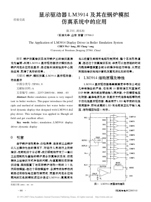
经验交流显示驱动器L M3914及其在锅炉模拟仿真系统中的应用陈卫红,胡长松(石油大学,山东东营257061)The Application of L M3914Display Driver in Boiler Emulation SystemCHEN Wei hong ,HU Chang song(University of Petroleum ,Dongying 257061,China ) 摘要:锅炉仿真培训系统对锅炉工的培训显得尤为重要。
利用LM3914显示驱动器设计模拟热水锅炉汽包水位动态显示,通过胜利油田检测中心现场应用,取得了良好的效果。
关键词:锅炉;模拟仿真;LM3914显示驱动器;动态显示中图分类号:TP391.9文献标识码:A文章编号:1001-2257(2003)04-0068-03Abstract :Boiler emulation system is very impor 2tant to boiler workers.This paper introduces the prin 2ciple and method of simulative hot water boiler water level dynamic display that designed with LM3914dis 2play driver.This technique was applied in Shengli oil field and got excellent effect.K ey w ords :boiler ;simulation ;LM3914display driver ;dynamic display收稿日期:2002-09-030 引言由于锅炉结构复杂、价格昂贵,在目前工业锅炉以人工操作为主的情况下,对运行人员进行上岗前培训、定期轮训十分必要。
我们研制和开发了一套以工业控制机为基础的锅炉混合仿真培训系统,彻底解决上述培训方式存在的问题。