2SC1815O中文资料
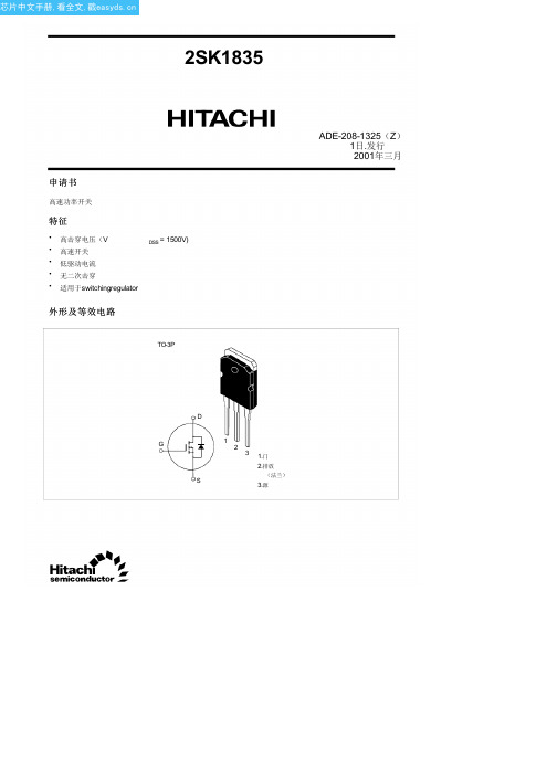
2SK1835中文资料(hitachi)中文数据手册「EasyDatasheet - 矽搜」
50
100
150
200
Case Temperature Tc (°C)
最大安全作业区 50 30
10
10
(A)
10 0
µs
D
3
DCOpePW=
1ms 10
µs
Drain Cu1rrent I
ration(Tcm=s2(15shot)
0.3 Operation in this
°C )
area isilmited by
静态漏极至源关于国家 电阻与漏极电流
50
20
Ω) (on) ( 10
Pulse Test
DS
5 Resistance R
Static Drain2–Source on State
VGS = 10 V 15 V
1
0.5
20
0.2
0.5 1 2
5 10 20
Drain Current I D (A)
静态漏极至源关于国家 电阻与温度
符
V DSS V GSS ID I *1
D(puls e)
IDR Pch* 2 Tch Tstg
评级
Unit
1500
V
±20
V
4
10
A
4
A
125
W
150
°C
-55到+150
°C
2
芯片中文手册,看全文,戳
电气特性
Item
漏源击穿 电压 门源漏电流
零栅压漏电流I
门源截止电压 静态漏极至源极导通状态 抵抗性 远期转移导纳
25
远期转移导纳 主场迎战漏电流
10
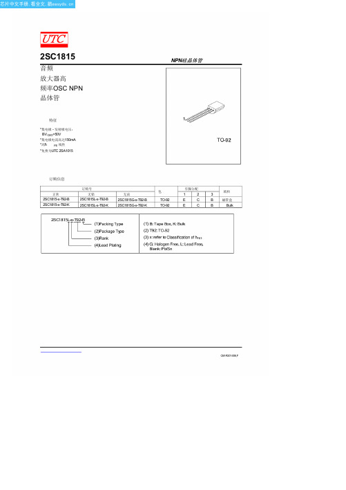
2SC1815中文资料(Unisonic Technologies)中文数据手册「EasyDatasheet - 矽搜」
电气特性
(TA = 25℃,除非另有规定)
参数 集电极截止电流 发射极截止电流
集电极 - 发射极饱和电压
基地发射极饱和电压
DC电流增益
当前增益带宽产品 输出电容
噪声系数
^ h分类
符号
I CBO IEBO VCE(SAT) VBE(SAT) hFE1 hFE2 fT Cob
NF
测试条件
VCB=60V, I E=0 VEB=5V, I C=0 IC=100mA, I B=10mA IC=100mA, I B=10mA VCE=6V, I C=2mA VCE=6V, I C=150mA VCE=10V, I C=50mA VCB=10V, I E=0, f=1MHz IC=-0.1mA, V CE=6V RG=10kΩ, f=100Hz
NPN硅晶体管
绝对最大额定值
(TA = 25℃,除非另有规定)
参数
符号
集电极基极电压
VCBO
集电极 - 发射极电压
VCEO
发射极基极电压
V EBO
集电极电流
IC
基极电流
IB
功耗(TA = 25℃)
PD
结温
TJ
储存温度
TSTG
注意绝对最大额定值是那些超出该装置可以永久损坏值.
绝对最大额定值是压力额定值只和功能设备操作不暗示.
QW-R201-006,F
芯片中文手册,看全文,戳
2SC1815
典型特征
NPN硅晶体管
QW-R201-006,F
芯片中文手册,看全文,戳
2SC1815
NPN硅晶体管
UTC不承担由于使用产品超过,即使是瞬间值,设备故障不承担任何责任,额定数值(例如最大额 定值,工作环境范围或其他参数)任何产品规格和描述或此处包含所有UTC产品上市. UTC产 品并非设计用于生命支持设备,装置或在这些产品故障可合理预期会导致人身伤害系统.严禁复制 全部或部分未经版权拥有者事先书面同意.本文件中不构成任何报价或合同一部分信息,被认为 是准确可靠,恕不另行通知可随时更改.
2SC1815中文资料
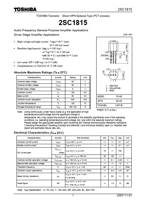
TOSHIBA Transistor Silicon NPN Epitaxial Type (PCT process)2SC1815Audio Frequency General Purpose Amplifier ApplicationsDriver Stage Amplifier Applications•High voltage and high current: V CEO = 50 V (min),I C = 150 mA (max)•Excellent h FE linearity : h FE (2) = 100 (typ.)atV CE = 6 V, I C = 150 mA:h FE (I C = 0.1 mA)/h FE (I C = 2 mA)= 0.95 (typ.)•Low noise: NF = 1dB (typ.) at f = 1 kHz•Complementary to 2SA1015 (O, Y, GR class)Absolute Maximum Ratings (Ta = 25°C)Characteristics SymbolRatingUnitCollector-base voltage V CBO 60 VCollector-emitter voltage V CEO 50 VEmitter-base voltage V EBO 5 VCollector current I C 150mABase current I B 50mACollector power dissipation P C 400mWJunction temperature T j125 °CStorage temperature range T stg−55~125 °CNote: Using continuously under heavy loads (e.g. the application of hightemperature/current/voltage and the significant change intemperature, etc.) may cause this product to decrease in the reliability significantly even if the operatingconditions (i.e. operating temperature/current/voltage, etc.) are within the absolute maximum ratings.Please design the appropriate reliability upon reviewing the Toshiba Semiconductor Reliability Handbook(“Handling Precautions”/“Derating Concept and Methods”) and individual reliability data (i.e. reliability testreport and estimated failure rate, etc).Electrical Characteristics (Ta = 25°C)Characteristics Symbol TestCondition MinTyp.Max Unit Collector cut-off current I CBO V CB= 60 V, I E= 0 ⎯ ⎯ 0.1 μA Emitter cut-off current I EBO V EB= 5 V, I C= 0 ⎯⎯ 0.1 μAh FE (1)(Note)V CE= 6 V, I C= 2 mA 70 ⎯ 700DC current gainh FE (2)V CE= 6 V, I C= 150 mA 25 100 ⎯Collector-emitter saturation voltage V CE (sat)I C= 100 mA, I B= 10 mA ⎯ 0.1 0.25V Base-emitter saturation voltage V BE (sat)I C= 100 mA, I B= 10 mA ⎯⎯ 1.0 V Transition frequency f T V CE= 10 V, I C= 1 mA 80 ⎯⎯ MHz Collector output capacitance C ob V CB= 10 V, I E= 0, f = 1 MHz ⎯ 2.0 3.5 pFBase intrinsic resistance r bb’V CE= 10 V, I E=−1 mAf = 30 MHz⎯ 50 ⎯ΩNoise figure NF V CE= 6 V, I C= 0.1 mAf = 1 kHz, R G= 10 kΩ⎯ 1.0 10 dBNote: h FE classification O: 70~140, Y: 120~240, GR: 200~400, BL: 350~700Unit: mmJEDEC TO-92 JEITA SC-43 TOSHIBA 2-5F1B Weight: 0.21 g (typ.)RESTRICTIONS ON PRODUCT USE20070701-EN GENERAL •The information contained herein is subject to change without notice.•TOSHIBA is continually working to improve the quality and reliability of its products. Nevertheless, semiconductor devices in general can malfunction or fail due to their inherent electrical sensitivity and vulnerability to physical stress. It is the responsibility of the buyer, when utilizing TOSHIBA products, to comply with the standards of safety in making a safe design for the entire system, and to avoid situations in which a malfunction or failure of such TOSHIBA products could cause loss of human life, bodily injury or damage to property.In developing your designs, please ensure that TOSHIBA products are used within specified operating ranges as set forth in the most recent TOSHIBA products specifications. Also, please keep in mind the precautions and conditions set forth in the “Handling Guide for Semiconductor Devices,” or “TOSHIBA Semiconductor Reliability Handbook” etc.• The TOSHIBA products listed in this document are intended for usage in general electronics applications (computer, personal equipment, office equipment, measuring equipment, industrial robotics, domestic appliances, etc.).These TOSHIBA products are neither intended nor warranted for usage in equipment that requires extraordinarily high quality and/or reliability or a malfunction or failure of which may cause loss of human life or bodily injury (“Unintended Usage”). Unintended Usage include atomic energy control instruments, airplane or spaceship instruments, transportation instruments, traffic signal instruments, combustion control instruments, medical instruments, all types of safety devices, etc.. Unintended Usage of TOSHIBA products listed in his document shall be made at the customer’s own risk.•The products described in this document shall not be used or embedded to any downstream products of which manufacture, use and/or sale are prohibited under any applicable laws and regulations.• The information contained herein is presented only as a guide for the applications of our products. No responsibility is assumed by TOSHIBA for any infringements of patents or other rights of the third parties which may result from its use. No license is granted by implication or otherwise under any patents or other rights of TOSHIBA or the third parties.• Please contact your sales representative for product-by-product details in this document regarding RoHS compatibility. Please use these products in this document in compliance with all applicable laws and regulations that regulate the inclusion or use of controlled substances. Toshiba assumes no liability for damage or losses occurring as a result of noncompliance with applicable laws and regulations.。
C1815中文资料参数

-
-
fT
Current Gain Ban dwidth Product
电流增益带宽
VCE=10V, IC=1mA
80
-
Cob
Output Capacitanee输出电容
VCB=10V, IE=0, f=1MHz
-
NF
Noise Figure噪声系数
VCE=6V, IC= RS=10kQ, f=1Hz
C1815中文资料参数-2SC1815引脚图-三极管C1815管脚排列-代换
本译文译自FAIRCHILE公司 东芝 飞利浦的1815特性与之基本相同
1TO-92
1发射极2.集电极3.基极
C1815三极管排列引脚图
命名:2SC1815如果叫法省略通常的叫法C18151815
2SC1815代换型号:2SC945管脚排列一是样的
-
单
放大倍数表示:
后缀符号
O
Y
GR
放大倍数
70-140
120-240
200-400
350-700
静态特性曲线
J-J
1
Q.1
0.0
0.60 8
IO1 2
10
Ve4Vl?BASE-EMITTER VOLTAGE
传输特性曲线
1
10
100
o
4—
N-volNUJMHnoacJ也匸
woo
直流电流增益曲线
[c[mAl.COLLECTOR CURRENT
150
主要参数:
U
IB
Base Current基极电流
50
mA
PC
Collector Power Dissipation耗散功率
2sc1815主要参数
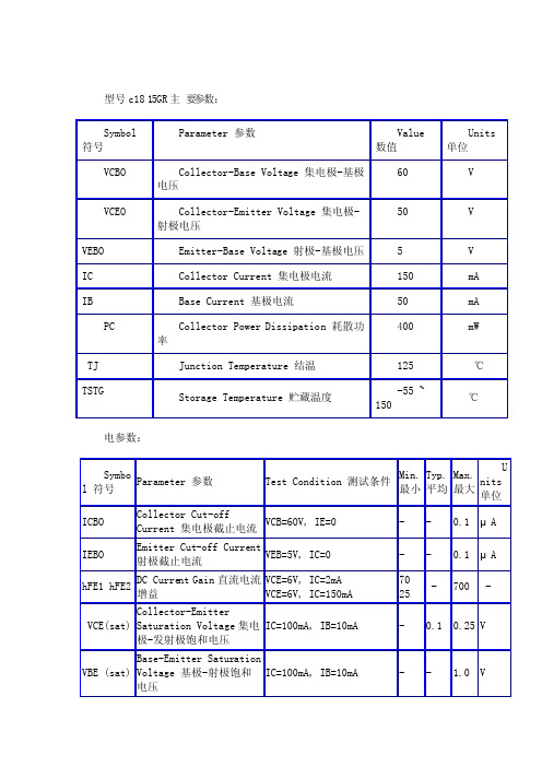
型号c1815GR主要参数:电参数:9013主要参数1815三极管参数集电极-基极击穿电压(VCBO):60V集电极-发射极击穿电压(VCEO):50V 发射极-基极击穿电压(VEBO):5V集电极电流(IC):150mA基极电流(IB):50mA耗散功率(PC):400mW集电极-发射极饱和压降(VCE):0.25V 特征频率(fr):80MHz1815三极管参数集电极-基极击穿电压(VCBO):60V集电极-发射极击穿电压(VCEO):50V发射极-基极击穿电压(VEBO):5V集电极电流(IC):150mA基极电流(IB):50mA耗散功率(PC):400mW集电极-发射极饱和压降(VCE):0.25VC9013NPN三极管集电极漏电流ICBOVCB=30V,IE=0 100 nA发射极漏电流IEBOVBE=5V,IC=0 100 nA集电极、发射极击穿电压BVCE O IC=1mA,IB=0 25 V发射极、基极击穿电压BVEBO IE=100μA,IC=0 5 V集电极、基极击穿电压BVCBO IC=100μA,IE=0 30 V集电极、发射极饱和压降VCE(sat)IC=500mA,IB=50mA 0.6 V基极、发射极饱和压降VBE(sat)IC=500mA,IB=50mA 1.2 V基极、发射极压降V BE VCE=1V,IC=10mA 1.0 V直流电流增益HFE1VCE=1V,IC=50mA 96 300HFE2 VCE=1V,IC=500mA401.2参数符号标称值单位集电极、基极击穿电压VCBO30 V集电极、发射极击穿电压VCEO 25 V发射极、基极击穿电压VEBO5 V集电极电流I C 500 mA集电极功率P C 625 mW结温TJ 150 ℃贮存温TST G -55-150 ℃6发射△电参数(Ta=25℃)(按HEF1分类)标准分档:F:96-135 G:112-166 H:144-202 I:200-300 TO-92F G H1 H2 I1 I296-120 120-150 150-170 170-200 200-250 250-300。
2SC1815 PDF规格书
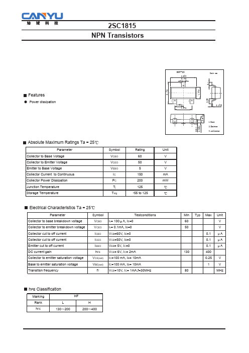
COMMON EMITTER Ta=25℃ hFE
(mA)
4
Ta=100℃ Ta=25℃
12uA
3
IC
COLLECTOR CURRENT
10uA 8uA
DC CURRENT GAIN 4uA IB=2Fra bibliotekA100
2
6uA
1
COMMON EMITTER VCE= 6V
10 10 0.1 1 10 100 150
10
200
Cib Cob
C
150
CAPACITANCE
100
50
0.1 0.1
1
10
20
0
0
25
50
75
100
125
150
REVERSE VOLTAGE
V
(V)
AMBIENT TEMPERATURE
Ta
(℃)
(mA)
IC
COLLECTOR CURRENT
10
TRANSITION FREQUENCY
T= a 10 0℃
T= a 25 ℃
fT
100 1
(MHz)
COMMON EMITTER VCE= 6V
0.1
0
BASE-EMMITER VOLTAGE VBE (mV)
300
600
900
1200
10 0.1
3
+0.05 0.1 -0.01
+0.1 0.97 -0.1
1.Base 2.Emitter 3.collector
Absolute Maximum Ratings Ta = 25
Parameter Collector to Base Voltage Collector to Emitter V oltage Emitter to Base Voltage Collector Current to Continuous Collector Power Dissipation Junction Temperature Storage Temperature Symbol VCBO VCEO VEBO IC PC Tj Tstg Ra t i n g 60 50 5 150 200 125 -55 to 125 Un i t V V V mA mW
2SC1815K中文资料
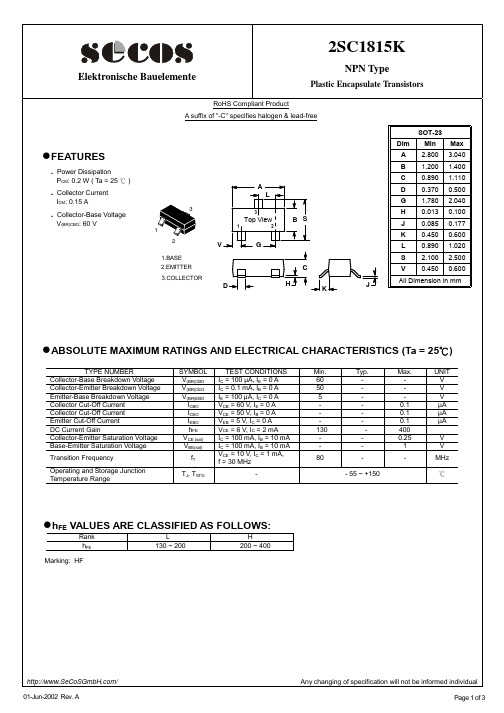
Page 2 of 3
元器件交易网
2SC1815K
Elektronische Bauelemente NPN Type
Plastic Encapsulate Transistors
/
01-Jun-2002 Rev. A
Any changing of specification will not be informed in.800 1.200 0.890 0.370 1.780 0.013 0.085 0.450 0.890 2.100 0.450 Max 3.040 1.400 1.110 0.500 2.040 0.100 0.177 0.600 1.020 2.500 0.600
V
G C D H K J
1.BASE 2.EMITTER 3.COLLECTOR
V
All Dimension in mm
ABSOLUTE MAXIMUM RATINGS AND ELECTRICAL CHARACTERISTICS (Ta = 25 )
TYPE NUMBER Collector-Base Breakdown Voltage Collector-Emitter Breakdown Voltage Emitter-Base Breakdown Voltage Collector Cut-Off Current Collector Cut-Off Current Emitter Cut-Off Current DC Current Gain Collector-Emitter Saturation Voltage Base-Emitter Saturation Voltage Transition Frequency Operating and Storage Junction Temperature Range SYMBOL V(BR)CBO V(BR)CEO V(BR)EBO ICBO ICEO IEBO hFE VCE (sat) VBE(sat) fT TJ, TSTG TEST CONDITIONS IC = 100 µA, IE = 0 A IC = 0.1 mA, IB = 0 A IE = 100 µA, IC = 0 A VCB = 60 V, IE = 0 A VCE = 50 V, IB = 0 A VEB = 5 V, IC = 0 A VCE = 6 V, IC = 2 mA IC = 100 mA, IB = 10 mA IC = 100 mA, IB = 10 mA VCE = 10 V, IC = 1 mA, f = 30 MHz Min. 60 50 5 130 80 Typ. - 55 ~ +150 Max. 0.1 0.1 0.1 400 0.25 1 UNIT V V V µA µA µA V V MHz
C1815中文资料参数
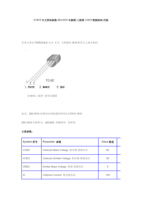
C1815中文资料参数-2Sc1815引脚图-三极管c1815管脚排列-代换
本译文译自FAIRCHILE公司东芝飞利浦的1815特性与之基本相同
C1815三极管排列引脚图
命名:2SC1815如果叫法省略通常的叫法C1815 1815
2SC1815代换型号:2SC945 管脚排列一是样的
主要参数:
Symbol符号Parameter 参数Value数值Un VCBO Collector-Base Voltage 集电极-基极电压60
VCEO Collector-Emitter Voltage 集电极-射极电压50
VEBO Emitter-Base Voltage 射极-基极电压 5
IC Collector Current 集电极电流150
电参数:
放大倍数表示:
后缀符号O Y GR L 放大倍数70-140120-240200-400350-700
C1815特性曲线:
静态特性曲线
传输特性曲线
直流电流增益曲线
基极-发射饱和电压曲线集电极-射极饱和电压曲线
输出电容曲线
电流增益带宽曲线
外形封装图。
c2sc1815放大器

这个电路是一个最简单的放大器,算是一个古董电路!下面将对这个电路进行直流分析:电路组成:三极管是电路的放大元件,具有放大电流的作用,是放大电路的“心脏”;电源V CC的接法应使集电极处于反向偏置,保证晶体管工作在放大状态,同时V CC 为放大电路提供能源,一般为几伏到几十伏。
很多电路中一般是用电压来传递信号,如果在三极管集电极与电源之间串一个电阻,这样能把三极管的电流信号转换为电压信号取出来。
集电极负载电阻R2的主要作用是将集电极电流的变化转换为电压的变化,以实现电压的放大。
R2的阻值一般为几千欧。
负载电阻越大,得到的电压信号变化也会越大。
电源V CC和基极电阻R1的作用是使发射结处于正向偏置,并提供大小适当的基极电流I B,以便放大电路获得合适的工作点。
R1的阻值一般为几十千欧到几百千欧。
耦合电容C1的作用在于隔断直流、通过交流。
因此,它既能为交流信号构成通路,同时又能隔断放大电路、信号源及负载之间的直流通路,使信号源及负载的工作状态免收直流电源的影响。
通常要求C1上的交流电压可以降到可以忽略不计,即对交流信号可视为短路。
C1的电容值一般为几微法到几十微法,常用极性电容,连接时应注意极性。
如果把I C的变化作为输出而取出,就可以得到比较大的信号。
直流工作概念:直流工作的时候,电容上没有流过电流,所以在直流分析中都会将所有的电容看成开路。
这个是原理图,在做直流分析的时候,交流信号源和电容C1都看成开路。
设计一个电路的时候,要先确定I C也就是集电极电流。
V CC=V CE+R2*I C电源电压=三极管CE极电压+负载电阻×集电极电流先定V CE=6V 集电极电阻为10K ,除去两个变量,就好办多了。
12=6+10000* I CI C=(12-6)/10000I C=0.6mA有了I C就可以确定I B了。
I B=I C/放大倍数(放大倍数现定为100)I B=0.6/100;I B=6uA.I B确定后,可以确定 R1也就是为三极管基极提供电流的电阻。
2SC1580资料
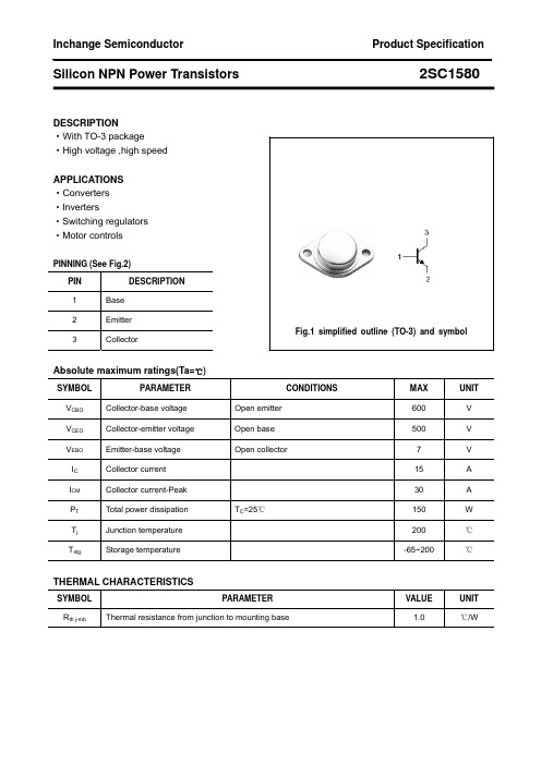
Inchange Semiconductor Product Specification
Silicon NPN Power Transistors
2SC1580
DESCRIPTION ·With TO-3 package ·High voltage ,high speed APPLICATIONS ·Converters ·Inverters ·Switching regulators ·Motor controls
2SC1580
TYP.
MAX
UNIT V V
1.5 2.0 0.1 0.1 25 5
V V mA mA
MHz
2
元器件交易网
Inchange Semiconductor Product Specification
Silicon NPN Power Transistors
PACKAGE OUTLINE
2SC1580
Fig.2 Outline dimensions
3
Hale Waihona Puke Silicon NPN Power Transistors
CHARACTERISTICS
Tj=25℃ unless otherwise specified SYMBOL V(BR)CEO V(BR)EBO VCEsat VBEsat ICBO IEBO hFE fT PARAMETER Collector-emitter breakdown voltage Emitter-base breakdown voltage Collector-emitter saturation voltage Base-emitter saturation voltage Collector cut-off current Emitter cut-off current DC current gain Transition frequency CONDITIONS IC=10mA ; IB=0 IE=1mA ; IC=0 IC=10A; IB=2A IC=10A; IB=2A VCB=600V; IE=0 VEB=7V; IC=0 IC=5A ; VCE=4V IC=0.5A ; VCE=10V 10 MIN 500 7
C1815中文资料参数

C1815中文资料参数-2Sc1815引脚图-三极管c1815管脚排列-代换
本译文译自FAIRCHILE公司东芝飞利浦的1815特性与之基本相同
C1815三极管排列引脚图
命名:2SC1815如果叫法省略通常的叫法C1815 1815
2SC1815代换型号:2SC945 管脚排列一是样的
主要参数:
Symbol符号Parameter 参数Value数值Un VCBO Collector-Base Voltage 集电极-基极电压60
VCEO Collector-Emitter Voltage 集电极-射极电压50
VEBO Emitter-Base Voltage 射极-基极电压 5
IC Collector Current 集电极电流150
电参数:
放大倍数表示:
后缀符号O Y GR L 放大倍数70-140120-240200-400350-700
C1815特性曲线:
静态特性曲线
传输特性曲线
直流电流增益曲线
基极-发射饱和电压曲线集电极-射极饱和电压曲线
输出电容曲线
电流增益带宽曲线
外形封装图。
2SA1841L资料

The information in this document is subject to change without notice. Before using this document, pleaseconfirm that this is the latest version.Not all products and/or types are available in every country. Please check with an NEC Electronics sales representative for availability and additional information.DATA SHEETDocument No. D15590EJ3V0DS00 (3rd edition)Date Published July 2004 NS CP(K) Printed in Japan2002ORDERING INFORMATIONPART NUMBERPACKAGE 2SA1841MP-10DESCRIPTIONThe 2SA1841 is a high-speed Darlington power transistor. This transistor is ideal for high-precision control such as PWM control for pulse motors brushless motors in OA and FA equipment. In addition, this transistor features a package that can be auto-mounted in radial taping specifications, thus contributing to mounting cost reduction.FEATURES• Auto-mounting possible in radial taping specifications• Resin-molded insulation type package with power rating of 1.8 W in stand-alone conditions • High DC current amplifiers due to Darlington connection h FE = 4000 to 20000 (V CE = −2.0 V, I C = −4.0 A) • On-chip C-to-E reverse diode • Fast switching speedABSOLUTE MAXIMUM RATINGS (T A = 25°C)Collector to Base Voltage V CBO −100 V Collector to Emitter Voltage V CEO −100 V Emitter to Base Voltage V EBO −8.0 V Collector Current (DC) I C(DC) −8.0 A Collector Current (pulse) I C(pulse) Note −16 A Base Current (DC)I B(DC) −0.8 A Total Power Dissipation (T A = 25°C) P T 1.8 W Junction Temperature T j 150 °CStorage TemperatureT stg−55 to +150°CNote PW ≤ 10 ms, Duty Cycle ≤ 2%The mark ★ shows major revised points.★Data Sheet D15590EJ3V0DS2ELECTRICAL CHARACTERISTICS (T A = 25°C)CHARACTERISTICS SYMBOL TEST CONDITIONS MIN. TYP. MAX. UNITCollector Cut-off Current I CBO V CB = −100 V, I E = 0 A −1.0 µ AEmitter Cut-off Current I EBO V EB = −5.0 V, I C = 0 A −5.0 mA DC Current Gain Noteh FE1 V CE = −2.0 V, I C = −4.0 A 4000 20000h FE2V CE = −2.0 V, I C = −8.0 A 500Collector Saturation Voltage NoteV CE(sat) I C = −4.0 A, I B = −4.0 mA −1.5 V Base Saturation Voltage NoteV BE(sat) I C = −4.0 A, I B = −4.0 mA −2.0 V Turn-on Time t on I C = −4.0 A 0.2 µs Storage Time t stg I B1 = −I B2 = −4.0 mA 1.5 µs Fall Timet fR L = 12.5 Ω, V CC = −50 V0.7µsNote Pulsed test PW ≤ 350 ms, Duty Cycle ≤ 2%h FE CLASSIFICATIONMarking L Kh FE14000 to 100008000 to 20000SWITCHING TIME (t on , t stg , t f ) TEST CIRCUITV CCR LI B1I B2I CI CT.U.T.V INPWPW = 50 sV BB = −5 VDuty Cycle ≤ 2%Base currentwaveform Collector current waveformt ont stg t f90%I B1I B210%....µ★Data Sheet D15590EJ3V0DS3TYPICAL CHARACTERISTICS (T A = 25°C)T o t a l P o w e r D i s s i p a t i o n P T (W )Ambient Temperature Ta (°C)Pulse testD C C u r r e n t G a i n h F ECollector to Emitter Voltage V CE (V)Ambient Temperature Ta (°C)I C D e r a t i n g d T (%)C o l l e c t o r C u r r e n t I C (A )C o l l e c t o r C u r r e n t I C (A )T r a n s i e n t T h e r m a l R e s i s t a n c e r t h (j -a )(t ) (°C /W )Pulse Width PW (s)Collector to Emitter Voltage V CE (V)Collector Current I C (A)Single pulseData Sheet D15590EJ3V0DS4Collector Current I C (A)Collector Current I C (A)Collector Current I C (A)Pulse testPulse testC o l l e c t o r S a t u r a t i o n V o l t a g e V C E (s a t ) (V )B a s e S a t u r a t i o n V o l t a g e V B E (s a t ) (V )G a i n B a n d w i d t h P r o d u c t f T (M H z )C o l l e c t o r C a p a c i t a n c e C o b (p F )Collector to Base Voltage V CB (V)Data Sheet D15590EJ3V0DS5PACKAGE DRAWING (Unit: mm)TAPING SPECIFICATIONH 1l 1H 1A 1P 2P 0D 0PT A 1A D 0d F 1F 2H H 0H 1 h l 1P P 0P 2 P T W W 0W 1W 28.0 ± 0.213.0 ± 0.2 4.0 ± 0.20.5 ± 0.12.5 2.5 20.0 MAX.16.0 ± 0.532.2 MAX.0 ± 1.02.5 MIN.12.7 ± 1.012.7 ± 0.36.35 ± 0.50 ± 1.34.5 ± 0.218.0 5.0 MIN.9.0 ± 0.50.7 MIN.h ∆P∆h∆∆φ∆H 1AW 2W 0W 1WdF 1F 2+0.4−0.1+0.4−0.1+1.0−0.5EQUIVALENT CIRCUIT1R 1.R 2 = 300 Ω..1. Base2. Collector3. Emitter★The information in this document is current as of July, 2004. The information is subject to change without notice. For actual design-in, refer to the latest publications of NEC Electronics data sheets or data books, etc., for the most up-to-date specifications of NEC Electronics products. Not all products and/or types are available in every country. Please check with an NEC Electronics sales representative for availability and additional information.No part of this document may be copied or reproduced in any form or by any means without the prior written consent of NEC Electronics. NEC Electronics assumes no responsibility for any errors that may appear in this document.NEC Electronics does not assume any liability for infringement of patents, copyrights or other intellectual property rights of third parties by or arising from the use of NEC Electronics products listed in this document or any other liability arising from the use of such products. No license, express, implied or otherwise, is granted under any patents, copyrights or other intellectual property rights of NEC Electronics or others.Descriptions of circuits, software and other related information in this document are provided for illustrative purposes in semiconductor product operation and application examples. The incorporation of these circuits, software and information in the design of a customer's equipment shall be done under the full responsibility of the customer. NEC Electronics assumes no responsibility for any losses incurred by customers or third parties arising from the use of these circuits, software and information.While NEC Electronics endeavors to enhance the quality, reliability and safety of NEC Electronics products, customers agree and acknowledge that the possibility of defects thereof cannot be eliminated entirely. To minimize risks of damage to property or injury (including death) to persons arising from defects in NEC Electronics products, customers must incorporate sufficient safety measures in their design, such as redundancy, fire-containment and anti-failure features.NEC Electronics products are classified into the following three quality grades: "Standard", "Special" and "Specific".The "Specific" quality grade applies only to NEC Electronics products developed based on a customer-designated "quality assurance program" for a specific application. The recommended applications of an NEC Electronics product depend on its quality grade, as indicated below. Customers must check the quality grade of each NEC Electronics product before using it in a particular application.The quality grade of NEC Electronics products is "Standard" unless otherwise expressly specified in NEC Electronics data sheets or data books, etc. If customers wish to use NEC Electronics products in applications not intended by NEC Electronics, they must contact an NEC Electronics sales representative in advance to determine NEC Electronics' willingness to support a given application.(Note)••••••M8E 02. 11-1(1)(2)"NEC Electronics" as used in this statement means NEC Electronics Corporation and also includes itsmajority-owned subsidiaries."NEC Electronics products" means any product developed or manufactured by or for NEC Electronics (asdefined above).Computers, office equipment, communications equipment, test and measurement equipment, audioand visual equipment, home electronic appliances, machine tools, personal electronic equipment and industrial robots.Transportation equipment (automobiles, trains, ships, etc.), traffic control systems, anti-disastersystems, anti-crime systems, safety equipment and medical equipment (not specifically designed for life support).Aircraft, aerospace equipment, submersible repeaters, nuclear reactor control systems, lifesupport systems and medical equipment for life support, etc."Standard":"Special":"Specific":。
C中文资料参数

C1815中文资料参数-2Sc1815引脚图-三极管c1815管脚排列-代换
本译文译自FAIRCHILE公司东芝飞利浦的1815特性与之基本相同
C1815三极管排列引脚图
命名:2SC1815如果叫法省略通常的叫法C1815 1815
2SC1815代换型号:2SC945 管脚排列一是样的
主要参数:
Symbol符号Parameter 参数Value数值Un VCBO Collector-Base Voltage 集电极-基极电压60
VCEO Collector-Emitter Voltage 集电极-射极电压50
VEBO Emitter-Base Voltage 射极-基极电压 5
IC Collector Current 集电极电流150
电参数:
放大倍数表示:
后缀符号O Y GR L 放大倍数70-140120-240200-400350-700
C1815特性曲线:
静态特性曲线
传输特性曲线
直流电流增益曲线
基极-发射饱和电压曲线集电极-射极饱和电压曲线
输出电容曲线
电流增益带宽曲线
外形封装图。
- 1、下载文档前请自行甄别文档内容的完整性,平台不提供额外的编辑、内容补充、找答案等附加服务。
- 2、"仅部分预览"的文档,不可在线预览部分如存在完整性等问题,可反馈申请退款(可完整预览的文档不适用该条件!)。
- 3、如文档侵犯您的权益,请联系客服反馈,我们会尽快为您处理(人工客服工作时间:9:00-18:30)。
Features
• 2SC1815 is NPN Silicon Epitaxial Transistor Designed for RF, AF Amplifier and General Purpose Applications.• Capable of 0.4Watts of Power Dissipation.• Collector-current 0.15A • Collector-base Voltage 60V •
Marking : C1815
2SC1815-Y NPN Silicon Epitaxial Transistor
Electrical Characteristics @ 25O
C Unless Otherwise Specified
Symbol Parameter
Min Max Units OFF CHARACTERISTICS
V (BR)CEO Collector-Emitter Breakdown Voltage* (I C =0.1mAdc,I B =0)
50 Vdc V (BR)CBO Collector-Base Breakdown Voltage (I C =100uAdc,I E =0)60 Vdc
V BEF Emitter-Base Voltage (I E =310mAdc)
1.45
Vdc
I CBO Collector Cutoff Current (V CB =60Vdc,I E =0Adc)0.1 uAdc I CEO Collector Cutoff Current (V CB =50Vdc,I E =0Adc)0.1 uAdc I EBO
Emitter Cutoff Current (V EB =5.0Vdc,I C =0Adc)
0.1
uAdc
ON CHARACTERISTICS
h FE(1)DC Current Gain*
(I C =2.0mAdc,V CE =6.0Vdc)
70
700 V CE(sat)Collector-Emitter Saturation Voltage (I C =100mAdc,I B =10mAdc)0.25
Vdc V BE(sat) Base-Emitter Saturation Voltage (I C =100mAdc,I B =10mAdc) 1.0
Vdc SMALL-SIGNAL CHARACTERISTICS
f T
Transistor Frequency
(I C =1.0mAdc,V CE =10Vdc, f=30MHz)
80MHz CLASSIFICATION OF H FE (1)
Rank O Y GR
BL Range
70-140
120-240
200-400
350-700
V BE
Base-Emitter Voltage (I E =310mAdc)
--- 1.45
Vdc
Revision: 6 2008/02/01
omp onents 20736Marilla Street Chatsworth
! "# $ % ! "#
Micro Commercial Components
www.mccsemi .com
1 of 2
x Case Material: Molded Plastic. UL Flammability
Classification Rating 94V-0 and MSL rating 1
2SC1815-GR 2SC1815-BL
2SC1815-O • Lead Free Finish/Rohs Compliant ("P"Suffix designates
Compliant. See ordering information)
Revision: 6 2008/02/01
Micro Commercial Components
www.mccsemi .com
2 of 2
products are represented on our website, harmless against all damages.
***APPLICATIONS DISCLAIMER***
***IMPORTANT NOTICE***Aerospace or Military Applications.
Products offer by Micro Commercial Components Corp .are not intended for use in Medical,
Micro Commercial Components Corp .reserve s the right to make changes without further notice to any
product herein to make corrections, modifications , enhancements , improvements , or other changes .Micro Commercial Components Corp .does not assume any liability arising out of the application or use of any product described herein; neither does it convey any license under its patent rights ,nor the rights of others . The user of products in such applications shall assume all risks of such use and will agree to hold Micro Commercial Components Corp .and all the companies whose
Ordering Information
Device Packing
(Part Number)-AP Ammo Packing;2Kpcs/AmmoBox (Part Number)-BP Bulk;1Kpcs/Bag。
