A5842SLW中文资料
UCN5841中文资料

Output Voltage, VCE (5841) . . . . . . . . . . . . . . . . . . . . . . 50 V (5842) . . . . . . . . . . . . . . . . . . . . . . 80 V
SUB
1
POWER GROUND
9
Dwg. FP-013-2
A5841SLW & A5842SLW
POWER GROUND
1
SUB
CLOCK 2 CLK
SERIAL DATA IN
3
GROUND 4
LOGIC SUPPLY 5 VDD
SERIAL DATA OUT
6
STROBE 7 ST
OUTPUT ENABLE
5 LOGIC SUPPLY
SERIAL-PARALLEL SHIFT REGISTER
6
SERIAL DATA OUT
LATCHES
7 STROBE
8
OUTPUT ENABLE (ACTIVE LOW)
MOS
BIPOLAR
18
17
16
15
14
13
12
11
10
OUT 1 OUT 2 OUT 3 OUT 4 OUT 5 OUT 6 OUT 7 OUT 8 K
PD . . . . . . . . . . . . . . . . . . . See Graph Operating Temperature Range,
TA . . . . . . . . . . . . . . . . -20°C to +85°C Storage Temperature Range,
BZX584C2V7-02V中文资料
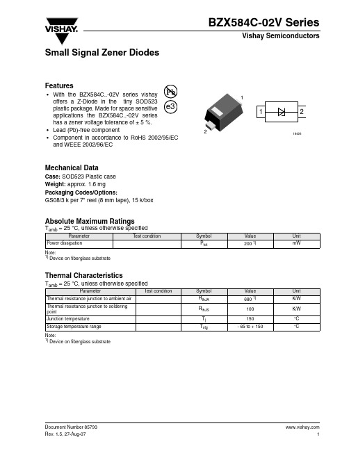
BZX584C-02V SeriesDocument Number 85793Rev. 1.5, 27-Aug-07Vishay Semiconductors1Small Signal Zener DiodesFeatures•With the BZX584C..-02V series vishay offers a Z-Diode in the tiny SOD523plastic package. Made for space sensitive applications the BZX584C..-02V series has a zener voltage tolerance of ± 5 %. •Lead (Pb)-free component•Component in accordance to RoHS 2002/95/EC and WEEE 2002/96/ECMechanical DataCase: SOD523 Plastic case Weight: approx. 1.6 mgPackaging Codes/Options:GS08/3 k per 7" reel (8 mm tape), 15 k/boxAbsolute Maximum RatingsT amb = 25°C, unless otherwise specifiedNote:1) Device on fiberglass substrateThermal CharacteristicsT amb = 25°C, unless otherwise specifiedNote:1)Device on fiberglass substrateParameterT est conditionSymbol Value Unit Power dissipationP tot200 1)mWParameterTest conditionSymbol Value Unit Thermal resistance junction to ambient air R thJA 680 1)K/W Thermal resistance junction to soldering pointR thJS 100K/W Junction temperature T j 150°C Storage temperature range T stg- 65 to + 150°C 2Document Number 85793Rev. 1.5, 27-Aug-07BZX584C-02V SeriesVishay Semiconductors Electrical CharacteristicsPartnumberMarking CodeZener Voltage Range Dynamic Resistance T est Current Temp. Coefficient of Zener Voltage T est Current Reverse Leakage Current V Z at 5 mAr zj at I ZT1r zj at I ZT2I ZT1αVZ at 5 mA I ZT2I R at V R V ΩmA10-4/°C mAµAVmin max min max BZX584C2V4-02V 2 2.2 2.670 (≤ 100)275 (≤ 600)5- 9.0- 4.01501BZX584C2V7-02V 3 2.5 2.975 (≤ 100)300 (≤ 600)5- 9.0- 4.01201BZX584C3V0-02V 42.83.280 (≤ 95)325 (≤ 600)5- 9.0- 3.01101BZX584C3V3-02V 5 3.1 3.585 (≤ 95)350 (≤ 600)5- 8.0- 3.0151BZX584C3V6-02V 63.4 3.885 (≤ 90)375 (≤ 600)5- 8.0- 3.0151BZX584C3V9-02V 7 3.74.185 (≤ 90)400 (≤ 600)5- 7.0- 3.0131BZX584C4V3-02V 84 4.680 (≤ 90)410 (≤ 600)5- 6.0- 1.0131BZX584C4V7-02V 9 4.4550 (≤ 80)425 (≤ 500)5-5.0+ 2.0132BZX584C5V1-02V 1 4.8 5.440 (≤ 60)400 (≤ 480)5- 3.0+ 4.0122BZX584C5V6-02V 0 5.2615 (≤ 40)80 (≤ 400)5- 2.0+6.0112BZX584C6V2-02V 1 5.8 6.6 6.0 (≤ 10)40 (≤ 150)5- 1.0+ 7.0134BZX584C6V8-02V 2 6.47.2 6.0 (≤ 15)30 (≤ 80)5+ 2.0+ 7.0124BZX584C7V5-02V 377.9 6.0 (≤ 15)30 (≤ 80)5+ 3.0+ 7.0115BZX584C8V2-02V T7.78.7 6.0 (≤ 15)40 (≤ 80)5+ 4.0+ 7.010.75BZX584C9V1-02V S 8.59.6 6.0 (≤ 15)40 (≤ 100)5+ 5.0+ 8.010.56BZX584C10-02V R9.410.68.0 (≤ 20)50 (≤ 150)5+ 5.0+ 8.010.27BZX584C11-02V P 10.411.610 (≤ 20)50 (≤ 150)5+ 5.0+ 9.010.18BZX584C12-02V 711.412.710 (≤ 25)50 (≤ 150)5+ 6.0+ 9.010.18BZX584C13-02V 512.414.110 (≤ 30)50 (≤ 170)5+ 7.0+ 9.010.18BZX584C15-02V 413.815.610 (≤ 30)50 (≤ 200)5+ 7.0+ 9.010.18BZX584C16-02V 15.317.110 (≤ 40)50 (≤ 200)5+ 8.0+ 9.510.050.7 V Znom BZX584C18-02V 16.819.110 (≤ 45)50 (≤ 225)5+ 8.0+ 9.510.050.7 V Znom BZX584C20-02V 18.821.215 (≤ 55)60 (≤ 225)5+ 8.0+ 1010.050.7 V Znom BZX584C22-02V 20.823.320 (≤ 55)60 (≤ 250)5+ 8.0+ 1010.050.7 V Znom BZX584C24-02V 22.825.625 (≤ 70)60 (≤ 250)5+ 8.0+ 1010.050.7 V Znom BZX584C27-02V 25.128.925 (≤ 80)65 (≤ 300)2+ 8.0+ 100.50.050.7 V Znom BZX584C30-02V K283230 (≤ 80)70 (≤ 300)2+ 8.0+ 100.50.050.7 V Znom BZX584C33-02V 313535 (≤ 80)75 (≤ 325)2+ 8.0+ 100.50.050.7 V Znom BZX584C36-02V 343835 (≤ 90)80 (≤ 350)2+ 8.0+ 100.50.050.7 V Znom BZX584C39-02V 374140 (≤ 130)80 (≤ 350)2+ 10+ 120.50.050.7 V Znom BZX584C43-02V 404645 (≤ 150)85 (≤ 375)2+ 10+ 120.50.050.7 V Znom BZX584C47-02V L 445050 (≤ 170)85 (≤ 375)2+ 10+ 120.50.050.7 V Znom BZX584C51-02VM485460 (≤ 180)85 (≤ 400)2+ 10+ 120.50.050.7 V Znom1241579P R1BZX584C-02V SeriesDocument Number 85793Rev. 1.5, 27-Aug-07Vishay Semiconductors3Package Dimensions in millimeters (inches): SOD523 4Document Number 85793Rev. 1.5, 27-Aug-07BZX584C-02V SeriesVishay SemiconductorsOzone Depleting Substances Policy StatementIt is the policy of Vishay Semiconductor GmbH to1.Meet all present and future national and international statutory requirements.2.Regularly and continuously improve the performance of our products, processes, distribution and operatingsystems with respect to their impact on the health and safety of our employees and the public, as well as their impact on the environment.It is particular concern to control or eliminate releases of those substances into the atmosphere which are known as ozone depleting substances (ODSs).The Montreal Protocol (1987) and its London Amendments (1990) intend to severely restrict the use of ODSs and forbid their use within the next ten years. Various national and international initiatives are pressing for an earlier ban on these substances.Vishay Semiconductor GmbH has been able to use its policy of continuous improvements to eliminate the use of ODSs listed in the following documents.1.Annex A, B and list of transitional substances of the Montreal Protocol and the London Amendmentsrespectively2.Class I and II ozone depleting substances in the Clean Air Act Amendments of 1990 by the EnvironmentalProtection Agency (EPA) in the USA3.Council Decision 88/540/EEC and 91/690/EEC Annex A, B and C (transitional substances) respectively. Vishay Semiconductor GmbH can certify that our semiconductors are not manufactured with ozone depleting substances and do not contain such substances.We reserve the right to make changes to improve technical designand may do so without further notice.Parameters can vary in different applications. All operating parameters must be validated for each customer application by the customer. Should the buyer use Vishay Semiconductors products for any unintended or unauthorized application, the buyer shall indemnify Vishay Semiconductors against all claims, costs, damages, and expenses, arising out of, directly or indirectly, any claim of personal damage, injury or death associatedwith such unintended or unauthorized use.Vishay Semiconductor GmbH, P.O.B. 3535, D-74025 Heilbronn, GermanyDocument Number: 91000Revision: 18-Jul-081DisclaimerLegal Disclaimer NoticeVishayAll product specifications and data are subject to change without notice.Vishay Intertechnology, Inc., its affiliates, agents, and employees, and all persons acting on its or their behalf (collectively, “Vishay”), disclaim any and all liability for any errors, inaccuracies or incompleteness contained herein or in any other disclosure relating to any product.Vishay disclaims any and all liability arising out of the use or application of any product described herein or of any information provided herein to the maximum extent permitted by law. The product specifications do not expand or otherwise modify Vishay’s terms and conditions of purchase, including but not limited to the warranty expressed therein, which apply to these products.No license, express or implied, by estoppel or otherwise, to any intellectual property rights is granted by this document or by any conduct of Vishay.The products shown herein are not designed for use in medical, life-saving, or life-sustaining applications unless otherwise expressly indicated. Customers using or selling Vishay products not expressly indicated for use in such applications do so entirely at their own risk and agree to fully indemnify Vishay for any damages arising or resulting from such use or sale. Please contact authorized Vishay personnel to obtain written terms and conditions regarding products designed for such applications.Product names and markings noted herein may be trademarks of their respective owners.元器件交易网。
5841中文资料

I To 3.3 MHz Data-Input Rate
I CMOS, NMOS, TTL Compatible Inputs
I Internal Pull-Up/Pull-Down Resistors
I Low-Power CMOS Logic and Latches,
I High-Voltage Current-Sink Outputs
5 LOGIC SUPPLY
SERIAL-PARALLEL SHIFT REGISTER
6
SERIAL DATA OUT
LATCHES
7 STROBE
8
OUTPUT ENABLE (ACTIVE LOW)
MOS
BIPOLAR
18
17
16
15
14
13
12
11
10
OUT 1 OUT 2 OUT 3 OUT 4 OUT 5 OUT 6 OUT 7 OUT 8 K
TS . . . . . . . . . . . . . . . -55°C to +150°C
†For inductive load applications.
Caution: CMOS devices have input static protection but are susceptible to damage when exposed to extremely high static electrical charges.
SUB
1
POWER GROUND
9
Dwg. FP-013-2
A5841SLW & A5842SLW
POWER GROUND
导电胶584-29中文说明书
导电胶584-29中文说明书摘要:一、导电胶584-29 概述二、导电胶584-29 的用途和性能三、导电胶584-29 的施工方法四、导电胶584-29 的注意事项五、结语正文:【导电胶584-29 概述】导电胶584-29 是一种双组份导电粘合剂,具有优良的导电性能和粘接性能。
它主要由导电粒子、树脂、溶剂和添加剂组成,可通过混合和涂抹的方式施工。
导电胶584-29 广泛应用于电子、电气、通信等行业,可粘接各种导电材料,如金属、石墨、碳纤维等。
【导电胶584-29 的用途和性能】导电胶584-29 的主要用途是粘接和连接各种导电材料,以实现导电通路。
其优良的导电性能和粘接性能可确保粘接后的导电材料具有稳定的导电性能,从而满足电子、电气产品的性能要求。
此外,导电胶584-29 还具有良好的耐热性、耐腐蚀性和抗氧化性,可保证在恶劣环境下仍具有稳定的性能。
【导电胶584-29 的施工方法】导电胶584-29 的施工方法如下:1.将导电胶584-29 的A、B 两组份按照规定的比例混合均匀。
2.将混合好的导电胶584-29 涂抹在待粘接的导电材料表面,并施加适当的压力,使导电胶584-29 充分渗透到粘接部位。
3.将粘接好的导电材料放置在合适的环境中,等待导电胶584-29 固化。
【导电胶584-29 的注意事项】在使用导电胶584-29 时,应注意以下几点:1.导电胶584-29 应存放在阴凉、干燥、通风的环境中,避免阳光直射和高温。
2.导电胶584-29 在施工过程中应避免与皮肤直接接触,如有接触,应立即用清水冲洗。
3.导电胶584-29 在施工过程中应避免吸入粉尘,操作时应佩戴口罩。
4.导电胶584-29 在固化过程中会释放一定的热量,应避免触摸已固化的导电胶584-29。
【结语】导电胶584-29 是一种性能优良的导电粘合剂,广泛应用于电子、电气、通信等行业。
SG5842
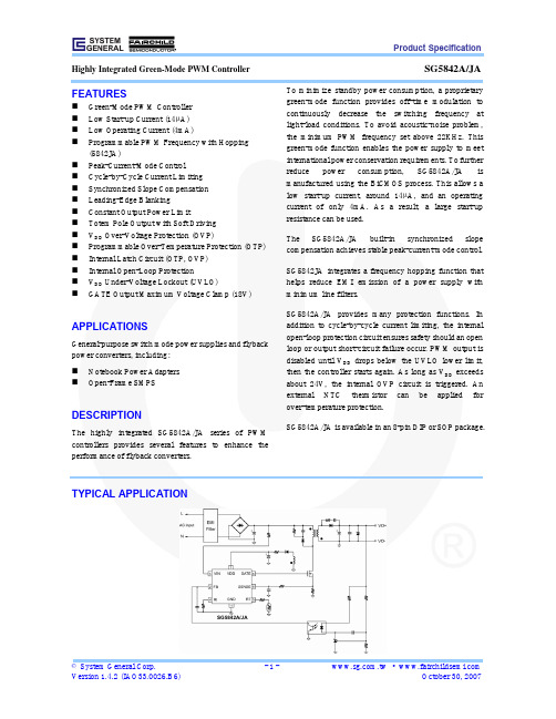
Product Specification
SG5842A/JA PIN CONFIGURATION
GND FB VIN RI
GATE VDD SENSE RT
6
SENSE
Current Sense
Current sense. The sensed voltage is used for peak-current-mode control and cycle-by-cycle current limiting.
7
VDD
Power Supply Power supply. The internal protection circuit disables PWM output if VDD is over-voltage.
ORDERING INFORMATION
Part Number
OTP Latch OVP Latch Frequency Hopping Pb-Free
SG5842JASZ
Yes
Yes
Yes
SG5842JADZ
Yes
Yes
Yes
SG5842ASZ (Preliminary) Yes
Yes
No
SG5842ADZ (Preliminary Yes
Highly Integrated Green-Mode PWM Controller
FEATURES
Green-Mode PWM Controller Low Start-up Current (14µA) Low Operating Current (4mA) Programmable PWM Frequency with Hopping
SG5841中文资料
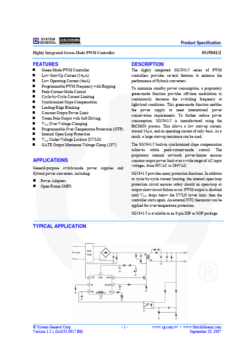
8
GATE
Driver Output The totem-pole output driver for the power MOSFET, which is internally clamped below 18V.
© System General Corp. Version 1.3.1 (IAO33.0017.B6)
SG5841/J provides many protection functions. In addition to cycle-by-cycle current limiting, the internal open-loop protection circuit ensures safety should an open-loop or output-short-circuit failure occur. PWM output is disabled until VDD drops below the UVLO lower limit, then the controller starts again. An external NTC thermistor can be applied for over-temperature protection.
T: D = DIP, S = SOP P: Z = Lead Free
Null=regular package XXXXXXXX: Wafer Lot Y: Year; WW: Week V: Assembly Location
Product Specification
SG5841/J PIN CONFIGURATION
To minimize standby power consumption, a proprietary green-mode function provides off-time modulation to continuously decrease the switching frequency at light-load conditions. This green-mode function enables the power supply to meet international power conservation requirements. To further reduce power consumption, SG5841/J is manufactured using the BiCMOS process. This allows a low start-up current, around 14µA, and an operating current of only 4mA. As a result, a large start-up resistance can be used.
MIC5841YWM TR;MIC5841YWM;MIC5841YN;MIC5841YV;MIC5842YN;中文规格书,Datasheet资料

MIC5841/58428-Bit Serial-Input Latched DriversMicrel Inc. • 2180 Fortune Drive • San Jose, CA 95131 • USA • tel +1 (408) 944-0800 • fax + 1 (408) 474-1000 • General DescriptionUsing BiCMOS technology, the MIC5841/5842 integrated circuits were fabricated to be used in a wide variety of peripheral power driver applications. The devices each have an eight-bit CMOS shift register, CMOS control circuitry, eight CMOS data latches, and eight bipolar current-sink Darlington output drivers.These two devices differ only in maximum voltage ratings. The MIC5842 offers premium performance with a minimum output breakdown voltage rating of 80V (50Vsustaining). The drivers can be operated with a split supplywhere the negative supply is down to –20V.The 500mA outputs, with integral transient-suppressiondiodes, are suitable for use with lamps, relays, solenoids and other inductive loads.These devices have improved speed characteristics. With a 5V logic supply, they will typically operate faster than 5 MHz. With a 12V supply, significantly higher speeds are obtained. The CMOS inputs are compatible with standard CMOS, PMOS, and NMOS logic levels. TTL or DTL circuits may require the use of appropriate pull-up resistors. By using the serial data output, the drivers can be cascaded for interface applications requiring additional drive lines.The MIC5840 family is available in DIP, PLCC, and SOIC packages. Because of limitations on package power dissipation, the simultaneous operation of all drivers at maximum rated current might require a reduction in duty cycle. A copper-alloy lead frame provides for maximum package power dissipation.Features• 3.3 MHz Minimum Data-Input Rate • CMOS, PMOS, NMOS, TTL Compatible• Internal Pull-Up/Pull-Down Resistors • Low-Power CMOS Logic and Latches• High-Voltage Current-Sink Outputs• Output Transient-Protection Diodes • Single or Split Supply OperationOrdering InformationPart NumberStandard Pb-Free Temperature RangePackage MIC5841BN MIC5841YN –40ºC to +85ºC 18-Pin Plastic DIP MIC5841BV MIC5841YV –40ºC to +85ºC 20-Pin PLCC MIC5841BWM MIC5841YWM –40ºC to +85ºC 18-Pin Wide SOIC MIC5842BN MIC5842YN –40ºC to +85ºC 18-Pin Plastic DIP MIC5842BV MIC5842YV –40ºC to +85ºC 20-Pin PLCC MIC5842BWM MIC5842YWM–40ºC to +85ºC18-Pin Wide SOICFunctional DiagramSERIAL DATA OUT CLKV S SV DDS T R O B EOUTPUT ENABLE (ACTIVE LOW)87654321Absolute Maximum Ratings (1,2,3)At 25°C Free-Air Temperature and V SS ...................0V Output Voltage, V CE (MIC5841)............................. 50V (MIC5842)..............................80V Output Voltage, V CE(SUS) (MIC5841)(1)..................................35V (MIC5842)........................50V Logic Supply Voltage, V DD .......................................15V VDD with Reference to V EE . (25V)Emitter Supply Voltage, V EE ...................................–20V Input Voltage Range, V IN ...............–0.3V to V DD + 0.3V Continuous Output Current, I OUT .........................500mA Package Power Dissipation, P D (2)........................1.82W Operating Temperature Range, T A .......–55°C to +85°C Storage Temperature Range, T S ........–65°C to +150°CElectrical CharacteristicsAt T A = 25°C V DD = 5V, V SS = V EE = 0V (unless otherwise noted)LimitsCharacteristic Symbol Applicable Devices Test ConditionsMin Max Unit V OUT = 50V50 MIC5841V OUT = 50V, T A = +70ºC100 V OUT = 80V50 Output Leakage CurrentI CEXMIC5842 V OUT = 80V, T A = +70ºC100 µAI OUT = 100mA1.1 I OUT = 200mA1.3 Collector-Emitter Saturation VoltageV CE(SAT) Both I OUT = 350mA, V DD = 7.0V1.6V MIC5841 I OUT = 350mA, L = 2mH35Collector-Emitter Saturation Voltage V CE(SUS)(5)MIC5842 I OUT = 350mA, L = 2mH50V V IN(0) Both0.8V DD = 12V 10.5 V DD = 10V 8.5 Input VoltageV IN(1) BothV DD = 5.0V(4)3.5 V V DD = 12V50 V DD = 10V 50 Input ResistanceR IN Both V DD = 5.0V50k Ω All Drivers ON, V DD = 12V16All Drivers ON, V DD = 10V 14 IDD (ON) Both All Drivers ON, V DD = 5.0V 8.0 All Drivers OFF, V DD = 12V 2.9 All Drivers OFF, V DD = 10V 2.5 Supply CurrentIDD (OFF) BothAll Drivers OFF, V DD = 5.0V1.6 1.6 MIC5841 V R = 50V50 Clamp Diode Leakage Current I R MIC5842 V R = 80V50 µA Clamp Diode Forward VoltageV F Both I F = 350mA2.0 VElectrical CharacteristicsAt T A = –55°C V DD = 5V, V SS = V EE = 0V (unless otherwise noted)LimitsCharacteristic Symbol Test Conditions Min Max Unit Output Leakage CurrentI CEX V OUT = 80V 50 µA I OUT = 100mA 1.3 I OUT = 200mA1.5 Collector-Emitter Saturation VoltageV CE(SAT)I OUT = 350mA, V DD = 7.0V1.8 V V IN(0)0.8 V DD = 12V 10.5 Input VoltageV IN(1)V DD = 5.0V3.5 V V DD = 12V35 V DD = 10V 35 Input ResistanceR IN V DD = 5.0V35k Ω All Drivers ON, V DD = 12V16All Drivers ON, V DD = 10V 14 I DD(ON) All Drivers ON, V DD = 5.0V10 All Drivers OFF, V DD = 12V3.5 Supply CurrentI DD(OFF) All Drivers OFF, V DD = 5.0V2.0mAElectrical CharacteristicsAt T A = +125°C V DD = 5V, V SS = V EE = 0V (unless otherwise noted)LimitsCharacteristic Symbol Test Conditions Min Max Unit Output Leakage CurrentI CEX V OUT = 80V 500 µA I OUT = 100mA 1.3 I OUT = 200mA1.5 Collector-Emitter Saturation VoltageV CE(SAT)I OUT = 350mA, V DD = 7.0V1.8 V V IN(0)0.8 V DD = 12V 10.5 Input VoltageV IN(1)V DD = 5.0V3.5 V V DD = 12V50 V DD = 10V 50 Input ResistanceR IN V DD = 5.0V50 k Ω All Drivers ON, V DD = 12V16 All Drivers ON, V DD = 10V 14 I DD(ON) All Drivers ON, V DD = 5.0V 8 All Drivers OFF, V DD = 12V 2.9 Supply CurrentI DD(OFF)All Drivers OFF, V DD = 5.0V2.1.6 mA MIC5841A V R = 50V1.6 µA Clamp Diode Leakage CurrentI R MIC5842A V R = 80V100Notes :1. For Inductive load applications.2. Derate at the rate of 18.2mW/°C above TA = 25°C (Plastic DIP)3. CMOS devices have input-static protection but are susceptible to damage when exposed to extremely high static electrical charges.4. Operation of these devices with standard TTL may require the use of appropriate pull-up resistors to insure an input logic HIGH.5. Not 100% tested. Guaranteed by design.Timing Conditions(TA = 25°C Logic Levels are V DD and V SS ) V DD = 5V A. Minimum Data Active Time Before Clock Pulse (Data Set-Up Time)...................................................................... 75 ns B. Minimum Data Active Time After Clock Pulse (Data Hold Time) ............................................................................75 ns C. Minimum Data Pulse Width ...................................................................................................................................150 ns D. Minimum Clock Pulse Width...................................................................................................................................150 ns E. Minimum Time Between Clock Activation and Strobe ...........................................................................................300 ns F. Minimum Strobe Pulse Width..................................................................................................................................100 ns G. Typical Time Between Strobe Activation and Output Transition............................................................................500 ns SERIAL DATA present at the input is transferred to the shift register on the logic “0” to logic “1” transition of the CLOCK input pulse. On succeeding CLOCK pulses, the registers shift data information towards the SERIAL DATA OUTPUT. The SERIAL DATA must appear at the input prior to the rising edge of the CLOCK input waveform.Information present at any register is transferred to its respective latch when the STROBE is high (serial-to-parallel conversion). The latches will continue to accept new data as long as the STROBE is held high. Applications where the latches are bypassed (STROBE tied high) will require that the ENABLE input be high during serial data entry. When the ENABLE input is high, all of the output buffers are disabled (OFF) without affecting information stored in the latches or shift register. With the ENABLE input low, the outputs are controlled by the state of the latches.MIC5840 Family Truth TableShift Register Contents Latch Contents Output Contents Serial Data InputClock InputI 1I 2I 3 … I 8Serial Data OutputStrobe InputI 1I 2I 3 … I 8 OutputEnableI 1I 2I 3…I 8H H R1 R2 … R7 R7 L L R1 R2 … R7 R7 X R1 R2 R3 … R8 R8X X X … X X L R1 R2 R3 … R8P1 P2 P3 … P8P8 H P1 P2 P3 … P8 L P1 P2 P3 …P8X X X (X)HH H H …HL = Low Logic Level H = High Logic Level X = Irrelevant P = Present State R = Previous StateTypical Output DriverTypical Input CircuitsMaximum Allowable Duty Cycle (Plastic DIP)V DD = 5.0VMax. Allowable Duty Cycle at Ambient Temperature ofNumber of Outputs ON(I OUT = 200mA V DD = 5.0V)25ºC 40ºC 50ºC 60ºC 70ºC8 85% 72% 64% 55% 46%7 97% 82% 73% 63% 53% 6 100% 96% 85% 73% 62%5 100% 100% 100% 88% 75% 4 100% 100% 100% 100% 93%3 100% 100% 100% 100% 100%2 100% 100% 100% 100% 100%1100% 100% 100% 100% 100%V DD = 12VMax. Allowable Duty Cycle at Ambient Temperature ofNumber of Outputs ON(I OUT = 200mA V DD = 12V)25ºC 40ºC 50ºC 60ºC 70ºC8 80% 68% 60% 52% 44%7 91% 77% 68% 59% 50%6 100% 90% 79% 69% 58% 5 100% 100% 95% 82% 69%4 100% 100% 100% 100% 86%3 100% 100% 100% 100% 100%2 100% 100% 100% 100% 100%1100% 100% 100% 100% 100%Typical ApplicationsRelay/Solenoid Driver MIC5842 MIC5841 Hammer DriverMIC5841 Solenoid Driver with Output Enable MIC5841 Level Shifting Lamp Driver withDarlington Emitters Tied to a Negative SupplyTypical Applications, ContinuedMICREL, INC. 2180 FORTUNE DRIVE SAN JOSE, CA 95131 USATEL +1 (408) 944-0800 FAX +1 (408) 474-1000 WEB http:/The information furnished by Micrel in this data sheet is believed to be accurate and reliable. However, no responsibility is assumed by Micrel for its use. Micrel reserves the right to change circuitry and specifications at any time without notification to the customer.Micrel Products are not designed or authorized for use as components in life support appliances, devices or systems where malfunction of a product can reasonably be expected to result in personal injury. Life support devices or systems are devices or systems that (a) are intended for surgical implant into the body or (b) support or sustain life, and whose failure to perform can be reasonably expected to result in a significant injury to the user. A Purchaser’s use or sale of Micrel Products for use in life support appliances, devices or systems is a Purchaser’s own risk and Purchaser agrees to fullyindemnify Micrel for any damages resulting from such use or sale.© 1998 Micrel, Incorporated.分销商库存信息:MICRELMIC5841YWM TR MIC5841YWM MIC5841YNMIC5841YV MIC5842YN MIC5842YWM MIC5842YV MIC5841YV TR MIC5842YWM TR MIC5842YV TR MIC5841BN MIC5841BWM MIC5841BWM TR MIC5842BN MIC5841BVMIC5841BV TR MIC5842BV MIC5842BV TR MIC5842BWM MIC5842BWMTR。
2SC5845资料
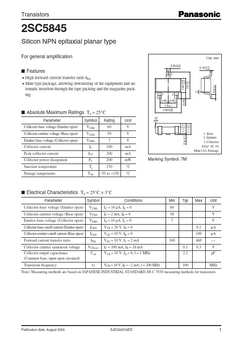
350 300 25°C 250 –25°C 200 150 100 50 0
Forward current transfer ratio hFE
1
10
100
1 000
1
0
8
16
24
32
40
Collector current IC (mA)
Collector-base voltage VCB
SJC00297AED
1
2SC5845
PC Ta
240 50 Ta = 25°C IB = 160 µA 40
IC VCE
140 120 VCE = 10V Ta = 25°C
IC I B
Collector power dissipation PC (mW)
200
Collector current IC (mA)
10˚1.1+0来自2 –0.11.1+0.3 –0.1
1: Base 2: Emitter 3: Collector EIAJ: SC-59 Mini3-G1 Package
Marking Symbol: 7M
■ Electrical Characteristics Ta = 25°C ± 3°C
Parameter Collector-base voltage (Emitter open) Collector-emitter voltage (Base open) Emitter-base voltage (Collector open) Collector-base cutoff current (Emitter open) Collector-emitter cutoff current (Base open) Forward current transfer ratio Collector-emitter saturation voltage Collector output capacitance (Common base, input open circuited) Transition frequency Symbol VCBO VCEO VEBO ICBO ICEO hFE VCE(sat) Cob fT Conditions IC = 10 µΑ, IE = 0 IC = 2 mA, IB = 0 IE = 10 µΑ, IC = 0 VCB = 20 V, IE = 0 VCE = 10 V, IB = 0 VCE = 10 V, IC = 2 mA IC = 100 mA, IB = 10 mA VCB = 10 V, IE = 0, f = 1 MHz VCB = 10 V, IE = −2 mA, f = 200 MHz 160 0.1 2.2 100 Min 60 50 7 0.1 100 460 0.3 Typ Max Unit V V V µA µA V pF MHz
大行车系编号解读
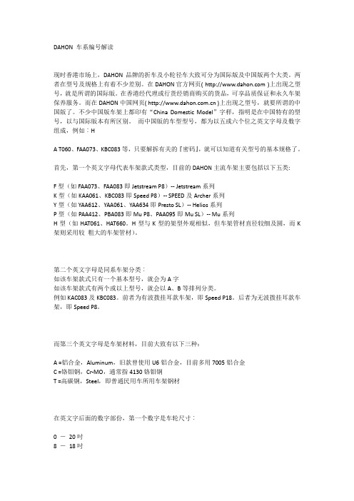
DAHON 车系编号解读现时香港市场上,DAHON品牌的折车及小轮径车大致可分为国际版及中国版两个大类。
两者在型号及规格上有着不少差别。
在DAHON官方网页( )上出现之型号,就是所谓的国际版。
在香港经代理或行货经销商购买的货品,可享品质保证和永久车架保养服务。
而在DAHON中国网页( )上出现之型号,就要所谓的中国版了。
不少中国版车架上都印有“China Domestic Model”字样,指明是在中国特有的型号,以与国际版本有所区别。
而中国版的车型型号,都为以五或六个位之英文字母及数字组成,例如︰HA T060、FAA073、KBC083等,只要解拆有关的『密码』,就可以知道有关型号的基本规格了。
首先,第一个英文字母代表车架款式类型,目前的DAHON主流车架主要包括以下五类:F型(如FAA073、FAA083即Jetstream P8)-- Jetstream系列K型(如KAA061、KBC083即Speed P8)-- SPEED及Archer系列Y型(如YAA612、YAA061、YAA634即Presto SL)-- Helios系列P型(如PAA412、PBA083即Mu P8、PAA095即Mu SL)-- Mu系列H型(如HAT061、HAT660。
H型与K型的架型外观相似,但车架管材直径较细及圆,而K 架则采用较粗大的车架管材)。
第二个英文字母是同系车架分类︰如该车架款式只有一个基本型号,就会为A字如该车架款式有两个或以上型号,就会以A、B等排列分类。
例如KAC083及KBC083。
前者为有波拨挂耳款车架,即Speed P18。
后者为无波拨挂耳款车架,即Speed P8。
而第三个英文字母是车架材料,目前大致有以下三种:A =铝合金,Aluminum,旧款曾使用U6铝合金,目前多用7005铝合金C =铬钼钢,Cr-MO,通常指4130铬钼钢T =高碳钢,Steel,即普通民用车所用车架钢材在英文字后面的数字部份,第一个数字是车轮尺寸︰0 -20吋8 -18吋6 -16吋或26吋5 -16吋4 -14吋2 -12吋第二个数字是变速系统︰1 -单速车3 -3档变速4 -24档变速,即8飞飞轮配内三速軨盒或前三速链饼5 -5档变速6 -6档变速。
CR5842B_中_V1.0

高压启动输入脚,通过启动电阻连接到整流输入电容阳极。
典型应用
EMI Filter
启达科技(香港)有限公司 V1.0
成都启臣微电子有限公司 2/10
CR5842B
结构图
BO
1
HV 8
VTH_BO
VDD 6
Internal supply
LVDD
UVLO
POR
OVP
工作电流
CR5842B 的工作电流为 2mA,这种较低的工作电流和 Burst 模式能够更好的实现效率 的提高与待机功耗的降低,在无负载情况下工作电流进一步降低,保证能够实现超低待机功 耗(50mW 以下)。
软启动
每一次VDD电源启动瞬间,CR5842B芯片内部都将触发软启动功能,即在VDD电压达到 UVLO_OFF以后,在大约4ms时间内,峰值电流从0上升到最大值峰值电流,以减少电源启动 期间功率MOSFET的电压应力。注意:无论何种保护导致的VDD再次启动,都必将触发软 启动功能。
FOSC
PWM工作时频率
高压启动绿色节能反激控制器
测试条件
VDD=2V, HV=100V VDD=18V, HV=500V
最小 典型 最大 单位
2
mA
5 μA
VFB=3V VDD=15V,
VFB=1V
IVDD=10mA
5.0 20.0 μA 2 2.5 mA
0.8 1 mA
13.5 14.5 15.5 V
启达科技(香港)有限公司 V1.0
www.ቤተ መጻሕፍቲ ባይዱ
成都启臣微电子有限公司 7/10
CR5842B
高压启动绿色节能反激控制器
重新充电,但芯片不会重新启动,除非去掉系统电源,且使 VDD 电压下降到 Vth_latch 电 压以下,然后重新供电,系统将重新启动。
UC5842A资料
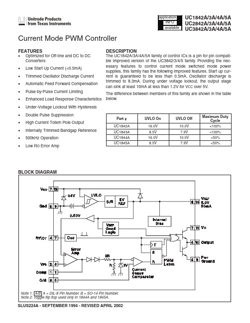
UC1842A/3A/4A/5A UC2842A/3A/4A/5A UC3842A/3A/4A/5A•Optimized for Off-line and DC to DC Converters•Low Start Up Current (<0.5mA)•Trimmed Oscillator Discharge Current •Automatic Feed Forward Compensation •Pulse-by-Pulse Current Limiting•Enhanced Load Response Characteristics •Under-Voltage Lockout With Hysteresis •Double Pulse Suppression •High Current Totem Pole Output •Internally Trimmed Bandgap Reference •500kHz Operation •Low R O Error AmpCurrent Mode PWM ControllerThe UC1842A/3A/4A/5A family of control ICs is a pin for pin compati-ble improved version of the UC3842/3/4/5family.Providing the nec-essary features to control current mode switched mode power supplies,this family has the following improved features.Start up cur-rent is guaranteed to be less than 0.5mA.Oscillator discharge is trimmed to 8.3mA.During under voltage lockout,the output stage can sink at least 10mA at less than 1.2V for V CC over 5V .The difference between members of this family are shown in the table below.FEATURESDESCRIPTIONPart #UVLO On UVLO Off Maximum DutyCycleUC1842A 16.0V 10.0V <100%UC1843A 8.5V 7.9V <100%UC1844A 16.0V 10.0V <50%UC1845A8.5V7.9V<50%UC1842A/3A/4A/5A UC2842A/3A/4A/5AUC3842A/3A/4A/5ACONNECTION DIAGRAMSABSOLUTE MAXIMUM RATINGS (Note 1)Note 1.All voltages are with respect to Ground, Pin 5.Currents are positive into, negative out of the specified terminal.Consult Packaging Section of Databook for thermal limitations and con-siderations of packages.Pin numbers refer to DIL package only.Supply Voltage (Low Impedance Source). . . . . . . . . . . . . .30V Supply Voltage (I CC mA). . . . . . . . . . . . . . . . . . . .Self Limiting Output Current. . . . . . . . . . . . . . . . . . . . . . . . . . . . . . . . . . .±1A Output Energy (Capacitive Load). . . . . . . . . . . . . . . . . . . . .5µJ Analog Inputs (Pins 2, 3). . . . . . . . . . . . . . . . . . .-0.3V to +6.3V Error Amp Output Sink Current . . . . . . . . . . . . . . . . . . . .10mA Power Dissipation at T A ≤25°C (DIL-8). . . . . . . . . . . . . . . .1W Storage Temperature Range. . . . . . . . . . . . . .-65°C to +150°C Lead Temperature (Soldering, 10 Seconds). . . . . . . . . .300°C N/C VREF VCC OUTPUT VCC GND 12345678161514131211N/C N/C N/CRT/CT N/C COMP VFB ISENSE PWRGND N/C109SOIC-WIDE16(TOP VIEW)DW PackagePARAMETERTEST CONDITIONSUC184xA\UC284xA UC384xAUNITSMIN.TYP.MAX.MIN.TYP.MAX.Reference Section Output Voltage T J = 25°C, I O = 1mA 4.955.00 5.05 4.905.00 5.10V Line Regulation 12≤V IN 25V 620620mV Load Regulation 1≤I O ≤20mA 625625mV Temp. Stability(Note 2, Note 7)0.20.40.20.4mV/°C Total Output Variation Line, Load, Temp. 4.95.14.825.18V Output Noise Voltage 10Hz ≤f ≤10kHz T J = 25°C (Note 2)5050µV Long Term Stability T A = 125°C, 1000Hrs. (Note 2)525525mV Output Short Circuit -30-100-180-30-100-180mA Oscillator Section Initial Accuracy T J = 25°C (Note 6)475257475257kHz Voltage Stability 12≤V CC ≤25V0.210.21%Temp. Stability T MIN ≤T A ≤T MAX (Note 2)55%AmplitudeV PIN 4peak to peak (Note 2) 1.7 1.7V Discharge Current T J = 25°C,V PIN 4= 2V (Note 8)7.88.38.87.88.38.8mA V PIN 4= 2V (Note 8)7.58.87.68.8mA Error Amp Section Input VoltageV PIN 1= 2.5V2.45 2.50 2.55 2.42 2.50 2.58V Input Bias Current -0.3-1-0.3-2µA A VOL2≤V O ≤4V65906590dB Unity Gain Bandwidth T J = 25°C (Note 2)0.710.71MHz PSRR12≤V CC ≤25V60706070dB Output Sink Current V PIN 2= 2.7V,V PIN 1= 1.1V 2626mA Output Source Current V PIN 2= 2.3V,V PIN 1= 5V-0.5-0.8-0.5-0.8mA V OUT High V PIN 2= 2.3V,R L = 15k to ground 5656V V OUT LowV PIN 2= 2.7V,R L = 15k to Pin 80.7 1.10.7 1.1V Current Sense Section Gain(Note 3, Note 4) 2.853 3.15 2.853 3.15V/V Maximum Input Signal V PIN 1= 5V (Note 3)0.91 1.10.91 1.1V PSRR12≤V CC ≤25V (Note 3)7070dB Input Bias Current -2-10-2-10µA Delay to Output V PIN 3= 0 to 2V (Note 2)150300150300ns Output Section Output Low Level I SINK = 20mA 0.10.40.10.4V I SINK = 200mA 15 2.215 2.2V Output High Level I SOURCE = 20mA 1313.51313.5V I SOURCE = 200mA1213.51213.5V Rise Time T J = 25°C, C L = 1nF (Note 2)5015050150ns Fall TimeT J = 25°C, C L = 1nF (Note 2)5015050150ns UVLO SaturationV CC = 5V,I SINK = 10mA0.71.20.71.2VELECTRICAL CHARACTERISTICS Unless otherwise stated,these specifications apply for –55°C ≤T A ≤125°C for theUC184xA;–40°C ≤T A ≤125°C for the UC284xAQ;–40°C ≤T A ≤85°C for the UC284xA;0≤T A ≤70°C for the UC384xA;V CC =15V (Note 5);R T =10k;C T =3.3nF;T A =T J ;Pin numbers refer to DIL-8.PARAMETERTEST CONDITIONSUC184xA\UC284xA UC384xAUNITSMIN.TYP.MAX.MIN.TYP.MAX.Under-Voltage Lockout Section Start Threshold x842A/4A 15161714.51617.5V x843A/5A 7.88.49.07.88.49.0V Min. Operation Voltage After x842A/4A 910118.51011.5V Turn On x843A/5A 7.07.68.27.07.68.2V PWM SectionMaximum Duty Cycle x842A/3A 94961009496100%x844A/5A474850474850%Minimum Duty Cycle 00%Total Standby Current Start-Up Current0.30.50.30.5mA Operating Supply Current V PIN 2=V PIN 3= 0V 11171117mA V CC Zener VoltageI CC = 25mA30343034VNote 2:Ensured by design, but not 100% production tested.Note 3:Parameter measured at trip point of latch with V PIN2= 0.Note 4:Gain defined as:A VPIN VPIN =∆∆13;0V PIN 30.8V .Note 5:Adjust V CC above the start threshold before setting at 15V .Note 6:Output frequency equals oscillator frequency for the UC1842A and UC1843A.Output frequency is one half oscillator fre-quency for the UC1844A and UC1845A.Note 7:“Temperature stability, sometimes referred to as average temperature coefficient, is described by the equation:Temp Stability VREF max VREF min TJ max TJ min =−−()()()().V REF (max) and V REF (min) are the maximum & minimum reference volt-age measured over the appropriate temperature range.Note that the extremes in voltage do not necessarily occur at the extremes in temperature.”Note 8:This parameter is measured with R T = 10k to V REF .This contributes approximately 300 A of current to the measurement.The total current flowing into the R T /C pin will be approximately 300 A higher than the measured value.ELECTRICAL CHARACTERISTICS Unless otherwise stated,these specifications apply for –55°C ≤T A ≤125°C for theUC184xA;–40°C ≤T A ≤125°C for the UC284xAQ;–40°C ≤T A ≤85°C for the UC284xA;0≤T A ≤70°C for the UC384xA;V CC =15V (Note 5);R T =10k;C T =3.3nF;T A =T J ;Pin numbers refer to DIL-8.Error Amplifier Open-Loop Frequency ResponseOutput Saturation CharacteristicsUC2842A/3A/4A/5AAPPLICATIONS DATA (cont.)UC2842A/3A/4A/5AUC3842A/3A/4A/5AAPPLICATIONS DATA (cont.)PACKAGING INFORMATIONOrderable Device Status(1)PackageType PackageDrawingPins PackageQtyEco Plan(2)Lead/Ball Finish MSL Peak Temp(3)5962-8670405PA ACTIVE CDIP JG81None A42SNPB Level-NC-NC-NC 5962-8670405VPA ACTIVE CDIP JG81None Call TI Level-NC-NC-NC 5962-8670405VXA ACTIVE LCCC FK201None Call TI Level-NC-NC-NC 5962-8670405XA ACTIVE LCCC FK201None POST-PLATE Level-NC-NC-NC 5962-8670406PA ACTIVE CDIP JG81None A42SNPB Level-NC-NC-NC 5962-8670406VPA ACTIVE CDIP JG81None Call TI Level-NC-NC-NC 5962-8670406VXA ACTIVE LCCC FK201None Call TI Level-NC-NC-NC 5962-8670406XA ACTIVE LCCC FK201None POST-PLATE Level-NC-NC-NC 5962-8670407PA ACTIVE CDIP JG81None A42SNPB Level-NC-NC-NC 5962-8670407VPA ACTIVE CDIP JG81None Call TI Level-NC-NC-NC 5962-8670407VXA ACTIVE LCCC FK201None Call TI Level-NC-NC-NC 5962-8670407XA ACTIVE LCCC FK201None POST-PLATE Level-NC-NC-NC 5962-8670408PA ACTIVE CDIP JG81None A42SNPB Level-NC-NC-NC 5962-8670408VPA ACTIVE CDIP JG81None Call TI Level-NC-NC-NC 5962-8670408VXA ACTIVE LCCC FK201None Call TI Level-NC-NC-NC 5962-8670408XA ACTIVE LCCC FK201None POST-PLATE Level-NC-NC-NC UC1842AJ ACTIVE CDIP JG81None A42SNPB Level-NC-NC-NCUC1842AJ883B ACTIVE CDIP JG81None A42SNPB Level-NC-NC-NCUC1842AJQMLV ACTIVE CDIP JG8None Call TI Call TIUC1842AL883B ACTIVE LCCC FK201None POST-PLATE Level-NC-NC-NCUC1842ALQMLV ACTIVE LCCC FK20None Call TI Call TI UC1843AJ ACTIVE CDIP JG81None A42SNPB Level-NC-NC-NCUC1843AJ883B ACTIVE CDIP JG81None A42SNPB Level-NC-NC-NCUC1843AJQMLV ACTIVE CDIP JG8None Call TI Call TIUC1843AL883B ACTIVE LCCC FK201None POST-PLATE Level-NC-NC-NCUC1843ALQMLV ACTIVE LCCC FK20None Call TI Call TI UC1844AJ ACTIVE CDIP JG81None A42SNPB Level-NC-NC-NCUC1844AJ883B ACTIVE CDIP JG81None A42SNPB Level-NC-NC-NCUC1844AJQMLV ACTIVE CDIP JG8None Call TI Call TIUC1844AL883B ACTIVE LCCC FK201None POST-PLATE Level-NC-NC-NCUC1844ALQMLV ACTIVE LCCC FK20None Call TI Call TI UC1845AJ ACTIVE CDIP JG81None A42SNPB Level-NC-NC-NCUC1845AJ883B ACTIVE CDIP JG81None A42SNPB Level-NC-NC-NCUC1845AJQMLV ACTIVE CDIP JG8None Call TI Call TIUC1845AL883B ACTIVE LCCC FK201None POST-PLATE Level-NC-NC-NCUC1845ALQMLV ACTIVE LCCC FK20None Call TI Call TI UC2842AD ACTIVE SOIC D1450None CU NIPDAU Level-1-220C-UNLIM UC2842AD8ACTIVE SOIC D875None CU NIPDAU Level-1-220C-UNLIM UC2842AD8TR ACTIVE SOIC D82500None CU NIPDAU Level-1-220C-UNLIM UC2842AD8TRG4ACTIVE SOIC D82500None Call TI Call TIUC2842ADTR ACTIVE SOIC D142500None CU NIPDAU Level-1-220C-UNLIM UC2842ADW ACTIVE SOIC DW1640None CU NIPDAU Level-2-220C-1YEAROrderable Device Status(1)PackageType PackageDrawingPins PackageQtyEco Plan(2)Lead/Ball Finish MSL Peak Temp(3)UC2842ADWTR ACTIVE SOIC DW162000None CU NIPDAU Level-2-220C-1YEAR UC2842AJ OBSOLETE CDIP JG8None Call TI Call TIUC2842AN ACTIVE PDIP P850Pb-Free(RoHS)CU SNPB Level-NC-NC-NC UC2843AD ACTIVE SOIC D1450None CU NIPDAU Level-1-220C-UNLIM UC2843AD8ACTIVE SOIC D875None CU NIPDAU Level-1-220C-UNLIM UC2843AD8TR ACTIVE SOIC D82500None CU NIPDAU Level-1-220C-UNLIM UC2843ADTR ACTIVE SOIC D142500None CU NIPDAU Level-1-220C-UNLIM UC2843ADW ACTIVE SOIC DW1640None CU NIPDAU Level-2-220C-1YEAR UC2843ADWTR ACTIVE SOIC DW162000None CU NIPDAU Level-2-220C-1YEAR UC2843AJ OBSOLETE CDIP JG8None Call TI Call TIUC2843AN ACTIVE PDIP P850Pb-Free(RoHS)CU SNPB Level-NC-NC-NC UC2843AQ ACTIVE PLCC FN2046None CU SNPB Level-2-220C-1YEAR UC2844AD ACTIVE SOIC D1450None CU NIPDAU Level-1-220C-UNLIM UC2844AD8ACTIVE SOIC D875None CU NIPDAU Level-1-220C-UNLIM UC2844AD8TR ACTIVE SOIC D82500None CU NIPDAU Level-1-220C-UNLIM UC2844AD8TRG4PREVIEW SOIC D82500None Call TI Call TIUC2844ADTR ACTIVE SOIC D142500None CU NIPDAU Level-1-220C-UNLIM UC2844ADW ACTIVE SOIC DW1640None CU NIPDAU Level-2-220C-1YEAR UC2844ADWTR ACTIVE SOIC DW162000None CU NIPDAU Level-2-220C-1YEAR UC2844AJ ACTIVE CDIP JG81None A42SNPB Level-NC-NC-NC UC2844AN ACTIVE PDIP P850Pb-Free(RoHS)CU SNPB Level-NC-NC-NC UC2844AQD ACTIVE SOIC D1450None Call TI Level-1-220C-UNLIM UC2844AQD8ACTIVE SOIC D875None Call TI Level-1-220C-UNLIM UC2844AQD8R ACTIVE SOIC D82500None Call TI Level-1-220C-UNLIM UC2844AQDR ACTIVE SOIC D142500None Call TI Level-1-220C-UNLIM UC2845AD ACTIVE SOIC D1450None CU NIPDAU Level-1-220C-UNLIM UC2845AD8ACTIVE SOIC D875None CU NIPDAU Level-1-220C-UNLIM UC2845AD8TR ACTIVE SOIC D82500None CU NIPDAU Level-1-220C-UNLIM UC2845AD8TRG4PREVIEW SOIC D82500None Call TI Call TIUC2845ADTR ACTIVE SOIC D142500None CU NIPDAU Level-1-220C-UNLIM UC2845ADW ACTIVE SOIC DW1640None CU NIPDAU Level-2-220C-1YEAR UC2845AN ACTIVE PDIP P850Pb-Free(RoHS)CU SNPB Level-NC-NC-NC UC3842AD ACTIVE SOIC D1450None CU NIPDAU Level-1-220C-UNLIM UC3842AD8ACTIVE SOIC D875None CU NIPDAU Level-1-220C-UNLIM UC3842AD8TR ACTIVE SOIC D82500None CU NIPDAU Level-1-220C-UNLIM UC3842ADTR ACTIVE SOIC D142500None CU NIPDAU Level-1-220C-UNLIM UC3842ADW ACTIVE SOIC DW1640None CU NIPDAU Level-2-220C-1YEAR UC3842ADWTR ACTIVE SOIC DW162000None CU NIPDAU Level-2-220C-1YEAR UC3842AJ ACTIVE CDIP JG81None A42SNPB Level-NC-NC-NC UC3842AN ACTIVE PDIP P850Pb-Free(RoHS)CU SNPB Level-NC-NC-NCOrderable Device Status(1)PackageType PackageDrawingPins PackageQtyEco Plan(2)Lead/Ball Finish MSL Peak Temp(3)UC3842ANG4ACTIVE PDIP P850Green(RoHS&no Sb/Br)CU NIPDAU Level-NA-NA-NAUC3843AD ACTIVE SOIC D1450None CU NIPDAU Level-1-220C-UNLIM UC3843AD8ACTIVE SOIC D875None CU NIPDAU Level-1-220C-UNLIM UC3843AD8G4ACTIVE SOIC D875None Call TI Call TIUC3843AD8TR ACTIVE SOIC D82500None CU NIPDAU Level-1-220C-UNLIM UC3843AD8TRG4ACTIVE SOIC D82500Green(RoHS&no Sb/Br)CU NIPDAU Level-1-260C-UNLIMUC3843ADG4ACTIVE SOIC D1450Green(RoHS&no Sb/Br)CU NIPDAU Level-1-260C-UNLIM UC3843ADTR ACTIVE SOIC D142500None CU NIPDAU Level-1-220C-UNLIM UC3843AJ ACTIVE CDIP JG81None A42SNPB Level-NC-NC-NCUC3843AN ACTIVE PDIP P850Pb-Free(RoHS)CU SNPB Level-NC-NC-NCUC3843ANG4ACTIVE PDIP P850Green(RoHS&no Sb/Br)CU NIPDAU Level-NA-NA-NA UC3844AD ACTIVE SOIC D1450None CU NIPDAU Level-1-220C-UNLIM UC3844AD8ACTIVE SOIC D875None CU NIPDAU Level-1-220C-UNLIM UC3844AD8TR ACTIVE SOIC D82500None CU NIPDAU Level-1-220C-UNLIM UC3844AD8TRG4ACTIVE SOIC D82500Green(RoHS&no Sb/Br)CU NIPDAU Level-1-260C-UNLIM UC3844ADTR ACTIVE SOIC D142500None CU NIPDAU Level-1-220C-UNLIM UC3844ADW ACTIVE SOIC DW1640None CU NIPDAU Level-2-220C-1YEAR UC3844ADWTR ACTIVE SOIC DW162000None CU NIPDAU Level-2-220C-1YEAR UC3844AN ACTIVE PDIP P850Pb-Free(RoHS)CU SNPB Level-NC-NC-NC UC3845AD ACTIVE SOIC D1450None CU NIPDAU Level-1-220C-UNLIM UC3845AD8ACTIVE SOIC D875None CU NIPDAU Level-1-220C-UNLIM UC3845AD8TR ACTIVE SOIC D82500None CU NIPDAU Level-1-220C-UNLIM UC3845ADTR ACTIVE SOIC D142500None CU NIPDAU Level-1-220C-UNLIM UC3845ADW ACTIVE SOIC DW1640None CU NIPDAU Level-2-220C-1YEAR UC3845ADWTR ACTIVE SOIC DW162000None CU NIPDAU Level-2-220C-1YEAR UC3845AJ ACTIVE CDIP JG81None A42SNPB Level-NC-NC-NCUC3845AN ACTIVE PDIP P850Pb-Free(RoHS)CU SNPB Level-NC-NC-NCUC3845ANG4ACTIVE PDIP P850Green(RoHS&no Sb/Br)CU NIPDAU Level-NA-NA-NA(1)The marketing status values are defined as follows:ACTIVE:Product device recommended for new designs.LIFEBUY:TI has announced that the device will be discontinued,and a lifetime-buy period is in effect.NRND:Not recommended for new designs.Device is in production to support existing customers,but TI does not recommend using this part in a new design.PREVIEW:Device has been announced but is not in production.Samples may or may not be available.OBSOLETE:TI has discontinued the production of the device.(2)Eco Plan-May not be currently available-please check /productcontent for the latest availability information and additional product content details.None:Not yet available Lead(Pb-Free).Pb-Free(RoHS):TI's terms"Lead-Free"or"Pb-Free"mean semiconductor products that are compatible with the current RoHS requirementsfor all 6substances,including the requirement that lead not exceed 0.1%by weight in homogeneous materials.Where designed to be soldered at high temperatures,TI Pb-Free products are suitable for use in specified lead-free processes.Green (RoHS &no Sb/Br):TI defines "Green"to mean "Pb-Free"and in addition,uses package materials that do not contain halogens,including bromine (Br)or antimony (Sb)above 0.1%of total product weight.(3)MSL,Peak Temp.--The Moisture Sensitivity Level rating according to the JEDECindustry standard classifications,and peak solder temperature.Important Information and Disclaimer:The information provided on this page represents TI's knowledge and belief as of the date that it is provided.TI bases its knowledge and belief on information provided by third parties,and makes no representation or warranty as to the accuracy of such information.Efforts are underway to better integrate information from third parties.TI has taken and continues to take reasonable steps to provide representative and accurate information but may not have conducted destructive testing or chemical analysis on incoming materials and chemicals.TI and TI suppliers consider certain information to be proprietary,and thus CAS numbers and other limited information may not be available for release.In no event shall TI's liability arising out of such information exceed the total purchase price of the TI part(s)at issue in this document sold by TI to Customer on an annualbasis.PACKAGE OPTION ADDENDUM 10-Mar-2005Addendum-Page 4元器件交易网。
MIC5842中文资料
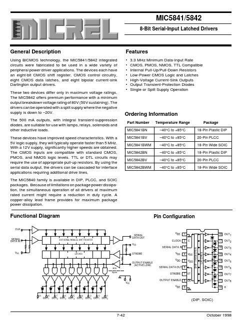
VDD = 12V VDD = 10V VDD = 5.0V (See Note 4) VDD = 12V VDD = 10V VDD = 5.0V All Drivers ON, VDD = 12V All Drivers ON, VDD = 10V All Drivers ON, VDD = 5.0V All Drivers OFF, VDD = 12V All Drivers OFF, VDD = 10V All Drivers OFF, VDD = 5.0V VR = 50V VR = 80V IF = 350mA
Features
• 3.3 MHz Minimum Data-Input Rate • CMOS, PMOS, NMOS, TTL Compatible • Internal Pull-Up/Pull-Down Resistors • Low-Power CMOS Logic and Latches • High-Voltage Current-Sink Outputs • Output Transient-Protection Diodes • Single or Split Supply Operation
EM785840中文资料(ELAN Microelectronics)中文数据手册「EasyDatasheet - 矽搜」
• 两个8位计数器:C1与COUNTER2
• 内置看门狗定时器(WDT)
• 99.9%单指令周期命令
• 三种工作模式(主时钟可以从447.829k被编程为14.3MHz内部产生来自PLL)Mode
CPU状态
主时钟
32.768kHz时钟状态
睡眠模式
关掉
关掉
关掉
绿色模式
打开
关掉
打开
普通模式开启
打开
打开
· 输入端口中断功能
SEG1 SEG0 COM3 COM2 COM1 COM0 AVDD PLLC AVSS
P67 ADR/P66
44 1
43
42
41
40
39
38
37
36
35 3433
2
32
3
31
4
30
5
29
6
28
7
27
8
26
9
25
10
24
1112 13 14 15 16 17 18 19 20 21 2223
PC3 PC2/PWM2 PC1/PWM1 PC0 P70/INT0 P71/INT1 P72/INT2 P73/INT3 P74/SDI P75/SDO P76/SCK
__________________________________________________________________________________________________________________________________________________________________
用户应用笔记
(使用这种芯片之前,先看看下面描述说明,它包含重要信息.)
UCN5842L中文资料
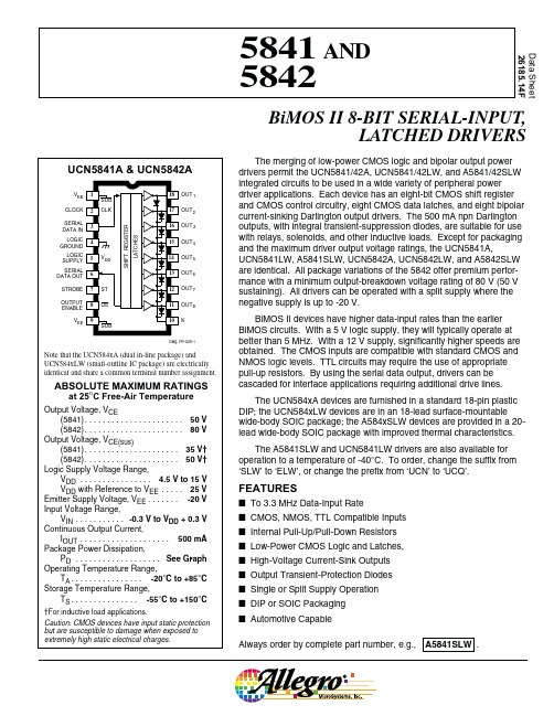
The merging of low-power CMOS logic and bipolar output power drivers permit the UCN5841/42A, UCN5841/42LW, and A5841/42SLW integrated circuits to be used in a wide variety of peripheral power driver applications. Each device has an eight-bit CMOS shift register and CMOS control circuitry, eight CMOS data latches, and eight bipolar current-sinking Darlington output drivers. The 500 mA npn Darlington outputs, with integral transient-suppression diodes, are suitable for use with relays, solenoids, and other inductive loads. Except for packaging and the maximum driver output voltage ratings, the UCN5841A,UCN5841LW, A5841SLW, UCN5842A, UCN5842LW, and A5842SLW are identical. All package variations of the 5842 offer premium perfor-mance with a minimum output-breakdown voltage rating of 80 V (50 V sustaining). All drivers can be operated with a split supply where the negative supply is up to -20 V.BiMOS II devices have higher data-input rates than the earlier BiMOS circuits. With a 5 V logic supply, they will typically operate at better than 5 MHz. With a 12 V supply, significantly higher speeds are obtained. The CMOS inputs are compatible with standard CMOS and NMOS logic levels. TTL circuits may require the use of appropriate pull-up resistors. By using the serial data output, drivers can be cascaded for interface applications requiring additional drive lines.The UCN584xA devices are furnished in a standard 18-pin plastic DIP; the UCN584xLW devices are in an 18-lead surface-mountable wide-body SOIC package; the A584xSLW devices are provided in a 20-lead wide-body SOIC package with improved thermal characteristics.The A5841SLW and UCN5841LW drivers are also available for operation to a temperature of -40°C. To order, change the suffix from ‘SLW’ to ‘ELW’, or change the prefix from ‘UCN’ to ‘UCQ’.FEATURESI To 3.3 MHz Data-Input RateI CMOS, NMOS, TTL Compatible Inputs I Internal Pull-Up/Pull-Down Resistors I Low-Power CMOS Logic and Latches,I High-Voltage Current-Sink Outputs I Output Transient-Protection Diodes I Single or Split Supply Operation I DIP or SOIC Packaging I Automotive CapableBiMOS II 8-BIT SERIAL-INPUT,LATCHED DRIVERSAlways order by complete part number, e.g.,A5841SLW .Data Sheet26185.14F5841 AND 58425841 AND 58428-BIT SERIAL-INPUT,LATCHED DRIVERS115 Northeast Cutoff, Box 15036Worcester, Massachusetts 01615-0036 (508) 853-5000Copyright © 1985, 2000 Allegro MicroSystems, Inc.50751001251502.50.5A L L O W AB L E P AC K A G E P O W E RD I S S I P A T I O N I N W A T T SAMBIENT TEMPERATURE IN °C2.01.51.025Dwg. GP-022-4SERIAL DATA OUT POWER GROUND SERIAL DATA IN OUTPUT ENABLE OUT 1OUT 2OUT 3NOCONNECT.NOCONNECT.LOGIC SUPPLYSTROBE GROUND CLOCK OUT 6OUT 7OUT 8OUT 5OUT 4Dwg. PP-029-3POWER GROUND KA5841SLW & A5842SLW5841 AND 58428-BIT SERIAL-INPUT,LATCHED DRIVERSELECTRICAL CHARACTERISTICS at T A = +25°C, V DD = 5 V, V EE = 0 V (unless otherwise specified).ApplicableLimits CharacteristicSymbol Devices Test ConditionsMin.Max.Unit Output Leakage CurrentI CEX5841*V OUT = 50 V—50µA V OUT = 50 V, T A = +70°C—100µA 5842*V OUT = 80 V—50µA V OUT = 80 V, T A = +70°C—100µA Collector-Emitter V CE(SAT)AllI OUT = 100 mA — 1.1V I OUT = 200 mA— 1.3V I OUT = 350 mA, V DD = 7.0 V— 1.6V Collector-Emitter V CE(sus)5841*I OUT = 350 mA, L = 2 mH 35—V 5842*I OUT = 350 mA, L = 2 mH50—V Input VoltageV IN(0)All —0.8V V IN(1)AllV DD = 12 V 10.5—V V DD = 10 V 8.5—V V DD = 5.0 V3.5—V Input ResistanceR INAllV DD = 12 V 50—k ΩV DD = 10 V 50—k ΩV DD = 5.0 V50—k ΩSupply CurrentI DD(ON)AllAll Drivers ON, V DD = 12 V —16mA All Drivers ON, V DD = 10 V —14mA All Drivers ON, V DD = 5.0 V—8.0mA I DD(OFF)AllAll Drivers OFF, V DD = 12 V — 2.9mA All Drivers OFF, V DD = 10 V — 2.5mA All Drivers OFF, V DD = 5.0 V— 1.6mA Clamp Diode I R5841*V R = 50 V —50µA 5842*V R = 80 V —50µA Clamp Diode V FAllI F = 350 mA—2.0VSaturation VoltageSustaining Voltage Leakage Current Forward Voltage* Complete part number includes a prefix (A or UCN) and a suffix (A, LW, or SLW) as follows:UCN5841A, UCN5841LW, or A5841SLW,UCN5842A, UCN5842LW, or A5842SLW.5841 AND 58428-BIT SERIAL-INPUT,LATCHED DRIVERS115 Northeast Cutoff, Box 15036Worcester, Massachusetts 01615-0036 (508) 853-5000TIMING CONDITIONS(T A = +25°C, V DD = 5.0 V, Logic Levels are V DD and Ground)A.Minimum Data Active Time Before Clock Pulse(Data Set-Up Time) . . . . . . . . . . . . . . . . . . . . . . . . . . . . . . . . . . . . .75 nsB.Minimum Data Active Time After Clock Pulse(Data Hold Time) . . . . . . . . . . . . . . . . . . . . . . . . . . . . . . . . . . . . . . .75 ns C.Minimum Data Pulse Width . . . . . . . . . . . . . . . . . . . . . . . . . . . . . . . . .150 ns D.Minimum Clock Pulse Width . . . . . . . . . . . . . . . . . . . . . . . . . . . . . . . .150 ns E.Minimum Time Between Clock Activation and Strobe . . . . . . . . . . . .300 ns F.Minimum Strobe Pulse Width . . . . . . . . . . . . . . . . . . . . . . . . . . . . . . .100 nsG.Typical Time Between Strobe Activation andOutput Transition . . . . . . . . . . . . . . . . . . . . . . . . . . . . . . . . . . . . .1.0 µsSerial Data present at the input is transferred to the shift register on the logic “0” to logic “1” transition of the CLOCK input pulse. On succeeding CLOCK pulses, the registers shift data information towards the SERIAL DATA OUTPUT. The SERIAL DATA must appear at the input prior to the rising edge of the CLOCK input waveform.Information present at any register is transferred to its respective latch when the STROBE is high (serial-to-parallel conversion). The latches will continue to accept new data as long as the STROBE is held high. Applications where the latches are bypassed (STROBE tied high)will require that the ENABLE input be high during serial data entry.When the ENABLE input is high, all of the output buffers aredisabled (OFF) without affecting the information stored in the latches or shift register. With the ENABLE input low, the outputs are controlled by the state of the latches.CLOCKOUT Dwg. No. A-12,6275841 AND 58428-BIT SERIAL-INPUT,LATCHED DRIVERSTRUTH TABLEL = Low Logic Level H = High Logic Level X = Irrelevant P = Present State R = Previous StateDwg. No. A-12,547UCN5842AThe products described here are manufactured under one or more U.S. patents or U.S. patents pending.Allegro MicroSystems, Inc. reserves the right tomake, from time to time, such departures from the detail specifications as may be required to permit improve-ments in the performance, reliability, ormanufacturability of its products. Before placing an order, the user is cautioned to verify that the informa-tion being relied upon is current.Allegro products are not authorized for use as critical components in life-support devices or systems without express written approval.The information included herein is believed to be accurate and reliable. However, AllegroMicroSystems, Inc. assumes no responsibility for its use; nor for any infringement of patents or other rights of third parties which may result from its use.5841 AND 58428-BIT SERIAL-INPUT,LATCHED DRIVERS115 Northeast Cutoff, Box 15036Worcester, Massachusetts 01615-0036 (508) 853-5000Dwg. MA-001-18A mmUCN5841A and UCN5842ADimensions in Inches (controlling dimensions)Dimensions in Millimeters (for reference only)NOTES:1.Exact body and lead configuration at vendor ’s option within limits shown.2.Lead spacing tolerance is non-cumulative.3.Lead thickness is measured at seating plane or below.Dwg. MA-001-18A in5841 AND 58428-BIT SERIAL-INPUT,LATCHED DRIVERSUCN5841LW and UCN5842LWDimensions in Inches (for reference only)Dimensions in Millimeters (controlling dimensions)NOTES:1.Exact body and lead configuration at vendor ’s option within limits shown.2.Lead spacing tolerance is non-cumulative.Dwg. MA-008-18A inBSCDwg. MA-008-18A mm1.27BSC5841 AND 58428-BIT SERIAL-INPUT,LATCHED DRIVERS115 Northeast Cutoff, Box 15036Worcester, Massachusetts 01615-0036 (508) 853-5000Dwg. MA-008-20 mm1.27BSCA5841SLW and A5842SLWDimensions in Inches (for reference only)Dimensions in Millimeters (controlling dimensions)NOTES:1.Exact body and lead configuration at vendor ’s option within limits shown.2.Lead spacing tolerance is non-cumulative.。
5804中文资料

5804中⽂资料Combining low-power CMOS logic with high-current and high-voltage bipolar outputs, the UCN5804B and UCN5804LB BiMOS II translator/drivers provide complete control and drive for a four-phase unipolar stepper-motor with continuous output current ratings to 1.25 A per phase (1.5 A startup) and 35 V.The CMOS logic section provides the sequencing logic, DIRECTION and OUTPUT ENABLE control, and a power-on reset function. Three stepper-motor drive formats, wave-drive (one-phase), two-phase, and half-step are externally selectable. The inputs are compatible with standard CMOS, PMOS, and NMOS circuits. TTL or LSTTL may require the use of appropriate pull-up resistors to ensure a proper input-logic high.The wave-drive format consists of energizing one motor phase at a time in an A-B-C-D (or D-C-B-A) sequence. This excitation mode consumes the least power and assures positional accuracy regardless of any winding inbalance in the motor. Two-phase drive energizes two adjacent phases in each detent position (AB-BC-CD-DA). This sequence mode offers animproved torque-speed product, greater detent torque, and is less susceptible to motor resonance. Half-step excitation alternates between the one-phase and two-phase modes (A-AB-B-BC-C-CD-D-DA), providing an eight-step sequence.The bipolar outputs are capable of sinking up to 1.5 A and withstanding 50 V in the off state (sustaining voltages up to 35 V). Ground-clamp and flyback diodes provide protection against inductive transients. Thermal protection circuitry disables the outputs when the chip temperature is exces-sive.Both devices are rated for operation over the temperature range of -20°C to +85°C. The UCN5804B is supplied in a 16-pin dual in-line plastic batwing package with a copper lead frame and heat-sinkable tabs for improved power dissipation capabilities; the UCN5804LB is supplied in a 16-lead plastic SOIC batwing package with a copper lead frame and heat-sinkable tabs.FEATURESI 1.5 A Maximum Output Current I 35 V Output Sustaining VoltageI Wave-Drive, Two-Phase, and Half-Step Drive Formats I Internal Clamp DiodesI Output Enable and Direction Control I Power-On ResetI Internal Thermal Shutdown CircuitryBiMOS II UNIPOLARSTEPPER-MOTOR TRANSLATOR/DRIVERAlways order by complete part number, e.g., UCN5804B .Data Sheet 26184.12C*5804115 Northeast Cutoff, Box 15036Worcester, Massachusetts 01615-0036 (508) 853-********BiMOS II UNIPOLAR STEPPER-MOTORTRANSLATOR/DRIVERTRUTH TABLEDrive Format Pin 9Pin 10Two-Phase L L One-Phase H L Half-Step L H Step-InhibitHHTYPICAL INPUT CIRCUITDwg. EP-021-4TYPICAL OUTPUT DRIVERDwg. EP-010-5INCopyright ? 1987, 2000 Allegro MicroSystems, Inc.5075100125150510A L L O W A B L E P A C K A G E P O W E R D I S S I P A T I O N I N W A T T STEMPERATURE IN °C43225Dwg. GP-049-2A5804BiMOS II UNIPOLAR STEPPER-MOTOR TRANSLATOR/DRIVER/doc/a3712eddb9f3f90f76c61b7c.htmlELECTRICAL CHARACTERISTICS at T A = 25°C, T J ≤ 150°C, V DD = 4.5 V to 5.5 V (unless otherwise noted). Limits CharacteristicSymbol Test Conditions Min.Typ.Max.Units Output Leakage Current I CEX V OUT = 50 V—1050µA Output Sustaining Voltage V CE(sus)I OUT = 1.25 A, L = 3 mH 35——V Output Saturation VoltageV CE(SAT)I OUT = 700 mA — 1.0 1.2V I OUT = 1 A — 1.1 1.4V I OUT= 1.25 A— 1.2 1.5V Clamp Diode Leakage Current I R V R = 50 V —1050µA Clamp Diode Forward Voltage V F I F = 1.25 A — 1.53.0V Input CurrentI IN(1)V IN = V DD —0.5 5.0µA I IN(0)V IN = 0.8 V —-0.5-5.0µA Input VoltageV IN(1)V DD = 5 V3.5— 5.3V V IN(0)-0.3—0.8V Supply Current I DD 2 Outputs ON—2030mA Turn-Off Delay t ON 50% Step Inputs to 50% Output ——10µs Turn-On Delayt OFF 50% Step Inputs to 50% Output ——10µs Thermal Shutdown TemperatureT J—165—°CTIMING CONDITIONSA. Minimum Data Set Up Time . . . . . . . . . . . . . . . . . . . . . . . . 100 nsB. Minimum Data Hold Time . . . . . . . . . . . . . . . . . . . . . . . . . . 100 nsC. Minimum Step Input Pulse Width . . . . . . . . . . . . . . . . . . . . . 3.0 µsDwg. W-110AONE PHASE HALF STEPOOUTPUT ENABLEOUTPUT C OUTPUT DCLOCK115 Northeast Cutoff, Box 15036Worcester, Massachusetts 01615-0036 (508) 853-50005804BiMOS II UNIPOLAR STEPPER-MOTORTRANSLATOR/DRIVERWAVE-DRIVE SEQUENCEHalf Step = L, One Phase = H Step A B C D POR ON OFF OFF OFF 1ON OFF OFF OFF 2OFF ON OFF OFF 3OFF OFF ON OFF 4OFFOFFOFFONTWO-PHASE DRIVE SEQUENCEHalf Step = L, One Phase = LStep A B C D POR ON OFF OFF ON 1ON OFF OFF ON 2ON ON OFF OFF 3OFF ON ON OFF 4OFFOFFONONHALF-STEP DRIVE SEQUENCEHalf Step = H, One Phase = LStep A B C D POR ON OFF OFF OFF 1ON OFF OFF OFF 2ON ON OFF OFF 3OFF ON OFF OFF 4OFF ON ON OFF 5OFF OFF ON OFF 6OFF OFF ON ON 7OFF OFF OFF ON 8ONOFFOFFONAPPLICATIONS INFORMATIONInternal power-on reset (POR) circuitry resets OUTPUT A (and OUTPUT D in the two-phase drive format) to the on state with initial applica-tion of the logic supply voltage. After reset, the circuit then steps according to the tables.The outputs will advance one sequenceposition on the high-to-low transition of the STEP INPUT pulse. Logic levels on the HALF-STEP and ONE-PHASE inputs will determine the drive format (one-phase, two-phase, or half-step). The DIRECTION pin determines the rotation se-quence of the outputs. Note that the STEP INPUT must be in the low state when changing the state of ONE-PHASE, HALF-STEP, or DIRECTION to prevent erroneous stepping.All outputs are disabled (off) when OUTPUT ENABLE is at a logic high. If the function is not required, OUTPUT ENABLE should be tied low.In that condition, all outputs depend only on the state of the step logic.During normal commutation of a unipolar stepper motor, mutual coupling between the motor windings can force the outputs of the UCN5804B below ground. This condition will cause forward biasing of the collector-to-substrate junction and source current from the output. For many L/R applications, this substrate current is high enough to adversely affect the logic circuitry and cause misstepping. External series diodes (Schottky are recommended for increasedefficiency at low-voltage operation) will prevent substrate current from being sourced through the outputs. Alternatively, external ground clamp diodes will provide a preferred current path from ground when the outputs are pulled below ground.Internal thermal protection circuitry disables all outputs when the junction temperature reaches approximately 165°C. The outputs are enabled again when the junction cools down to approxi-mately 145°C.5804BiMOS II UNIPOLAR STEPPER-MOTOR TRANSLATOR/DRIVER/doc/a3712eddb9f3f90f76c61b7c.htmlTYPICAL APPLICATION L/R Stepper-Motor DriveThe products described here are manufactured under one or more U.S. patents or U.S. patents pending.Allegro MicroSystems, Inc. reserves the right to make, from time to time, such departures from the detail specifications as may berequired to permit improvements in the performance, reliability, or manufacturability of its products. Before placing an order, the user is cautioned to verify that the information being relied upon is current.Allegro products are not authorized for use as critical components in life-support devices or systems without express written approval.The information included herein is believed to be accurate and reliable. However, Allegro MicroSystems, Inc. assumes no responsi-bility for its use; nor for any infringement of patents or other rights of third parties which may result from its use.115 Northeast Cutoff, Box 15036Worcester, Massachusetts 01615-0036 (508) 853-50005804BiMOS II UNIPOLAR STEPPER-MOTORTRANSLATOR/DRIVERUCN5804BDimensions in Inches (controlling dimensions)Dimensions in Millimeters(for reference only)NOTES:1.Exact body and lead configuration at vendor’s option within limits shown.2.Lead spacing tolerance is non-cumulative.3.Lead thickness is measured at seating plane or below.4.Webbed lead frame. Leads 4, 5, 12, and 13 are internally one piece.5.Supplied in standard sticks/tubes of 25 devices.Dwg. MA-001-17A in18Dwg. MA-001-17A mm185804 BiMOS II UNIPOLAR STEPPER-MOTOR TRANSLATOR/DRIVER/doc/a3712eddb9f3f90f76c61b7c.htmlUCN5804LB(add “TR” to part number for tape and reel) Dimensions in Inches(for reference only)Dimensions in Millimeters(controlling dimensions)NOTES:1.Exact body and lead configuration at vendor’s option within limits shown.2.Lead spacing tolerance is non-cumulative.3.Lead thickness is measured at seating plane or below.4.Webbed lead frame. Leads 4, 5, 12, and 13 are internally one piece.5.Supplied in standard sticks/tubes of 47 devices or add “TR” to part number for tape and reel.115 Northeast Cutoff, Box 15036Worcester, Massachusetts 01615-0036 (508) 853-50005804BiMOS II UNIPOLAR STEPPER-MOTORTRANSLATOR/DRIVERMOTOR DRIVERSFunctionOutput Ratings*Part Number ?INTEGRATED CIRCUITS FOR BRUSHLESS DC MOTORS3-Phase Power MOSFET Controller —28 V 39333-Phase Power MOSFET Controller —50 V 39323-Phase Power MOSFET Controller —50 V 76002-Phase Hall-Effect Sensor/Driver 400 mA 26 V 3626Bidirectional 3-Phase Back-EMFController/Driver ±600 mA 14 V 89062-Phase Hall-Effect Sensor/Driver 900 mA 14 V 36253-Phase Back-EMFController/Driver ±900 mA 14 V 8902–A 3-Phase Controller/Drivers ±2.0 A 45 V 2936 & 2936-120INTEGRATED BRIDGE DRIVERS FOR DC AND BIPOLAR STEPPER MOTORSDual Full Bridge with Protection & Diagnostics ±500 mA 30 V 3976PWM Current-Controlled Dual Full Bridge ±650 mA 30 V 3966PWM Current-Controlled Dual Full Bridge ±650 mA 30 V 3968PWM Current-Controlled Dual Full Bridge ±750 mA 45 V 2916PWM Current-Controlled Dual Full Bridge ±750 mA 45 V 2919PWM Current-Controlled Dual Full Bridge ±750 mA 45 V 6219PWM Current-Controlled Dual Full Bridge ±800 mA 33 V 3964PWM Current-Controlled Full Bridge ±1.3 A 50 V3953PWM Current-Controlled Dual Full Bridge ±1.5 A 45 V 2917PWM Current-Controlled Microstepping Full Bridge ±1.5 A 50 V 3955PWM Current-Controlled Microstepping Full Bridge ±1.5 A 50 V 3957PWM Current-Controlled Dual DMOS Full Bridge ±1.5 A 50 V 3972Dual Full-Bridge Driver ±2.0 A 50 V 2998PWM Current-Controlled Full Bridge ±2.0 A 50 V3952DMOS Full Bridge PWM Driver ±2.0 A 50 V 3958Dual DMOS Full Bridge ±2.5 A 50 V 3971UNIPOLAR STEPPER MOTOR & OTHER DRIVERSVoice-Coil Motor Driver ±500 mA 6 V 8932–A Voice-Coil Motor Driver ±800 mA 16 V 8958Unipolar Stepper-Motor Quad Drivers 1 A 46 V 7024 & 7029Unipolar Microstepper-Motor Quad Driver 1.2 A 46 V 7042Unipolar Stepper-Motor Translator/Driver 1.25 A 50 V 5804Unipolar Stepper-Motor Quad Driver 1.8 A 50 V 2540Unipolar Stepper-Motor Quad Driver 1.8 A 50 V 2544Unipolar Stepper-Motor Quad Driver 3 A 46 V 7026Unipolar Microstepper-Motor Quad Driver 3 A 46 V 7044*Current is maximum specified test condition, voltage is maximum rating. See specification for sustaining voltage limits or over-current protection voltage limits. Negative current is defined as coming out of (sourcing) the output.?Complete part number includes additional characters to indicate operating temperature range and package style.Also, see 3175, 3177, 3235, and 3275 Hall-effect sensors for use with brushless dc motors.。
MAX5841中文资料
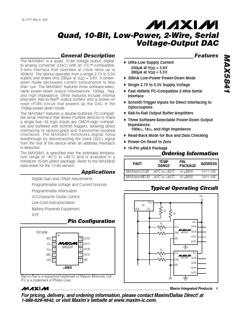
o Rail-to-Rail Output Buffer Amplifiers
o Three Software-Selectable Power-Down Output Impedances 100kΩ, 1kΩ, and High Impedance
ELECTRICAL CHARACTERISTICS
(VDD = +2.7V to +5.5V, GND = 0, VREF = VDD, RL = 5kΩ, CL = 200pF, TA = TMIN to TMAX, unless otherwise noted. Typical values are at VDD = +5V, TA = +25°C.) (Note 1)
元器件交易网
19-1777; Rev 0; 1/02
MAX5841
Quad, 10-Bit, Low-Power, 2-Wire, Serial Voltage-Output DAC
General Description
The MAX5841 is a quad, 10-bit voltage output, digitalto-analog converter (DAC) with an I2C™-compatible, 2-wire interface that operates at clock rates up to 400kHz. The device operates from a single 2.7V to 5.5V supply and draws only 230µA at VDD = 3.6V. A powerdown mode decreases current consumption to less than 1µA. The MAX5841 features three software-selectable power-down output impedances: 100kΩ, 1kΩ, and high impedance. Other features include internal precision Rail-to-Rail® output buffers and a power-on reset (POR) circuit that powers up the DAC in the 100kΩ power-down mode. The MAX5841 features a double-buffered I2C-compatible serial interface that allows multiple devices to share a single bus. All logic inputs are CMOS-logic compatible and buffered with Schmitt triggers, allowing direct interfacing to optocoupled and transformer-isolated interfaces. The MAX5841 minimizes digital noise feedthrough by disconnecting the clock (SCL) signal from the rest of the device when an address mismatch is detected.
SM5844资料
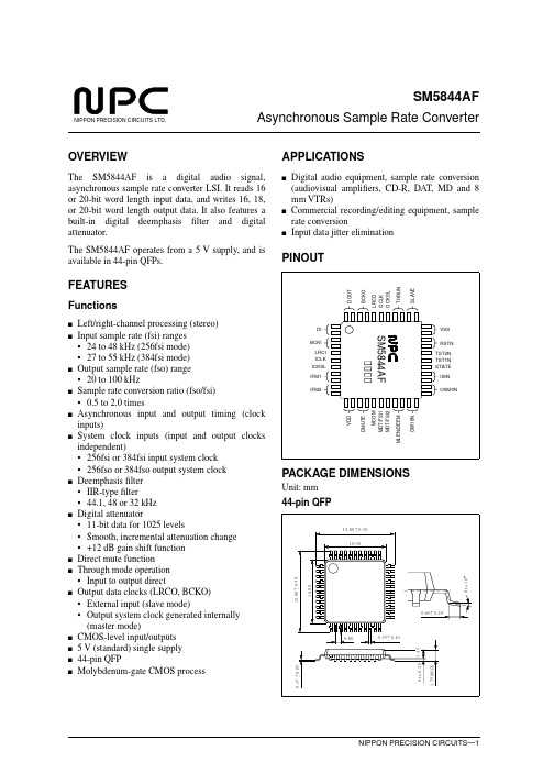
106 dB 109 dB
NIPPON PRECISION CIRCUITS—2
SM5844AF
BLOCK DIAGRAM
IFM1 IFM2 BCKI DI
MCOM MDT/FSI1 MCK/FSI2 MLEN/DEEM Deemphasis and attenuator setup
Input data interface
Mode 1 2 3 4 5 6 W ord length 16 bits 18 bits 20 bits 20 bits 16 bits Front 18 bits 20 bits IIS 7 Nor mal (non IIS) Rear IIS selection Front/rear p a cking
Mode 1 2 3 4 20 bits Front Rear LSB first W ord length 16 bits Rear M S B fi rst Front/rear p a cking Data sequence
s
Output data format • 2s-complement, MSB first, L/R alternating, serial • Continuous bit clock
TST1N TST2N Output operation timing controller Output operation
OW18N OW20N IISN Output format controller
Dither Output data interface
SLAVE
Output-stage clock selectຫໍສະໝຸດ 17MDT/FSI1
Ip
19, 20
AD584S资料
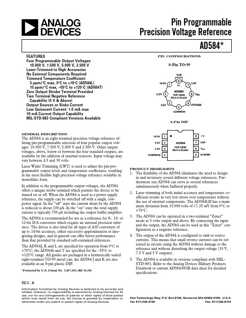
One Technology Way, P.O. Box 9106, Norwood, MA 02062-9106, U.S.A.
Tel: 617/329-4700
Fax: 617/326-8703
元器件交易网
AD584–SPECIFICATIONS (@ VIN = +15 V and 25؇C)
4. The output of the AD584 is configured to sink or source currents. This means that small reverse currents can be tolerated Байду номын сангаасn circuits using the AD584 without damage to the reference and without disturbing the output voltage (10 V, 7.5 V and 5 V outputs).
3. The AD584 can be operated in a two-terminal “Zener” mode at 5 volts output and above. By connecting the input and the output, the AD584 can be used in this “Zener” configuration as a negative reference.
REV. A
Information furnished by Analog Devices is believed to be accurate and reliable. However, no responsibility is assumed by Analog Devices for its use, nor for any infringements of patents or other rights of third parties which may result from its use. No license is granted by implication or otherwise under any patent or patent rights of Analog Devices.
2SJ584LS资料
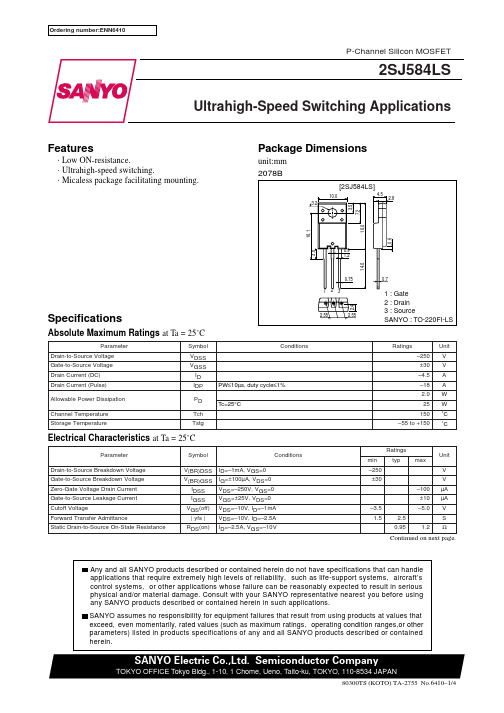
SANYO Electric Co.,Ltd. Semiconductor Company
TOKYO OFFICE Tokyo Bldg., 1-10, 1 Chome, Ueno, Taito-ku, TOKYO, 110-8534 JAPAN
80300TS (KOTO) TA-2755 No.6410–1/4
Ciss
td(on)
Coss
Crss
Drain Current, ID – A
--1.0
--10
--20
--25
--30 IT01504
IT01503 --100 7 5 3 2
Drain-to-Source Voltage, VDS – V
--10 --9
VGS -- Qg
VDS= --100V ID= --4.5A Drain Current, ID – A
IT01505 40
Drain-to-Source Voltage, VDS – V
7 --10
2
3
5 7 --100
2
3
5 7 --1000 IT01506
2.5
PD -- Ta
Allowable Power Dissipation, PD – W
Drain Current, ID – A
75°C
--6 --5 --4 --3 --2 --1
--6V
--5V
0
Drain-to-Source Voltage, VDS – V
--3
--4
--5
--6
--7
--8
--9
--10
0
--1
--2
--9
- 1、下载文档前请自行甄别文档内容的完整性,平台不提供额外的编辑、内容补充、找答案等附加服务。
- 2、"仅部分预览"的文档,不可在线预览部分如存在完整性等问题,可反馈申请退款(可完整预览的文档不适用该条件!)。
- 3、如文档侵犯您的权益,请联系客服反馈,我们会尽快为您处理(人工客服工作时间:9:00-18:30)。
The merging of low-power CMOS logic and bipolar output power drivers permit the UCN5841/42A, UCN5841/42LW, and A5841/42SLW integrated circuits to be used in a wide variety of peripheral power driver applications. Each device has an eight-bit CMOS shift register and CMOS control circuitry, eight CMOS data latches, and eight bipolar current-sinking Darlington output drivers. The 500 mA npn Darlington outputs, with integral transient-suppression diodes, are suitable for use with relays, solenoids, and other inductive loads. Except for packaging and the maximum driver output voltage ratings, the UCN5841A,UCN5841LW, A5841SLW, UCN5842A, UCN5842LW, and A5842SLW are identical. All package variations of the 5842 offer premium perfor-mance with a minimum output-breakdown voltage rating of 80 V (50 V sustaining). All drivers can be operated with a split supply where the negative supply is up to -20 V.BiMOS II devices have higher data-input rates than the earlier BiMOS circuits. With a 5 V logic supply, they will typically operate at better than 5 MHz. With a 12 V supply, significantly higher speeds are obtained. The CMOS inputs are compatible with standard CMOS and NMOS logic levels. TTL circuits may require the use of appropriate pull-up resistors. By using the serial data output, drivers can be cascaded for interface applications requiring additional drive lines.The UCN584xA devices are furnished in a standard 18-pin plastic DIP; the UCN584xLW devices are in an 18-lead surface-mountable wide-body SOIC package; the A584xSLW devices are provided in a 20-lead wide-body SOIC package with improved thermal characteristics.The A5841SLW and UCN5841LW drivers are also available for operation to a temperature of -40°C. To order, change the suffix from ‘SLW’ to ‘ELW’, or change the prefix from ‘UCN’ to ‘UCQ’.FEATURESI To 3.3 MHz Data-Input RateI CMOS, NMOS, TTL Compatible Inputs I Internal Pull-Up/Pull-Down Resistors I Low-Power CMOS Logic and Latches,I High-Voltage Current-Sink Outputs I Output Transient-Protection Diodes I Single or Split Supply Operation I DIP or SOIC Packaging I Automotive CapableBiMOS II 8-BIT SERIAL-INPUT,LATCHED DRIVERSAlways order by complete part number, e.g.,A5841SLW .Data Sheet26185.14F5841 AND 58425841 AND 58428-BIT SERIAL-INPUT,LATCHED DRIVERS115 Northeast Cutoff, Box 15036Worcester, Massachusetts 01615-0036 (508) 853-5000Copyright © 1985, 2000 Allegro MicroSystems, Inc.50751001251502.50.5A L L O W AB L E P AC K A G E P O W E RD I S S I P A T I O N I N W A T T SAMBIENT TEMPERATURE IN °C2.01.51.025Dwg. GP-022-4SERIAL DATA OUT POWER GROUND SERIAL DATA IN OUTPUT ENABLE OUT 1OUT 2OUT 3NOCONNECT.NOCONNECT.LOGIC SUPPLYSTROBE GROUND CLOCK OUT 6OUT 7OUT 8OUT 5OUT 4Dwg. PP-029-3POWER GROUND KA5841SLW & A5842SLW5841 AND 58428-BIT SERIAL-INPUT,LATCHED DRIVERSELECTRICAL CHARACTERISTICS at T A = +25°C, V DD = 5 V, V EE = 0 V (unless otherwise specified).ApplicableLimits CharacteristicSymbol Devices Test ConditionsMin.Max.Unit Output Leakage CurrentI CEX5841*V OUT = 50 V—50µA V OUT = 50 V, T A = +70°C—100µA 5842*V OUT = 80 V—50µA V OUT = 80 V, T A = +70°C—100µA Collector-Emitter V CE(SAT)AllI OUT = 100 mA — 1.1V I OUT = 200 mA— 1.3V I OUT = 350 mA, V DD = 7.0 V— 1.6V Collector-Emitter V CE(sus)5841*I OUT = 350 mA, L = 2 mH 35—V 5842*I OUT = 350 mA, L = 2 mH50—V Input VoltageV IN(0)All —0.8V V IN(1)AllV DD = 12 V 10.5—V V DD = 10 V 8.5—V V DD = 5.0 V3.5—V Input ResistanceR INAllV DD = 12 V 50—k ΩV DD = 10 V 50—k ΩV DD = 5.0 V50—k ΩSupply CurrentI DD(ON)AllAll Drivers ON, V DD = 12 V —16mA All Drivers ON, V DD = 10 V —14mA All Drivers ON, V DD = 5.0 V—8.0mA I DD(OFF)AllAll Drivers OFF, V DD = 12 V — 2.9mA All Drivers OFF, V DD = 10 V — 2.5mA All Drivers OFF, V DD = 5.0 V— 1.6mA Clamp Diode I R5841*V R = 50 V —50µA 5842*V R = 80 V —50µA Clamp Diode V FAllI F = 350 mA—2.0VSaturation VoltageSustaining Voltage Leakage Current Forward Voltage* Complete part number includes a prefix (A or UCN) and a suffix (A, LW, or SLW) as follows:UCN5841A, UCN5841LW, or A5841SLW,UCN5842A, UCN5842LW, or A5842SLW.5841 AND 58428-BIT SERIAL-INPUT,LATCHED DRIVERS115 Northeast Cutoff, Box 15036Worcester, Massachusetts 01615-0036 (508) 853-5000TIMING CONDITIONS(T A = +25°C, V DD = 5.0 V, Logic Levels are V DD and Ground)A.Minimum Data Active Time Before Clock Pulse(Data Set-Up Time) . . . . . . . . . . . . . . . . . . . . . . . . . . . . . . . . . . . . .75 nsB.Minimum Data Active Time After Clock Pulse(Data Hold Time) . . . . . . . . . . . . . . . . . . . . . . . . . . . . . . . . . . . . . . .75 ns C.Minimum Data Pulse Width . . . . . . . . . . . . . . . . . . . . . . . . . . . . . . . . .150 ns D.Minimum Clock Pulse Width . . . . . . . . . . . . . . . . . . . . . . . . . . . . . . . .150 ns E.Minimum Time Between Clock Activation and Strobe . . . . . . . . . . . .300 ns F.Minimum Strobe Pulse Width . . . . . . . . . . . . . . . . . . . . . . . . . . . . . . .100 nsG.Typical Time Between Strobe Activation andOutput Transition . . . . . . . . . . . . . . . . . . . . . . . . . . . . . . . . . . . . .1.0 µsSerial Data present at the input is transferred to the shift register on the logic “0” to logic “1” transition of the CLOCK input pulse. On succeeding CLOCK pulses, the registers shift data information towards the SERIAL DATA OUTPUT. The SERIAL DATA must appear at the input prior to the rising edge of the CLOCK input waveform.Information present at any register is transferred to its respective latch when the STROBE is high (serial-to-parallel conversion). The latches will continue to accept new data as long as the STROBE is held high. Applications where the latches are bypassed (STROBE tied high)will require that the ENABLE input be high during serial data entry.When the ENABLE input is high, all of the output buffers aredisabled (OFF) without affecting the information stored in the latches or shift register. With the ENABLE input low, the outputs are controlled by the state of the latches.CLOCKOUT Dwg. No. A-12,6275841 AND 58428-BIT SERIAL-INPUT,LATCHED DRIVERSTRUTH TABLEL = Low Logic Level H = High Logic Level X = Irrelevant P = Present State R = Previous StateDwg. No. A-12,547UCN5842AThe products described here are manufactured under one or more U.S. patents or U.S. patents pending.Allegro MicroSystems, Inc. reserves the right tomake, from time to time, such departures from the detail specifications as may be required to permit improve-ments in the performance, reliability, ormanufacturability of its products. Before placing an order, the user is cautioned to verify that the informa-tion being relied upon is current.Allegro products are not authorized for use as critical components in life-support devices or systems without express written approval.The information included herein is believed to be accurate and reliable. However, AllegroMicroSystems, Inc. assumes no responsibility for its use; nor for any infringement of patents or other rights of third parties which may result from its use.5841 AND 58428-BIT SERIAL-INPUT,LATCHED DRIVERS115 Northeast Cutoff, Box 15036Worcester, Massachusetts 01615-0036 (508) 853-5000Dwg. MA-001-18A mmUCN5841A and UCN5842ADimensions in Inches (controlling dimensions)Dimensions in Millimeters (for reference only)NOTES:1.Exact body and lead configuration at vendor ’s option within limits shown.2.Lead spacing tolerance is non-cumulative.3.Lead thickness is measured at seating plane or below.Dwg. MA-001-18A in5841 AND 58428-BIT SERIAL-INPUT,LATCHED DRIVERSUCN5841LW and UCN5842LWDimensions in Inches (for reference only)Dimensions in Millimeters (controlling dimensions)NOTES:1.Exact body and lead configuration at vendor ’s option within limits shown.2.Lead spacing tolerance is non-cumulative.Dwg. MA-008-18A inBSCDwg. MA-008-18A mm1.27BSC5841 AND 58428-BIT SERIAL-INPUT,LATCHED DRIVERS115 Northeast Cutoff, Box 15036Worcester, Massachusetts 01615-0036 (508) 853-5000Dwg. MA-008-20 mm1.27BSCA5841SLW and A5842SLWDimensions in Inches (for reference only)Dimensions in Millimeters (controlling dimensions)NOTES:1.Exact body and lead configuration at vendor ’s option within limits shown.2.Lead spacing tolerance is non-cumulative.。
