AC05P020中文资料
PQ05RF2_01资料
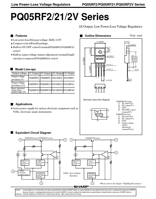
PQ05RF2Vseries
VIN
1
0.33µF
2 3.3µF
VO
+
4
A IO
3
+
V
47µF A Iq
RL
Fig. 2 Test Circuit of Ripple Rejection
PQ05RF2/PQ05RF21series
PQ05RF2Vseries
1 ei
VIN 0.33µF
+
2
1
4
ei
+
3
(Unless otherwise specified, condition shall be Io=1A, Ta=25˚C, ❇3)
Parameter
PQ05RF2/PQ05RF2V
PQ09RF2/PQ09RF2V
PQ12RF2/PQ12RF2V
Output voltage
PQ15RF2/PQ15RF2V PQ05RF21
元器件Lo交w P易o网wewr-wLwos.cseVcbo2ltba.gcoemRegulators
Fig. 1 Test Circuit
PQ05RF2/PQ05RF21series
VIN
1
0.33µF
2
47µF VO
4 VC
A IO
3
+
A
V
A Iq
IC
RL
PQ05RF2/PQ05RF21/PQ05RF2V Series
−
MIN.
4.75 8.55 11.4 14.25 4.88 8.78 11.7 14.63
− − − 45 55 − 2.0 ❇6 − − − − 4.5 8.1 10.8 13.5
MPC2005中文资料
MPC2004•MPC20056–1Advance Information256KB and 512KB BurstRAM ™Secondary Cache Modules for PowerPC ™ PReP/CHRP PlatformsThe MPC2004 and MPC2005 are designed to provide burstable, high perfor-mance 256KB/512KB L2 cache for the PowerPC 60x microprocessor family in conformance with the PowerPC Reference Platform (PReP) and the PowerPC Common Hardware Reference Platform (CHRP) specifications. The modules are configured as 32K x 72 and 64K x 72 bits in a 182 (91 x 2) pin DIMM format.Each module uses four of Motorola’s 5 V 32K x 18 or 64K x 18 BurstRAMs and a 5 V cache tag RAM configured as 16K x 12 for tag field plus 16K x 2 for valid and dirty status bits.es are generated internal to the BurstRAM by the SRAMCNTEN signal.Write cycles are internally self timed and are initiated by the rising edge of the clock (CLKx) inputs. Eight write enables are provided for byte write control.Presence detect pins are available for auto configuration of the cache control.A serial EEPROM is optional to provide more in–depth description of the cache module.The module family pinout will support 5 V and 3.3 V components for a clear path to lower voltage and power savings. Both power supplies must be connected.These cache modules are plug and pin compatible with the MPC2006, a 1MB synchronous module also designed for the PReP and CHRP specifications.They are also compatible with the MPC2007 and MPC2009, 256KB and 1MB re-spectively, asynchronous cache modules.•PowerPC–style Burst Counter on Chip •Flow–Through Data I/O•Module Requires Both 3.3 V and 5 V Power Supplies •Multiple Clock Pins for Reduced Loading•All Cache Data and T ag I/Os are LVTTL (3.3 V) Compatible •Three State Outputs •Byte Write Capability•Fast Module Clock Rates: 66 MHz•Fast SRAM Access Times: 10 ns for Tag RAM Match9 ns for Data RAM •Decoupling Capacitors for Each Fast Static RAM•High Quality Multi–Layer FR4 PWB With Separate Power and Ground Planes •182 Pin Card Edge Module•Burndy Connector, Part Number: ELF182JSC–3Z50BurstRAM is a trademark of Motorola.BurstRAM is a trademark of Motorola.PowerPC is a trademark of International Business Machines Corp.This document contains information on a new product. Specifications and information herein are subject to change without notice.Order this documentby MPC2004/DMOTOROLASEMICONDUCTOR TECHNICAL DATAMPC2004MPC2005associated with such unintended or unauthorized use, even if such claim alleges that Motorola was negligent regarding the design or manufacture of the part. Motorola and。
日本山洋—中文AC伺服R+P样本
电源高次谐波对策
标准装备有DC扼流圈连接端子作为电源高次谐波对策 用。
AC SERVO AMPLIFIER
R
RS1A100A
MODE
/WR
T S R t r
DL1 DL1 DL2
DL2 P RB1 RB2
CHARGE
POWER
P C
C N A
R
AC SERVO AMPLIFIER
C N 1
C N B
传感器组合种类 01 ·· 省配线型增量编码器
適用馬達編碼 P1系列
1B‥‥‥ P10B13100B 1C‥‥‥ P10B13150B 1D‥‥‥ P10B18200B
P5系列
M3‥‥‥ P50B04010D M5‥‥‥ P50B05020D MT‥‥‥ P50B07040H MF‥‥‥ P50B08075H MG‥‥‥ P50B08100H
自动调谐
通过采用了新算法的惯性恒等功能和5种自动调谐特 性选择、30级响应性设定或利用参数的自动保存功 能,可实现提高响应性的自动调谐。
试运转功能(微动功能)
搭载有能够确认马达和放大器间连接的微动功能,不 必与上位装置连接,便能进行试运转。
速度指令值
调谐开始
速度检出值
AC SERVO AMPLIFIER
C
参数的设定 位置、速度和转矩监控波形
˞
※PC计算机连接用电缆 型号:AL-00490833-01 (任选件)
4
可提高系统的精度,并缩短周期时间
高响应
使用能减小相位滞后的4级陷波滤波器,可以抑制机 械系统的共振,并提高装置的速度响应性。
减振控制
利用前馈减振控制,可通过简单的调整来抑制机械前 端的振动和机架的振动。 同时,能够设定并选择使用4种用以控制振动的频率。
LD05-20BxxMU系列AC DC转换器用户说明书
5W, AC/DC converterRoHSFEATURES● Universal input: 85~264V AC/100~370VDC● AC and DC dual-use (input from the same terminal) ● High efficiency, high power density● Output short-circuit, over-current, over-voltage protection ● EN60601-1, ANSI/AAMI ES60601-1 approval (3rd edition 2xMOPP)LD05-20BxxMU series is a compact size power converter. It features universal input voltage, taking both DC and AC input voltage, low power consumption, high efficiency, high reliability, safer isolation. It offers good EMC performance, and is widely used in medical, industrial and instrumentation applications.Selection GuideRS Stock No. Part No. Output PowerNominal Output V oltageand Current (V o/Io)Efficiency (230V AC, %/Typ.)Max. Capacitive Load*(µF)1446281 LD05-20B05MU 5W 5V/1000mA 76 4000 1446282 LD05-20B12MU 12V/420mA 80 820 1446283 LD05-20B24MU5.5W24V/230mA81330Note: *Test without external circuit.Input SpecificationsItemOperating Conditions Min. Typ. Max. Unit Input V oltage Range AC input 85 -- 264 V AC DC input 100 -- 370 VDC Input frequency 47 -- 63 HzInput current115V AC -- -- 0.12 A 230V AC -- -- 0.07 Inrush current 115V AC -- 10 -- 230V AC -- 20 -- Leakage Current264V AC ----80uA Recommended external input fuse2A/250V , slow blowOutput SpecificationsItemOperating Conditions Min. Typ. Max. UnitOutput V oltage Accuracy-- ±2 -- % Line Regulation Full load -- ±0.5 -- Load Regulation 10%-100% load-- ±1 -- Ripple & Noise* 20MHz bandwidth (peak-peak value)-- 50 100 mV Temperature Coefficient -- ±0.02 -- %/℃ Stand-by Power Consumption----0.3W Short Circuit Protection Continuous, self-recovery Over-current Protection110 - 280% Io self-recoveryOver-voltage Protection LD05-20B05MU -- -- 7.5 VLD05-20B12MU -- -- 16 LD05-20B24MU-- -- 30 Min. Load0 -- -- % Hold-up Time115V AC input -- 10 -- ms 230V AC input --80--General SpecificationsItem Operating Conditions Min. Typ. Max. Unit Isolation V oltage Input-output Test time: 1min 4000 -- -- V AC Operating Temperature -25 -- +70℃Storage Temperature -40 -- +85Max. Casing Temperature -- -- +95Storage Humidity -- -- 95 %RHWelding Temperature Wave-soldering 260±5℃; time:5~10s Manual-welding 360±10℃; time:3~5sSwitching Frequency -- -- 140 kHzPower Derating -25 ~ 0℃ 1 -- -- %/℃+55 ~ +70℃ 2 -- -- %/℃Safety Standard EN60601/UL60601Safety Certification EN60601/UL60601Safety Class CLASS IIinsulation Level Primary to Secondary2xMOPPMTBF MIL-HDBK-217F@25℃ >300,000 h Physical SpecificationsCasing Material Black flame-retardant and heat-resistant plastic (UL94-V0)Package Dimensions 53.80*28.80*19.00 mmWeight 43g (Typ.)Cooling method Free air convectionEMC SpecificationsEMI CE CISPR11/EN55011 CLASS B RE CISPR11/EN55011 CLASS BEMS ESD IEC/EN61000-4-2 Contact±6KV/Air±8KV Perf. Criteria B RS IEC/EN61000-4-3 10V/m perf. Criteria AEFTIEC/EN61000-4-4 ±2KV perf. Criteria BIEC/EN61000-4-4 ±4KV (See Fig. 2 for recommended circuit) perf. Criteria B SurgeIEC/EN61000-4-5 ±1KV perf. Criteria BIEC/EN61000-4-5 ±2KV/±4KV (See Fig. 2 for recommended circuit) perf. Criteria B CS IEC/EN61000-4-6 10 Vr.m.s perf. Criteria A PFM IEC/EN61000-4-8 10A/m perf. Criteria A V oltage dips, short interruptions andvoltage variations immunityIEC/EN61000-4-11 0%-70% perf. Criteria BProduct Characteristic Curve-25 0 55 701007075O u t p u t P o w e r P e r c e n t a g e (%)Amb ie nt T e mp e ra ture ()℃T empe rature Dera ting Curve100~264VAC 120~370VDCInp ut vo lta g e:1007010085264120100370VAC VD C240340Input Volta ge De ra ting CurveAmb ie nt te m p e ra ture :25℃Inp ut Vo lta g eO u t p u t P o w e r P e r c e n t a g e (%)Note: Input voltage should be derated based on temperature derating when it is 85~100VAC/100~120VDC;This product is suitable for use in natural air cooling environments, if in a closed environment, please contact our company’s FAE.L D05-20B05MU50 55 6065 70 75 80 85 9095 100 85V110V120V220V240V264VE f f i c i e n c y (%)Input Voltage(V)E fficiency Vs Input Voltage (F ull L oad)L D05-20B05MU5055 6065 70 75 808590 10254050657590100E f f i c i e n c y (%)Output Cur r ent Per centage(%)E fficiency Vs Output L oad(Vin=230VAC)L D05-20B24MU50 556065 70 75 80 859095 100 85V110V120V220V240V264VE f f i c i e n c y (%)Input Voltage(V)E fficiency Vs Input Voltage (F ull L oad)L D05-20B24MU5055 6065 70 75 808590 10254050657590100E f f i c i e n c y (%)Output Cur r ent Per centage(%)E fficiency Vs Output L oad(Vin=230VAC)Design Reference1. T ypical application circuitAC (L )+Vo-VoA C (L )AC (N)AC(N)C 1C 2L O ADF US E AC /DCM O VN T CFig. 1: Typical application circuitModelC1(µF) C2(µF) LD05-20B05MU 1220 LD05-20B12MU 100 LD05-20B24MU47Note:Output filtering capacitor C2 is electrolytic capacitor, it is recommended to apply electrolytic capacitor with high frequency and low resistance. For capacitance and current of capacitor please refer to manufacture’s datasheet. Capacitance withstand voltage derating should be 80% or above. C1 is ceramic capacitor, which is used to filter high-frequency noise. External input NTC is recommended to use 5D-9. External input MOV is recommended to use S14K300. External input FUSE is recommended to use 2A/250V , slow blow.2. E MC solution-recommended circuitAC DCAC (N)AC (L)LCMM OVC XC Y1C Y2FUSEAC (N)AC (L)+Vo-Vo+L1C1C2R LC a n us e MO RNS UN’s FC -L X1DNT CFig 2: EMC Recommended circuit with higher requirementsElement modelRecommended valueMOV S14K300 CX 0.1µF/275V AC L1 4.7uH/2.0A CY1 1nF/400V AC CY2 1nF /400V ACNTC 5D-9LCM 2.2mH, recommended to use MORNSUN’s FL2D -10-222FUSE 2A/250V , slow blow, necessaryFC-LX1DEMC FilterDimensions and Recommended LayoutNote:1.If the product is not operated within the required load range, the product performance cannot be guaranteed to comply with all parameters in the datasheet;2.Unless otherwise specified, parameters in this datasheet were measured under the conditions of Ta = 25℃, humidity <75% with nominal input voltage andrated output load;3.All index testing methods in this datasheet are based on our Company’s corporate stan dards;4.The performance parameters of the product models listed in this manual are as above, but some parameters of non-standard model products may exceed therequirements mentioned above. Please contact our technicians directly for specific information;5.We can provide product customization service;6.Specifications are subject to change without prior notice.。
康沃FSCG05P05变频器说明书

Convo 变频器 2013u VFC 2600u FSCS01u FSCG05u FSCZ01/Z02博世力士乐 (西安)电子传动与控制有限公司2产品采用高性能功率模块,确保设备运行稳定可靠;高速微电脑芯片配以高效的专业控制软件,保证设备始终运行在最佳状态;壳体和配件由数控设备自动完成加工,美观坚固;引入ISO9001质量体系,最大化消除质量隐患,承诺提供给客户最优的产品。
Convo 在解决变频器各种应用问题方面是您强大的合作伙伴。
我公司高能效的变频器产品可以提供精准的程序及速度调控,为您实现可观的能源减耗。
作为博世力士乐品牌家族的成员,我们始终致力于为我们的客户呈递高品质的变频器产品。
3公司介绍博世力士乐 (西安) 电子传动与控制有限公司致力于在中国工控传动领域发展,这也是博世力士乐未来在中国工控传动领域成功的重要保证。
博世力士乐 (西安) 电子传动与控制有限公司是德国博世集团的全资子公司。
力士乐是独一无二的,因为在世界市场上,没有其他的品牌能向顾客提供所有的传动与控制技术。
专业化与一体化并举,正因如此,我们在驱动、控制及运动控制技术等领域成为了世界性的榜样。
所有这一切既给予我们鼓舞,也赋予我们责任。
博世力士乐,The Drive & Control Company,独一无二。
4节能目前Convo系列变频器在中国区域内应用于众多行业,如纺织、印染、冶金、电力、石油、化工、建筑楼宇、市政、建材、机床等,其应用节能率在风机、水泵行业尤其突出,另外在球磨机、空压机、注塑机、压铸机等专用设备上也非常明显,节能率最高可达到60 %。
5系列产品技术指标Convo6VFC 2600系列变频器玲珑实惠、简单可靠功能强大的迷你变频器单相220 V 0.4-2.2 kW三相380 V 0.4-4.0 kW产品特点玲珑n比以往产品小40 %n零距离无缝并排安装,节省安装空间实惠n高性价比,内置PID,内置制动单元n高过载能力,无需增档使用n高节能率,省电30 %n高利用率,面板可拆卸,切换使用简单n操作便捷,参数可复制n维护容易,风扇可自由拆卸,1.5 kW以下自冷散热n调试方便,结构化参数组n功能智能,自动限流,自/手动转矩提升,转速捕获可靠n卓越品质来自博世标准生产系统n系统的安规和可靠性测试n保护完善 (缺相、相间短路、对地短路、过流、过压、欠压、过载、过热、电机热保护)n电路板增强涂层,防尘、防腐蚀行业应用食品包装u覆膜机u包装机u制袋机暖通空调u风机u水泵机床行业u线切割u自动精研机u磨床u轴承加工纺织行业u绕纱机u卷验机陶瓷行业u打磨机u送粉机u釉线设备其他设备u传送带u跑步机7高性能VF C 2600采用进口核心器件,系统智能化防呆设计,低频性能明显提升,满足3 Hz/150 %的启动转矩,功能强劲且十分节能,能够满足150 %/1 min 过载需求的同时具备180 %/2s 的高过载能力。
PA2005说明书

前言关于平差易(PA2005)平差易(Power Adjust 2005,简称PA2005),它是在Windows系统下用VC 开发的控制测量数据处理软件,也是南方测绘PA2002的升级产品。
它一改过去单一的表格输入,采用了Windows风格的数据输入技术和多种数据接口(南方系列产品接口、其他软件文件接口),同时辅以网图动态显示,实现了从数据采集、数据处理和成果打印的一体化。
成果输出丰富强大、多种多样,平差报告完整详细,报告内容也可根据用户需要自行定制,另有详细的精度统计和网形分析信息等。
其界面友好,功能强大,操作简便,是控制测量理想的数据处理工具。
开发商PA2005由南方测绘仪器公司开发,软件产品以及说明文档版权属广州南方测绘仪器公司,受著作权法保护,任何未经广州南方测绘仪器公司书面同意的修改、复制和反编译均属违法行为,由于非法使用本软件产生的后果,南方测绘仪器公司不承担任何法律责任,南方测绘仪器公司保留对软件产品的解释权限。
版权及注册商标AutoCAD、Arc/Info、MapInfo、MGE、Nikon、Leica、Geodimeter、Sokkia、Topcon、Pentax等分别为软件和相关公司的专用名称或注册商标,本手册仅为引用。
本公司相关产品作为政府信息产业部门认定的软件企业,南方测绘仪器公司一直致力于地理信息采集、成图及管理软件的开发与方案提供。
目前,公司的主要软件产品有:CASS是本公司开发的数字化地形地籍成图软件,该产品无论技术还是市场都已稳居国内同类产品的领先地位。
CLC为本公司开发的基于MapINFO平台的地籍信息管理专用软件,已在土地行业得到了广泛的应用。
CASSCAN为本公司的地图扫描矢量化专用软件,主要用于栅格地图的矢量化处理,是已有白纸地图进入GIS的必备软件,它与CASS、CLC及本软件都具有完美的数据接口。
SHIS for SM是本公司开发的房产信息系统(测绘版),主要用于房产图测绘、房产勘丈,房屋面积分摊、各种房产图件制作等工作,是房产测绘部门的首选软件。
PF 525简介
40Hz
20Hz
0Hz
-20Hz
-40Hz
3-Wire Start PLC
Input 1 PLC
Input 2 PLC
Output
Ste p 0
Ste p 1
20s
Ste p 4
Ste p 7
End Progr am
Ste p 5
Copyright © 2012 Rockwell Automation, Inc. All rights reserved. 10
E
D C B A
E
D
300 260
220化的箱体设计
▪ 最小体积 ▪ 最小安装距离 ▪ 安装选配风扇可实现水
平安装
72 87 109 130
185
Width
Height
PF525
Max HP @ 480V
0.5 - 3HP
5HP 7.5 - 10HP 15 - 20HP 25 - 30HP
使用USB调试变频器控制模块
▪ Program with off-the-shelf cables
+
▪ Mains Free Programming with USB Self-Powered
Allows true “in-the-box” programming
PC with Connected Components Workbench
Copyright © 2012 Rockwell Automation, Inc. All rights reserved. 9
PF525特点五:步序功能
▪ 16段速度的预制速度功 能,结合DeviceLogix的 逻辑连锁功能,可达到 强大灵活的控制水平。
C8051f020中文资料2

关于C8051F020系统概述C8051F020 器件是完全集成的混合信号系统级 MCU 芯片,具有 64 个数字I/O 引脚(C8051F020)。
下面列出了一些主要特性;有关某一产品的具体特性参见表 1.1;1. 高速、流水线结构的 8051 兼容的 CIP-51 内核(可达 25MIPS)2. 全速、非侵入式的在系统调试接口(片内)3. 真正 12 位(C8051F020)、 100 ksps 的8 通道 ADC,带 PGA和模拟多路开关4. 真正 8 位 500 ksps的 ADC,带 PGA和 8 通道模拟多路开关5. 两个 12 位 DAC,具有可编程数据更新方式6. 64K字节可在系统编程的 FLASH存储器7. 4352(4096+256)字节的片内 RAM8. 可寻址 64K字节地址空间的外部数据存储器接口9. 硬件实现的 SPI、SMBus/ I2C 和两个 UART 串行接口10. 5 个通用的 16 位定时器11. 具有 5 个捕捉/比较模块的可编程计数器/定时器阵列12. 片内看门狗定时器、VDD监视器和温度传感器具有片内 VDD 监视器、看门狗定时器和时钟振荡器的 C8051F020是真正能独立工作的片上系统。
所有模拟和数字外设均可由用户固件使能/禁止和配置。
FLASH 存储器还具有在系统重新编程能力,可用于非易失性数据存储,并允许现场更新 8051 固件。
片内 JTAG调试电路允许使用安装在最终应用系统上的产品 MCU进行非侵入式(不占用片内资源)、全速、在系统调试。
该调试系统支持观察和修改存储器和寄存器,支持断点、观察点、单步及运行和停机命令。
在使用 JTAG调试时,所有的模拟和数字外设都可全功能运行。
每个 MCU都可在工业温度范围(-45℃到+85℃)内用 2.7V-3.6V的电压工作。
端口 I/O、/RST 和 JTAG 引脚都容许 5V 的输入信号电压。
C8051F020 为100 脚 TQFP 封装见图 1.1)。
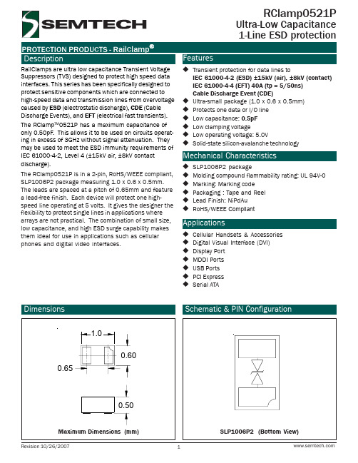
RCLAMP0522P中文资料
Applications
High Definition Multi-Media Interface (HDMI) Digital Visual Interface (DVI) Unified Display Interface (UDI) DisplayPortTM Interface MDDI Ports PCI Express Serial ATA
RClamp0522P RClamp0524P
PRELIMINARY
Power Derating Curve
110 100 90 80 70 60 50 40 30 20 10 0
PROTECTION PRODUCTS Typical Characteristics
Non-Repetitive Peak Pulse Power vs. Pulse Time
Pin 1
Pin 2
Pin 1
Pin 2
Pin 4
Pin 5
3, 4
3, 8
Circuit Diagram
Circuit Diagram
Ordering Information
Part Number RClamp0522P.TCT RClamp0524P.TCT Number of Lines Qty per Reel Reel Size 7 Inch 7 Inch
PRELIMINARY
RClamp0522P RClamp0524P
RClamp0524P
10 9 8 7 6
1
Pin 1-2 5-6 3-4
2
3
Identification Input Lines Output Lines (No Internal Connection) Ground Pin
REF02EP中文资料
General DescriptionThe REF01 and REF02 are precision voltage references that are pretrimmed to within ±3% of +10V and +5V,respectively. Both references feature excellent tempera-ture stability (as low as 8.5 ppm/°C worst case), low cur-rent drain, and low noise. The REF02 also provides a TEMP pin whose output voltage varies linearly with tem-perature, making this device suitable for a wide variety of temperature-sensing and control applications. Both devices are available from Maxim in the space-saving SO package, as well as in the standard 8-pin TO-99 and MINI-DIP packages.Featureso Pretrimmed to +5V, +10V ±0.3%o Excellent Temperature Stability: 3ppm/°C o Low Noise: 10µVp-p (REF02)o Low Supply Current: 1.4mA max o Short-Circuit Proofo Linear Temperature Transducer O/P (REF02)REF01/REF02+5V , +10V Precision Voltage References________________________________________________________________Maxim Integrated Products1__________Typical Operating Circuit19-0887; Rev 1; 8/99For free samples & the latest literature: , or phone 1-800-998-8800.For small orders, phone 1-800-835-8769.Ordering Information continued at end of data sheet.ApplicationsA to D Converters D to A Converters Digital Voltmeters Voltage Regulators Threshold DetectorsOrdering InformationReference with Trimmed OutputR E F 01/R E F 02+5V , +10V Precision Voltage References 2_______________________________________________________________________________________ABSOLUTE MAXIMUM RATINGS—REF01Stresses beyond those listed under “Absolute Maximum Ratings” may cause permanent damage to the device. These are stress ratings only, and functional operation of the device at these or any other conditions beyond those indicated in the operational sections of the specifications is not implied. Exposure to absolute maximum rating conditions for extended periods may affect device reliability.Input VoltageREF01, A, E, H, All DICE...................................................40V REF01C.............................................................................30V Power DissipationT099 (J) (derate at 7.1mW°C above 80°C).................500mW CERDIP (2) (derate at 6.7mW/°C above 75°C)...........500mW Plastic Dip (P) (derate at 5.6mW/°C above 36°C)......500mW Small Outline (S) (derate at 5.0mW/°C above 55°C)..300mW Output Short-Circuit Duration(to ground or V IN ).....................................................IndefiniteStorage Temperature Range.............................-65°C to +150°C Operating Temperature RangeREF01A, REF01............................................-55°C to +125°C REF01E, REF01H, REF01C(except REF01CESA) ..................................0°C to +70°C REF01CESA....................................................-40°C to +85°C DICE Junction Temperature (T j )........................-65°C to +150°C Lead Temperature (soldering, 60s).................................+300°CELECTRICAL CHARACTERISTICS—REF01(V IN = +15V, T A = +25°C, unless otherwise noted.)ELECTRICAL CHARACTERISTICS—REF01(V IN = +15V, -55°C ≤ T A = +125°C for REF01A and REF01, 0°C ≤T A ≤+70°C for REF01E and REF01H, I L = 0mA, unless otherwise noted.)Output AdjustmentThe REF01 trim terminal can be used to adjust the volt-age over a 10V±300mV range. This feature allows the system designer to trim system errors by setting the ref-erence to a voltage other than 10V, including 10.240V for binary applications (see the Typic al Operating Circuit section).Adjustment of the output does not significantly affect the temperature performance of the device. The tem-perature coefficient change is approximately 0.7ppm/°C for 100mV of output adjustment.REF01/REF02+5V , +10V Precision Voltage References_______________________________________________________________________________________3ELECTRICAL CHARACTERISTICS—REF01(V IN = +15V, T A = T MIN to T MAX , unless otherwise noted.)ELECTRICAL CHARACTERISTICS—REF01 (continued)(V IN = +15V, T A = +25°C, unless otherwise noted.)R E F 01/R E F 02+5V , +10V Precision Voltage References 4_______________________________________________________________________________________ABSOLUTE MAXIMUM RATINGS—REF02Input VoltageREF02, A, E, H, All DICE...................................................40V REF02C, D..........................................................................30V Power DissipationT099 (J) (Derate at 7.1mW°C above 80°C).................500mW CERDIP (2) (Derate at 6.7mW°C above 75°C)...........500mW Plastic Dip (P) (Derate at 5.6mW°C above 36°C).......500mW Small Outline (S) (Derate at 5.0mW°C above 55°C)...300mW Storage Temperature Range.............................-65°C to +150°COperating Temperature RangeREF02A, REF02............................................-55°C to +125°C REF02E, REF02H (Except REF02CESA) ........0°C to +70°C REF02C (except REF02CESA), REF02D...........0°C to +70°C REF02CESA........................................................-40°C to +85°C Lead Temperature (Soldering, 60s).................................+300°C DICE Junction Temperature (T j )........................-65°C to +150°C Output Short-Circuit Duration(to Ground or V IN ).....................................................IndefiniteELECTRICAL CHARACTERISTICS—REF01(V IN = +15V, -55°C ≤T A = +125°C for REF02A and REF02, 0°C ≤T A ≤+70°C for REF02E and REF02H, I L = 0mA, unless otherwise noted.)Stresses beyond those listed under “Absolute Maximum Ratings” may cause permanent damage to the device. These are stress ratings only, and functional operation of the device at these or any other conditions beyond those indicated in the operational sections of the specifications is not implied. Exposure to absolute maximum rating conditions for extended periods may affect device reliability.ELECTRICAL CHARACTERISTICS—REF02(V IN = +15V, T A = +25°C, unless otherwise noted.)Output AdjustmentThe REF02 trim terminal can be used to adjust the out-put voltage over a 5V±300mV range. This feature allows the system designer to trim system errors by set-ting the reference to a voltage other than 5V (refer to the Typical Operating Circuit section).Adjustment of the output does not significantly affect the temperature performance of the device. Typically,the temperature coefficient change is 0.7ppm/°C for 100mV of output adjustment.Temperature Voltage OutputThe REF02 provides a temperature-dependent output voltage on the TEMP pin. This voltage is proportional to the absolute temperature, and has a scale factor of approximately 2.1mV/°C (Figure 2).Output Voltage = 2.1(T + 273)mV where T = Temperature in °CREF01/REF02+5V, +10V Precision Voltage References_______________________________________________________________________________________5Figure 2. REF02 Temperature/Voltage Output vs. TemperatureELECTRICAL CHARACTERISTICS—REF02(V IN = +15V, T A = T MIN to T MAX and I L = 0mA, unless otherwise noted.)ELECTRICAL CHARACTERISTICS—REF02(V IN = +15V, T A = +25°C, unless otherwise noted.)R E F 01/R E F 02+5V , +10V Precision Voltage References 6_______________________________________________________________________________________Typical Operating CharacteristicsTypical ApplicationsChip TopographyREF01/REF02+5V , +10V Precision Voltage References_______________________________________________________________________________________7Figure 3. Precision Calibration StandardFigure 5. Current SourceFigure 4. ±10V ReferenceFigure 6. Precision Temperature Transducer withRemote SensorR E F 01/R E F 02+5V , +10V Precision Voltage References Ordering Information (continued)Pin ConfigurationMaxim c annot assume responsibility for use of any c irc uitry other than c irc uitry entirely embodied in a Maxim produc t. No c irc uit patent lic enses are implied. Maxim reserves the right to change the circuitry and specifications without notice at any time.8_____________________Maxim Integrated Products, 120 San Gabriel Drive, Sunnyvale, CA 94086 408-737-7600©1999 Maxim Integrated ProductsPrinted USAis a registered trademark of Maxim Integrated Products.*Contact factory for availability.*NOTE:Pin 3 is N.C. (No Connection) on REF01, TEMP Output on REF02.。
HNC-050P资料

Electrical dataPrimary nominal Primary current TypeDC current measuring range IPN(A)I P(A)500 .. ± 75HNC - 050P 1000 .. ± 140HNC - 100PHNC - 050P HNC - 100PR M Measuing resistance 60 .. 9060 .. 80ΩI SN Second nominal current 5050mA K N Turns ratio 1 : 1000 1 : 2000V C Supply voltage (± 5 %) ± 15V I C Current consumpution 15 + I SN mA V dR.m.s. voltage for AC isolation test, 50/60Hz, 1 min 2.5kVAccuracy-Dynamic performance dataXAccuracy @ T A = 25°C ± 1% of I PNεLLinearity (0 .. ± I PN )< ± 0.5%I O Electrical offset current @I P = 0, @T A = 25°C ± 0.2mA I HC Hysteresis offset current @ I P = 0,after an excursion of I PN ± 0.15mA I OT Thermal drift of I O 0°C .. +70°C ± 0.005ms/°C t rResponse time @ 90% of I P <1 µs TC εGThermal drift of the gain (% of reading) < ± 0.004%/°CGeneral dataT A Ambient operating temperature - 10 .. + 80°C T S Ambient storage temperature- 15 .. + 85°CHNC - 200PHNC - 300PR S Secondary coil Resistance@T A = 25°C 7595ΩmMass30gCurrent Transducer HNC- 050 .. 100PFor the electronic measurement of currents: DC, AC, pulsed, mixed,with a galvanic isolation between the primary circuit (high power) and the secondary circuit (electronic circuit).I PN = 50 .. 100 AFeatures• Hall effect measuring principle• Galvanic isolation between primaryand secondary circuit • Isolation voltage 2500 V • Low power consumptionAdvantages• Easy mounting• Small size and space saving • Only one design for wide currentratings range•High immunity to external interferenceApplications• DC motor drives• Switched Mode Power Supplies(SMPS)• AC variable speed drives• Uninterruptible Power Supplies (UPS)• Battery supplied applications • Inverterswww.nanalem.co.jp010301/1HNC- 050 .. 100PNANALEM reserves the right to carry out modifications on its transducers, in order to improve them, without previous notice.UNIT: mm。
S20P05资料]IEDM2011论文集
![S20P05资料]IEDM2011论文集](https://img.taocdn.com/s3/m/a99e017c571252d380eb6294dd88d0d233d43cdc.png)
Switchable Wide Tuning Range Bandstop Filters for Frequency-Agile Radios Zhengzheng Wu, Yonghyun Shim, and Mina Rais-ZadehDepartment of Electrical Engineering & Computer Science, University of Michigan, Ann Arbor, MI 48109, USAAbstractThis paper reports on micromachined tunable bandstop filters that exhibit an octave frequency tuning range with high stopband rejection and low out-of-band loss. In addition to continuous frequency tuning, stopband switch on-off capability is realized by employing ohmic switches along with tunable capacitors. The fully re-configurable filters in this work are fabricated using a silicon-based integrated passive device technology and are the smallest-size bandstop filters reported in the low SHF range.IntroductionReconfigurable and cognitive radios require frequency-agile RF front-end modules to cover a wide range of wireless spectrum. Tunable filters are imperative components of cognitive radios and have been the focus of much research in the past [1], [2]. In the presence of strong out-of-band interferers, pre-select RF filters can protect the receiver from gain desensitization, and the receiver linearity requirement is significantly relaxed. Filters with high rejection provide Tx/Rx isolation and are needed in frequency-division duplexing (FDD) transceivers and transmitter spurious emission control. Compared to bandpass filters, bandstop filters exhibit lower passband insertion loss, minimizing the degradation of receiver noise figure, while providing high rejection level for removing spurious signals. Therefore, tunable bandstop filters have the potential to replace more complicated and higher loss switched bandpass filter banks used in multi-band RF front-ends. In this paper, we report on a switchable wide tuning range bandstop filter. Filters are realized in a silicon-based integrated passive device (IP D) technology intended for multi-chip module integration.IPD Fabrication ProcessThe silicon-based IP D technology developed in this work offers both high-Q fixed RF passive components and tunable RF micro-electromechanical systems (MEMS) [3]. Fig. 1 shows the fabrication process steps. It offers three metal layers, one dielectric layer and a sacrificial layer. The process starts with passivating the substrate which is high resistivity (>1 k·cm) silicon. The bottom metal is deposited and patterned. The sacrificial layer is then deposited and step etched to allow the formation of dual air-gaps (as shown in Fig. 1(d)) for realizing high analog tuning range (>5:1) MEMS capacitors, and contact dimples used in MEMS ohmic switches. An electroplated gold layer is utilized as the structural layer for RF MEMS devices, and a thick electroplated copper layer is utilized for forming high-Q inductive components and low-loss transmission lines. The sacrificial layer is removed to release the tunable capacitors and RF switches. Finally, silicon is selectively removed under inductive components to reduce the substrate loss.Fig. 1. Fabrication process flow of the IPD. (a): Deposit oxynitride dielectric as surface passivation layer and evaporate bottom metal layer; (b): Deposit and pattern dielectric layer for MIM capacitors; (c): Deposit a sacrificial layer; (d): Step etch the sacrificial layer; (e): Electroplate 2nd metal layer for MIM capacitors and RF MEMS structural layer; (f): Electroplate thick metal for high-Q inductors; (g): Sacrificial layer removal and substrate micromachining to create air-suspended inductors.Tunable Bandstop FiltersThe design of tunable bandstop filter is based on coupled transmission line configuration, as shown in Fig. 2. The transmission line is loaded with a capacitor for reduced electrical length. A pair of lumped coupled inductors (layout shown in Fig. 2) is used to imitate the coupled transmission lines in the band of interest. The advantage of using lumped components over transmission lines is that they occupy a smaller area. Using this filter design, narrow bandwidth bandstop filters with performances superior to conventional LC type filters can be implemented using low-value and high-Q inductors. Wide tuning range MEMS capacitors are employed to tune the filter center frequency. As shown in Fig. 3, a fabricated MEMS capacitor can be tuned from 0.38 pF to 2.1 pF with applying a voltage of up to 35 V, demonstrating a tuning range of 5.5:1. The MEMS capacitor is modeled considering the resistive (Rseries) and inductive parasitic (Lseries), as shown in Fig. 4. Recalling from Fig. 2, the capacitor is connected in series with an inductor to form the resonator tank in the bandstop filter. The parasitic inductance of the capacitor (Lseries) is absorbed into the main inductor of the tank. Therefore, the overall Q of the LC tank is improved and its usable frequency range is extended.20.5.1IEDM11-493 978-1-4577-0505-2/11/$26.00 ©2011 IEEE123Fig. 2. Circuit implementation of the bandstop filterlumped coupled inductor pair.Fig. 3. Measured tuning range of a fabricated MEMS caFig. 4. Circuit model of the RF MEMS capacitor.A two-pole tunable bandstop filter is realiztwo 1st-order bandstop filter cells. Fig. 5 showof a fabricated two-pole tunable bandstop fithe filter is 2.2 mm × 2.6 mm. The measureof the bandstop filter are plotted in Fig.frequency is tuned from 6.5 GHz to 3.1more than an octave frequency coverage. Atuning range, the insertion loss at both lopassbands is measured to be less than 1 dB.0510*******0.30.60.91.21.51.82.1Capacitance(pF)Bias Voltage (V)4r and layout of theapacitor.zed by cascadingws a SEM imageilter. The size ofed tuning results. 6. The centerGHz, achievingAcross the entireower and higherThe filter shapeshows significant improvementreported lumped LC filter impleme[6]. The stopband rejection level isfrequency range of 5−6.5 GHz. Afrequencies, the filter bandwidcapacitance of the tank is incrbandwidth reduction and also thefrequencies, the filter rejectionfrequencies below 5 GHz.Fig. 5. A SEM image of a tunable bandstopFig. 6. Measured frequency response of thbias voltage shown). (a) Insertion loss; (b) reThe linearity of the tunable bandsusing a two-tone test. A two-frequency of 5.25 GHz and inpuapplied to the bandstop filter when5.25 GHz. Figs. 7(a) and (b) showan input frequency offset of 1 kHz30350246-35-30-25-20-15-10-5InsertionLoss(dB)Frequency (G0246-40-30-20-100V5V9V11V13V14V15V16V17V18V29VReturnLoss(dB)Frequency (Gcompared with otherentations in this range [4]–s better than 20 dB in theAt lower stopband centerdth is reduced as thereased. Because of thislower inductor Q at lown level is degraded atfilter.he tunable bandstop filter (witheturn loss.stop filter is characterized-tone input with centerut power of -10 dBm isn the stopband is tuned tothe output spectrum withand 1 MHz, respectively.810120V5V9V11V13V14V15V16V17V18V29VGHz)81012GHz)20.5.2IEDM11-494The extracted 3rd–order input intercept point (IIP3) from the measurement is 3.6 dBm at 1 kHz frequency offset, as is shown in Fig. 8. At a higher two-tone frequency offset the 3rd-order inter-modulation output signals are below the noise floor, and the IIP3 cannot be extracted. This is because the MEMS capacitor has a lowpass response [1] that filters out the inter-modulation products with offset frequencies higher than the mechanical resonance frequency of the movable membrane. Therefore, inter-modulation products are highly attenuated if they fall in the lower and higher passbands of the bandstop filter, showing benefit of using MEMS devices as part of a filter.Fig. 7. Measured output spectrum with a two-tone test at 5.25 GHz and -10 dBm input power; (a) 1 kHz offset, and (b) 1 MHz offset.O u t p u t P o w e r (d B m )Input Power (dBm)Fig. 8. Extraction of IIP3 with a two-tone input frequency offset of 1 kHz.The tuning speed of the bandstop filter is measured by applying a step-function actuation bias to the MEMS capacitors. The measured tuning speed of the tunable bandstop filter is better than 80 μs as shown in Fig. 9.A p p l i e d Vo l t a g e (V )Time (μs)D e t e c t e d V o l t a g e (V )Fig. 9. Measured tuning speed of the tunable bandstop filter. The tuning speed is better than 80 µs.Switchable Bandstop FiltersIn a cognitive spectrum utilization scheme, it is useful to switch off the bandstop filter in case no interference is present. When the filter is switched off, additional channel loss introduced by the filter will be minimized and the available wireless spectrum will be fully utilized. In this work, a MEMS ohmic switch is exploited to add switch on/off capability to the wide tuning range bandstop filters. As shown in the circuit schematic of Fig. 10, a MEMS ohmic switch is connected in parallel with the tunable capacitor. When the RF MEMS ohmic switch is in contact, it shorts the capacitive load port to the ground. In this switched-off state, the filter becomes an all-pass network.Fig. 10. Circuit model of the tunable bandstop filter with switch on/off capability and the electrical model of the MEMS ohmic switch.In the proposed switchable bandstop filter design, the MEMS switch is placed in the coupled line section instead of in the main RF signal path (Fig. 10). Therefore, the filter loss is less sensitive to the contact resistance of the ohmic switch. The pass-band insertion loss of the filter having different contact resistance (R contact ) for the switch is simulated and shown in Fig. 11. Simulation results indicate that even with a contact resistance of 10Ω, the insertion loss is less than 0.83 dB up to 10 GHz. Because of the low sensitivity to contact resistance, the switchable filter can also employ RF MEMS switches that use hard metals (e.g. Ru) as the contact material. Such switches offer good reliability [7].Fig. 11. Insertion loss of the filter path when the bandstop filter is switched off using a MEMS ohmic switch.(a)(b)-4-224-120-80-400O u t p u t P o w e r (d B m )Frequency Offset (kHz)-4-224-120-80-40Frequency Offset (MHz)I n s e r t i o n L o s s (d B )Frequency (GHz)20.5.3IEDM11-495A SEM image of a fabricated switchable filter is shown in Fig. 12. The RF MEMS ohmic switch is embedded in the capacitive load port, as can be seen in the close-up view show in Fig. 12. The size of the switchable filter is 2.2 mm × 2.6 mm, similar to the size of the tunable bandstop filter. The measured response of the filtering path when the bandstop filter is switched off is shown in Fig. 13. With increasing actuation voltage on the switch, the contact resistance of the RF MEMS switch is reduced and the insertion loss of the switched-off bandstop filter is improved. The measured insertion loss is less than 0.84 dB up to 10 GHz. The higher insertion loss in measured results is due to the higher resistance of the electroplated metal and fabrication imperfections that cause non-ideal electrical performance for the lumped coupled inductors. The bandstop filter responses at switch on/off states are compared in Fig. 14.Fig. 12. A SEM image of the fabricated tunable bandstop filter with closed-up view and circuit model of the RF MEMS ohmic switch (up-state).I n s e r t i o n L o s s (d B )Frequency (GHz)6R e t u r n L o s s (d B )Frequency (GHz)Fig. 13. Measured responses of the switched-off bandstop filter with varied DC bias on MEMS ohmic switch; (a) Insertion loss, and (b) return loss.I n s e r t i o n L o s s (d B )Frequency (GHz)R e t u r n L o s s (d B )Fig. 14. Insertion loss and return loss when the bandstop filter is switched-on and switched-off (a 30 V bias on ohmic switch).ConclusionIn this paper, wide tuning range miniaturized bandstop filters are implemented. These tunable filters provide high interference rejection capability and low passband insertion loss. A stopband switch on-off technique is proposed which is tolerant to contact resistance of ohmic switches. Filters are fabricated using a silicon-based IP D technology which can be used to realize other miniaturized frequency-agile RF front-ends.AcknowledgementThe authors would like to acknowledge the staff of the Lurie Nanofabrication Facility at the University of Michigan for their assistance with fabrication. This work is supported by National Science Foundation under award number1055308.References[1] G.M. Rebeiz, et al., "Tuning in to RF MEMS," IEEE Microw. Mag.,vol. 10, no. 6, pp. 55-72, Oct. 2009.[2] H.A.C. Tilmans, W. De Raedt, and E. Beyne, "MEMS for wirelesscommunications: 'from RF-MEMS components to RF-MEMS-SiP'," Journal of Micromechanics and Microengineering , vol. 13, pp. S139-163, July 2003.[3] Z. Wu, Y. Shim, and M. Rais-Zadeh, "Miniaturized UWB bandpassfilters integrated with notch filters using a silicon-based integrated passive device technology," 2011 IEEE MTT-S International Microwave Symposium , June 2011.[4] M. Fernandez-Bolaos, T. Lisec, C. Dehollain, D. Tsamados, P. Nicole,and A.M. Ionescu, "Highly tunable band-stop filters based on AlN RF MEM capacitive switches with inductive arms and zipping capacitive coupling," 2009 IEEE International Electron Devices Meeting , Dec. 2009.[5] P. Ekkels, et al., "Air gap-based MEMS switch technology usingnickel surface micromachining," Sensors and Actuators A: Physical , vol. 166, no. 2, pp. 256-263, Apr. 2011.[6] H.S. Lee, D.H. Choi, and J.B. Yoon, "MEMS-based tunable LCbandstop filter with an ultra-wide continuous tuning range," IEEE Microw. Wireless Compon. Lett., vol. 19, no. 11, pp. 710-712, Nov. 2009. [7] C.D. Patel and G.M. Rebeiz, "An RF-MEMS switch with mN contactforces," 2010 IEEE MTT-S International Microwave Symposium , May 2010.20.5.4IEDM11-496。
IOS-MAT-0054_CNv5
参考
本技术规范中化学品要求和测试所引用的标准,如欧盟指令,都适用标准、指令的最新版本,除非 另有说明。
本资料仅供参考,英文版本 IOS-MAT-0054 具有最终法律效力。
1 of 23 2009-10-26 Elsa Hou 译稿
表2. 实木、木基材料和天然材料的要求
物质
要求
测试方法
文件
硼及其化合物
不允许使用硼及其化合物。
在实木(包括实木拼板)、 污染限值:硼及其化合物的迁移 天然纤维、胶合板、层压 值:30 mg 硼/kg 板/弯曲木中
如果木材有涂层,在 SD 测试前应去除涂层。
DIN 53160(用人工 合成汗液进行萃取, 16小时,23 °C), 然后依照EN ISO 11885(ICP/AES分 析)
IOS-MAT-0054 第五版译文
原版本代号:
审稿人:Jason Liu, Teresa Xu, Sebrina Chen
AA-92520-5 2009-10-09
化合物和化学物质:对儿童产品与玩具的附加要求
内容
本规范阐述了宜家对所有儿童产品(包括玩具)的化合物和化学物质的附加要求。
关于此规范
本规范的目的是确保儿童产品和玩具在儿童使用时是安全的,因为儿童更为敏感,并且接触产品的 方式与成人不同(如吮吸和咀嚼)。
染料
不允许使用。
在印刷或上色的纸/纸板中 污染限值:每种染料10 mg/kg
甲醛(50-00-0)
甲醛含量不可高于30mg/kg。 EN 71-11
文件 SD
SD
2.3 纺织品
表4.对纺织品的要求
AC DC 电源模块 LDE03 05-20Bxx 系列 商品说明书

3W/5W ,AC-DC模块电源CB RoHS产品特点●全球通用电压:85-264VAC/100-370VDC ●工作温度范围:-40℃to +70℃●4000VAC 高隔离电压●稳压输出、低纹波噪声●输出短路、过流、过压保护●高效率、高可靠性●全塑料外壳,符合UL94V-0●EMI 性能满足CISPR32/EN55032CLASS B●符合IEC62368、UL62368、EN62368认证标准(认证中)LDE03/05-20Bxx 系列------是金升阳为客户提供的小体积开关模块电源。
该系列电源具有全球输入电压范围、交直流两用、低功耗、高效率、安全隔离等优点。
产品安全可靠。
该系列产品应用在电磁兼容比较恶劣的环境下时必须参考应用电路。
选型表认证型号输出功率标称输出电压及电流(Vo/Io)效率(230VAC/%,Typ.)最大容性负载(uF )UL/CE/CB (认证中)LDE03-20B03 2.3W3.3V/700mA 666000LDE03-20B053W5V/600mA 746000LDE03-20B099V/330mA 751500LDE03-20B1212V/250mA 771500LDE03-20B1515V/200mA 771000LDE03-20B2424V/125mA 78330LDE05-20B03 3.3W 3.3V/1000mA 685000LDE05-20B055W 5V/1000mA 755000LDE05-20B099V/560mA 771200LDE05-20B1212V/420mA 791200LDE05-20B1515V/330mA 791000LDE05-20B2424V/210mA81330输入特性项目工作条件Min.Typ.Max.单位输入电压范围交流输入85--264VAC 直流输入100--370VDC 输入频率47--63Hz输入电流LDE03115V AC ----80mA230V AC ----45LDE05115V AC ----130230V AC----70冲击电流115V AC --10--A230V AC--20--漏电流0.1mA RMS typ.230V AC/50Hz外接保险管推荐值1A/250V ,慢断,必接热插拔不支持项目工作条件Min.Typ.Max.单位输出电压精度 3.3V 输出--±3--%其它--±2--线性调节率满载--±0.5--负载调节率0%-100%负载--±1--输出纹波噪声*20MHz 带宽(峰-峰值)--50100mV 温漂系数--±0.02--%/℃短路保护打嗝式,可长期短路,自恢复过流保护LDE03≥150%Io 自恢复LDE05≥120%Io 自恢复过压保护3.3/5VDC 输出≤7.5VDC 9VDC 输出≤15VDC 12/15VDC 输出≤20VDC 24VDC 输出≤30VDC最小负载0----%掉电保持时间LDE03115V AC 输入--10--ms 230V AC 输入--60--LDE05115V AC 输入--5--230V AC 输入--50--注:*纹波和噪声的测试方法采用平行线测试法,具体操作方法参见《AC-DC 模块电源应用指南》。
RCLAMP0521P中文资料
Typical 9.3
Maximum 5 11
Units V V
0.025
1
µA
15
V
25
V
0.30
0.50
pF
2007 Semtech Corp.
2
元器件交易网
RClamp0521P
Clamping Voltage - VC (V)
PROTECTION PRODUCTS Typical Characteristics
Mechanical Characteristics
SLP1006P2 package Molding compound flammability rating: UL 94V-0 Marking: Marking code Packaging : Tape and Reel Lead Finish: NiPdAu RoHS/WEEE Compliant
90 80 70 60 50 40 30 20 10
0 0
Power Derating Curve
25
50
75
100
125
150
Ambient Temperature - TA (oC)
Clamping Voltage vs. Peak Pulse Current
24 22 20 18 16 14 12 10
10 MHz
100 MHz
13 GHz GHz
START. 030 MHz
STOP 3000.000000 MHz
3
元器件交易网
PROTECTION PRODUCTS Applications Information
PFKC05-24S15中文资料
PFKC05-24S15中文资料OUTPUT SPECIFICATIONSOutput power5 Watts maxVoltage accuracy Full load and nominal Vin ± 2%Minimum load (Note 1)10% of FL Line regulation LL to HL at Full Load ± 0.2%Load regulation25% to 100% FL Single Dual ± 0.5%± 2%Cross regulation (Dual) Asymmetrical load 25% / 100% FL ± 5%Ripple and noise 20MHz bandwidth 3.3V/5V others 75mVp-p1%/p-p of Vout maxTemperature coefficient I 0.02% / oC, maxTransient response recovery time 25% load step change500uS Over load protection % of FL at nominal input180% typShort circuit protectionContinuous, automatics recoveryINPUT SPECIFICATIONSInput voltage range 12V nominal input 24V nominal input 48V nominal input 9 – 18VDC 18 – 36VDC 36 – 75VDC Input filter Pi type Input surge voltage 100mS max 12V input 24V input 48V input36VDC50VDC 100VDCInput reflected ripple Nominal Vin and full load150mAp-p Start up timeNominal Vin and constant resistor load30mS typGENERAL SPECIFICATIONSEfficiency See table Isolation voltage Input to OutputStandard Suffix -H1600VDC, min3000VDC, min Isolation resistance 109ohms, min Isolation capacitance 300pF, max Switching frequency 100KHz, minApprovals and standard IEC60950, UL1950, EN60950Case material Non-conductive black plastic Base material Non-conductive black plasticPotting material Epoxy (UL94-V0)Dimensions 1.25 X 0.80 X 0.40 Inch (31.8 X 20.3 X 10.2 mm) Weight DIP SMD14g (0.48oz)15g (0.52oz)MTBF (Note 2)3.731 x 10⁶hrsENVIRONMENTAL SPECIFICATIONSOperating temperature range-25oC ~ +71oC Storage temperature range-55oC ~ +105oC Thermal shock MIL-STD-810DVibration 10~55Hz, 2G, 30minutes along X,Y and ZRelative humidity5% to 95% RHEMC CHARACTERISTICSConducted emissions EN55022 Level A Radiated emissions EN55022 Level AESD EN61000-4-2 Perf. Criteria2Radiated immunityEN61000-4-3 Perf. Criteria2Fast transientEN61000-4-4Perf. Criteria2Surge EN61000-4-5 Perf. Criteria2Conducted immunityEN61000-4-6Perf. Criteria2The PFKC05 series offer 5 watts of output power from a package in an IC compatible 24pin DIP configuration without derating to 71oC ambient temperature and pin to pin compatible with PFKC03, FKC03, FKC05 series. PFKC05 series have 2:1 wide input voltage of 9-18, 18-36 and 36-75VDC. The PFKC05 features 1600VDC of isolation and, short-circuitprotection and suffix “ H ” can get 3000VDC isolation. All models are particularly suited to telecommunications, industrial, mobile telecom and test equipment applications.TE C H N I C A L S P E C IF I C A T I O N All specifications are typical at nominal input,full load and 25oC otherwise noted UL E193009TUV R50008270CB JPTUV-003680 CE MARK5 WATTS REGULATED OUTPUT POWER ? 2:1 WIDE INPUT VOLTAGE RANGEINTERNATIONAL SAFETY STANDARD APPROVAL ? OVER CURRENT PROTECTION ? HIGH EFFICIENCY UP TO 80% STANDARD 24 PIN DIP PACKAGE & SMD TYPE PACKAGE50 60 7080 90 100-40 -25 0-10 AMBIENT TEMPERATURE (oC)O U T P U T P O W E R (%)PFKC05-48S05 Derating CurveModel NumberInput RangeOutput VoltageOutput CurrentInputCurrent (3)Eff (4)(%)Capacitor (5)Load maxPFKC05-12S339 – 18 VDC 3.3 VDC 1000mA 404mA 72 2200uFPFKC05-12S05 9 – 18 VDC 5 VDC 1000mA 579mA 76 1000uF PFKC05-12S129 – 18 VDC 12 VDC 470mA 618mA 80 220uF PFKC05-12S15 9 – 18 VDC 15 VDC 400mA 658mA 80 150uF PFKC05-12D05 9 –18 VDC ± 5 VDC ± 500mA 571mA 77± 680uF PFKC05-12D12 9 –18 VDC ± 12 VDC ± 230mA 605mA 80 ± 100uF PFKC05-12D15 9 –18 VDC ± 15 VDC ± 190mA 625mA 80 ± 68uF PFKC05-24S33 18 – 36 VDC 3.3 VDC1000mA 202mA 722200uF PFKC05-24S05 18 – 36 VDC 5 VDC 1000mA 278mA 79 1000uF PFKC05-24S12 18 – 36 VDC 12 VDC 470mA 306mA 81 220uF PFKC05-24S15 18 –36 VDC 15 VDC 400mA 325mA 81 150uF PFKC05-24D05 18 –36 VDC ± 5 VDC ± 500mA 282mA 78 ± 680uF PFKC05-24D12 18 –36 VDC ± 12 VDC ± 230mA 299mA 81 ± 100uF PFKC05-24D15 18 –36 VDC ± 15 VDC ± 190mA 309mA 81 ± 68uF PFKC05-48S33 36 – 75 VDC 3.3 VDC 1000mA 100mA 73 2200uF PFKC05-48S05 36 –75 VDC 5 VDC 1000mA 141mA 78 1000uF PFKC05-48S12 36 – 75 VDC 12 VDC 470mA 153mA 81 220uF PFKC05-48S15 36 –75 VDC 15 VDC 400mA 162mA 81 150uF PFKC05-48D05 36 –75 VDC ± 5 VDC ± 500mA 143mA 77 ± 680uF PFKC05-48D12 36 –75 VDC ± 12 VDC ± 230mA 149mA 81 ± 100uF PFKC05-48D1536 – 75 VDC± 15 VDC± 190mA154mA81 ± 68uF2. Pin pitch tolerance I 0.014(0.35)Pin size is 0.02(0.5) Dia or 0.01 x 0.02 (0.25 x 0.50) Rectangular Pin Note1. The PFKC05 series required a minimum 10% loading on the output to maintain specified regulation. Operation under no-load condition will not damage these devices, however they may not meet all listed specification2. BELLCORE TR-NWT-000332. Case I: 50% Stress, Temperature at 40oC. (Ground fixed and controlled environment)3. Maximum value at nominal input voltage and full load of standard type.4. Typical value at nominal input voltage and full load.5. Test by minimum Vin and constant resistor load. Suffix-SMD。
负温度系数热敏电阻器:TTC05 系列
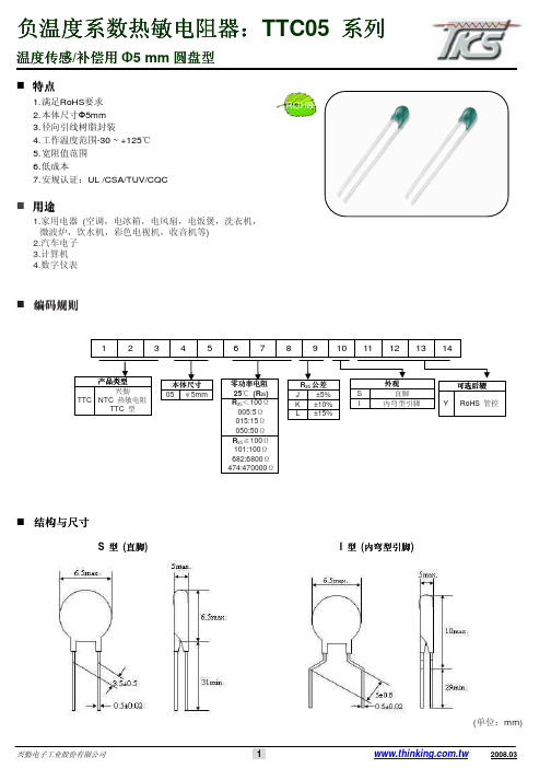
0.1 -30 -20 -10 0 10 20 30 40 50 60 70 80 90 100 110 120 130
温度 (℃)
A
Max ±0.5 Max.
(单位:mm)
D0
t
±0.2 ±0.2
12 9
3 18 1
4 0.6
12 9
3 18 1
4 0.6
■ 包装数量
散装: 200 pcs/袋 卷轴包装: 2500 pcs/卷
盒装: 2000 pcs/盒
兴勤电子工业股份有限公司
(单位:mm)
(单位:mm) 7
W
L
348mm 275mm
■电气特性
型号
零功率电阻 @25°C
R25 公差
TTC05005□ TTC05010□ TTC05015□ TTC05020□ TTC05025□ TTC05045□ TTC05050□ TTC05060□ TTC05085□ TTC05090□ TTC05101□ TTC05121□ TTC05151□ TTC05201□ TTC05221□ TTC05251□ TTC05301□ TTC05471□ TTC05501□ TTC05681□ TTC05701□ TTC05102□ TTC05152□ TTC05202□ TTC05222□ TTC05252□ TTC05302□ TTC05332□ TTC05402□ TTC05472□ TTC05502□ TTC05602□ TTC05682□ TTC05802□ TTC05103□ TTC05123□ TTC05153□ TTC05203□ TTC05303□ TTC05473□ TTC05503□ TTC05104□ TTC05154□ TTC05204□ TTC05224□ TTC05474□
- 1、下载文档前请自行甄别文档内容的完整性,平台不提供额外的编辑、内容补充、找答案等附加服务。
- 2、"仅部分预览"的文档,不可在线预览部分如存在完整性等问题,可反馈申请退款(可完整预览的文档不适用该条件!)。
- 3、如文档侵犯您的权益,请联系客服反馈,我们会尽快为您处理(人工客服工作时间:9:00-18:30)。
r
celduc
e l a i
s
元器件交易网
I/SEC/AC05-001/F/17/06/2008
page 2 / 6 F/GB
Temps de commutation Méthode de mesure / Test process ---> Alimentation de bobine /Coil voltage: ATF + 50% à l'action ( rebonds inclus ) / Operate time ( bounces included ) 1 ms au relâchement / Release time 0,4 ms CARACTERISTIQUES PHYSIQUES / PHYSICAL DATAS Matériau utilisé pour le contact / Contact material Sorties dorées, non étamées / Gold plated leads ( no tinned ) Température maxi d'utilisation / Max. operating temperature Température de stockage / Storage temperature Chocs ( 1/2 onde - 11 ms ) / Shocks ( 1/2 sine wave - 11 ms ) Vibrations ( de 30 à 2300 Hz ) / Vibrations Durée de vie mécanique / Mecanical life expextancy CARACTERISTIQUES MAGNETIQUES / MAGNETICAL DATAS Bobine de test / Test coil : R = 870 Ω "ST3" Nombre de spires / turns : 5 000 Référence ( Plage standard d'Ampères Tours de fermeture ) / Reference ( standard pull-in value ) Ruthénium - 60 à + 155°C - 70 à + 155°C 30 g 20 g 109
+ 0,5 3,1 0
元器件交易网
I/SEC/AC05-001/F/17/06/2008
page 4 / 6 F/GB
CAMBRAGE SPECIAUX / SPECIFIC BENDING
AC05P030 20 ≤ AT ≤ 25
20,87 ± 0,2 ( 3,33 ) = 14,2 max ( 3,33 ) = Ø 2,3 max
celduc
r e l a i s
Rue Ampère B.P. 4 42290 SORBIERS - FRANCE E-Mail : celduc-relais@ Fax +33 (0) 4 77 53 85 51 Service Commercial France Tél. : +33 (0) 4 77 53 90 20 Sales Dept.For Europe Tel. : +33 (0) 4 77 53 90 21 Sales Dept. Asia : Tél. +33 (0) 4 77 53 90 19
mesure de tension voltage measurement
30 mm
1010 Ω 0,7 pF 400 Hz 7000 Hz
Proud to serve you
All technical caracteristics are subject to change without previous notice. Caractéristiques sujettes à modifications sans préavis.
元器件交易网
I/SEC/AC05-001/F/17/06/2008
page 6 / 6 F/GB
CAMBRAGE SPECIAUX / SPECIFIC BENDING
AC05P090 15 ≤ AT ≤ 20
26,55 ±0,25 (6,18) = 14,2 max (6,18) = Ø 2,3 max
元器件交易网
I/SEC/AC05-001/F/17/06/2008
page 1 / 6 F/GB
AC05 . . . .
INTERRUPTEUR REED REED SWITCH
NORMALEMENT OUVERT, CONTACT SEC NORMALY OPEN, DRY CONTACT
Différentiel :
ATO ATF
Drop out value Pull in value
D ≥ 0,5
Durée de vie ( charges résistives ) / Life expectancy
5 mV = ; 10 mA 24 V = ; 400 mA
> 1 . 108 > 1 . 105
DATAS 10 W / 12 VA 100 Vdc 0,5 A 0,7 A 220 Vdc 250 Vdc ≤ 100 mΩ
ATf ≤ 25 ATf > 25
Résistance de contact initiale ( max ) / Initial contact resistance Méthode de mesure / Test process Bobine / Coil : voir caractéristiques magnétiques see magnetical datas Mesure en 4 points / 4 points measurement I = 100 mA ; U = 12 V et / and I = 10 mA ; U = 50 mV Alimentation de bobine /Coil voltage: ATF + 50% Résistance d'isolement ( min ) / Insulation resistance Capacité / Capacitance Fréquence maxi d'utilisation / Max. operating frequency Fréquence de résonnance / Resonant frequency
celduc
r e l a i s
Rue Ampère B.P. 4 42290 SORBIERS - FRANCE E-Mail : celduc-relais@ Fax +33 (0) 4 77 53 85 51 Service Commercial France Tél. : +33 (0) 4 77 53 90 20 Sales Dept.For Europe Tel. : +33 (0) 4 77 53 90 21 Sales Dept. Asia : Tél. +33 (0) 4 77 53 90 19
AC051530 ( de 15 à 30 ATf / from 15 up to 30 AT )
Pour des applications particulières ( autres sensibilités, plage réduite, coupe, cambrage ), prière de nous consulter. For special applications ( others pull-in-range, reduced range, cutting out, bending ), please contact us.
3,6 ±02
Ø 0,55
celduc
r e l a i s
Rue Ampère B.P. 4 42290 SORBIERS - FRANCE E-Mail : celduc-relais@ Fax +33 (0) 4 77 53 85 51 Service Commercial France Tél. : +33 (0) 4 77 53 90 20 Sales Dept.For Europe Tel. : +33 (0) 4 77 53 90 21 Sales Dept. Asia : Tél. +33 (0) 4 77 53 90 19
entraxe 20,32 ± 0,3 Ø 0,55
AC05P040 10 ≤ AT ≤ 25
14,2 max 3,25 ( extérieur patte ) Ø 2,3 m
lames non coupées / contacts ends without cutting
+ 0,5 3,1 0
Ø
celduc
Ø 2,3 max
Ø 0,5 max 14,2 max 44,7 max
CARACTERISTIQUES ELECTRIQUES / ELECTRICAL Puissance maxi commutable / Max. switching power Tension maxi commutable / Max. switching voltage Courant maxi commutable / Max. switching current Courant de travail / Carrying current Tension typique de tenue / Typical dielectric strength
r e l a i s
Rue Ampère B.P. 4 42290 SORBIERS - FRANCE E-Mail : celduc-relais@ Fax +33 (0) 4 77 53 85 51 Service Commercial France Tél. : +33 (0) 4 77 53 90 20 Sales Dept.For Europe Tel. : +33 (0) 4 77 53 90 21 Sales Dept. Asia : Tél. +33 (0) 4 77 53 90 19