PD438C;中文规格书,Datasheet资料
AO4803A;中文规格书,Datasheet资料

THIS PRODUCT HAS BEEN DESIGNED AND QUALIFIED FOR THE CONSUMER MARKET. APPLICATIONS OR USES AS CRITICAL COMPONENTS IN LIFE SUPPORT DEVICES OR SYSTEMS ARE NOT AUTHORIZED. AOS DOES NOT ASSUME ANY LIABILITY ARISING OUT OF SUCH APPLICATIONS OR USES OF ITS PRODUCTS. AOS RESERVES THE RIGHT TO IMPROVE PRODUCT DESIGN, FUNCTIONS AND RELIABILITY WITHOUT NOTICE.
Gate-Source Voltage
VGS
Continuous Drain
TA=25°C
Current
TA=70°C
Pulsed Drain Current C
Avalanche Current C
Avalanche energy L=0.1mH C
ID
IDM IAS, IAR EAS, EAR
TA=25°C Power Dissipation B TA=70°C
PD
Junction and Storage Temperature Range
TJ, TSTG
Maximum -30 ±20 -5 -4 -30 17 14 2 1.3
IRG4PC40KPBF;中文规格书,Datasheet资料

VCC = 80%(VCES), VGE = 20V, L = 10µH, RG = 10Ω,
(See fig. 13a)
Pulse width ≤ 80µs; duty factor ≤ 0.1%. Pulse width 5.0µs, single shot.
2
TO-247AC
Max.
600 42 25 84 84 10 ±20 15 160 65 -55 to +150 300 (0.063 in. (1.6mm) from case) 10 lbfin (1.1Nm)
Units
V A
µs V mJ W
°C
Thermal Resistance
Parameter
Repetitive rating; VGE = 20V, pulse width limited by
max. junction temperature. ( See fig. 13b )
Repetitive rating; pulse width limited by maximum
junction temperature.
TC , Case Temperature ( ° C)
TJ , Junction Temperature ( ° C)
Fig. 4 - Maximum Collector Current vs. Case Temperature
Fig. 5 - Typical Collector-to-Emitter Voltage vs. Junction Temperature
Switching Characteristics @ TJ = 25°C (unless otherwise specified)
PT4243A;PT4244C;PT4242C;PT4243N;PT4244A;中文规格书,Datasheet资料
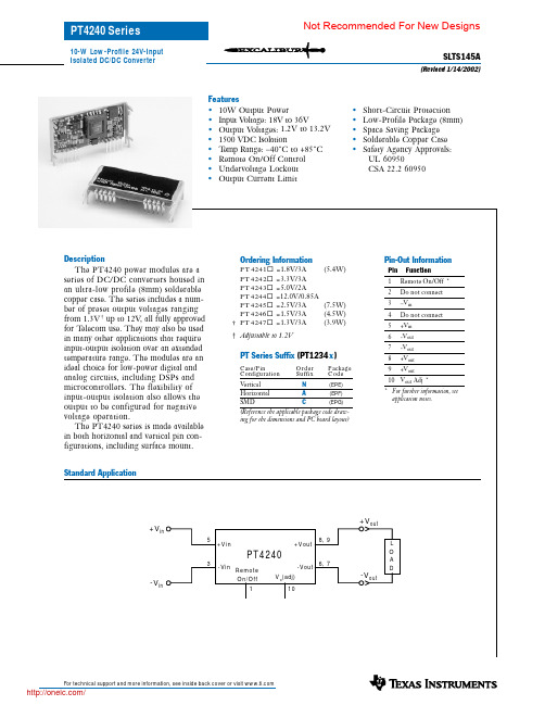
Standard Application
Ordering Information
Mechanical Shock
Mechanical Vibration
Weight Flammability
Io
Vin Vo tol Regtemp Regline Regload ∆Votot η
Vr
ttr ∆Vtr Vadj Ilim ƒs UVLO VIH VIL IIL Iin standby Cin Cout
PT Series Suffix (PT1234 x )
Case/Pin Configuration
Order Suffix
Package Code
Vertical Horizontal SMD
N
(EPE)
A
(EPF)
C
(EPG)
(Reference the applicable package code drawing for the dimensions and PC board layout)
Vo ≤ 5.0V Vo = 12V
Vo ≥2.5V
Vin =18V, ∆Vo = –1%
Over Vin range
Referenced to –Vin (pin 3)
pins 1 & 3 connected
Vo ≤ 5.0V Vo = 12V Input–output/input–case Input to output Input to output Over Vin range — Per Bellcore TR-332 50% stress, Ta =40°C, ground benign Per Mil-Std-883D, method 2002.3, 1mS, half-sine, mounted to a fixture Mil-Std-883D, Method 2007.2 20-2000Hz, all case styles soldered to PC — Materials meet UL 94V-0
AOD438中文资料

SymbolTyp Max 14.2203950R θJC 0.8 1.5Maximum Junction-to-AmbientASteady-State °C/W Maximum Junction-to-CaseCSteady-State°C/WThermal Characteristics ParameterUnits Maximum Junction-to-Ambient At ≤ 10s R θJA °C/W AOD438AOD438SymbolMin TypMaxUnits BV DSS 30V 1T J =55°C5I GSS 100nA V GS(th)1 1.83V I D(ON)85A 2.8 3.5T J =125°C4.45.54.4 5.5m Ωg FS 106S V SD 0.721V I S85A C iss 32003840pF C oss 590pF C rss 414pF R g0.540.7ΩQ g (10V)6376nC Q g (4.5V)3340nC Q gs 8.6nC Q gd 17.6nC t D(on)12ns t r 15.5ns t D(off)40ns t f 14ns t rr 3441ns Q rr30nCTHIS PRODUCT HAS BEEN DESIGNED AND QUALIFIED FOR THE CONSUMER MARKET. APPLICATIONS OR USES AS CRITICAL COMPONENTS IN LIFE SUPPORT DEVICES OR SYSTEMS ARE NOT AUTHORIZED. AOS DOES NOT ASSUME ANY LIABILITY ARISING OUT OF SUCH APPLICATIONS OR USES OF ITS PRODUCTS. AOS RESERVES THE RIGHT TO IMPROVE PRODUCT DESIGN,FUNCTIONS AND RELIABILITY WITHOUT NOTICE.Gate Drain Charge V GS =0V, V DS =15V, f=1MHz SWITCHING PARAMETERS Total Gate Charge Gate Source Charge Gate resistanceV GS =0V, V DS =0V, f=1MHzV GS =4.5V, V DS =15V, I D =20ATotal Gate Charge Turn-On Rise Time Turn-Off DelayTime V GS =10V, V DS =15V, R L =0.75Ω, R GEN =3ΩTurn-Off Fall TimeTurn-On DelayTime m ΩV GS =4.5V, I D =20AI S =1A,V GS =0VV DS =5V, I D =20AMaximum Body-Diode Continuous CurrentInput Capacitance Output CapacitanceDYNAMIC PARAMETERS R DS(ON)Static Drain-Source On-ResistanceForward TransconductanceDiode Forward Voltage I DSS µA Gate Threshold Voltage V DS =V GS I D =250µA V DS =24V, V GS =0VV DS =0V, V GS = ±20V Zero Gate Voltage Drain Current Gate-Body leakage current Electrical Characteristics (T J =25°C unless otherwise noted)STATIC PARAMETERS Parameter Conditions Body Diode Reverse Recovery TimeBody Diode Reverse Recovery Charge I F =20A, dI/dt=100A/µsDrain-Source Breakdown Voltage On state drain currentI D =250µA, V GS =0V V GS =10V, V DS =5V V GS =10V, I D =20AReverse Transfer Capacitance I F =20A, dI/dt=100A/µsA: The value of R θJA is measured with the device mounted on 1in 2 FR-4 board with 2oz. Copper, in a still air environment with T A =25°C. The Power dissipation P DSM is based on steady-state R θJA and the maximum allowed junction temperature of 150°C. The value in any givenapplication depends on the user's specific board design, and the maximum temperature of 175°C may be used if the PCB or heatsink allows it.B. The power dissipation P D is based on T J(MAX)=175°C, using junction-to-case thermal resistance, and is more useful in setting the upperdissipation limit for cases where additional heatsinking is used. It is used to determine the current rating, when this rating falls below the package limit.C: Repetitive rating, pulse width limited by junction temperature T J(MAX)=175°C.D. The R θJA is the sum of the thermal impedence from junction to case R θJC and case to ambient.E. The static characteristics in Figures 1 to 6 are obtained using <300 µs pulses, duty cycle 0.5% max.F. These tests are performed with the device mounted on 1 in 2 FR-4 board with 2oz. Copper, in a still air environment with T A =25°C. The SOA curve provides a single pulse rating.G. The maximum current rating is limited by the package current capability. Rev 2: July 2005AOD438AOD438AOD438。
BY459X-1500,127;BY459X-1500S,127;中文规格书,Datasheet资料
T
t
10us 100us 1ms 10ms 100ms 1s 10s
pulse width, tp (s)
BY459F
Fig.7. Transient thermal impedance Zth = f(tp)
Product specification
BY459X-1500, BY459X-1500S
0.25 0.17 2.0 0.70 8.0 11.0 170 200
MAX.
UNIT
1500 1500S
0.35 0.22 µs 3.0 0.95 µC 14.0 19.0 V 250 300 ns
November 2002
2
/
Rev 2.000
Philips Semiconductors
Notes 1. Refer to mounting instructions for F-pack envelopes. 2. Epoxy meets UL94 V0 at 1/8".
November 2002
5
/
Rev 2.000
Philips Semiconductors
trr time
Qs I R
25%
100%
Fig.2. Definition of trr and Qs
VCC
Line output transformer LY
Cf
Cs
deflection transistor
D1
Fig.3. Basic horizontal deflection circuit.
The BY459X series is supplied in the conventional leaded SOD113 package.
PT7773A;PT7773C;PT7773N;中文规格书,Datasheet资料

Power Trends, Inc. 27715 Diehl Road, Warrenville, IL 60555 (800) 531-5782 Fax: (630) 393-6902 /powertrends /Ordering InformationPT7773❏ = 0.8 to 3.1 V oltsProgramming InformationVID4=1VID4=0VID3VID2VID1VID0Vout Vout1111 1.6V 0.80V 1110 1.7V 0.85V 1101 1.8V 0.90V 1100 1.9V 0.95V 1011 2.0V 1.00V 1010 2.1V 1.05V 1001 2.2V 1.10V 1000 2.3V 1.15V 0111 2.4V 1.20V 0110 2.5V 1.25V 0101 2.6V 1.30V 0100 2.7V 1.35V 0011 2.8V 1.40V 0010 2.9V 1.45V 0001 3.0V 1.50V 03.1V1.55VLogic 0 = Pin 12 potential (remote sense gnd)Logic 1 = Open circuit (no pull-up resistors)VID3 and VID4 may not be changed while the unit is operating.For dimensions and PC board layout, see Package Style 1020 and 1030•+5V input•5-bit Programmable: 0.8V to 3.1V @32A •High Efficiency•Input V oltage Range: 4.5V to 5.5V•Differential Remote Sense•27-pin SIP PackageFeaturesPower Trends, Inc. 27715 Diehl Road, Warrenville, IL 60555 (800) 531-5782 Fax: (630) 393-6902 /powertrendsPT Series Suffix (PT1234X )Case/PinConfigurationVertical Through-Hole N Horizontal Through-Hole A Horizontal Surface MountCh t t p ://o n e i c.c o m /IMPORTANT NOTICETexas Instruments Incorporated and its subsidiaries (TI)reserve the right to make corrections,modifications,enhancements,improvements,and other changes to its products and services at any time and to discontinue any product or service without notice.Customers should obtain the latest relevant information before placing orders and should verify that such information is current and complete.All products are sold subject to TI’s terms and conditions of sale supplied at the time of order acknowledgment.TI warrants performance of its hardware products to the specifications applicable at the time of sale in accordance with TI’s standard warranty.Testing and other quality control techniques are used to the extent TI deems necessary to support this warranty.Except where mandated by government requirements,testing of all parameters of each product is not necessarily performed.TI assumes no liability for applications assistance or customer product design.Customers are responsible for their products andapplications using TI components.To minimize the risks associated with customer products and applications,customers should provide adequate design and operating safeguards.TI does not warrant or represent that any license,either express or implied,is granted under any TI patent right,copyright,mask work right,or other TI intellectual property right relating to any combination,machine,or process in which TI products or services are rmation published by TI regarding third-party products or services does not constitute a license from TI to use such products or services or a warranty or endorsement e of such information may require a license from a third party under the patents or other intellectual property of the third party,or a license from TI under the patents or other intellectual property of TI.Reproduction of TI information in TI data books or data sheets is permissible only if reproduction is without alteration and is accompanied by all associated warranties,conditions,limitations,and notices.Reproduction of this information with alteration is an unfair and deceptive business practice.TI is not responsible or liable for such altered rmation of third parties may be subject to additional restrictions.Resale of TI products or services with statements different from or beyond the parameters stated by TI for that product or service voids all express and any implied warranties for the associated TI product or service and is an unfair and deceptive business practice.TI is not responsible or liable for any such statements.TI products are not authorized for use in safety-critical applications (such as life support)where a failure of the TI product would reasonably be expected to cause severe personal injury or death,unless officers of the parties have executed an agreement specifically governing such use.Buyers represent that they have all necessary expertise in the safety and regulatory ramifications of their applications,andacknowledge and agree that they are solely responsible for all legal,regulatory and safety-related requirements concerning their products and any use of TI products in such safety-critical applications,notwithstanding any applications-related information or support that may be provided by TI.Further,Buyers must fully indemnify TI and its representatives against any damages arising out of the use of TI products in such safety-critical applications.TI products are neither designed nor intended for use in military/aerospace applications or environments unless the TI products are specifically designated by TI as military-grade or "enhanced plastic."Only products designated by TI as military-grade meet militaryspecifications.Buyers acknowledge and agree that any such use of TI products which TI has not designated as military-grade is solely at the Buyer's risk,and that they are solely responsible for compliance with all legal and regulatory requirements in connection with such use.TI products are neither designed nor intended for use in automotive applications or environments unless the specific TI products are designated by TI as compliant with ISO/TS 16949requirements.Buyers acknowledge and agree that,if they use any non-designated products in automotive applications,TI will not be responsible for any failure to meet such requirements.Following are URLs where you can obtain information on other Texas Instruments products and application solutions:Products Applications AmplifiersAudioData Converters Automotive DLP®Products Broadband DSPDigital Control Clocks and Timers Medical Interface MilitaryLogicOptical Networking Power Mgmt Security Microcontrollers TelephonyRFIDVideo &Imaging RF/IF and ZigBee®SolutionsWirelessMailing Address:Texas Instruments,Post Office Box 655303,Dallas,Texas 75265Copyright ©2009,Texas Instruments Incorporatedht t p ://o分销商库存信息:TIPT7773A PT7773C PT7773N。
PT4212A;PT4213A;PT4213C;PT4212C;PT4214A;中文规格书,Datasheet资料
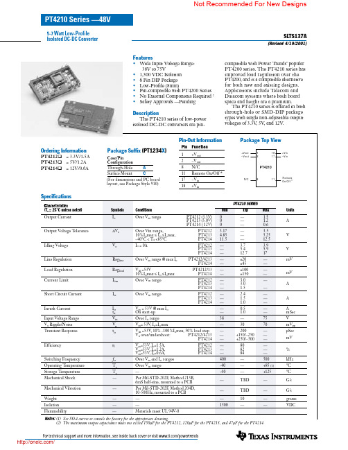
Features•Wide Input Voltage Range: 38V to 75V•1,500 VDC Isolation • 6 Pin DIP Package •Low-Profile (8mm)•Pin-compatible with PT4200 Series •No External Components Required 2•Safety Approvals —PendingDescriptionThe PT4210 series of low-power isolated DC-DC converters are pin-compatible with Power T rends’ popular PT4200 series. The PT4210 series has improved load regulation over the PT4200, and is a compatible alternative for both new and existing designs.Applications include T elecom and Datacom systems where both board space and height are a premium.The PT4210 series is offered in both through-hole or SMD-DIP package types with single non-adjustable output voltages of 3.3V , 5V , and 12V .5-7 Watt Low-Profile Isolated DC-DC ConverterSLTS137A(Revised 4/19/2001)(2)The maximum output capacitance must not exceed 150µF for the PT4212, 120µF for the PT4213, and 47µF for the PT4214.Typical Characteristics5-7 Watt Low-ProfileIsolated DC-DC ConverterPT4210 SeriesUsing the Remote On/Off Function on thePT4210 Isolated 7W DC/DC ConvertersApplications requiring output voltage On/Off control, the PT4210 DC/DC converter series incorporates a “Remote On/Off” control (pin 11). This feature can be used when there is a requirement for the module to be switched off without removing the applied input source voltage.The converter functions normally with Pin 11 open-circuit, providing a regulated output voltage when a valid source voltage is applied to +V in (pin 18), with respect to –V in (pin 17). When a low-level 1 ground signal is applied to pin 11, the converter output will be turned off.Figure 1 shows an application schematic, which details the typical use of the Remote On/Off function. Note the discrete transistor (Q1). The control pin has its own internal pull-up, and must be controlled with an open-collector or open-drain device (See notes 2 & 3). T able 1 gives the input requirements.When placed in the “Off” state, the standby current drawn from the input source is typically reduced to less than 1mA. Table 1; Remote On/Off Control Requirements 1Parameter Min Typ MaxDisable-0.1V— 1.0VEnable 5.0V 3—Open-Circuit 2V o/c [Open-Circuit]——10VI in [pin 11 at –V in]—–100µA—Notes:1.The Remote On/Off control uses –V in (pin 17) as its groundreference. All voltages specified are with respect to –V in.e an open-collector device (preferably a discretetransistor) for the Remote On/Off input. Do not connect apull-up resistor directly to pin 11.3.The Remote On/Off pin may be controlled with devices that havea totem-pole output providing that a blocking diode isused (See Figure 1). The blocking diode is required toprevent current from being injected into On/Off control pin. Note: For TTL devices a pull-up may be required on the cathode side of the blocking diode. This is to guarantee aminimum enable voltage at pin 11 (See Figure 1).4.The PT4210 converters incorporate an “Under-VoltageLockout” (UVLO). The UVLO will keep the module off when the input voltage to the converter is low, regardless of the state of the Remote On/Off control. T able 2 gives the UVLO input voltage thresholds.Table 2; UVLO Thresholds 4Figure 1Turn-On Time: In the circuit of Figure 1, turning Q1 on applies a low-voltage to pin 11 and disables the converter output. Correspondingly, turning Q1 off allows pin 11to be pulled high by an internal pull-up resistor. The converter produces a regulated output voltage within 50ms. Although the rise-time of the output is short (<1ms), the delay time will vary depending upon the input voltage and the module’s internal timing. Figure 2 shows shows an example of the output response for a PT4213 (5.0V), following the turn-off of Q1 at time t =0. The waveform was measured with a 48Vdc input voltage, and 1.2Adc resistive load.Figure 2o-Vo +V-VinSeries V in Range UVLO ThresholdPT421038 – 75V36V ±2Vtime (milli-secs)Suffix A, C(Revised 12/1/2000)PACKAGE INFORMATION AND DIMENSIONSPACKAG PACKAGING INFORMATIONOrderable Device Status (1)Package Type PackageDrawing Pins Package Qty Eco Plan (2)Lead/Ball FinishMSL PeaPT4212A OBSOLETE DIP MODULE EGH6TBD Call TI Call TIPT4212C NRND DIP MODULE EGJ618TBD Call TI Level-1-215CPT4213A NRND DIP MODULE EGH618TBD Call TI Level-1-215CPT4213C NRND DIP MODULE EGJ618TBD Call TI Level-1-215CPT4214A OBSOLETE DIP MODULE EGH6TBD Call TI Call TIPT4214C NRND DIP MODULE EGJ618TBD Call TI Level-1-215C(1) The marketing status values are defined as follows:ACTIVE: Product device recommended for new designs.LIFEBUY: TI has announced that the device will be discontinued, and a lifetime-buy period is in effect.NRND: Not recommended for new designs. Device is in production to support existing customers, but TI does not recommend using this part in a new PREVIEW: Device has been announced but is not in production. Samples may or may not be available.OBSOLETE: TI has discontinued the production of the device.(2) Eco Plan - The planned eco-friendly classification: Pb-Free (RoHS), Pb-Free (RoHS Exempt), or Green (RoHS & no Sb/Br) - please check http://www.tinformation and additional product content details.TBD: The Pb-Free/Green conversion plan has not been defined.Pb-Free (RoHS): TI's terms "Lead-Free" or "Pb-Free" mean semiconductor products that are compatible with the current RoHS requirements for alllead not exceed 0.1% by weight in homogeneous materials. Where designed to be soldered at high temperatures, TI Pb-Free products are suitable fo Pb-Free (RoHS Exempt): This component has a RoHS exemption for either 1) lead-based flip-chip solder bumps used between the die and package, the die and leadframe. The component is otherwise considered Pb-Free (RoHS compatible) as defined above.Green (RoHS & no Sb/Br): TI defines "Green" to mean Pb-Free (RoHS compatible), and free of Bromine (Br) and Antimony (Sb) based flame retard in homogeneous material)(3) MSL, Peak Temp. -- The Moisture Sensitivity Level rating according to the JEDEC industry standard classifications, and peak solder temperature.Important Information and Disclaimer:The information provided on this page represents TI's knowledge and belief as of the date that it is provided. TIprovided by third parties, and makes no representation or warranty as to the accuracy of such information. Efforts are underway to better integrate inf continues to take reasonable steps to provide representative and accurate information but may not have conducted destructive testing or chemical an TI and TI suppliers consider certain information to be proprietary, and thus CAS numbers and other limited information may not be available for releas In no event shall TI's liability arising out of such information exceed the total purchase price of the TI part(s) at issue in this document sold by TI to Cu /IMPORTANT NOTICETexas Instruments Incorporated and its subsidiaries(TI)reserve the right to make corrections,enhancements,improvements and other changes to its semiconductor products and services per JESD46C and to discontinue any product or service per JESD48B.Buyers should obtain the latest relevant information before placing orders and should verify that such information is current and complete.All semiconductor products(also referred to herein as“components”)are sold subject to TI’s terms and conditions of sale supplied at the time of order acknowledgment.TI warrants performance of its components to the specifications applicable at the time of sale,in accordance with the warranty in TI’s terms and conditions of sale of semiconductor products.Testing and other quality control techniques are used to the extent TI deems necessary to support this warranty.Except where mandated by applicable law,testing of all parameters of each component is not necessarily performed.TI assumes no liability for applications assistance or the design of Buyers’products.Buyers are responsible for their products and applications using TI components.To minimize the risks associated with Buyers’products and applications,Buyers should provide adequate design and operating safeguards.TI does not warrant or represent that any license,either express or implied,is granted under any patent right,copyright,mask work right,or other intellectual property right relating to any combination,machine,or process in which TI components or services are rmation published by TI regarding third-party products or services does not constitute a license to use such products or services or a warranty or endorsement e of such information may require a license from a third party under the patents or other intellectual property of the third party,or a license from TI under the patents or other intellectual property of TI.Reproduction of significant portions of TI information in TI data books or data sheets is permissible only if reproduction is without alteration and is accompanied by all associated warranties,conditions,limitations,and notices.TI is not responsible or liable for such altered rmation of third parties may be subject to additional restrictions.Resale of TI components or services with statements different from or beyond the parameters stated by TI for that component or service voids all express and any implied warranties for the associated TI component or service and is an unfair and deceptive business practice. TI is not responsible or liable for any such statements.Buyer acknowledges and agrees that it is solely responsible for compliance with all legal,regulatory and safety-related requirements concerning its products,and any use of TI components in its applications,notwithstanding any applications-related information or support that may be provided by TI.Buyer represents and agrees that it has all the necessary expertise to create and implement safeguards which anticipate dangerous consequences of failures,monitor failures and their consequences,lessen the likelihood of failures that might cause harm and take appropriate remedial actions.Buyer will fully indemnify TI and its representatives against any damages arising out of the use of any TI components in safety-critical applications.In some cases,TI components may be promoted specifically to facilitate safety-related applications.With such components,TI’s goal is to help enable customers to design and create their own end-product solutions that meet applicable functional safety standards and requirements.Nonetheless,such components are subject to these terms.No TI components are authorized for use in FDA Class III(or similar life-critical medical equipment)unless authorized officers of the parties have executed a special agreement specifically governing such use.Only those TI components which TI has specifically designated as military grade or“enhanced plastic”are designed and intended for use in military/aerospace applications or environments.Buyer acknowledges and agrees that any military or aerospace use of TI components which have not been so designated is solely at the Buyer's risk,and that Buyer is solely responsible for compliance with all legal and regulatory requirements in connection with such use.TI has specifically designated certain components which meet ISO/TS16949requirements,mainly for automotive ponents which have not been so designated are neither designed nor intended for automotive use;and TI will not be responsible for any failure of such components to meet such requirements.Products ApplicationsAudio /audio Automotive and Transportation /automotiveAmplifiers Communications and Telecom /communicationsData Converters Computers and Peripherals /computersDLP®Products Consumer Electronics /consumer-appsDSP Energy and Lighting /energyClocks and Timers /clocks Industrial /industrialInterface Medical /medicalLogic Security /securityPower Mgmt Space,Avionics and Defense /space-avionics-defense Microcontrollers Video and Imaging /videoRFID OMAP Mobile Processors /omap TI E2E Community Wireless Connectivity /wirelessconnectivityMailing Address:Texas Instruments,Post Office Box655303,Dallas,Texas75265Copyright©2012,Texas Instruments Incorporated分销商库存信息:TIPT4212A PT4213A PT4213C PT4212C PT4214A PT4214C。
PD43和PD43c介绍
19 to 114mm 17.8 to 991mm 0.076 to 0.25mm 8.38 in 2 to 4 mm
25 to 114mm (1 to 4.5 in) NA 2.5 to 7mil 8.38 in NA 82 mm (3.2 in)
19 to 114 mm (0.75 to 4.5 in) 6.4 mm to 4.8 m (0.25 in to 15.7 ft) 0.061 to 0.26mm 8.38 in 1.2 to 26 mm 80 mm (3.15 in) 1 in 450 m (1475 ft)
打印量(天) 通讯接口 USB Serial Parallel
USB 2.0 RS-232 Optional
USB Device &2 Host Optional Optional
USB 1.1 RS-232 Optional
USB 1.1 RS-232 Optional
USB Device & 2 Host Optional Optional
8 ips 203 dpi &300 dpi 406 dpi 104 mm (4.09 in)
12 ips 203 dpi &300 dpi 406 dpi 104 mm (4.09 in)
最大打印宽度
介质规格 介质宽度 介质长度 介质厚度 标签卷最大直径 标签之间间隔长度 色带卷最大直径 色带芯内径 色带长度
RFID
UHF/HF
UI(用户操作界面)的升级比较
PC23 & PC43&PC43c PM43 & PM43c
PD43 & PD43c
ZM400系列 105SL和Xi4系列
438II客户手册

Motor Analyzer
用户手册
March 2016 (Simplified Chinese)
©2016 Fluke Corporation. All rights reserved. All product names are trademarks of their respective companies.
有限担保和有限责任
Fluke 担保在正常使用和保养的情况下,其产品没有材料和工艺上的缺陷。从寄送之日起,担保期为三年。部件、产品修理 和服务的担保期限为 90 天。本担保仅限于 Fluke 授权零售商的原购买人或最终用户,并且不适用于一次性电池、电缆接 头、电缆绝缘转换接头或 Fluke 认为由于误用、改装、疏忽、污染及意外或异常操作或处理引起的任何产品损坏。 Fluke 担 保软件能依照功能规格正常运行 90 天,并且软件是记录在无缺陷的媒介上。 Fluke 并不担保软件毫无错误或在运行中不会 中断。 Fluke 授权的零售商应仅对最终用户就新的和未使用的产品提供本担保,但无权代表 Fluke 公司提供额外或不同的担保。只 有通过 Fluke 授权的销售店购买的产品或者买方已经按适用的国际价格付款才能享受 Fluke 的担保支持。在一国购买的产品 需在他国修理时, Fluke 有权向买方要求负担重大修理 / 零件更换费用。 Fluke 的担保为有限责任,由 Fluke 决定是否退还购买金额、免费修理或更换在担保期间退还 Fluke 授权服务中心的故障产 品。 如需要保修服务,请与您就近的 Fluke 授权服务中心联系,获得退还授权信息;然后将产品寄至服务中心,并附上产品问题 描述,同时预付运费和保险费 (目的地离岸价格) 。 Fluke 不承担运送途中发生的损坏。在保修之后,产品将被寄回给买方 并提前支付运输费 (目的地交货) 。如果 Fluke 认定产品故障是由于疏忽、误用、污染、修改、意外或不当操作或处理状况 而产生,包括未在产品规定的额定值下使用引起的过压故障;或是由于机件日常使用损耗,则 Fluke 会估算修理费用,在获 得买方同意后再进行修理。在修理之后,产品将被寄回给买方并预付运输费;买方将收到修理和返程运输费用 (寄发地交 货)的帐单。 本担保为买方唯一能获得的全部补偿内容,并且取代所有其它明示或隐含的担保,包括但不限于适销性或满足特殊目的任何 隐含担保。 FLUKE 对任何特殊、间接、偶发或后续的损坏或损失概不负责,包括由于任何原5
IRMCK203;中文规格书,Datasheet资料
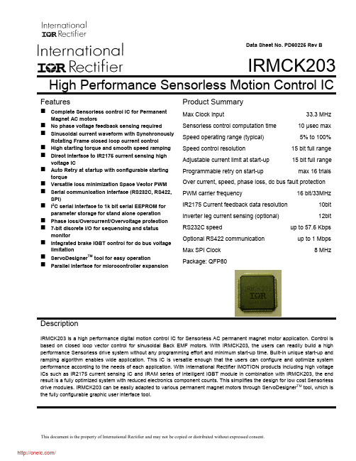
Data Sheet No. PD60225 Rev BIRMCK203High Performance Sensorless Motion Control ICFeaturesComplete Sensorless control IC for PermanentMagnet AC motorsNo phase voltage feedback sensing required Sinusoidal current waveform with SynchronouslyRotating Frame closed loop current control High starting torque and smooth speed ramping Direct interface to IR2175 current sensing highvoltage IC Auto Retry at startup with configurable startingtorque Versatile loss minimization Space Vector PWM Serial communication interface (RS232C, RS422,SPI) I 2C serial interface to 1k bit serial EEPROM forparameter storage for stand alone operation Phase loss/Overcurrent/Overvoltage protection 7-bit discrete I/O for sequencing and statusmonitorIntegrated brake IGBT control for dc bus voltage limitation ServoDesigner TM tool for easy operationParallel interface for microcontroller expansionProduct SummaryMax Clock input33.3 MHz Sensorless control computation time 10 µsec max Speed operating range (typical) 5% to 100% Speed control resolution15 bit full range Adjustable current limit at start-up 15 bit full range Programmable retry on start-upmax 16 trialsOver current, speed, phase loss, dc bus fault protection PWM carrier frequency16 bit/33MHzIR2175 Current feedback data resolution 10bit Inverter leg current sensing (optional) 12bitRS232C speedup to 57.6 Kbps Optional RS422 communication up to 1 MbpsMax SPI Clock 8 MHzPackage: QFP80DescriptionIRMCK203 is a high performance digital motion control IC for Sensorless AC permanent magnet motor application. Control is based on closed loop vector control for sinusoidal Back EMF motors. With IRMCK203, the users can readily build a high performance Sensorless drive system without any programming effort and minimum start-up time. Built-in unique start-up and ramping algorithm enables wide application. This IC is versatile enough that the users can configure and optimize system performance according to the needs of each application. With International Rectifier iMOTION products including high voltage ICs such as IR2175 current sensing IC and IRAM series of Intelligent IGBT module in combination with IRMCK203, the end result is a fully optimized system with reduced electronics component counts. This simplifies the design for low cost Sensorless drive modules. IRMCK203 can be easily adapted to various permanent magnet motors through ServoDesigner TM tool, which is the fully configurable graphic user interface tool.OverviewIRMCK203 is a new International Rectifier integrated circuit device designed for one-chip solution for complete closed loop current and velocity control of a high performance Sensorless drive for PM motors. Unlike a traditional microcontroller or DSP, IRMCK203 does not require any programming to complete complex Sensorless algorithm development. Combined with International Rectifier's high voltage gate drive and current sensing IC, the user can implement complete speed control of PM motors with minimum component count and virtually no design effort. In addition to Sensorless closed loop speed control operation, features such as Start-up retry, Phase Loss detection, Low Loss PWM, Regeneration Braking control and various drive protections are all implemented inside IRMCK203. Analog and digital I/Os can also be configured. Host communication logic contains Asynchronous Communication Interface for RS232C or RS422 communication interface, a fast slave SPI interface and an 8 bit wide Host Parallel Interface. All communication ports have the same access capability to the host register set. The users can write to, and read from the predefined registers to configure and monitor the drive through these communication ports.IRMCK203 Main functions• Complete closed loop current control based on Synchronously Rotating Frame Field Orientation (using Rotor Angle Observer)• Closed loop velocity control based on estimated speed• Configurable parameters (PI controller gains, PI output limit range, current feedbackscaling, PWM carrier frequency) provide adaptation to various PM motors• Built-in Sensorless control logic for start-up, ramping, and running conditions• Auto Retry (programmable) on start-up with configurable torque current limit• Analog reference input (can be used for speed reference)• RS232C/RS422 reference input• Full dynamic braking control for DC bus voltage limitation• Cycle-by-cycle on/off Control for Brake IGBT• Loss minimization Space Vector PWM with deadtime insertion• Build-in two IR2175 current sensing IC interfaces• Phase Loss, Overcurrent (GATEKILL input), Overvoltage, Undervoltage, Overspeed protection• Low cost serial 12bit A/D interface with multiplexer and sample/hold circuit• Optional Inverter Leg (low side) current sensing in lieu of IR2175 IC• 4 channel analog output (PWM)• Local EEPROM for startup initialization of internal data/parameters through host register interface AT24C01A, 128X8• Versatile host communication interfaceRS232C or RS422 host interfaceFast SPI slave host interface with multi-drop capabilityParallel Host interface (total 12 pins)• Multiplexed data/address busAddress EnableRD/WR• Discrete I/Os for Standalone mode operationSTARTSTOP (Input)ESTOP (Input)DIR (Input) FLTCLR (Input) FAULT (Output) SYNC (Output) REDLED (Output)GREENLED (Output)Table of Contents Overview (2)IRMCK203 Main functions (2)IRMCK203 Block Diagrams (7)Basic Block Diagram (7)Input/Output of IRMCK203 (8)Application Connections (12)IC Crystal Clock Circuitry (13)PLL Clock Circuitry (14)Low Pass Filter (14)Implementing the Low Pass Filter Shield (15)Cp Rp and Cs Component Values (15)PLL Reset (15)DC Electrical Characteristics and Operating Conditions (16)Absolute Maximum Ratings (16)Recommended Operating Conditions (16)DC Characteristics (17)Common Quiescent and Leakage Current (17)Input Characteristics – Non Schmitt Inputs (17)Input Characteristics – Schmitt Inputs (17)Output Characteristics (17)Output Characteristics OSC2CLK (18)Pin and I/O Characteristic Table (19)Power Consumption (21)AC Electrical Characteristics and Operating Conditions (22)System Level AC Characteristics (22)Sync Pulse to Sync Pulse Timing (22)FAULT and REDLED Response to GATEKILL (23)Host Interface AC Characteristics (24)SPI Timing (24)Host Parallel Timing (25)Host Parallel Read Cycle (25)Host Parallel Write Cycle (26)Discrete I/O Electrical Characteristics (27)Motion Peripheral Electrical Characteristics (28)PWM Electrical Characteristics (28)IR2175 Interface (28)Analog Interface Electrical Characteristics (29)ADC Timing (29)PLL Interface Electrical Characteristics (30)Appendix A Host Register Map (31)Register Access (31)Host Parallel Access (31)SPI Register Access (31)RS-232 Register Access (31)Write Register Definitions (36)PwmConfig Register Group (Write Registers) (36)CurrentFeedbackConfig Register Group (Write Registers) (37)SystemControl Register Group (Write Registers) (38)TorqueLoopConfig Register Group (Write Registers) (38)VelocityControl Register Group (Write Registers) (39)IRMCK203 FaultControl Register Group (Write Registers) (40)SystemConfig Register Group (Write Registers) (41)EepromControl Registers (Write Registers) (42)ClosedLoopAngleEstimator Registers (Write Registers) (43)OpenLoopAngleEstimator Registers (Write Registers) (44)StartupAngleEstimator Registers (Write Registers) (44)StartupRetrial Registers (Write Registers) (45)PhaseLossDetect Registers (Write Registers) (47)D/AConverter Registers (Write Registers) (47)Factory Test Register (Write Register) (48)Read Register Definitions (49)SystemStatus Register Group (Read Registers) (49)DcBusVoltage Register Group (Read Registers) (49)FocDiagnosticData Register Group (Read Registers) (50)FaultStatus Register Group (Read Registers) (51)VelocityStatus Register Group (Read Registers) (52)CurrentFeedbackOffset Register Group (Read Registers) (53)EepromStatus Registers (Read Registers) (53)FOCDiagnosticDataSupplement Register Group (Read Registers) (54)ProductIdentification Registers (Read Registers) (55)Factory Register (Read Register) (55)Appendix B Package (56)Table of FiguresFigure 1: IRMCS2031 Simplified Blocks (7)Figure 2: Input/Output of IRMCK203 (8)Figure 3: Application Connection of IRMCK203 (12)Figure 4: Oscillator Circuit (13)Figure 5: PLL Low Pass Filter Shielding (14)Figure 6: System Level SYNC To SYNC Timing (22)Figure 7: FAULT and REDLED Response to GATEKILL (23)Figure 8: SPI Timing (24)Figure 9: Host Parallel Read Cycle (25)Figure 10: Host Parallel Write Cycle (26)Figure 11: Discrete I/O Timing (27)Figure 12: PWM Timing (28)Figure 13: IR2175 Interface (28)Figure 14: Top Level ADC Timing (29)Table of TablesTable 1: Typical Values for the Clock Circuit (13)Table 2: PLL Test Pin Assignments (14)Table 3: PLL Low Pass Filter Values (15)Table 4: Absolute Maximum Ratings (16)Table 5: Recommended Operating Conditions (16)Table 6: DC Characteristics (17)Table 7: Non Schmitt Input Characteristics (17)Table 8: Schmitt Input Characteristics (17)Table 9: Output Characteristics (17)Table 10: Output Characteristics OSC2CLK (18)Table 11: Pin and I/O Characteristics (21)Table 12: IRMCK203 Power Consumption (21)Table 13: System Level SYNC to SYNC Timing (22)Table 14: FAULT and REDLED Response to GATEKILL (23)Table 15: SPI Timing (24)Table 16: Host Parallel Read Cycle Timing (25)Table 17: Host Parallel Write Cycle Timing (26)IRMCK203 Block DiagramsBasic Block DiagramFigure 1 shows the basic block diagram of the IRMCK203 surrounded by International Rectifiers’ ICs. Host communications are provided over SPI, RS-232C or Host parallel ports. Two current sensing ICs (IR2175) and a three phase high voltage gate drive typically implement the high voltage / current interface between the IRMCK203 IC and motor.The IRMCK203 can operate in a “stand-alone” mode without the host controller. A serial EEPROM would be utilized to load motor-specific parameters into the IC.AC PowerConfigurable parameters are provided to tailor design to various applications (motor and load). These configurable parameters can be modified via the host register interface through the communication interface. In the IRMCK203 product, a design spread sheet is provided to aid the user for ease of drive start-up, the spread sheet will input high level application data such as motor name plate information, max speed, current limit, speed and current regulator bandwidth, base on this information the program will generate the required configurable parameters. Detail on Drive commissioning is described in the IRMCK203 Application Developer’s Guide.All logic and algorithms are pre-programmed, and the user does not need to make any effort to develop code, alleviating the tedious design process. If needed, the user can configure the drive to tailor the control per specificneeds to meet the required specification. This configuration can be easily done by accessing the host register interface through the communication interface.Input/Output of IRMCK203The I/O signals are shown in Figure 2. The interface signals are divided into sub-groups. For detailed pin assignment, please refer to appendix (Pin definition).PWMUH PWMUL PWMVL BRAKEGATEKILLIFB[0-1]ADCLK ADOUT ADCONVST ADMUX[0-2]RESSAMPLEPWM gate signalInterfaceIR2175 Interface A/D InterfaceSPI Interface Parallel InterfaceLED/StatusPLL Clock ControlCrystalDAC[0-3]D/A Interface (PWM output)RESETNSystem ResetFLTCLROUT Figure 2: Input/Output of IRMCK203Host Interface GroupSignal Input (I) /Output (O)Low (L) /High (H) TrueAsserted FunctionSPICLK IPositive edgesensitiveSPI clockSPIMISO O - Master input and slave output SPIMOSI I - Master output and slave input SPICSN I L SPI chip selectHP_nOE I LParallel data output enable HP_nWE I LParallel data write cycleidentificationHP_D [7:0] I/O - Parallel dataHP_A I HParallel data address cycleidentificationHP_nCS I L Chip select TX O - RS-232 data out RX I - RS-232 data inBAUDSEL[1:0] I H RS-232 baud rate: 00 = 19.3K bps;01 = 38.4K bps10 = 57.6K bps;11 = 1.031250M bpsSYNC O L Start of PWM cycleCLK1XOUT O -33.333 MHz output of PLL. This signal has no phase relationshipwith the OSC1CLK or OSC2CLK inputs.Discrete I/O GroupSignalInput (I) / Output (O)Low (L) / High (H) True AssertedFunctionSTARTSTOP I HStart / Stop command edgesensitiveDIR I HForward/Reverse Directioncommand, level sensitiveFAULTCLR I H Fault ClearESTOP I HEmergency Stop, statesensitivePWEN O H PWM enable/disable state SYNC O H SYNC pulse FAULT O H Fault stateMotion Peripheral GroupSignalInput (I) / Output (O)Low (L) / High (H) True AssertedFunctionPWMUH O PWM phase U high side PWMUL O PWM phase U low side PWMVH O PWM phase V high sidePWHVL O PWM phase V low side PWMWH O PWM phase W high side PWMWL O -PWM phase W low side BRAKE O L IGBT gateGATEKILL I Varies, Based onWrite Register0x0C Bit 7When asserted, negates all sixPWM signals, host writeableIFB0 I - Channel 0 (phase V) IFB1 I - Channel 1 (phase W)Analog Interface GroupSignal Input (I) /Output (O)Low (L) /High (H) TrueAsserted FunctionADCLK ONegative EdgeSensitiveClock to ADS7818ADOUT I - Serial data from ADS7818 DAC [3:0] O - Diagnostic DACADCONVST O LConversion start to ADS7818 RESSAMPLE OSample/hold control signalchannel 0 A/D converterADMUX0 O H Analog input MUX select ADMUX1 O H Analog input MUX selectPLL Interface GroupSignal Input (I) /Output (O)Low (L) /High (H) True AssertedFunctionXPD I L PLL reset RESETN I L Digital logic resetBYPASSCLK I HInternal test pin – force to logiclowBYPASSMODE I HInternal test pin – force to logiclowOSC1CLK I - 33.33 MHz crystal input OSC2CLK I - 33.33 MHz crystal inputPLLTEST I HInternal test pin – force to logiclowCHGO I/O - Low pass filter LPVSS I/O - Low pass filter ground分销商库存信息: IRIRMCK203。
高灵敏度光敏二极管PD438C_S46
上标P照4感明焊峰脚4插上上P照4感明焊峰脚4插 上上上上上耗o电脚 上上上上上上上上上上上上上上上上上上上上上上上上上上上上上上上上上上上上上上上上上上上上上标上标上上上上 上 上上 上 上 上 上 上上 上 上 上 上 上V耗上感技上V上 上 上 上 上P采上式技带上高W上上 上 上 上Tsol上性插带上 上上 上 上 上Topr上-性带~大明技上 上上 上 上 上Tst铅上-4带~大明技上 上 型式小上 上技上 上上上标上 Ta=性技 上上上上上 上 上 上 上 上 上 上上λ带小技上4带带上--上式式带带上n高上上上λp上--上有4带上--上n高上上上VO焊上--上带小感技上--上V上特e=技高W峰c高性,λp=有4带n高上上相sc上--上77上--上μA上特e=技高W峰c高性,λp=有4带n高上上相科上--上77上--上μA上上V耗=技小带V,上上上上上上上上特e=技高W峰c高性上λp=有4带n高上上相采上-上--上感带上nA上V耗=式带小带V上特e=带高W峰c高性上上BV耗上感技上--上--上V上相耗=式带带uA上特e=带高W峰c高性上上焊t上--上44上--上p环上V耗=感小带V上特e=带高W峰c高性上f=式符电z上 峰 上t r峰t f上上--上技带峰技带上上n脚上V耗=式带小带V上耗科=技带Ω上上上上上上上上上上上上标上上上上上上上上上上上上上上上上上上上上上上上上上上上上上上上上上上上上上上上上上上上上上上上上上上标上,上式带带带 峰 小上。
BAT54;BAT54_D87Z;BAT54A;BAT54C;BAT54S;中文规格书,Datasheet资料

intended to be an exhaustive list of all such trademarks.
2Cool¥ AccuPower¥ AX-CAP¥* BitSiC¥ Build it Now¥ CorePLUS¥ CorePOWER¥ CROSSVOLT¥ CTL¥ Current Transfer Logic¥ DEUXPEED® Dual Cool™ EcoSPARK® EfficientMax¥ ESBC¥
®*
The Power Franchise®
TinyBoost¥ TinyBuck¥ TinyCalc¥ TinyLogic® TINYOPTO¥ TinyPower¥ TinyPWM¥ TinyWire¥ TranSiC¥ TriFault Detect¥ TRUECURRENT®* PSerDes¥
2. A critical component in any component of a life support, device, or system whose failure to perform can be reasonably expected to cause the failure of the life support device or system, or to affect its safety or effectiveness.
UHC® Ultra FRFET¥ UniFET¥ VCX¥ VisualMax¥ VoltagePlus¥ XS™
FPS¥ ®
* Trademarks of System General Corporation, used under license by Fairchild Semiconductor.
04 软件需求规格说明-GJB438C模板
编号:版本:状态:密级:分发号:XX软件需求规格说明编制/日期:审核/日期:标审/日期:会签/日期:批准/日期:XX科技有限公司20XX年X月文档修订记录目录1范围 (1)1.1标识 (1)1.2系统概述 (1)1.3文档概述 (1)2引用文档 (1)3需求 (1)3.1要求的状态和方式 (2)3.2软件能力需求 (2)3.2.X(软件能力) (2)3.3软件外部接口需求 (3)3.3.1 接口标识和接口图 (3)3.3.X(接口的项目唯一的标识符) (3)3.4 软件内部接口需求 (6)3.5 软件内部数据需求 (6)3.6 适应性需求 (7)3.7保密性需求 (7)3.8 安全性需求 (7)3.9 软件环境需求 (7)3.11其他质量特性 (8)3.11计算机资源需求 (8)3.11.1计算机硬件需求 (8)3.11.2计算机硬件资源使用需求 (8)3.11.3计算机软件需求 (8)3.11.4计算机通信需求 (9)3.12设计和实现约束 (9)3.13人员需求 (9)3.14训练相关需求 (10)3.15软件保障需求 (10)3.16包装需求 (10)3.17其他需求 (10)3.18需求的优先顺序和关键程度 (10)4合格性规定 (11)5需求可追踪性 (11)8注释 (12)1范围1.1标识【注释:本条应描述本文档所适用的系统和软件的完整标识,适用时,包括其标识号、名称、缩略名、版本号和发布号。
】1.2系统概述【注释:本条应概述本文档所适用的系统和软件的用途。
描述系统与软件的一般特性(如规模、安全性、可靠性、实时性、技术风险等特性);概述系统开发、运行和维护的历史;标识项目的需方、用户、开发方和保障机构等;标识当前和计划的运行现场;列出其他有关文档。
】1.3文档概述【注释:本条应概述本文档的用途和内容,并描述与它的使用有关的保密性方面的要求。
】2引用文档【注释:本章应列出引用文档的编号、标题、编写单位、修订版及日期,还应给出不能通过正常渠道得到的文档的来源。
CPLL66-4160-4380;中文规格书,Datasheet资料
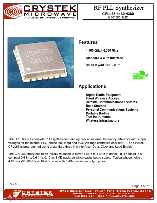
MICROWAVE
A Division of Crystek Corporation
CPLL66-4160-4380
0.60" SQ SMD
Table II shows the details of the four 24 bit registers.
REFERENCE COUNTER LATCH
The CPLL66 is a complete PLL/Synthesizer needing only an external frequency reference and supply voltages for the internal PLL (phase lock loop) and VCO (voltage controlled oscillator). The Crystek CPLL66 is programmed using a standard three line interface (Data, Clock and Load Enable). The CPLL66 family has been initially released to cover 1 GHz to 5 GHz in bands. It is housed in a compact 0.6-in. x 0.6-in. x 0.15-in. SMD package which saves board space. Typical phase noise at 4 GHz is -90 dBc/Hz at 10 kHz offset with 0 dBm minimum output power.
@1kHz offset @10kHz offset @100kHz offset @1MHz offset Power Supply: V1=VCO Supply V2=PLL Supply Supply Current: I1=VCO Input Current I2=PLL Input Current Spurious Suppression PFDSpur Reference Feedthru Harmonic Suppression (2nd Harmonic):
GJB438C模板_软件开发计划(已按标准公文格式校准)
编号:公司简称首字母_系统简称首字母_TF00_V1.0版本:V1.0状态:受控密级:非密分发号:01XX系统软件开发计划编制/日期:__________________审核/日期:__________________标审/日期:__________________会签/日期:__________________批准/日期:__________________XX公司YYYY年MM月文档修订记录目录1范围 (1)1.1标识 (1)1.2系统概述 (1)1.3文档概述 (1)1.4与其他计划之间的关系 (2)2引用文档 (2)3策划背景概述 (3)3.1 系统的需求和约束 (3)3.2 项目文档的需求和约束 (3)3.3 本文档在系统寿命周期中所处的位置 (3)3.4 所选定项目获取策略及有关的要求与约束 (3)3.5 项目进度安排及资源方面的需求与约束 (3)3.6 其他要求和约束 (4)4软件开发活动的总体实施计划 (4)4.1软件开发过程 (4)4.2软件开发总体计划 (5)4.2.1软件开发方法 (5)4.2.2软件产品标准 (5)4.2.3可重用的软件产品 (5)4.2.4关键需求的处理 (6)4.2.5计算机硬件资源的利用 (6)4.2.7需方评审所需访问 (7)5详细的软件开发活动实施计划 (7)5.1项目策划和监控 (7)5.2软件开发环境建立 (8)5.3系统需求分析 (9)5.4系统设计 (9)5.5软件需求分析 (10)5.6软件设计 (10)5.7软件实现和单元测试 (11)5.8单元集成和测试 (11)5.9软件合格性测试 (12)5.10软件/硬件集成和测试 (12)5.11系统合格性测试 (12)5.12软件使用准备 (12)5.13软件移交准备 (12)5.14软件验收支持 (13)5.15软件配置管理 (13)5.16软件产品评价 (13)5.17软件质量保证 (13)5.18纠正措施 (13)5.19联合评审 (14)5.21测量和分析 (14)5.22保密性 (14)5.23分承制方管理 (14)5.24与软件独立验证和确认机构的联系 (14)5.25与相关开发方的协调 (14)5.26项目过程的改进 (15)5.27未提及的其他活动 (15)6进度表和活动网络图 (15)7项目组织和资源 (17)7.1项目组织 (17)7.2项目资源 (21)8注释 (22)1范围1.1标识本文档的标识为:公司简称首字母_系统简称首字母_TF00_V1.0。
LTC4446EMS8E#PBF;LTC4446EMS8E#TRPBF;LTC4446IMS8E#PBF;LTC4446IMS8E#TRPBF;中文规格书,Datasheet资料
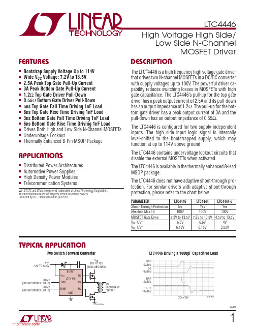
14446fTYPICAL APPLICATIONFEATURESAPPLICATIONSDESCRIPTIONLow Side N-ChannelMOSFET DriverThe L TC ®4446 is a high frequency high voltage gate driver that drives two N-channel MOSFETs in a DC/DC converter with supply voltages up to 100V . The powerful driver ca-pability reduces switching losses in MOSFETs with high gate capacitance. The L TC4446’s pull-up for the top gate driver has a peak output current of 2.5A and its pull-down has an output impedance of 1.2Ω. The pull-up for the bot-tom gate driver has a peak output current of 3A and the pull-down has an output impedance of 0.55Ω.The L TC4446 is confi gured for two supply-independent inputs. The high side input logic signal is internally level-shifted to the bootstrapped supply, which may function at up to 114V above ground.The L TC4446 contains undervoltage lockout circuits that disable the external MOSFETs when activated. The L TC4446 is available in the thermally enhanced 8-lead MSOP package.The L TC4446 does not have adaptive shoot-through pro-tection. For similar drivers with adaptive shoot-through protection, please refer to the chart below.PARAMETER L TC4446L TC4444L TC4444-5Shoot-Through Protection No Yes Yes Absolute Max TS 100V 100V 100V MOSFET Gate Drive 7.2V to 13.5V 7.2V to 13.5V 4.5V to 13.5VV CC UV +6.6V 6.6V 4V V CC UV– 6.15V 6.15V 3.55V nBootstrap Supply Voltage Up to 114V n Wide V CCVoltage: 7.2V to 13.5V n 2.5A Peak Top Gate Pull-Up Current n 3A Peak Bottom Gate Pull-Up Current n 1.2Ω Top Gate Driver Pull-Down n 0.55Ω Bottom Gate Driver Pull-Down n 5ns Top Gate Fall Time Driving 1nF Load n 8ns Top Gate Rise Time Driving 1nF Load n 3ns Bottom Gate Fall Time Driving 1nF Load n 6ns Bottom Gate Rise Time Driving 1nF Loadn Drives Both High and Low Side N-Channel MOSFETs n Undervoltage Lockoutn Thermally Enhanced 8-Pin MSOP PackagenDistributed Power Architecturesn Automotive Power Supplies n High Density Power Modules n Telecommunication SystemsT wo Switch Forward ConverterL TC4446 Driving a 1000pF Capacitive LoadL , L T , L TC and L TM are registered trademarks of Linear Technology Corporation. All other trademarks are the property of their respective owners. Protected by U.S. Patents including 6677210.V BINP 5V/DIVBG 10V/DIV TINP 5V/DIV TG-TS 10V/DIV20ns/DIV4446 TA01b/24446fPIN CONFIGURATIONABSOLUTE MAXIMUM RATINGSSupply VoltageV CC.........................................................–0.3V to 14V BOOST – TS ...........................................–0.3V to 14V TINP Voltage .................................................–2V to 14V BINP Voltage .................................................–2V to 14V BOOST Voltage ........................................–0.3V to 114V TS Voltage ...................................................–5V to 100V Operating Temperature Range (Note 2)....–40°C to 85°C Junction Temperature (Note 3) .............................125°C Storage Temperature Range ...................–65°C to 150°C Lead Temperature (Soldering, 10 sec) ..................300°C(Note 1)1234TINP BINP V CC BG8765TS TG BOOST NCTOP VIEW9MS8E PACKAGE 8-LEAD PLASTIC MSOPT JMAX = 125°C, θJA = 40°C/W , θJC = 10°C/W (NOTE 4)EXPOSED PAD (PIN 9) IS GND, MUST BE SOLDERED TO PCBORDER INFORMATIONELECTRICAL CHARACTERISTICSSYMBOL PARAMETER CONDITIONSMIN TYP MAX UNITS Gate Driver Supply, V CC V CC Operating Voltage7.213.5V I VCCDC Supply Current TINP = BINP = 0V350550μA UVLO Undervoltage Lockout ThresholdV CC Rising V CC Falling Hysteresis l l6.005.606.606.154507.206.70V V mV Bootstrapped Supply (BOOST – TS)I BOOSTDC Supply Current TINP = BINP = 0V 0.12μA Input Signal (TINP , BINP)V IH(BG)BG Turn-On Input Threshold BINP Ramping High l 2.25 2.75 3.25V V IL(BG)BG Turn-Off Input Threshold BINP Ramping Low l 1.85 2.3 2.75V V IH(TG)TG Turn-On Input Threshold TINP Ramping High l 2.25 2.75 3.25V V IL(TG)TG Turn-Off Input Threshold TINP Ramping Lowl 1.852.3 2.75V I TINP(BINP)Input Pin Bias Current ±0.01±2μA High Side Gate Driver Output (TG)V OH(TG)TG High Output Voltage I TG = –10mA, V OH(TG) = V BOOST – V TG 0.7V V OL(TG)TG Low Output Voltage I TG = 100mA, V OL(TG) = V TG –V TSl 120220mV I PU(TG)TG Peak Pull-Up Current l 1.72.5A R DS(TG)TG Pull-Down Resistance l1.22.2ΩThe l denotes the specifi cations which apply over the full operating temperature range, otherwise specifi cations are at T A = 25°C. V CC = V BOOST = 12V , V TS = GND = 0V , unless otherwise noted.LEAD FREE FINISH TAPE AND REEL PART MARKING*PACKAGE DESCRIPTION TEMPERATURE RANGE L TC4446EMS8E#PBF L TC4446EMS8E#TRPBF L TDPZ 8-Lead Plastic MSOP –40°C to 85°C L TC4446IMS8E#PBFL TC4446IMS8E#TRPBFL TDPZ8-Lead Plastic MSOP–40°C to 85°CConsult L TC Marketing for parts specifi ed with wider operating temperature ranges. *The temperature grade is identifi ed by a label on the shipping container .Consult L TC Marketing for information on non-standard lead based fi nish parts.For more information on lead free part marking, go to: http://www.linear .com/leadfree/ For more information on tape and reel specifi cations, go to: http://www.linear .com/tapeandreel//34446fNote 1: Stresses beyond those listed under Absolute Maximum Ratings may cause permanent damage to the device. Exposure to any Absolute Maximum Rating condition for extended periods may affect device reliability and lifetime.Note 2: The L TC4446E is guaranteed to meet specifi cations from 0°C to 85°C. Specifi cations over the –40°C to 85°C operatingtemperature range are assured by design, characterization and correlationELECTRICAL CHARACTERISTICS The l denotes the specifi cations which apply over the full operatingtemperature range, otherwise specifi cations are at T A = 25°C. V CC = V BOOST = 12V , V TS = GND = 0V , unless otherwise noted.SYMBOL PARAMETERCONDITIONSMINTYP MAXUNITS Low Side Gate Driver Output (BG)V OH(BG)BG High Output Voltage I BG = –10mA, V OH(BG) = V CC – V BG0.7VV OL(BG)BG Low Output Voltage I BG = 100mAl 55110mV I PU(BG)BG Peak Pull-Up Current l 23A R DS(BG)BG Pull-Down Resistance l0.55 1.1ΩSwitching Time (BINP (TINP) is Tied to Ground While TINP (BINP) is Switching. Refer to Timing Diagram)t PLH(TG)TG Low-High (Turn-On) Propagation Delay l 2545ns t PHL(TG)TG High-Low (Turn-Off) Propagation Delay l 2240ns t PLH(BG)BG Low-High (Turn-On) Propagation Delay l 1935ns t PHL(BG)BG High-Low (Turn-Off) Propagation Delay l 1430ns t DM(BGTG)Delay Matching BG Turn-Off and TG Turn-On l –151035ns t DM(TGBG)Delay Matching TG Turn-Off and BG Turn-On l –25–325ns t r(TG)TG Output Rise Time 10% – 90%, C L = 1nF 10% – 90%, C L = 10nF880ns ns t f(TG)TG Output Fall Time 10% – 90%, C L = 1nF 10% – 90%, C L = 10nF550ns ns t r(BG)BG Output Rise Time 10% – 90%, C L = 1nF 10% – 90%, C L = 10nF660ns ns t f(BG)BG Output Fall Time 10% – 90%, C L = 1nF 10% – 90%, C L = 10nF 330ns nswith statistical process controls. The L TC4446I is guaranteed over the full –40°C to 85°C operating temperature range.Note 3: T J is calculated from the ambient temperature T A and power dissipation P D according to the following formula: T J = T A + (P D • θJA °C/W)Note 4: Failure to solder the exposed back side of the MS8E package to the PC board will result in a thermal resistance much higher than 40°C/W .TYPICAL PERFORMANCE CHARACTERISTICSV CC Supply Quiescent Current vs VoltageBOOST-TS Supply Quiescent Current vs VoltageV CC Supply Current vs TemperatureV CC SUPPL Y VOL TAGE (V)00Q U I E S C E N T C U R R E N T (μA )501502002506789101112134504446 G011001234514300350400BOOST SUPPL Y VOL TAGE (V)00Q U I E S C E N T C U R R E N T (μA )501502002506789101112134004446 G021001234514300350TEMPERATURE (°C)V C C S U P P L Y C U R R E N T (μA )3503603704446 G03330300–40–25–105203550658095110125380340320310/44446fTYPICAL PERFORMANCE CHARACTERISTICSBoost Supply Current vs TemperatureOutput Low Voltage (V OL ) vs Supply VoltageOutput High Voltage (V OH ) vs Supply VoltageInput Thresholds (TINP , BINP) vs Supply VoltageInput Thresholds (TINP , BINP) vs TemperatureInput Thresholds (TINP , BINP) Hysteresis vs VoltageInput Thresholds (TINP , BINP) Hysteresis vs TemperatureV CC Undervoltage Lockout Thresholds vs TemperatureRise and Fall Time vs V CC Supply VoltageTEMPERATURE (°C)B O O S T S U P P L YC U R R E N T (μA )2503003504446 G041500–40–25–10520355065809511012540020010050SUPPL Y VOL TAGE (V)7O U T P U T V O L T A G E (m V )140104446 G058040891120016012010060121314SUPPL Y VOL TAGE (V)75T G O R B G O U T P U T V O L T A G E (V )689101512911124446 G0671314118101314SUPPL Y VOL TAGE (V)72.1T G O R B G I N P U T T H R E S H O L D (V )2.22.42.52.63.12.8911124446 G072.32.93.02.78101314TEMPERATURE (°C)–25T G O R B G I N P U T T H R E S H O L D (V )2.62.83.0954446 G082.42.22.52.72.92.32.12.053565–10–40110205080125SUPPL Y VOL TAGE (V)78375T G O R B G I N P U T T H R E S H OL D H Y S T E R E S I S (m V )425500911124446 G09400475450101314TEMPERATURE (°C)–40–25375T G O R B G I N P U T T H R E S H O L D H Y S T E R E S I S(m V )425500–105205065804446 G104004754503511095125TEMPERATURE (°C)–406.0V C C S U P L L Y V O L T A G E (V )6.16.36.46.56.7–2535654446 G116.26.62095125110–1055080SUPPL Y VOL TAGE (V)7R I S E /F A L L T I M E (n s )122830222632911124446 G12820161024618148101314/54446fTYPICAL PERFORMANCE CHARACTERISTICSRise and Fall Time vs Load CapacitancePeak Driver (TG, BG) Pull-Up Current vs TemperatureOutput Driver Pull-Down Resistance vs TemperaturePropagation Delay vs V CC Supply VoltagePropagation Delay vs TemperatureLOAD CAPACITANCE (nF)1R I S E /F A L L T I M E (n s )40506094445 G1330200357210468108070TEMPERATURE (°C)–402.0P U L L -U P C U R R E N T (A )2.22.62.83.03.4–2535654446 G142.43.22095125110–1055080TEMPERATURE (°C)–25O U T P U T D R I V E R P U L L -D O W N R E S I S T A C N E (Ω)1.21.62.0954446 G150.80.41.01.41.80.60.253565–10–40110205080125SUPPL Y VOL TAGE (V)710P R O P A G A T I O N D E L A Y (n s )121618203024911124444 G16142628228101314TEMPERATURE (°C)–402P R O P A G A T I O N D E L A Y (n s )717222737–2535654446 G1712322095125110–1055080Switching Supply Current vs Input FrequencySwitching Supply Current vs Load CapacitanceSWITCHING FREQUENCY (kHz)S U P P L Y C U R R E N T (m A )1.52.02.560010004446 G181.00.502004008003.03.54.0LOAD CAPACITANCE (nF)1S U P P L Y C U R R E N T (m A )1010013450.127896104446 G19/64446fPIN FUNCTIONSBLOCK DIAGRAMTINP (Pin 1): High Side Input Signal. Input referenced to GND. This input controls the high side driver output (TG).BINP (Pin 2): Low Side Input Signal. This input controls the low side driver output (BG).V CC (Pin 3): Supply. This pin powers input buffers, logic and the low side gate driver output directly and the high side gate driver output through an external diode con-nected between this pin and BOOST (Pin 6). A low ESR ceramic bypass capacitor should be tied between this pin and GND (Pin 9).BG (Pin 4): Low Side Gate Driver Output (Bottom Gate). This pin swings between V CC and GND.NC (Pin 5): No Connect. No connection required.BOOST (Pin 6): High Side Bootstrapped Supply. An ex-ternal capacitor should be tied between this pin and TS (Pin 8). Normally, a bootstrap diode is connected between V CC (Pin 3) and this pin. Voltage swing at this pin is from V CC – V D to V IN + V CC – V D , where V D is the forward volt-age drop of the bootstrap diode.TG (Pin 7): High Side Gate Driver Output (Top Gate). This pin swings between TS and BOOST .TS (Pin 8): High Side MOSFET Source Connection (Top Source).Exposed Pad (Pin 9): Ground. Must be soldered to PCB ground for optimal thermal performance.TIMING DIAGRAMTINP (BINP)BG (TG)BINP (TINP)TG (BG)/OPERATIONOverviewThe L TC4446 receives ground-referenced, low voltage digi-tal input signals to drive two N-channel power MOSFETs in a synchronous buck power supply confi guration. The gate of the low side MOSFET is driven either to V CC or GND, depending on the state of the input. Similarly, the gate of the high side MOSFET is driven to either BOOST or TS by a supply bootstrapped off of the switching node (TS). Input StageThe L TC4446 employs CMOS compatible input thresholds that allow a low voltage digital signal to drive standard power MOSF ETs. The LTC4446 contains an internal voltage regulator that biases both input buffers for high side and low side inputs, allowing the input thresholds (V IH = 2.75V, V IL = 2.3V) to be independent of variations inV CC. The 450mV hysteresis between V IH and V IL eliminates false triggering due to noise during switching transitions. However, care should be taken to keep both input pins (TINP and BINP) from any noise pickup, especially in high frequency, high voltage applications. The L TC4446 input buffers have high input impedance and draw negligible input current, simplifying the drive circuitry required for the inputs.Output StageA simplifi ed version of the L TC4446’s output stage is shown in Figure 1. The pull-up devices on the BG and TG outputs are NPN bipolar junction transistors (Q1 and Q2). The BG and TG outputs are pulled up to within an NPN V BE (~0.7V) of their positive rails (V CC and BOOST, respectively). Both BG and TG have N-channel MOSFET pull-down devices (M1 and M2) which pull BG and TG down to their nega-tive rails, GND and TS. The large voltage swing of the BG and TG output pins is important in driving external power MOSFETs, whose R DS(ON) is inversely proportional to the gate overdrive voltage (V GS − V TH).Rise/Fall TimeThe L TC4446’s rise and fall times are determined by the peak current capabilities of Q1 and M1. The predriver that drives Q1 and M1 uses a nonoverlapping transition scheme to minimize cross-conduction currents. M1 is fully turned off before Q1 is turned on and vice versa.Since the power MOSFET generally accounts for the ma-jority of the power loss in a converter, it is important to quickly turn it on or off, thereby minimizing the transition time in its linear region. An additional benefi t of a strong pull-down on the driver outputs is the prevention of cross- conduction current. For example, when BG turns the low side (synchronous) power MOSFET off and TG turns the high side power MOSFET on, the voltage on the TS pin will rise to V IN very rapidly. This high frequency positive voltage transient will couple through the C GD capacitance of the low side power MOSFET to the BG pin. If there is an insuffi cient pull-down on the BG pin, the voltage on the BG pin can rise above the threshold voltage of the low side power MOSFET, momentarily turning it back on. With Figure 1. Capacitance Seen by BG and TG During Switching/74446fOPERATIONboth the high side and low side MOSFETs conducting, signifi cant cross-conduction current will fl ow through the MOSFETs from V IN to ground and will cause substantial power loss. A similar effect occurs on TG due to the C GS and C GD capacitances of the high side MOSFET.The powerful output driver of the L TC4446 reduces the switching losses of the power MOSFET, which increase with transition time. The L TC4446’s high side driver is capable of driving a 1nF load with 8ns rise and 5ns fall times using a bootstrapped supply voltage V BOOST-TS of 12V while its low side driver is capable of driving a 1nF Power DissipationTo ensure proper operation and long-term reliability, the L TC4446 must not operate beyond its maximum tem-perature rating. Package junction temperature can be calculated by:T J = T A + P D (θJA)where:T J = Junction temperatureT A = Ambient temperatureP D = Power dissipationθJA = Junction-to-ambient thermal resistance Power dissipation consists of standby and switching power losses:P D = P DC + P AC + P QGwhere:P DC = Quiescent power lossP AC = Internal switching loss at input frequency, f INP QG = Loss due turning on and off the external MOSFET with gate charge QG at frequency f IN load with 6ns rise and 3ns fall times using a supply volt-age V CC of 12V.Undervoltage Lockout (UVLO)The L TC4446 contains an undervoltage lockout detector that monitors V CC supply. When V CC falls below 6.15V, the output pins BG and TG are pulled down to GND and TS, respectively. This turns off both external MOSFETs. When V CC has adequate supply voltage, normal operation will resume.APPLICATIONS INFORMATIONThe L TC4446 consumes very little quiescent current. TheDC power loss at V CC = 12V and V BOOST-TS = 12V is only(350μA)(12V) = 4.2mW.At a particular switching frequency, the internal power lossincreases due to both AC currents required to charge anddischarge internal node capacitances and cross-conduc-tion currents in the internal logic gates. The sum of thequiescent current and internal switching current with noload are shown in the Typical Performance Characteristicsplot of Switching Supply Current vs Input Frequency.The gate charge losses are primarily due to the large ACcurrents required to charge and discharge the capacitanceof the external MOSFETs during switching. For identicalpure capacitive loads C LOAD on TG and BG at switchingfrequency f IN, the load losses would be:P CLOAD = (C LOAD)(f)[(V BOOST-TS)2 + (V CC)2]In a typical synchronous buck confi guration, V BOOST-TSis equal to V CC – V D, where V D is the forward voltagedrop across the diode between V CC and BOOST. If thisdrop is small relative to V CC, the load losses can beapproximated as:P CLOAD = 2(C LOAD)(f IN)(V CC)2/84446fAPPLICATIONS INFORMATIONUnlike a pure capacitive load, a power MOSF ET’s gate capacitance seen by the driver output varies with its V GS voltage level during switching. A MOSFET’s capacitive load power dissipation can be calculated using its gate charge, Q G. The Q G value corresponding to the MOSFET’s V GS value (V CC in this case) can be readily obtained from the manufacturer’s Q G vs V GS curves. For identical MOSFETs on TG and BG:P QG = 2(V CC)(Q G)(f IN)To avoid damage due to power dissipation, the L TC4446 includes a temperature monitor that will pull BG and TG low if the junction temperature rises above 160°C. Normal operation will resume when the junction temperature cools to less than 135°C.Bypassing and GroundingThe LTC4446 requires proper bypassing on the V CC and V BOOST-TS supplies due to its high speed switching (nanoseconds) and large AC currents (Amperes). Careless component placement and PCB trace routing may cause excessive ringing.To obtain the optimum performance from the L TC4446: A. Mount the bypass capacitors as close as possible between the V CC and GND pins and the BOOST and TS pins. The leads should be shortened as much as possible to reduce lead inductance.B. Use a low inductance, low impedance ground plane to reduce any ground drop and stray capacitance. Remember that the L TC4446 switches greater than 3A peak currents and any signifi cant ground drop will degrade signal integrity.C. Plan the power/ground routing carefully. Know where the large load switching current is coming from and going to. Maintain separate ground return paths for the input pin and the output power stage.D. Keep the copper trace between the driver output pin and the load short and wide.E. Be sure to solder the Exposed Pad on the back side of the L TC4446 package to the board. Correctly soldered to a 2500mm2 doublesided 1oz copper board, the L TC4446 has a thermal resistance of approximately 40°C/W for the MS8E package. Failure to make good thermal contact between the exposed back side and the copper board will result in thermal resistances far greater than 40°C/W./94446f104446fTYPICAL APPLICATIONL T C 3722/L T C 4446 420W 36V -72V I N t o 12V /35A I s o l a t e d F u l l -B r i d g e S u p p l yL 1V I –V I 36V T /分销商库存信息:LINEAR-TECHNOLOGYLTC4446EMS8E#PBF LTC4446EMS8E#TRPBF LTC4446IMS8E#PBF LTC4446IMS8E#TRPBF。
光敏二极管规格书PD438

5
30
nA
VR=10.0V Ee=0mW/cm2
反向击穿电压
BVR
35
--
--
V
IR=100uA Ee=0mW/cm2
总计电容
Ct
--
44
--
pF
VR=3.0V Ee=0mW/cm2f=1MHz
上升/下降时间
tr/tf
--
50/50
ห้องสมุดไป่ตู้nS
VR=10.0V RL=50Ω
典型光电特性图:
产品包装:
防静电包装袋, 1000只/袋.
极限参数值:
参 数
符 号
最 大 值
单 位
反 向 电 压
VR
35
V
耗 散 功 率
Pd
150
mW
焊 接 温 度
Tsol
260
℃
工 作 温 度
Topr
-20~+85
℃
存 储 温 度
Tstg
-40~+85
℃
注:*1. 焊接时间≤ 5 秒
光电特性: (Ta=25℃)
项 目
符号
最小值
典型值
最大值
单位
条件
光谱带宽
光敏二极管
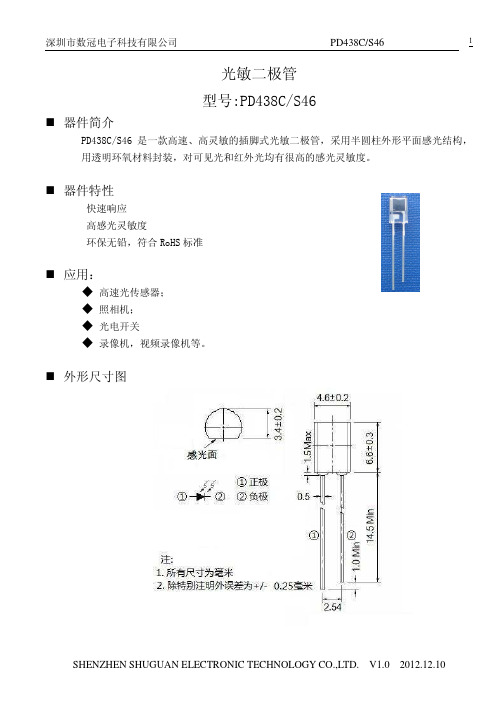
型号:PD438
器件简介
PD438是一款高速、高灵敏的插脚式光敏二极管,采用半圆柱外形平面感光结构,用透明环氧材料封装,对可见光和红外光均有很高的感光灵敏度。
器件特性
快速响应
高感光灵敏度
环保无铅,符合RoHS标准
应用:
高速光传感器;
照相机;
光电开关
录像机,视频录像机等。
外形尺寸图
AP439P资料
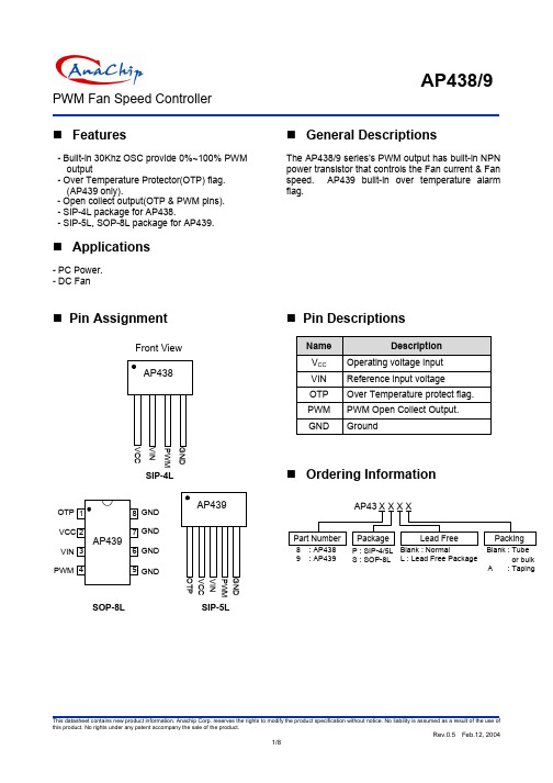
PWM Fan Speed ControllerFeatures- Built-in 30Khz OSC provide 0%~100% PWM output- Over Temperature Protector(OTP) flag. (AP439 only).- Open collect output(OTP & PWM pins). - SIP-4L package for AP438.- SIP-5L, SOP-8L package for AP439.Applications- PC Power. - DC FanGeneral DescriptionsThe AP438/9 series’s PWM output has built-in NPN power transistor that controls the Fan current & Fan speed. AP439 built-in over temperature alarm flag.Pin AssignmentVCCVIN Front View GNDPWMVINSOP-8L SIP-5LSIP-4LGNDOTP GND VIN GNDGNDPWMPin DescriptionsName DescriptionV CC Operating voltage input VIN Reference input voltage OTP Over Temperature protect flag. PWM PWM Open Collect Output.GND GroundOrdering InformationS : SOP-8L 9 : AP439L : Lead Free Packageor bulkA : TapingPWM Fan Speed ControllerBlock DiagramsOTPPWMVINGNDAbsolute Maximum RatingsSymbol Parameter Rating UnitVoltage 20 V V CC SupplyVIN Inputvoltage 20 V OTP Over temperature output. 20 VPWM Output voltage to Ground 20 VP D Power dissipation (SIP-4/5L) 0.5 WP D Power dissipation (SOP-8L) 0.8 WT ST Storage temperature range -65 to 150 o CT OP Operating temperature range 0 to +85 o CV OP Operating voltage range 7.0 to 18 VPWM Fan Speed ControllerElectrical CharacteristicsUnless otherwise specified, guaranteed for Tj=25OC , V CC =12V .Symbol Parameter Conditions Min. Typ. Max. UnitsV CC Supply Voltage 7.0 - 18V I IN Input Bias Current(V IN Pin) V IN =2.0V, 0.5 2 7 uA V IN Input Voltage Range 0 VCC-0.5 V DUTY PWM duty cycle range 0 100 % V IN(OTP) OTP Detect Voltage3.3 3.4 3.5 V V IN(Release) OTP release Voltage 2.65 2.75 2.85 V V IN(HS) OTP detect Voltage Hysteresis 450 650 850 mV V IN(PWM0) Max Input voltage of 0% PWM 0.75 0.8 0.85 V V IN(PWM100) Min Input voltage of 100% PWM 2.80 2.85 2.90 VI S Supply Current Output floating 2.5 mAV PWM(ON) PWM transistor ON voltageI PWM =500mAcontinued1.1 1.3 V I PWM Max. sink current 500 mA V OTP(L) OTP low level voltage I OTP =20mA 0.3 0.6 V I OTPMax. sink current20 mA F OSC OSC Frequency0O C<T J <85O C 22 30 38 KhzApplication CircuitPWM Fan Speed ControllerTypical CharacteristicsPWM Fan Speed ControllerMarking Information(1) SIP4/5L(2) SOP-8LSOP-8L( Top View )Logo~Part NumberPWM Fan Speed ControllerPackage Information(1) Package Type: SIP-4L ( unit: mm / [inch] )0.004]0.13.65±±0.001]0.03±±0.03±0.001]±0.001][0.150±1.27[0.0500.11.42±[0.056±0.001][0.015± 1.25±0.049]±1.03±[0.041±0.11.55±°°7~°30.1±0.004]±PWM Fan Speed ControllerPackage Information (Continued)(2) Package Type: SIP-5L ( unit: mm / [inch] )0.001][0.0150.030.38±±0.001][0.0370.030.95±±[0.1440.13.65±±0.003][0.0190.10.48±±0.001][0.015±°°3~[0.5630.314.3±±[0.0610.11.55±±0.003]0.1±±°5~2°°3~2PWM Fan Speed ControllerPackage Information (Continued)(3) Package Type: SOP-8LDimensions In Millimeters Dimensions In InchesSymbolMin. Nom. Max. Min. Nom. Max.A 1.40 1.60 1.75 0.055 0.063 0.069A1 0.10 - 0.25 0.040 - 0.100A2 1.30 1.45 1.50 0.051 0.057 0.059B 0.33 0.41 0.51 0.013 0.016 0.0200.008 0.010C 0.19 0.20 0.25 0.0075D 4.80 5.05 5.30 0.189 0.199 0.209E 3.70 3.90 4.10 0.146 0.154 0.161e - 1.27 - - 0.050 -H 5.79 5.99 6.20 0.228 0.236 0.244L 0.38 0.71 1.27 0.015 0.028 0.050y - - 0.10 - - 0.004θ0O - 8O0O - 8O。
- 1、下载文档前请自行甄别文档内容的完整性,平台不提供额外的编辑、内容补充、找答案等附加服务。
- 2、"仅部分预览"的文档,不可在线预览部分如存在完整性等问题,可反馈申请退款(可完整预览的文档不适用该条件!)。
- 3、如文档侵犯您的权益,请联系客服反馈,我们会尽快为您处理(人工客服工作时间:9:00-18:30)。
Technical Data Sheet 4.8mm Semi-Lens Silicon PIN PhotodiodePD438CFeatures․Fast response times ․High photo sensitivity ․Small junction capacitance ․Pb free ․The product itself will remain within RoHS compliant version.DescriptionsPD438C is a high speed and sensitive PIN photodiode in a cylindrical side view plastic package. Due to its water clear epoxy the device is sensitive to visible and infrared radiation.Applications․High speed photo detector ․Camera ․Optoelectronic switch ․VCRs , Video cameraDevice Selection GuideLED Part No. PD Chip Material Silicon Lens Color Water clearEverlight Electronics Co., Ltd. Device No:DPD-043-021http:\\ Prepared date:07-20-2005Rev 2Page: 1 of 7Prepared by:Jaine Tsai/PD438CPackage DimensionsNotes: 1.All dimensions are in millimeters 2.Tolerances unless dimensions ±0.25mmAbsolute Maximum Ratings (Ta=25℃)Parameter Reverse Voltage Power Dissipation Lead Soldering Temperature Operating Temperature Symbol VR Pd Tsol Topr Rating 32 150 260 -25 ~ +85 -40 ~ +85 Units V mW ℃ ℃ ℃Storage Temperature Tstg Notes: *1:Soldering time≦5 seconds.Everlight Electronics Co., Ltd. Device No:DPD-043-021http:\\ Prepared date:07-20-2005Rev 2Page: 2 of 7Prepared by:Jaine Tsai/PD438CElectro-Optical Characteristics (Ta=25℃)Parameter Rang of Spectral Bandwidth Wavelength of Peak Sensitivity Open-Circuit Voltage Short- Circuit Current Reverse Light Current Dark Current Reverse Breakdown Total Capacitance Rise/Fall Time Symbol λ0.5 λp VOC ISC IL Id BVR Ct tr/tf Condition --------Ee=5m W/cm2 λp=940nm Ee=1m W/cm2 λp=940nm Ee=1m W/cm2 λp=940nm VR=5V Ee=0m W/cm2 VR=10V Ee=0m W/cm2 IR=100μA Ee=0m W/cm2 VR=3V f=1MHZ VR=10V RL=1KΩ Min. 400 ------10.2 --32 ----Typ. --940 0.35 18 18 5 170 25 50/50 Max. 1100 ------μA --30 ------nA V Units nm nm VpF nSEverlight Electronics Co., Ltd. Device No:DPD-043-021http:\\ Prepared date:07-20-2005Rev 2Page: 3 of 7Prepared by:Jaine Tsai/PD438CTypical Electro-Optical Characteristics CurvesFig.1 Power Dissipation vs. Ambient Temperature200 150 100Fig.2 Spectral Sensitivity1.0 Ta=25 C 0.8 0.6 0.4500.20 -25 0 25 50 75 85 1000100 300 500 700 900 1100 1300Fig.3 Dark Current vs. Ambient Temperature1000Fig. 4 Reverse Light Current vs. Ee40 30100201010 VR=5V 0.5 1 1.52VR=10V 1 20 40 60 80 1000 3Everlight Electronics Co., Ltd. Device No:DPD-043-021http:\\ Prepared date:07-20-2005Rev 2Page: 4 of 7Prepared by:Jaine Tsai/PD438CTypical Electro-Optical Characteristics CurvesFig.5 Terminal Capacitance vs. Reverse Voltage Fig.6 Response Time vs. Load Resistance102180 60 40f=1MHZ VR=3VVR=10V O Ta=25 C10 10 10 100t-120-2-300.1110100101102103104105Everlight Electronics Co., Ltd. Device No:DPD-043-021http:\\ Prepared date:07-20-2005Rev 2Page: 5 of 7Prepared by:Jaine Tsai/PD438CReliability Test Item And Condition The reliability of products shall be satisfied with items listed below. Confidence level:90% LTPD:10% NO. Item Test Conditions Test Hours/ Cycles 10secs 300Cycles Sample Sizes 22pcs 22pcs IL≦L×0.8 L:Lower 300Cycles 22pcs Specification Limit 0/1 Failure Judgement Criteria Ac/R e 0/1 0/11 2Solder heatTEMP.:260℃±5℃ 15mins 5mins 15mins 5mins 10secs 5minsTemperature Cycle H : +100℃ L : -40℃3Thermal ShockH :+100℃ L :-10℃4 5 6 7High Temperature TEMP.:+100℃ Storage Low Temperature TEMP.:-40℃ Storage DC Operating Life High Temperature/ High Humidity VR=5V 85℃ / 85% R.H1000hrs 1000hrs 1000hrs 1000hrs22pcs 22pcs 22pcs 22pcs0/1 0/1 0/1 0/1Everlight Electronics Co., Ltd. Device No:DPD-043-021http:\\ Prepared date:07-20-2005Rev 2Page: 6 of 7Prepared by:Jaine Tsai/PD438CPacking Quantity Specification1.500PCS/1Bag,6Bags/1Box 2.10Boxes/1CartonLabel Form SpecificationCPN: Customer’s Production Number P/N : Production Number QTY: Packing Quantity CAT: Ranks HUE: Peak Wavelength REF: Reference LOT No: Lot Number MADE IN TAIWAN: Production PlaceRoHSPD438CNotes1. Above specification may be changed without notice. EVERLIGHT will reserve authority on material change for above specification. 2. When using this product, please observe the absolute maximum ratings and the instructions for using outlined in these specification sheets. EVERLIGHT assumes no responsibility for any damage resulting from use of the product which does not comply with the absolute maximum ratings and the instructions included in these specification sheets. 3. These specification sheets include materials protected under copyright of EVERLIGHT corporation. Please don’t reproduce or cause anyone to reproduce them without EVERLIGHT’s consent.EVERLIGHT ELECTRONICS CO., LTD. Office: No 25, Lane 76, Sec 3, Chung Yang Rd, Tucheng, Taipei 236, Taiwan, R.O.C Tel: 886-2-2267-2000, 2267-9936 Fax: 886-2267-6244, 2267-6189, 2267-6306 http:\\Everlight Electronics Co., Ltd. Device No:DPD-043-021http:\\ Prepared date:07-20-2005Rev 2Page: 7 of 7Prepared by:Jaine Tsai/分销商库存信息:EVERLIGHT PD438C。