NTD3055-094中文资料
SDM3055X-E 数字万用表 数据手册说明书
0.060+ 0.004
0.0015+ 0.0005
200 μA
< 8 mV
0.200+ 0.004
0.003+ 0.001
2 mA
< 80 mV
0.200+ 0.004
0.002+ 0.001
直流电流
20 mA 200 mA
< 0.05 V < 0.5 V
0.200+ 0.004 0.200+ 0.004
2、4 线电阻测量:200Ω,2K,20K,200K, 2M,10M,100MΩ
电容测量:2 nF,20nF,200nF,2μF,200μF, 10000μF
连通性测试:量程固定在 2KΩ
二极管测试:0~4V 阀值可调
频率测量:20 Hz ~ 1MHz
周期测量:1 μs ~ 0.05 s
温度测量:支持热电偶,热电阻温度传感器 数学运算功能
0.0100+ 0.0005
100 MΩ
200 nA || 10 MΩ 1.750+ 0.004
0.2000+ 0.0005
二极管测试
0~2V [6] 2~4V
1 mA 1 mA
0.060+ 0.020 0.350+ 0.020
0.0050+ 0.0005 0.0050+ 0.0005
连续性测试
2000 Ω
准确度指标 ±(%读数+%量程)【1】
一年精度 23℃ ± 5℃
2.0 + 0.10 1.0 + 0.05 0.6 + 0.05 1.0 + 0.05 3.0 + 0.05 2.0 + 0.10 1.0 + 0.05 0.6 + 0.05 1.0 + 0.05 3.0 + 0.05 2.0 + 0.10 1.0 + 0.05 0.6 + 0.05 1.0 + 0.05 3.0 + 0.05 2.0+ 0.10 1.0 + 0.05 0.6 + 0.05 1.0 + 0.05 3.0 + 0.05 2.0 + 0.10 1.0 + 0.05 0.6 + 0.05 1.0 + 0.05 3.0 + 0.05 2.0 + 0.10 0.50 + 0.10 2.50 + 0.20 2.0 + 0.10 0.50 + 0.10 2.50 + 0.20 2.0 + 0.20 0.50 + 0.20 2.50 + 0.20 1.5 + 0.15 0.50 + 0.15 2.50 + 0.20
lm2904中文资料
lm2904中文资料LM2439 视频信号输出集成电路LM2453 视频信号输出集成电路LM2577 稳压集成电路LM2595 直流变换集成电路LM270H 自动增益及静噪控制集成电路LM2808N 伴音中频放大、鉴频及功率放大集成电路LM2904 双运算放大集成电路LM3065N 伴音中频放大、鉴频及前置放大集成电路LM3089 调频中频放大集成电路LM311N 电压比较运放集成电路LM317T 三端电源稳压1.5A集成电路LM324 四运算放大集成电路LM324M 四运算放大集成电路LM3361 解调集成电路LM33T 三端电源稳压-26V集成电路LM358 双运算放大集成电路LM358PS-T1 双运算放大集成电路LM3656 伴音中频放大、鉴频及前置放大集成电路LM377 双声道音频功率放大集成电路LM378 双声道音频功率放大集成电路LM380 场扫描输出集成电路LM381 运算放大集成电路LM382 宽带放大集成电路LM384 音频功率放大集成电路LM386 音频功率放大集成电路LM387 宽带放大集成电路LM3875T 音频功率放大集成电路LM3886 音频功率放大集成电路LM3915 发光二极管十位显示驱动集成电路LM399 基准稳压集成电路LM4500A 调频立体声解码集成电路LM4610 音调、音量、平衡调节集成电路LM4765 双声道音频功率放大30W×2集成电路LM741CN 运算放大集成电路LM79052 三端电源稳压-5.2V/1A集成电路LM8915N 显示驱动集成电路LN5241RA89 显示驱动集成电路LP62S512AX-70LLT 存储集成电路LPUVCP-96 端口功能扩展集成电路LR37632 伺服集成电路LR381641 主轴、字符控制集成电路LS0072 变音集成电路LSC4350 屏幕显示控制集成电路LSC4584P2 屏幕显示控制集成电路LT1074 开关电源稳压集成电路LT1109 升压稳压集成电路LTC1147 直流变换集成电路LTC1148 直流变换集成电路LTV1817 光电耦合集成电路LUKS-5140-M2 微处理集成电路LV1011 人工智能处理集成电路LV1100 音频信号处理集成电路LVA501 视频信号处理集成电路LVA521 制式切换集成电路M11B416256A 存储集成电路M1418VVW 微处理集成电路M2063SP 制式转换集成电路M208 系统控制集成电路M24C08 存储集成电路M24C128-WMN6 存储集成电路M27V201-200N6 中文字库集成电路M28F101AVPAD 存储集成电路M3004LAB1 红外遥控信号发射集成电路M32L1632512A 存储集成电路M34300-012SP 微处理集成电路M34300-628SP 微处理集成电路M34300M4-012SP 微处理集成电路M34300N4-011SP 微处理集成电路M34300N4-012SP 微处理集成电路M34300N4-555SP 微处理集成电路M34300N4-567SP 微处理集成电路M34300N4-584SP 微处理集成电路M34300N4-587SP 微处理集成电路M34300N4-628SP 微处理集成电路M34300N4-629SP 微处理集成电路M34300N4-657SP 微处理集成电路M34302M8-612SP 微处理集成电路M37100M8-616SP 微处理集成电路M37102M8-503SP 微处理集成电路M37103M4-750SP 微处理集成电路M37201M6 微处理集成电路M37204M8-852SP 微处理集成电路M37210M2-609SP 微处理集成电路M37210M3-010SP 微处理集成电路M37210M3-550SP 微处理集成电路M37210M3-603SP 微处理集成电路M37210M3-800SP 微处理集成电路M37210M3-901SP 微处理集成电路M37210M3-902SP 微处理集成电路M37210M4-650SP 微处理集成电路M37210M4-688微处理集成电路M37210M4-705SP 微处理集成电路M37210M4-786SP 微处理集成电路M37211M2-604SP 微处理集成电路M37211M2-609SP 微处理集成电路。
NTD3055L104型号N-通道电源MOSFET数据手册说明书

NTD3055L104T4G NTD3055L104-1G NTD3055L104T4G.NTD3055L104,NTDV3055L104Power MOSFET12 A, 60 V, Logic Level N−ChannelDPAK/IPAKDesigned for low voltage, high speed switching applications in power supplies, converters and power motor controls and bridge circuits. Features•Lower R DS(on)•Lower V DS(on)•Tighter V SD Specification•Lower Diode Reverse Recovery Time•Lower Reverse Recovery Stored Charge•NTDV and STDV Prefixes for Automotive and Other Applications Requiring Unique Site and Control Change Requirements;AEC−Q101 Qualified and PPAP Capable•These Devices are Pb−Free and are RoHS CompliantTypical Applications•Power Supplies•Converters•Power Motor Controls•Bridge CircuitsMAXIMUM RATINGS (T J = 25°C unless otherwise noted)Rating Symbol Value Unit Drain−to−Source Voltage V DSS60Vdc Drain−to−Gate Voltage (R GS = 10 M W)V DGR60VdcGate−to−Source Voltage, Continuous − Non−Repetitive (t p v10 ms)V GSV GS"15"20VdcDrain Current− Continuous @ T A = 25°C − Continuous @ T A = 100°C − Single Pulse (t p v10 m s)I DI DI DM121045AdcApkTotal Power Dissipation @ T A = 25°CDerate above 25°CTotal Power Dissipation @ T A = 25°C (Note 1) Total Power Dissipation @ T A = 25°C (Note 2)PD480.322.11.5WW/°CWWOperating and Storage Temperature Range T J, T stg−55 to+175°CSingle Pulse Drain−to−Source Avalanche Energy − Starting T J = 25°C(V DD = 25 Vdc, V GS = 5.0 Vdc, L = 1.0 mH I L(pk) = 11 A, V DS = 60 Vdc)E AS61mJThermal Resistance, − Junction−to−Case − Junction−to−Ambient (Note 1)− Junction−to−Ambient (Note 2)R q JCR q JAR q JA3.1371.4100°C/WMaximum Lead Temperature for Soldering Purposes, 1/8″from case for 10 secondsT L260°CStresses exceeding those listed in the Maximum Ratings table may damage the device. If any of these limits are exceeded, device functionality should not be assumed, damage may occur and reliability may be affected.1.When surface mounted to an FR4 board using 1″ pad size,(Cu Area 1.127 in2).2.When surface mounted to an FR4 board using the minimum recommendedpad size, (Cu Area 0.412 in2).N−Channel60 V104 m WR DS(on) TYP12 AI D MAXV(BR)DSSSee detailed ordering and shipping information in the package dimensions section on page 7 of this data sheet.ORDERING INFORMATION1Gate3Source2Drain4DrainDPAKCASE 369CSTYLE 2MARKING DIAGRAMS& PIN ASSIGNMENTSGate SourceDrain4IPAKCASE 369DSTYLE 2AYWW55L14GA= Assembly Location*55L104= Device CodeY= YearWW= Work WeekG= Pb−Free Package* The Assembly Location code (A) is front side optional. In cases where the Assembly Location is stamped in the package, the front side assembly code may be blank.ELECTRICAL CHARACTERISTICS(T J = 25°C unless otherwise noted)Characteristic Symbol Min Typ Max Unit OFF CHARACTERISTICSDrain−to−Source Breakdown Voltage (Note 3) (V GS = 0 Vdc, I D = 250 m Adc) Temperature Coefficient (Positive)V(BR)DSS60−7062.9−−VdcmV/°CZero Gate Voltage Drain Current(V DS = 60 Vdc, V GS = 0 Vdc)(V DS = 60 Vdc, V GS = 0 Vdc, T J = 150°C)I DSS−−−−1.010m AdcGate−Body Leakage Current (V GS = ±15Vdc, V DS = 0 Vdc)I GSS−−±100nAdc ON CHARACTERISTICS (Note 3)Gate Threshold Voltage (Note 3)(V DS = V GS, I D = 250 m Adc)Threshold Temperature Coefficient (Negative)V GS(th)1.0−1.64.22.0−VdcmV/°CStatic Drain−to−Source On−Resistance (Note 3) (V GS = 5.0 Vdc, I D = 6.0 Adc)R DS(on)−89104m WStatic Drain−to−Source On−Voltage (Note 3) (V GS = 5.0 Vdc, I D = 12 Adc)(V GS = 5.0 Vdc, I D = 6.0 Adc, T J = 150°C)V DS(on)−−0.980.861.50−VdcForward Transconductance (Note 3) (V DS = 8.0 Vdc, I D = 6.0 Adc)g FS−9.1−mhos DYNAMIC CHARACTERISTICSInput Capacitance(V DS = 25 Vdc, V GS = 0 Vdc,f = 1.0 MHz)C iss−316440pFOutput Capacitance C oss−105150 Transfer Capacitance C rss−3570 SWITCHING CHARACTERISTICS (Note 4)Turn−On Delay Time(V DD= 30 Vdc, I D = 12 Adc,V GS = 5.0 Vdc, R G = 9.1 W) (Note 3)t d(on)−9.220nsRise Time t r−104210 Turn−Off Delay Time t d(off)−1940 Fall Time t f−40.580Gate Charge(V DS = 48 Vdc, I D = 12 Adc,V GS = 5.0 Vdc) (Note 3)Q T−7.420nC Q1− 2.0−Q2− 4.0−SOURCE−DRAIN DIODE CHARACTERISTICSForward On−Voltage(I S = 12 Adc, V GS = 0 Vdc) (Note 3)(I S = 12 Adc, V GS = 0 Vdc, T J = 150°C)V SD−−0.950.821.2−VdcReverse Recovery Time(I S = 12 Adc, V GS = 0 Vdc,dI S/dt = 100 A/m s) (Note 3)t rr−35−ns t a−21−t b−14−Reverse Recovery Stored Charge Q RR−0.04−m C Product parametric performance is indicated in the Electrical Characteristics for the listed test conditions, unless otherwise noted. Product performance may not be indicated by the Electrical Characteristics if operated under different conditions.3.Pulse Test: Pulse Width ≤300 m s, Duty Cycle ≤ 2%.4.Switching characteristics are independent of operating junction temperatures.TYPICAL CHARACTERISTICS0.120.080.0400.32110010,000V DS , DRAIN−TO−SOURCE VOLTAGE (VOLTS)I D , D R A I N C U R R E N T (A M P S )V GS , GATE−TO−SOURCE VOLTAGE (VOLTS)Figure 1. On−Region CharacteristicsFigure 2. Transfer CharacteristicsI D , D R A I N C U R R E N T (A M P S )Figure 3. On−Resistance versusGate−to−Source VoltageI D , DRAIN CURRENT (AMPS)Figure 4. On−Resistance versus Drain Currentand Gate VoltageI D , DRAIN CURRENT (AMPS)R D S (o n ), D R A I N −T O −S O U R C E R E S I S T A N C E (W )R D S (o n ), D R A I N −T O −S O U R C E R E S I S T A N C E (W )Figure 5. On−Resistance Variation withTemperature T J , JUNCTION TEMPERATURE (°C)Figure 6. Drain−to−Source Leakage Currentversus VoltageV DS , DRAIN−TO−SOURCE VOLTAGE (VOLTS)R D S (o n ), D R A I N −T O −S O U R C E R E S I S T A N C E (N O R M A L I Z E D )I D S S , L E A K A G E (n A )−505025−257512510012.5640302060101501753.5450101.5234.555.50.240.280.200.161000POWER MOSFET SWITCHINGSwitching behavior is most easily modeled and predicted by recognizing that the power MOSFET is charge controlled. The lengths of various switching intervals (D t)are determined by how fast the FET input capacitance can be charged by current from the generator.The published capacitance data is difficult to use for calculating rise and fall because drain−gate capacitance varies greatly with applied voltage. Accordingly, gate charge data is used. In most cases, a satisfactory estimate of average input current (I G(A V)) can be made from a rudimentary analysis of the drive circuit so that t = Q/I G(A V)During the rise and fall time interval when switching a resistive load, V GS remains virtually constant at a level known as the plateau voltage, V SGP . Therefore, rise and fall times may be approximated by the following:t r = Q 2 x R G /(V GG − V GSP )t f = Q 2 x R G /V GSPwhereV GG = the gate drive voltage, which varies from zero to V GG R G = the gate drive resistanceand Q 2 and V GSP are read from the gate charge curve.During the turn−on and turn−off delay times, gate current is not constant. The simplest calculation uses appropriate values from the capacitance curves in a standard equation for voltage change in an RC network. The equations are:t d(on) = R G C iss In [V GG /(V GG − V GSP )]t d(off) = R G C iss In (V GG /V GSP )The capacitance (C iss ) is read from the capacitance curve at a voltage corresponding to the off−state condition when calculating t d(on) and is read at a voltage corresponding to the on−state when calculating t d(off).At high switching speeds, parasitic circuit elements complicate the analysis. The inductance of the MOSFET source lead, inside the package and in the circuit wiring which is common to both the drain and gate current paths,produces a voltage at the source which reduces the gate drive current. The voltage is determined by Ldi/dt, but since di/dt is a function of drain current, the mathematical solution is complex. The MOSFET output capacitance also complicates the mathematics. And finally, MOSFETs have finite internal gate resistance which effectively adds to the resistance of the driving source, but the internal resistance is difficult to measure and, consequently, is not specified.The resistive switching time variation versus gate resistance (Figure 9) shows how typical switching performance is affected by the parasitic circuit elements. If the parasitics were not present, the slope of the curves would maintain a value of unity regardless of the switching speed.The circuit used to obtain the data is constructed to minimize common inductance in the drain and gate circuit loops and is believed readily achievable with board mounted components. Most power electronic loads are inductive; the data in the figure is taken with a resistive load, which approximates an optimally snubbed inductive load. Power MOSFETs may be safely operated into an inductive load;however, snubbing reduces switching losses.GATE−TO−SOURCE OR DRAIN−TO−SOURCE VOLTAGE (VOLTS)C , C A P A C I T A N C E (p F )Figure 7. Capacitance VariationDRAIN−TO−SOURCE DIODE CHARACTERISTICSV SD , SOURCE−TO−DRAIN VOLTAGE (VOLTS)Figure 8. Gate−To−Source and Drain−To−SourceVoltage versus Total Charge I S , S O U R C E C U R R E N T (A M P S )Figure 9. Resistive Switching Time Variation versus Gate ResistanceR G , GATE RESISTANCE (OHMS)1t , T I M E (n s )Figure 10. Diode Forward Voltage versus CurrentV G S , G A T E −T O −S O U R C E V O L T A G E (V O L T S )531Q G , TOTAL GATE CHARGE (nC)4210010SAFE OPERATING AREAThe Forward Biased Safe Operating Area curves define the maximum simultaneous drain−to−source voltage and drain current that a transistor can handle safely when it is forward biased. Curves are based upon maximum peak junction temperature and a case temperature (T C ) of 25°C.Peak repetitive pulsed power limits are determined by using the thermal response data in conjunction with the procedures discussed in AN569, “Transient Thermal Resistance −General Data and Its Use.”Switching between the off−state and the on−state may traverse any load line provided neither rated peak current (I DM ) nor rated voltage (V DSS ) is exceeded and the transition time (t r ,t f ) do not exceed 10 m s. In addition the total power averaged over a complete switching cycle must not exceed (T J(MAX) − T C )/(R q JC ).A Power MOSFET designated E−FET can be safely used in switching circuits with unclamped inductive loads. Forreliable operation, the stored energy from circuit inductance dissipated in the transistor while in avalanche must be less than the rated limit and adjusted for operating conditions differing from those specified. Although industry practice is to rate in terms of energy, avalanche energy capability is not a constant. The energy rating decreases non−linearly with an increase of peak current in avalanche and peak junction temperature.Although many E−FETs can withstand the stress of drain−to−source avalanche at currents up to rated pulsed current (I DM ), the energy rating is specified at rated continuous current (I D ), in accordance with industry custom.The energy rating must be derated for temperature as shown in the accompanying graph (Figure 12). Maximum energy at currents below rated continuous I D can safely be assumed to equal the values indicated.SAFE OPERATING AREAFigure 11. Maximum Rated Forward BiasedSafe Operating Area T J , STARTING JUNCTION TEMPERATURE (°C)E A S , S I N G L E P U L S E D R A I N −T O −S O U R C E Figure 12. Maximum Avalanche Energy versusStarting Junction TemperatureVDS , DRAIN−TO−SOURCE VOLTAGE (VOLTS)Figure 13. Thermal ResponseA V A L A N C H E E N E R G Y (m J )I D , D R A I N C U R R E N T (A M P S )Figure 14. Diode Reverse Recovery WaveformTIMEr (t ), E F F E C T I V E T R A N S I E N T T H E R M A L R E S I S T A N C E (N O R M A L I Z E D )t, TIME (s)ORDERING INFORMATIONDevice Package Shipping†75 Units / RailNTD3055L104G DPAK(Pb−Free)75 Units / RailNTD3055L104−1G IPAK(Pb−Free)NTD3055L104T4G DPAK2500 / Tape & Reel(Pb−Free)75 Units / RailNTDV3055L104−1G IPAK(Pb−Free)NTDV3055L104T4G*DPAK2500 / Tape & Reel(Pb−Free)2500 / Tape & ReelSTDV3055L104T4G*DPAK(Pb−Free)†For information on tape and reel specifications, including part orientation and tape sizes, please refer to our Tape and Reel Packaging Specifications Brochure, BRD8011/D.*NTDV and STDV Prefixes for Automotive and Other Applications Requiring Unique Site and Control Change Requirements; AEC−Q101 Qualified and PPAP Capable.PACKAGE DIMENSIONSDPAK (SINGLE GAUGE)CASE 369C ISSUE Fǒmm inchesǓSCALE 3:1*For additional information on our Pb−Free strategy and solderingdetails, please download the ON Semiconductor Soldering and Mounting Techniques Reference Manual, SOLDERRM/D.SOLDERING FOOTPRINT*STYLE 2:PIN 1.GATE2.DRAIN3.SOURCE4.DRAINL3DIM MIN MAX MIN MAX MILLIMETERSINCHES D 0.2350.245 5.97 6.22E 0.2500.265 6.35 6.73A 0.0860.094 2.18 2.38b 0.0250.0350.630.89c20.0180.0240.460.61b20.0280.0450.72 1.14c 0.0180.0240.460.61e 0.090 BSC 2.29 BSC b30.1800.215 4.57 5.46L4−−−0.040−−− 1.01L 0.0550.070 1.40 1.78L30.0350.0500.89 1.27Z0.155−−−3.93−−−NOTES:1.DIMENSIONING AND TOLERANCING PER ASME Y14.5M, 1994.2.CONTROLLING DIMENSION: INCHES.3.THERMAL PAD CONTOUR OPTIONAL WITHIN DI-MENSIONS b3, L3 and Z.4.DIMENSIONS D AND E DO NOT INCLUDE MOLD FLASH, PROTRUSIONS, OR BURRS. MOLDFLASH, PROTRUSIONS, OR GATE BURRS SHALL NOT EXCEED 0.006 INCHES PER SIDE.5.DIMENSIONS D AND E ARE DETERMINED AT THE OUTERMOST EXTREMES OF THE PLASTIC BODY .6.DATUMS A AND B ARE DETERMINED AT DATUM PLANE H.7.OPTIONAL MOLD FEATURE.H 0.3700.4109.4010.41A10.0000.0050.000.13L10.114 REF 2.90 REF L20.020 BSC 0.51 BSC DETAIL AROTATED 90 CW 5BOTTOM VIEWBOTTOM VIEWSIDE VIEW ALTERNATECONSTRUCTIONSPACKAGE DIMENSIONSIPAK CASE 369D ISSUE CSTYLE 2:PIN 1.GATE2.DRAIN3.SOURCE4.DRAINEDIM MIN MAX MIN MAX MILLIMETERSINCHES A 0.2350.245 5.97 6.35B 0.2500.265 6.35 6.73C 0.0860.094 2.19 2.38D 0.0270.0350.690.88E 0.0180.0230.460.58F 0.0370.0450.94 1.14G 0.090 BSC 2.29 BSC H 0.0340.0400.87 1.01J 0.0180.0230.460.58K 0.3500.3808.899.65R 0.1800.215 4.45 5.45S 0.0250.0400.63 1.01V 0.0350.0500.89 1.27NOTES:1.DIMENSIONING AND TOLERANCING PER ANSI Y14.5M, 1982.2.CONTROLLING DIMENSION: INCH.Z0.155−−−3.93−−−ON Semiconductor and are trademarks of Semiconductor Components Industries, LLC dba ON Semiconductor or its subsidiaries in the United States and/or other countries.ON Semiconductor owns the rights to a number of patents, trademarks, copyrights, trade secrets, and other intellectual property. A listing of ON Semiconductor’s product/patent PUBLICATION ORDERING INFORMATIONNTD3055L104T4G NTD3055L104-1G NTD3055L104T4G.。
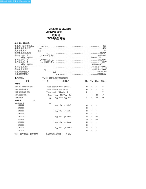
2N3906中文资料(nte)中文数据手册「EasyDatasheet - 矽搜」
VCE = 1V, I C = 1mA
40 − − 80 − −
2N3905 2N3906
VCE = 1V, I C = 10mA
50 − 150 100 − 300
2N3905 2N3906
VCE = 1V, I C = 50mA
30 − − 60 − −
2N3905 2N3906
VCE = 1V, I C = 100mA
芯片中文手册,看全文,戳
2N3905 & 2N3906 硅PNP晶体管
一般用途
TO92类型封装
绝对最大额定值:
集电极 - 发射极电压,V
CEO . . . . . . . . . . . . . . . . . . . . . . . . . . . . . . . . . . . . . . . . . . . . . . . . . . . . . . 40V
器件总功耗(T
C = +255C), PD . . . . . . . . . . . . . . . . . . . . . . . . . . . . . . . . . . . . . . . . . . . . 1.5W
减免上述255℃. . . . . . . . . . . . . . . . . . . . . . . . . . . . . . . . . . . . . . . . . . . . . . . . . . . . . . 12MW / 5C
减免上述255℃. . . . . . . . . . . . . . . . . . . . . . . . . . . . . . . . . . . . . . . 5.0MW / 5C
器件总功耗(T
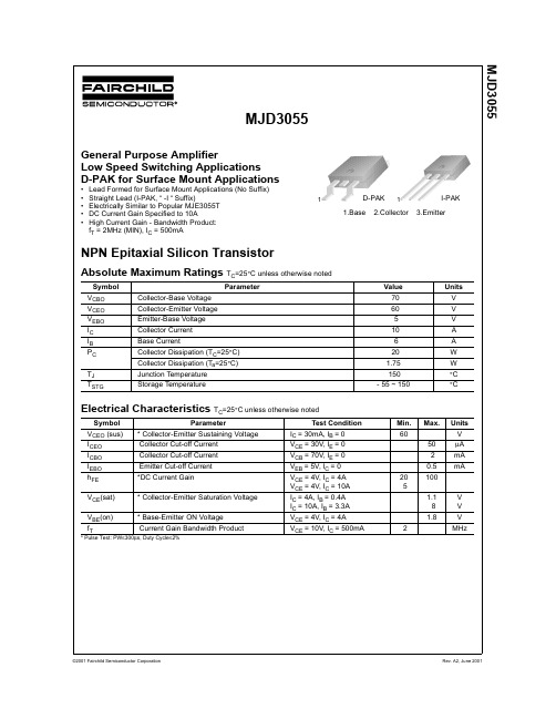
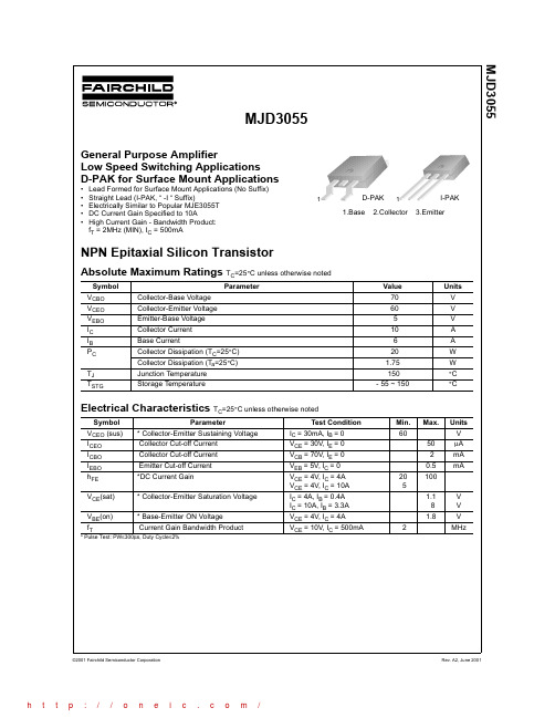
MJD3055中文资料
MJD3055MJD3055MJD3055DISCLAIMERFAIRCHILD SEMICONDUCTOR RESERVES THE RIGHT TO MAKE CHANGES WITHOUT FURTHER NOTICE TO ANY PRODUCTS HEREIN TO IMPROVE RELIABILITY, FUNCTION OR DESIGN. FAIRCHILD DOES NOT ASSUME ANY LIABILITY ARISING OUT OF THE APPLICATION OR USE OF ANY PRODUCT OR CIRCUIT DESCRIBED HEREIN;NEITHER DOES IT CONVEY ANY LICENSE UNDER ITS PATENT RIGHTS, NOR THE RIGHTS OF OTHERS.LIFE SUPPORT POLICYFAIRCHILD’S PRODUCTS ARE NOT AUTHORIZED FOR USE AS CRITICAL COMPONENTS IN LIFE SUPPORT DEVICES OR SYSTEMS WITHOUT THE EXPRESS WRITTEN APPROVAL OF FAIRCHILD SEMICONDUCTOR CORPORATION.As used herein:TRADEMARKSThe following are registered and unregistered trademarks Fairchild Semiconductor owns or is authorized to use and is not intended to be an exhaustive list of all such trademarks.1. Life support devices or systems are devices or systems which, (a) are intended for surgical implant into the body,or (b) support or sustain life, or (c) whose failure to performwhen properly used in accordance with instructions for useprovided in the labeling, can be reasonably expected to result in significant injury to the user.2. A critical component is any component of a life support device or system whose failure to perform can bereasonably expected to cause the failure of the life support device or system, or to affect its safety or effectiveness.PRODUCT STATUS DEFINITIONS Definition of TermsDatasheet Identification Product Status DefinitionAdvance InformationFormative or In Design This datasheet contains the design specifications for product development. Specifications may change in any manner without notice.PreliminaryFirst ProductionThis datasheet contains preliminary data, andsupplementary data will be published at a later date.Fairchild Semiconductor reserves the right to make changes at any time without notice in order to improve design.No Identification Needed Full ProductionThis datasheet contains final specifications. Fairchild Semiconductor reserves the right to make changes at any time without notice in order to improve design.Obsolete Not In ProductionThis datasheet contains specifications on a product that has been discontinued by Fairchild semiconductor.The datasheet is printed for reference information only.A CEx™Bottomless™CoolFET™CROSSVOLT ™DenseTrench™DOME™EcoSPARK™E 2CMOS™EnSigna™FACT™FACT Quiet Series™FAST ®FASTr™FRFET™GlobalOptoisolator™GTO™HiSeC™ISOPLANAR™LittleFET™MicroFET™MICROWIRE™OPTOLOGIC™OPTOPLANAR™PACMAN™POP™Power247™PowerTrench ®QFET™QS™QT Optoelectronics™Quiet Series™SLIENT SWITCHER ®SMART START™STAR*POWER™Stealth™SuperSOT™-3SuperSOT™-6SuperSOT™-8SyncFET™TruTranslation™TinyLogic™UHC™UltraFET ®VCX™STAR*POWER is used under license。
MTP3055E场效应管芯片参数资料(免费)
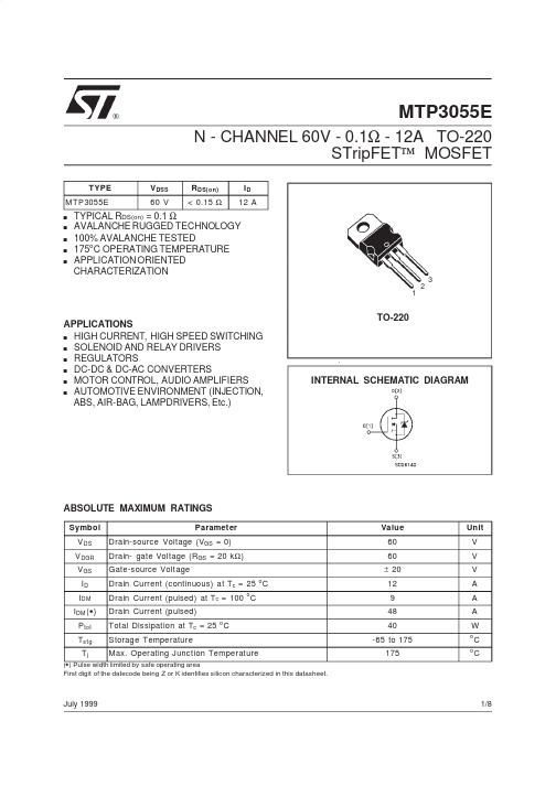
MTP3055EN -CHANNEL 60V -0.1Ω-12A TO-220STripFET ™MOSFETs TYPICAL R DS(on)=0.1Ωs AVALANCHE RUGGED TECHNOLOGY s 100%AVALANCHE TESTEDs 175o C OPERATING TEMPERATURE sAPPLICATION ORIENTED CHARACTERIZATIONAPPLICATIONSs HIGH CURRENT,HIGH SPEED SWITCHING s SOLENOID AND RELAY DRIVERS s REGULATORSs DC-DC &DC-AC CONVERTERSs MOTOR CONTROL,AUDIO AMPLIFIERS s AUTOMOTIVE ENVIRONMENT (INJECTION,ABS,AIR-BAG,LAMPDRIVERS,Etc.)®INTERNAL SCHEMATIC DIAGRAMJuly 1999123TO-220ABSOLUTE MAXIMUM RATINGSSymbol ParameterValue Unit V DS Drain-source Voltage (V GS =0)60V V DGR Drain-gate Voltage (R GS =20k Ω)60V V GS Gate-source Voltage±20V I D Drain Current (continuous)at T c =25o C 12A I DM Drain Current (pulsed)at T c =100oC 9A I DM (•)Drain Current (pulsed)48A P tot Total Dissipation at T c =25o C 40WT s tg Storage Temperature-65to 175o C T jMax.Operating Junction Temperature175oC(•)Pulse width limited by safe operating areaFirst digit of the datecode being Z or K identifies silicon characterized in this datasheet.TYPE V DSS R DS(on)I D MTP3055E60V<0.15Ω12A1/8THERMAL DATAR thj-case R thj-amb R t hc-sT l Thermal Resistance Junction-case MaxThermal Resistance Junction-ambient MaxThermal Resistance Case-sink TypMaximum Lead Temperature For Soldering Purpose3.7562.50.5300o C/WoC/Wo C/Wo CAVALANCHE CHARACTERISTICSSymbol Parameter Max Value UnitI AR Avalanche Current,Repetitive or Not-Repetitive(pulse width limited by T j max)12AE AS Single Pulse Avalanche Energy(starting T j=25o C,I D=I AR,V DD=25V)50mJELECTRICAL CHARACTERISTICS(T case=25o C unless otherwise specified)OFFSymbol Parameter Test Conditions Min.Typ.Max.Unit V(BR)DSS Drain-sourceBreakdown VoltageI D=250µA V GS=060VI DSS Zero Gate VoltageDrain Current(V GS=0)V DS=Max RatingV DS=Max Rating x0.8T c=125o C110µAµAI GSS Gate-body LeakageCurrent(V DS=0)V GS=±20V±100nA ON(∗)Symbol Parameter Test Conditions Min.Typ.Max.Unit V GS(th)Gate Threshold Voltage V DS=V GS I D=250µA2 2.94V R DS(on)Static Drain-source OnResistanceV GS=10V I D=7A0.10.15ΩI D(o n)On State Drain Current V DS>I D(o n)x R DS(on)ma x V GS=10V12A DYNAMICSymbol Parameter Test Conditions Min.Typ.Max.Unitg f s(∗)ForwardTransconductanceV DS>I D(o n)x R DS(on)ma x I D=6A46SC iss C os s C rss Input CapacitanceOutput CapacitanceReverse TransferCapacitanceV DS=25V f=1MHz V GS=076010030pFpFpFMTP3055E 2/8ELECTRICAL CHARACTERISTICS(continued)SWITCHING RESISTIVE LOADSymbol Parameter Test Conditions Min.Typ.Max.Unitt d(on) t r t d(of f) t f Turn-on TimeRise TimeTurn-off Delay TimeFall TimeV DD=30V I D=7AR G=50 ΩV GS=10V(see test circuit)20657035nsnsnsnsQ g Q gs Q gd Total Gate ChargeGate-Source ChargeGate-Drain ChargeI D=12A V GS=10VV DD=40V(see test circuit)1575nCnCnCSOURCE DRAIN DIODESymbol Parameter Test Conditions Min.Typ.Max.UnitI SD I SDM(•)Source-drain CurrentSource-drain Current(pulsed)1248AAV SD(∗)Forward On Voltage I SD=12A V GS=0 2.0Vt rr Q rr Reverse RecoveryTimeReverse RecoveryChargeI SD=12A di/dt=100A/µsV DD=30V T j=150o C650.17nsµC(∗)Pulsed:Pulse duration=300µs,duty cycle1.5%(•)Pulse width limited by safe operating areaSafe Operating Area Thermal ImpedanceMTP3055E3/8Output Characteristics TransconductanceGate Charge vs Gate-source Voltage Transfer CharacteristicsStatic Drain-source On Resistance Capacitance VariationsMTP3055E 4/8Normalized Gate Threshold Voltage vs TemperatureSource-drain Diode Forward Characteristics Normalized On Resistance vs TemperatureMTP3055E5/8Fig.1:Unclamped Inductive Load Test Circuit Fig.3:Switching Times Test Circuits For Resistive Load Fig.2:Unclamped Inductive Waveform Fig.4:Gate Charge test CircuitFig.5:Test Circuit For Inductive Load Switching And Diode Recovery TimesMTP3055E6/8DIM.mminch MIN.TYP.MAX.MIN.TYP.MAX.A 4.40 4.600.1730.181C 1.23 1.320.0480.051D 2.402.720.0940.107D1 1.270.050E 0.490.700.0190.027F 0.610.880.0240.034F1 1.14 1.700.0440.067F2 1.14 1.700.0440.067G 4.95 5.150.1940.203G1 2.4 2.70.0940.106H210.010.400.3930.409L216.40.645L413.014.00.5110.551L5 2.65 2.950.1040.116L615.2515.750.6000.620L7 6.2 6.60.2440.260L9 3.5 3.930.1370.154DIA.3.75 3.850.1470.151L6ACDED 1FGL7L2Dia.F 1L5L4H 2L9F 2G 1TO-220MECHANICAL DATAP011CMTP3055E7/8Information furnished is believed to be accurate and reliable.However,STMicroelect r onics assumes no responsibility for the consequences of use of such information nor for any infringement of patents or other rights of third part i es which may result from its use.No license is granted by implication or otherwise under any patent or patent rights of STMicroelectro nics.Specification mentioned in this publication are subject to change without notice.This publication supersedes and replaces all informat i on previously supplied.STMicroelectronics products are not authorized for use as critical components in life support devices or systems with out express written approval of STMicroelectronics.The ST logo is a trademark of STMicroelectronics©1999STMicroelectronics –Printed in Italy –All Rights ReservedSTMicroelectronics GROUP OF COMPANIESAustralia -Brazil -China -Finland -France -Germany -Hong Kong -India -Italy -Japa n -Malaysia -Malta -Morocco -Singapore -Spain -Sweden -Switzerland -United Kingdom -U.S.A..MTP3055E8/8。
P3055LDG中文资料
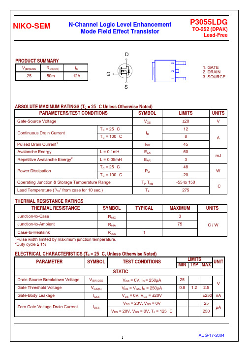
SYMBOL VGS
LIMITS ±20 12S V
TC = 25 °C TC = 100 °C
ID IDM
A
L = 0.1mH L = 0.05mH TC = 25 °C TC = 100 °C
EAS EAR PD Tj, Tstg TL
NIKO-SEM
N-Channel Logic Level Enhancement Mode Field Effect Transistor
P3055LDG
TO-252 (DPAK) Lead-Free
TO-252 (DPAK) MECHANICAL DATA
mm Dimension Min. A B C D E F G 9.35 2.2 0.45 0.89 0.45 0.03 5.2 Typ. Max. 10.4 2.4 0.6 1.5 0.69 0.23 6.2 H I J K L M N Dimension Min. 0.89 6.35 5.2 0.6 0.5 3.96 4.57 Typ. Max. 2.03 6.80 5.5 1 0.9 5.18 mm
mJ
W
Operating Junction & Storage Temperature Range Lead Temperature ( /16” from case for 10 sec.) THERMAL RESISTANCE RATINGS THERMAL RESISTANCE Junction-to-Case Junction-to-Ambient Case-to-Heatsink
2 2 2
Ciss Coss Crss Qg Qgs Qgd td(on) tr td(off) tf VDS = 15V, RL = 1 ID ≅ 12A, VGS = 10V, RGS = 2.5 VDS = 0.5V(BR)DSS, VGS = 10V, ID = 6A VGS = 0V, VDS = 15V, f = 1MHz
MJD3055三极管
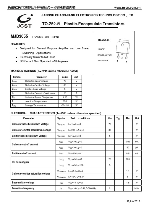
JIANGSU CHANGJIANG ELECTRONICS TECHNOLOGY CO., LTDTO-252-2L Plastic-Encapsulate TransistorsMJD3055 TRANSISTOR (NPN) FEATURES z Designed for General Purpose Amplifier and Low Speed Switching Applications z Electrically Simiar to MJE3055 z DC Current Gain Specified to10 AmperesMAXIMUM RATINGS (T a =25℃ unless otherwise noted)ELECTRICAL CHARACTERISTICS (T a =25℃ unless otherwise specified) ParameterSymbol Test conditions M in T yp M ax U nit Collector-base breakdown voltageV (BR)CBO Ic=1mA,I E =0 70 V Collector-emitter breakdown voltageV (BR)CEO Ic=200 mA,I B =0 60 V Emitter-base breakdown voltage V (BR)EBOI E =1mA,I C =0 5 V I CBOV CB =70V,I E =0 0.02 mA Collector cut-off currentI CEOV CB =30V,I B =0 50 µA Emitter cut-off current I EBOV EB =5V,I C =0 0.5 mA h FE(1)V CE =4V,I C =4A 20 100 DC current gainh FE(2)V CE =4V,I C =10A 5 V CE(sat)(1)I C =4A, I B =0.4A 1.1 V Collector-emitter saturation voltageV CE(sat)(2)I C =10A, I B =3.3A 8 V Base-emitter voltageV BE V CE =4V, I C =4A 1.8 V Transition frequency f T V CE =10V,I C =0.5A,f=500KH Z 2 MHzB,Jun,2012【南京南山半导体有限公司 — 长电三极管选型资料】025507510012515011011010010001234560.10.00.40.81.21.6h —— I AMBIENT TEMPERATURE T a ()℃ 0.5CA P A C I T AN C E C (pF )REVERSE VOLTAGE V (V) Static CharacteristicC O L L E C T O R C U R R E N T I C(A )101CO L L E C T O R C U R R E N T I C(A )MJD3055Typical Characteristics CO L L E C T O R -E M I T T E R S A T U R A T I O N VOLTA GEV C E sat(V )B,Jun,2012 【南京南山半导体有限公司 — 长电三极管选型资料】Inner Box: 340 mm×336mm×29mm Outer Box: 353 mm× 346mm× 365mmLabel on the Reel Label on the Inner BoxLabel on the Outer BoxQA LabelSeal the boxwith the tapeStamp “EMPTY” on the empty boxLabel on the Inner Box Label on the Outer BoxQA LabelSeal the box with the tape Stamp “EMPTY” on the empty box Blue nail White nail Bubble paperOuter Box: 594 mm × 292mm × 185mm Inner Box: 577 mm ×162mm ×53mmLabel on the Inner Box Label on the Outer Box QA LabelSeal the box with the tape Stamp “EMPTY” on the empty box Blue nail White nailOuter Box: 585 mm × 385mm × 220mm Inner Box: 560 mm ×178mm ×35mm。
L6599中文版
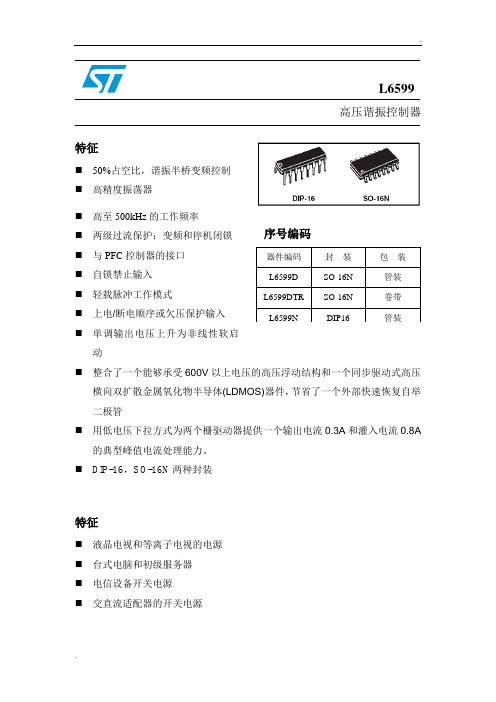
L6599高压谐振控制器特征⏹ 50%占空比,谐振半桥变频控制 ⏹ 高精度振荡器⏹ 高至500kHz 的工作频率 ⏹ 两级过流保护:变频和停机闭锁 ⏹ 与PFC 控制器的接口 ⏹ 自锁禁止输入 ⏹ 轻载脉冲工作模式⏹ 上电/断电顺序或欠压保护输入 ⏹ 单调输出电压上升为非线性软启动⏹ 整合了一个能够承受600V 以上电压的高压浮动结构和一个同步驱动式高压横向双扩散金属氧化物半导体(LDMOS)器件,节省了一个外部快速恢复自举二极管⏹ 用低电压下拉方式为两个栅驱动器提供一个输出电流0.3A 和灌入电流0.8A的典型峰值电流处理能力。
⏹ DIP-16,SO-16N 两种封装特征⏹ 液晶电视和等离子电视的电源 ⏹ 台式电脑和初级服务器 ⏹ 电信设备开关电源 ⏹ 交直流适配器的开关电源序号编码器件编码 封 装 包 装 L6599D SO-16N 管装 L6599DTR SO-16N 卷带 L6599NDIP16管装框图目录1 驱动描述 . . . . . . . . . . . . . . . . . . . . . . . . . . . . . . . . . . . . . . . . . . . . . . . . . .42 引脚设置 . . . . . . . . . . . . . . . . . . . . . . . . . . . . . . . . . . . . . . . . . . . . . . . . . .52.1 引脚排列 . . . . . . . . . . . . . . . . . . . . . . . . . . . . . . . . . . . . . . . . . . . . . . . . . . . .52.2 引脚功能说明 . . . . . . . . . . . . . . . . . . . . . . . . . . . . . . . . . . . . . . . . . . . . . . . . 53 典型系统框图 . . . . . . . . . . . . . . . . . . . . . . . . . . . . . . . . . . . . . . . . . . . . . . 74 电气数据 . . . . . . . . . . . . . . . . . . . . . . . . . . . . . . . . . . . . . . . . . . . . . . . . . . 74.1 极限参数 . . . . . . . . . . . . . . . . . . . . . . . . . . . . . . . . . . . . . . . . . . . . . . . . . . . . . .74.2 热相关数据 . . . . . . . . . . . . . . . . . . . . . . . . . . . . . . . . . . . . . . . . . . . . . . . . . . . . .85 电气参数 . . . . . . . . . . . . . . . . . . . . . . . . . . . . . . . . . . . . . . . . . . . . . . . . . . . 96 典型的电气性能 . . . . . . . . . . . . . . . . . . . . . . . . . . . . . . . . . . . . . . . . . . . . . .127 应用资料 . . . . . . . . . . . . . . . . . . . . . . . . . . . . . . . . . . . . . . . . . . . . . . . . . . . 157.1 振荡器 . . . . . . . . . . . . . . . . . . . . . . . . . . . . . . . . . . . . . . . . . . . . . . . . . . . . . . .167.2 工作在空载或非常轻的负载状态 . . . . . . . . . . . . . . . . . . . . . . . . . . . . . . . . . . .187.3 软启动 . . . . . . . . . . . . . . . . . . . . . . . . . . . . . . . . . . . . . . . . . . . . . . . . . . . . . . . .217.4 电流检测,过流保护和过载保护 . . . . . . . . . . . . . . . . . . . . . . . . . . . . . . . . . 237.5 闭锁关机 . . . . . . . . . . . . . . . . . . . . . . . . . . . . . . . . . . . . . . . . . . . . . . . . . . . . . .267.6 LINE检测功能 . . . . . . . . . . . . . . . . . . . . . . . . . . . . . . . . . . . . . . . . . . . . . . . . . .277.7 自举部分 . . . . . . . . . . . . . . . . . . . . . . . . . . . . . . . . . . . . . . . . . . . . . . . . . . . .287.8 应用实例 . . . . . . . . . . . . . . . . . . . . . . . . . . . . . . . . . . . . . . . . . . . . . . . . . . . . .298 封装外形尺寸 . . . . . . . . . . . . . . . . . . . . . . . . . . . . . . . . . . . . . . . . . . . . . . . . .9 修订记录 . . . . . . . . . . . . . . . . . . . . . . . . . . . . . . . . . . . . . . . . . . . . . . . . . . . .1 驱动描述L6599是一个用于谐振半桥拓扑电路的精确的双端控制器。
3055_精品文档
3055简介:3055是一个广泛应用于电子产品中的NPN功率晶体管,主要用于放大和开关应用。
它具有高频率能力和高电流能力,使其在多个领域中得到广泛使用。
一、基本特性1. 封装类型:TO-220AB、TO-220FP、TO-3PN、SOT-322. 极限电压:集电极-发射极(VCEO)为60V,集电极-基极(VCEV)为60V,发射极-基极(VEBO)为5V3. 最大电流:集电极电流(IC)为10A4. 最大功率:最大耗散功率(PD)为65W5. 高频特性:截止频率(fT)为2.5MHz二、主要应用3055广泛应用于各种电子设备中,包括音频放大器、功率开关和稳压电路等。
以下是该晶体管在一些常见应用中的使用情况:1. 音频放大器3055在音频放大器电路中通常作为功率输出器件。
由于它具有良好的线性特性和高频特性,能够提供较大的音频功率输出。
它经常用于音响系统、家庭影院系统和车载音响系统等。
2. 电源开关3055在电源开关电路中扮演着重要的角色。
它能够通过控制输入信号的变化来实现电源的开关和闭合。
这使得3055在开关电源、UPS(不间断电源)和电动机控制等应用中广泛使用。
3. 稳压电路3055也常被用于稳压电路中,用来控制输出电压的稳定性。
通过正确的设计和配置,可以实现稳定的输出电压,并保护其他电子元件不受过高或过低的电压影响。
4. RF功率放大器由于3055具有较高的频率特性,因此它也可以用作射频功率放大器中的驱动器等。
它能够根据输入信号的变化来放大射频信号,并在射频系统中提供所需的功率。
三、性能参数1. 饱和压降:集电极-发射极饱和压降(VCEsat)为1.1V(最大)2. 硬开关时间:开关时间(Ton, Toff)为1.0μs(最小)3. 热阻:封装的热阻(Junction-to-case thermal resistance)为1.8°C/W(最大)4. 输入电容:输入电容(Cib)为45pF(典型值)四、元件选型和替代型号在选择3055晶体管时,您应该考虑以下因素:1. 特性匹配:根据您所需的应用要求,选择与3055相匹配的特性。
UITRODE公司 U-165 反激式转换器参考设计说明书
UITRODE 公司U-165Lisa DinwoodieReference Design:Isolated 50 Watt Flyback Converter Usingthe UCC3809 Primary Side Controller参考设计:采用UCC3809初级侧控制器的隔离型50W 反激式转换器应用笔记U-165 —— ZHCU009 —— 2001年6月Lisa DinwoodieUITRODE公司U-165-165参考设计:采用UCC3809初级侧控制器的隔离型50W反激式转换器作者:Lisa Dinwoodie摘要对于功率等级为150W(或更低)的单输出或多输出DC-DC转换器而言,反激式功率级是一种普遍的选择。
由于它不像降压型拓扑结构(比如:正激式或推挽式转换器)那样需要使用输出电感器,因此缩减了元件数目和成本。
本应用笔记将评述反激式转换器的功率级和控制电子线路的设计程序。
在这些隔离型转换器中,来自次级侧的误差信号仍需穿越隔离边界以实现稳压。
通过在次级侧上使用具低失调误差放大器的UC3965精密基准(以驱动一个光耦合器)、并在初级侧上采用UCC3809经济型初级侧控制器,实现了一款简单和低成本的50W隔离型电源。
引言本应用笔记所评述的反激式转换器专为与电信行业中所使用的电压范围相对接而设计。
这款5V、50W电源的主要目标是造就一种能够在保持低成本的同时满足所有规格要求的高效设计方案。
该目标是通过在初级侧上使用UCC3809(以提供固定频率电流模式控制)、并在次级侧上采用UC3965的误差放大器和精密基准来实现的。
这些8引脚集成电路均只需极少的外部元件,从而实现了一种经济而有效的设计。
其原理图示于图1中,而材料清单列表于第16页。
1UITRODE 公司U-165U-165APPLICATION NOTED 51N 5819F D Figure 1.Schematic diagram of the –48V to +5V flyback converter.图1:-48V至+5V 反激式转换器的原理示意图2UITRODE 公司U-165-165U-165APPLICATION NOTE3UITRODE公司U-165U-165APPLICATION NOTETheDC transfer function of a CCM flyback con-verter is:V V V V N D D O D IN Rds on +=× (min)()max max ––11(1)where V O equals the output voltage, 5V ,V D =forward voltage drop across rectifier D1,as-sumed to be 0.8V ,V IN = 32 to 72V , V IN(min)= 32V ,V Rds(on)=on voltage drop across MOSFET Q1,equal to R ds(on)x I (primary), assumed to be 1V ,N = turns ratio, equal to N P /N S ,N S = number of transformer secondary turns,N P = number of transformer primary turns,D = duty cycle.Maximum duty cycle,0.45,occurs at minimum in-put voltage.Substituting these values into (1)gives us a turns ratio of 4.66.The turns ratio is inversely proportional to the peak primary current,I PEAK ,but directly proportional to the voltage stress on the switching element.So the peak currents will not become unreasonably high and the voltage stress on the MOSFET will be kept as low as possible,the turns ratio is rounded up only to the next inte-ger value,5,or simply five primary turns for every one secondary turn.Recalculating equation (1)re-sults in an actual D maxof 48%.Switching Frequency Because the magnetic components and filters will be smaller,the tendency is to have as high a switching frequency as possible.Unfortunately,the decision is not quite that clear cut.Core losses,gate charge currents,and switching losses in-crease with higher switching frequencies;peak cur-rents increase with lower switching frequencies.A compromise must be reached between component size,current levels,and acceptable losses.Syn-chronization with other systems and backward compatibility may also be deciding factors.For this design,a fixed frequency (f sw )of 70kHz was cho-sen.At D max equal to 48%,t on(max)becomes 6.9µs.Transformer Design [2]The transformer in a flyback converter is actually a coupled inductor with multiple windings.Trans-formers provide coupling and isolation whereas inductors provide energy storage.The energystored in the air gap of the inductor is equal to:()E L I P PEAK =×22(2)where E is in Joules,L P is the primary inductance in Henries,and I PEAK is the peak primary current in Amperes.When the switch is on,D1(from Figure 2)is reverse biased due to the dot configuration of the transformer.No current flows in the secondary windings and the current in the primary winding ramps up at a rate of:∆∆I t V V L L IN Rds P =(min)(–on)(3)where V IN(min)and V Rds(on)were defined previously and ∆t is equal to t on(max )at V IN(min).The output capacitor,C OUT ,supplies all of the load current at this time.Because the converter is operating in the continuous conduction mode,∆I L is the change in the inductor current which appears as a positive slope ramp on a step.The step is present because there is still current left in the secondary windings when the primary turns on.When the switch turns off,current flows through the secondary winding and D1as a negative ramp on a step,replenishing C OUT and supplying current directly to the load.Based on (3),the primary inductance can be calcu-lated given an acceptable current ripple,I L .For this design,I L was set to equal one-half the peak primary current.For a CCM flyback design,the peak primary current is calculated based upon (4).()I I N D I PEAK OUT L = × +max max –112∆(4)By replacing PEAK ),I OUT(max)with 10A,D max with with 5as detailed earlier,the peak primary current is calculated to be 5.16A and I L calculates to 2.58A.The root mean square,current CCM DC 式中,V O 等于输出电压 (5V),V D = 整流器D1两端的正向压降,假设为0.8V ,V IN = 32V 至72V ,V IN(min) = 32V ,V Rds(on) = MOSFET Q1两端的导通压降,等于R DS(on)×I (primary),假设为1V ,N = 匝数比,等于N P / N S ,N S = 变压器次级匝数,N P = 变压器初级匝数,D = 占空比。
AO4459中文资料

AO4459中⽂资料SymbolTyp Max 33406275R θJL 1824Maximum Junction-to-Lead CSteady-State°C/WThermal Characteristics ParameterUnits Maximum Junction-to-AmbientAt ≤ 10s R θJA °C/W Maximum Junction-to-Ambient ASteady-State °C/W AO4459AO4459SymbolMin TypMaxUnits BV DSS -30V -1T J =55°C-5I GSS ±100nA V GS(th)-1.5-1.85-2.5V I D(ON)-30A 3846T J =125°C53685872m ?g FS 11S V SD -0.78-1V I S-3.5A C iss 668830pF C oss 126pF C rss 92pF R g69?Q g (10V)12.716nC Q g (4.5V) 6.4nC Q gs 2nC Q gd 4nC t D(on)7.7ns t r 6.8ns t D(off)20ns t f 10ns t rr 2230ns Q rr15nCTHIS PRODUCT HAS BEEN DESIGNED AND QUALIFIED FOR THE CONSUMER MARKET. APPLICATIONS OR USES AS CRITICAL COMPONENTS IN LIFE SUPPORT DEVICES OR SYSTEMS ARE NOT AUTHORIZED. AOS DOES NOT ASSUME ANY LIABILITY ARISING OUT OF SUCH APPLICATIONS OR USES OF ITS PRODUCTS. AOS RESERVES THE RIGHT TO IMPROVE PRODUCT DESIGN,FUNCTIONS AND RELIABILITY WITHOUT NOTICE.DYNAMIC PARAMETERS Maximum Body-Diode Continuous CurrentGate resistanceV GS =0V, V DS =0V, f=1MHzV GS =0V, V DS =-15V, f=1MHz Input Capacitance Output Capacitance Turn-On Rise Time Turn-Off DelayTime V GS =-10V, V DS =-15V, R L =2.5?, R GEN =3?Turn-Off Fall TimeTurn-On DelayTime SWITCHING PARAMETERSTotal Gate Charge (4.5V)Gate Source Charge Gate Drain Charge Total Gate Charge (10V)V GS =-10V, V DS =-15V, I D =-6.5Am ?V GS =-4.5V, I D =-5AI S =-1A,V GS =0V V DS =-5V, I D =-6.5AR DS(ON)Static Drain-Source On-ResistanceForward TransconductanceDiode Forward VoltageI DSS µA Gate Threshold Voltage V DS =V GS I D =-250µA V DS =-24V, V GS =0VV DS =0V, V GS =±20V Zero Gate Voltage Drain Current Gate-Body leakage current Electrical Characteristics (T J =25°C unless otherwise noted)STATIC PARAMETERS ParameterConditions Body Diode Reverse Recovery Time Body Diode Reverse Recovery ChargeI F =-6.5A, dI/dt=100A/µsDrain-Source Breakdown Voltage On state drain currentI D =-250µA, V GS =0V V GS =-10V, V DS =-5V V GS =-10V, I D =-6.5AReverse Transfer Capacitance I F =-6.5A, dI/dt=100A/µs A: The value of R θJA is measured with the device mounted on 1in 2FR-4 board with 2oz. Copper, in a still air environment with T A =25°C. The value in any a given application depends on the user's specific board design. The current rating is based on the t ≤ 10s thermal resistance rating.B: Repetitive rating, pulse width limited by junction temperature.C. The R θJA is the sum of the thermal impedence from junction to lead R θJL and lead to ambient.D. The static characteristics in Figures 1 to 6 are obtained using < 300µs pulses, duty cycle 0.5% max.E. These tests are performed with the device mounted on 1 in 2FR-4 board with 2oz. Copper, in a still air environment with T A =25°C. The SOA curve provides a single pulse rating. Rev0 Sept 2006AO4459AO4459。
MJD2955G;MJD2955T4G;MJD3055T4G;MJD2955T4;MJD3055T4;中文规格书,Datasheet资料
THERMAL CHARACTERISTICS
Characteristic Thermal Resistance, Junction−to−Case Thermal Resistance, Junction−to−Ambient (Note 2) Symbol RqJC RqJA Max 6.25 71.4 Unit C/W C/W
MAXIMUM RATINGS
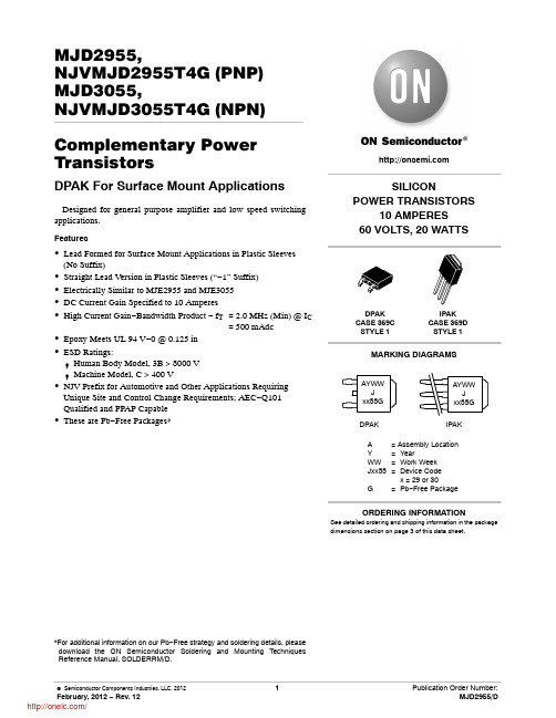
Rating Collector−Emitter Voltage Collector−Base Voltage Emitter−Base Voltage Collector Current Base Current Total Power Dissipation @ TC = 25C Derate above 25C Total Power Dissipation (Note 1) @ TA = 25C Derate above 25C Operating and Storage Junction Temperature Range Symbol VCEO VCB VEB IC IB PD{ Max 60 70 5 10 6 20 0.16 1.75 0.014 − 55 to +150 Unit Vdc Vdc Vdc Adc Adc W W/C W W/C C
Features
SILICON POWER TRANSISTORS 10 AMPERES 60 VOLTS, 20 WATTS
Lead Formed for Surface Mount Applications in Plastic Sleeves
ORDERING INFORMATION
Device MJD2955G MJD2955−1G MJD2955T4G NJVMJD2955T4G MJD3055G MJD3055T4G NJVMJD3055T4G Package Type DPAK (Pb−Free) IPAK (Pb−Free) DPAK (Pb−Free) DPAK (Pb−Free) DPAK (Pb−Free) DPAK (Pb−Free) DPAK (Pb−Free) Package 369C 369D 369C 369C 369C 369C 369C Shipping† 75 Units / Rail 75 Units / Rail 2,500 Tape & Reel 2,500 Tape & Reel 75 Units / Rail 2,500 Tape & Reel 2,500 Tape & Reel
CD4094中文资料
*4094 与74ls164 的编程使用区别,仅仅在于多了一个1脚锁存端口。
当1脚为高电平时,其使用方法与164一模一样。
各位老师可以在以前164驱动的程序里,直接将加入将1脚置为高电平即可。
**另外,当1脚为低电平时,其输出引脚被锁定,Q引脚输出数据不会变化。
**但当锁存(1脚为低电平时),你跟4094通讯,可以使其内部数据改变,改变后,将1脚置为高电平,其Q输出引脚会被立即更新。
CD4094 位移位存储总线寄存器: CD4094是带输出锁存和三态控制的串入/并出高速转换器,具有使用简单、功耗低、驱动能力强和控制灵活等优点。
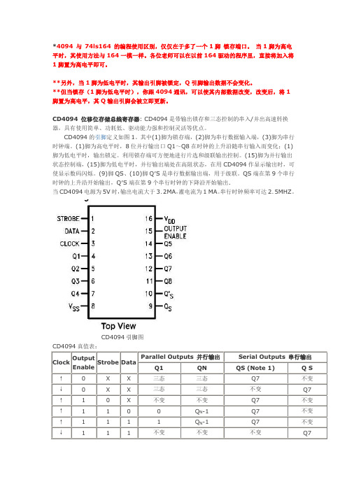
CD4094的引脚定义如图1。
其中(1)脚为锁存端,(2)脚为串行数据输入端,(3)脚为串行时钟端。
(1)脚为高电平时,8位并行输出口Q1~Q8在时钟的上升沿随串行输入而变化;(1)脚为低电平时,输出锁定。
利用锁存端可方便地进行片选和级联输出控制。
(15)脚为并行输出状态控制端,(15)脚为低电平时,并行输出端处在高阻状态,在用CD4094作显示输出时,可使显示数码闪烁。
(9)脚QS、(10)脚Q′S是串行数据输出端,用于级联。
QS端在第9个串行时钟的上升沿开始输出,Q′S端在第9个串行时钟的下降沿开始输出.当CD4094电源为5V时,输出电流大于3.2MA,灌电流为1 MA。
串行时钟频率可达2.5MHZ。
CD4094引脚图CD4094真值表:Clock OutputEnableStrobe DataParallel Outputs 并行输出Serial Outputs 串行输出Q1 QN QS (Note 1) Q S↑0 X X 三态三态Q7 不变↓0 X X 三态三态不变Q7 ↑ 1 0 X 不变不变Q7 不变↑ 1 1 0 0 Q N-1 Q7 不变↑ 1 1 1 1 Q N-1 Q7 不变↓ 1 1 1 不变不变不变Q7CD4094内部电路方框图Absolute Maximum Ratings 绝对最大额定值:Supply Voltage电源电压(VDD) -0.5 to +18 VDCInput Voltage输入电压(VIN) 838电子-0.5 to VDD +0.5 VDCStorage Temperature Range储存温度范围(TS) -65℃to +150℃Power Dissipation功耗(PD)Dual-In-Line 普通双列封装新艺图库700 mWSmall Outline 小外形封装500 mWLead Temperature 焊接温度(TL)Soldering, 10 seconds)(焊接10秒)260℃Recommended Operating Conditions 建议操作条件:DC Supply Voltage 直流供电电压(VDD) +3.0 to +15 VDC Input Voltage输入电压(VIN) 838电子0 to VDD VDC Operating Temperature Range工作温度范围(TA) -40℃to +85℃DC Electrical Characteristics 直流电气特性:Symbol 符号Parameter参数Conditions 条件-40°C +25°C +85°C Units单位最小最大最小典型最大最小最大IDD QuiescentDeviceCurrent静态电流VDD = 5.0V 20 20 150μA VDD = 10V 40 40 300VDD = 15V 80 80 600VOL LOW LevelOutputVDD=5.0V|IO|≤1.μA0.05 0 0.05 0.05V VDD=10V 0.05 0 0.05 0.05Voltage 输出低电平电压VDD=15V0.050.050.05VOHHIGH Level OutputVoltage 输出高电平电压VDD=5.0V|IO|≤1μA 4.954.955.0 4.95 VVDD=10V 9.959.95 10.0 9.95VDD=15V14.9514.95 15.014.95VILLOW Level InputVoltage 输入低电平电压VDD = 5.0V, VO =0.5V or 4.5V 1.5 1.5 1.5 V VDD = 10V, VO =1.0V or 9.0V3.0 3.0 3.0 VDD = 15V, VO = 1.5V or 13.5V 838电子4.04.0 4.0VIHHIGH Level InputVoltage 输入高电平电压VDD = 5.0V, VO = 0.5V or 4.5V 3.5 3.5 3.5 VVDD = 10V, VO = 1.0V or 9.0V7.0 7.07.0 VDD = 15V, VO = 1.5V or 13.5V11.011.011.0 IOLLOW Level OutputCurrent 输出低电平电流 (Note 4)VDD=5.0V,VO=0.4V 0.52 0.44 0.88 0.36 mAVDD=10V,VO=0.5V 1.31.12.25 0.9VDD=15V,VO=1.5V 3.6 3.08.82.4 IOHHIGH Level OutputCurrent 输出高电平电流 (Note 4)VDD=5.0V,VO =4.6V -0.52 -0.44 0.88 -0.36 mAVDD =10V,VO= 9.5V -1.3-1.1 2.25-0.9VDD=15V,VO =13.5V -3.6 -3.0 8.8-2.4IINInputCurrent 输入电流 VDD =15V,VIN =0V -0.3 -0.3 -1.0 μA VDD=15V,VIN =15V0.30.31.0IOZ3-STATE OutputLeakage Current 3态输出漏电流VDD=15V,VIN=0V or 15V1110μAAC Electrical Characteristics 交流电气特性: Symbol符号Parameter 参数 838电子Conditions条件最小 典型 最大Units 单位tPHL, tPLH Propagation Delay Clock to QSVDD = 5.0V 300 600nsVDD = 10V 125 250VDD = 15V 95 190tPHL, tPLH Propagation Delay Clock to Q¢ SVDD =5.0V230 460nsVDD = 10V110 220VDD = 15V 75 150 nstPHL, tPLH Propagation Delay Clock to Parallel OutVDD = 5.0V 420 840nsVDD = 10V 195 390VDD = 15V 135 270tPHL, tPLH Propagation Delay Strobe to Parallel OutVDD = 5.0V 290 580nsVDD = 10V 145 290VDD = 15V 100 200tPHZ Propagation Delay HIGH Level to HIGHImpedanceVDD = 5.0V 140 280nsVDD = 10V 75 150VDD = 15V 55 110tPLZ Propagation Delay LOW Level to HIGHImpedanceVDD = 5.0V 140 280nsVDD = 10V 75 150VDD = 15V 55 110tPZH Propagation Delay HIGH Impedance to HIGHLevelVDD = 5.0V 140 280nsVDD = 10V 75 150VDD = 15V 55 110tPZL Propagation Delay HIGH Impedance to LOWLevelVDD = 5.0V 140 280nsVDD = 10V 75 150VDD = 15V 55 110tTHL, tTLH Transition Time过渡时间VDD = 5.0V 100 200nsVDD = 10V 50 100VDD = 15V 40 80tSU Set-Up Time Data to Clock 建立时间数据时钟VDD = 5.0V 80 40ns VDD = 10V 40 20VDD = 15V 20 10tr, tf Maximum Clock Rise and Fall Time最大时钟上升和下降时间VDD = 5.0V 1msVDD = 10V 1VDD = 15V 1tPC Minimum Clock Pulse Width最小时钟脉冲宽度VDD = 5.0V 200 100ns VDD = 10V 100 50VDD = 15V 83 40tPSMinimum Strobe Pulse WidthVDD = 5.0V 200 100nsVDD = 10V 80 40 VDD = 15V 70 35fmaxMaximum Clock Frequency 最大时钟频率VDD = 5.0V 1.5 3.0MHzVDD = 10V 3.0 6.0 VDD = 15V 4.0 8.0CINInput Capacitance 输入电容 Any Input 5.0 7.5 pF测试电路和3态时序图。
MJD3055TF;中文规格书,Datasheet资料
MJD3055MJD3055MJD3055DISCLAIMERFAIRCHILD SEMICONDUCTOR RESERVES THE RIGHT TO MAKE CHANGES WITHOUT FURTHER NOTICE TO ANY PRODUCTS HEREIN TO IMPROVE RELIABILITY, FUNCTION OR DESIGN. FAIRCHILD DOES NOT ASSUME ANY LIABILITY ARISING OUT OF THE APPLICATION OR USE OF ANY PRODUCT OR CIRCUIT DESCRIBED HEREIN;NEITHER DOES IT CONVEY ANY LICENSE UNDER ITS PATENT RIGHTS, NOR THE RIGHTS OF OTHERS.LIFE SUPPORT POLICYFAIRCHILD’S PRODUCTS ARE NOT AUTHORIZED FOR USE AS CRITICAL COMPONENTS IN LIFE SUPPORT DEVICES OR SYSTEMS WITHOUT THE EXPRESS WRITTEN APPROVAL OF FAIRCHILD SEMICONDUCTOR CORPORATION.As used herein:TRADEMARKSThe following are registered and unregistered trademarks Fairchild Semiconductor owns or is authorized to use and is not intended to be an exhaustive list of all such trademarks.1. Life support devices or systems are devices or systems which, (a) are intended for surgical implant into the body,or (b) support or sustain life, or (c) whose failure to performwhen properly used in accordance with instructions for useprovided in the labeling, can be reasonably expected to result in significant injury to the user.2. A critical component is any component of a life support device or system whose failure to perform can bereasonably expected to cause the failure of the life support device or system, or to affect its safety or effectiveness.PRODUCT STATUS DEFINITIONS Definition of TermsDatasheet Identification Product Status DefinitionAdvance InformationFormative or In Design This datasheet contains the design specifications for product development. Specifications may change in any manner without notice.PreliminaryFirst ProductionThis datasheet contains preliminary data, andsupplementary data will be published at a later date.Fairchild Semiconductor reserves the right to make changes at any time without notice in order to improve design.No Identification Needed Full ProductionThis datasheet contains final specifications. Fairchild Semiconductor reserves the right to make changes at any time without notice in order to improve design.Obsolete Not In ProductionThis datasheet contains specifications on a product that has been discontinued by Fairchild semiconductor.The datasheet is printed for reference information only.A CEx™Bottomless™CoolFET™CROSSVOLT ™DenseTrench™DOME™EcoSPARK™E 2CMOS™EnSigna™FACT™FACT Quiet Series™FAST ®FASTr™FRFET™GlobalOptoisolator™GTO™HiSeC™ISOPLANAR™LittleFET™MicroFET™MICROWIRE™OPTOLOGIC™OPTOPLANAR™PACMAN™POP™Power247™PowerTrench ®QFET™QS™QT Optoelectronics™Quiet Series™SLIENT SWITCHER ®SMART START™STAR*POWER™Stealth™SuperSOT™-3SuperSOT™-6SuperSOT™-8SyncFET™TruTranslation™TinyLogic™UHC™UltraFET ®VCX™STAR*POWER is used under license分销商库存信息: FAIRCHILDMJD3055TF。
2N3055中文资料_数据手册_参数
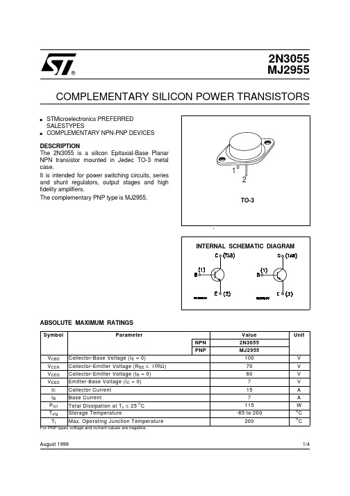
VCEO Collector-Emitter Voltage (IB = 0)
VEBO Emitter-Base Voltage (IC = 0)
IC
Collector Current
IB
Base Current
Ptot Total Dissipation at Tc ≤ 25 oC
Tstg Storage Temperature
MIN. 0.433 0.038 0.059 0.327 0.748 0.421 0.649 0.984 0.157 1.515 1.187
2N3055 / MJ2955
inch TYP.
MAX. 0.516 0.045 0.065 0.351 0.787 0.437 0.677 1.023 0.161 1.547 1.193
For PNP types voltage and current values are negative.
Min. Typ.
60 70
20 5 3 2.87
Max. 1 5 0.7 5
1 3 1.8 70
Unit mA mA mA mA V
V
V V V
MHz A
2/4
DIM.
A B C D E G N P R U V
VCE = 4 A VCE = 4 A
fT
Transition frequency IC = 0.5 A
VCE = 10 V
Is/b∗ Second Breakdown Collector Current
VCE = 40 V
∗ Pulsed: Pulse duration = 300 µs, duty cycle 1.5 %
PHD3055E中文资料
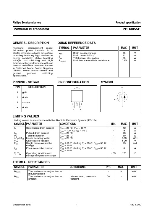
Philips Semiconductors Product specificationPowerMOS transistor PHD3055EGENERAL DESCRIPTIONQUICK REFERENCE DATAN-channel enhancement mode SYMBOL PARAMETERMAX.UNIT field-effect power transistor in a plastic envelope suitable for surface V DS Drain-source voltage 60V mounting featuring high avalanche I D Drain current (DC)12A energy capability,stable blocking P totTotal power dissipation50W voltage,fast switching and high R DS(ON)Drain-source on-state resistance0.15Ωthermal cycling performance with low thermal resistance.Intended for use in Switched Mode Power Supplies (SMPS),motor control circuits and general purpose switching applications.PINNING - SOT428PIN CONFIGURATIONSYMBOLLIMITING VALUESLimiting values in accordance with the Absolute Maximum System (IEC 134)SYMBOL PARAMETER CONDITIONSMIN.MAX.UNIT I DContinuous drain current T mb = 25 ˚C; V GS = 10 V -12A T mb = 100 ˚C; V GS = 10 V -9A I DM Pulsed drain current T mb = 25 ˚C -48A P DTotal dissipationT mb = 25 ˚C -50W ∆P D /∆T mb Linear derating factor T mb > 25 ˚C-0.33W/K V GS Gate-source voltage -± 30V E AS Single pulse avalanche V DD ≤ 50 V; starting T j = 25˚C; R GS = 50 Ω;-25mJ energyV GS = 10 VI AS Peak avalanche current V DD ≤ 50 V; starting T j = 25˚C; R GS = 50 Ω;-6A V GS = 10 VT j , T stgOperating junction and - 55175˚Cstorage temperature rangeTHERMAL RESISTANCESSYMBOL PARAMETERCONDITIONSTYP.MAX.UNIT R th j-mb Thermal resistance junction to -3K/W mounting baseR th j-aThermal resistance junction to pcb mounted, minimum 50-K/WambientfootprintPhilips Semiconductors Product specificationPowerMOS transistor PHD3055EELECTRICAL CHARACTERISTICST j = 25 ˚C unless otherwise specified SYMBOL PARAMETERCONDITIONSMIN.TYP.MAX.UNIT V (BR)DSS Drain-source breakdown V GS = 0 V; I D = 0.25 mA 60--V voltage∆V (BR)DSS /Drain-source breakdownV DS = V GS ; I D = 0.25 mA-0.08-V/K ∆T jvoltage temperature coefficient R DS(ON)Drain-source on resistance V GS = 10 V; I D = 6 A -0.10.15ΩV GS(TO)Gate threshold voltage V DS = V GS ; I D = 0.25 mA 2.0 3.0 4.0V g fs Forward transconductance V DS = 50 V; I D = 6 A 2.4 4.0-S I DSS Drain-source leakage current V DS = 60 V; V GS = 0 V-0.125µA V DS = 48 V; V GS = 0 V; T j = 150 ˚C -1250µA I GSS Gate-source leakage current V GS = ±30 V; V DS = 0 V-10100nA Q g(tot)Total gate charge I D = 10 A; V DD = 48 V; V GS = 10 V -1012nC Q gs Gate-source charge-23nC Q gd Gate-drain (Miller) charge - 5.67nC t d(on)Turn-on delay time V DD = 30 V; I D = 10 A;-8-ns t rTurn-on rise time R G = 24 Ω; R D = 2.7 Ω-55-ns t d(off)Turn-off delay time -25-ns t f Turn-off fall time-22-ns L d Internal drain inductance Measured from tab to centre of die - 3.5-nH L s Internal source inductance Measured from source lead solder -7.5-nH point to source bond pad C iss Input capacitance V GS = 0 V; V DS = 25 V; f = 1 MHz-220-pF C oss Output capacitance -108-pF C rssFeedback capacitance-48-pFSOURCE-DRAIN DIODE RATINGS AND CHARACTERISTICST j = 25 ˚C unless otherwise specified SYMBOL PARAMETERCONDITIONS MIN.TYP.MAX.UNIT I S Continuous source current T mb = 25˚C --12A (body diode)I SM Pulsed source current (body T mb = 25˚C --48A diode)V SD Diode forward voltage I S = 10 A; V GS = 0 V -- 1.5V t rr Reverse recovery time I S = 10 A; V GS = 0 V;-38-ns dI/dt = 100 A/µsQ rrReverse recovery charge-0.1-µCPhilips Semiconductors Product specification PowerMOS transistor PHD3055EPhilips Semiconductors Product specification PowerMOS transistor PHD3055EPhilips Semiconductors Product specification PowerMOS transistor PHD3055EPhilips Semiconductors Product specificationPowerMOS transistor PHD3055EMECHANICAL DATAMOUNTING INSTRUCTIONSNotes1. Observe the general handling precautions for electrostatic-discharge sensitive devices (ESDs) to preventdamage to MOS gate oxide.2. Epoxy meets UL94 V0 at 1/8".Philips Semiconductors Product specification PowerMOS transistor PHD3055EDEFINITIONSData sheet statusObjective specification This data sheet contains target or goal specifications for product development. Preliminary specification This data sheet contains preliminary data; supplementary data may be published later. Product specification This data sheet contains final product specifications.Limiting valuesLimiting values are given in accordance with the Absolute Maximum Rating System (IEC 134). Stress above one or more of the limiting values may cause permanent damage to the device. These are stress ratings only and operation of the device at these or at any other conditions above those given in the Characteristics sections ofthis specification is not implied. Exposure to limiting values for extended periods may affect device reliability. Application informationWhere application information is given, it is advisory and does not form part of the specification.© Philips Electronics N.V. 1998All rights are reserved. Reproduction in whole or in part is prohibited without the prior written consent of the copyright owner.The information presented in this document does not form part of any quotation or contract, it is believed to be accurate and reliable and may be changed without notice. No liability will be accepted by the publisher for any consequence of its use. Publication thereof does not convey nor imply any license under patent or other industrial or intellectual property rights.LIFE SUPPORT APPLICATIONSThese products are not designed for use in life support appliances, devices or systems where malfunction of these products can be reasonably expected to result in personal injury. Philips customers using or selling these products for use in such applications do so at their own risk and agree to fully indemnify Philips for any damages resulting from such improper use or sale.。
2.7W双声道立体音频放大器
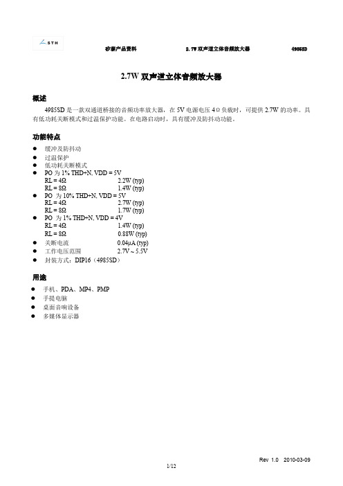
2.7W双声道立体音频放大器概述4985SD是一款双通道桥接的音频功率放大器,在5V电源电压4Ω负载时,可提供2.7W的功率。
具有低功耗关断模式和过温保护功能。
在电路启动时,具有缓冲及防抖动功能。
功能特点l缓冲及防抖动l过温保护l低功耗关断模式l PO为1% THD+N, VDD = 5VRL=4Ω 2.2W(typ)RL=8Ω 1.4W(typ)l PO为10% THD+N, VDD = 5VRL=4Ω 2.7W(typ)RL=8Ω 1.7W(typ)l PO为1% THD+N, VDD = 4VRL=4Ω 1.4W(typ)RL=8Ω0.88W(typ)l关断电流0.04μA(typ)l工作电压范围 2.7V~5.5Vl封装方式:DIP16(4985SD)用途l手机、PDA、MP4、PMPl手提电脑l桌面音响设备l多媒体显示器管脚排列图管脚说明功能框图功能说明桥接参数说明4985SD由两对运算放大器组成双通道(通道A和通道B)立体声放大器。
外接反馈电阻R2,R4和输入电阻R1,R3决定了放大器A(-out)和B(-out)的闭环增益,同时内建20K电阻使放大器A的(+out)和B的(-out)端的增益为1。
4985SD所驱动的负载接在两放大器的输出端-OUTA和+OUTA之间。
放大器A的(-out)端就是放大器A的(+out)端的输入端,这就使两个输出端产生的信号有180°的相位差,利用这个相位差,桥接模式下的增益为:A VD=2*(Rf/Ri)或者A VD=2*(R2/R1)桥接模式比单端模式更有优势。
在桥接模式下,差分输出使增益翻倍,它的输出功率是相同情况下单端模式的4倍。
桥接模式的另一个优势是在负载上没有直流电压。
输出信号由通道A和B偏置在VDD/2。
所以它无需在单端模式下的耦合电容。
在单端输出模式下,如果不使用输出耦合电容,就会在负载上产生一个VDD/2的直流偏置电压,这就会增加芯片的功耗并对负载造成永久性的损害。
3位串并转换led驱动芯片
管脚描述 电源地
串行数据输入 加载信号输入 输出使能输入 串行时钟输入
驱动输出 电源地 驱动输出 驱动输出 串行时钟输出 输出使能输出 加载信号输出 串行数据输出 电源输入
北京中庆微数字设备开发有限公司
4
地址:北京海淀区上地东路 1 号盈创动力园区 E402A
TEL:010-58851581/1582/1590/1591/1592 FAX:010-58851593
2
逻辑框图
ZQL9712S
图 1 功能模块
北京中庆微数字设备开发有限公司
1
地址:北京海淀区上地东路 1 号盈创动力园区 E402A
TEL:010-58851581/1582/1590/1591/1592 FAX:010-58851593
性能参数
图 2 信号时序
ZQL9712S
最大工作范围
参数 供电电压 输入电压 输出电流 输出电压 时钟频率
+0.1
+0.1
+0.1
单位
ns ns ns ns ns ns uA
时序参数
参数 时钟高电平宽度 时钟低电平宽度 信号建立时间 信号保持时间
符号 CLKH CLKL SETUP HOLD
测试条件
最小 25 25 10 10
典型
最大
单位 ns ns ns ns
参数
符号
VDD
T=25。C
T=-40~85。C T=-55~125。C 单位
− VBE
BO
式中,VOH 为驱动输出端输出高电平电压值,VBE 为三极管饱和导通管时发射结电压,IBO 为三
极管饱和导通基极电流。
在 ZQL9712S 多 LED 应用电路中,三极管集电极电阻 RR2、RG2、RB2 阻值计算方法如下:
汽轮机505电调中文手册-1

505/505E,CPC用户手册第一章总则505/505E是以微处理器为基础的调速器,适用于单执行机构或双执行机构的汽轮机控制,505适用于我公司生产的冷凝式汽轮机、背压式汽轮机,505E 适用于我公司生产的抽汽式汽轮机、补汽式汽轮机、抽汽背压式汽轮机。
505/505E调速器具有二种正常操作方式:编程方式和运行方式。
编程方式针对汽轮机具体使用场合选择调速器组态所需的各选项,组态完毕后,运行方式用于汽轮机从启动直至停机的操作。
此外,还能利用服务方式进行在线调整。
§1.1 505/505E的输入505/505E调速器有二个转速输入,转速传感器可以选择磁电式传感器(缺省设臵),也可以选择有源探头(需跳线)。
还有6个可编程模拟量输入。
16个开关量输入,其中4个指定用于停机、复位、升转速给定值和降转速给定值,如果调速器用于驱动发电机的场合,另外有二个开关量输入必须指定用于发电机断路器和电网断路器,其余10个开关量输入都是可组态的;如果调速器不是用于驱动发电机的场合,那么就有12个开关量输入是可组态的。
调速器面板上有4个功能键,F1和F2分别指定用于报警和超速。
F3和F4经组态能投入或退出调速器的各种不同功能。
§1.2 505/505E的输出505/505E调速器有二个带线性化曲线的执行机构输出,8个C型继电器开关量输出,其中6个是可组态的,另二个指定用作停机和报警指示。
§1.3 通讯接口2个Modbus通讯口用作调速器的通讯接口。
采用ASCⅡ或RTU传输协议,通讯可采用RS232,RS-422或RS-485。
第 1 页一个计算机接口用于程序设臵的存储。
第二章安装步骤图2-1所示为标准505/505E调速器的外形和安装型式,调速器装在一个嵌装式壳体中。
这种壳体设计成安装于控制室的屏上或柜子中,其本身无法实现墙挂式安装。
当调速器被正确安装于控制柜中时,其面板后边所附的垫片就将调速器面板密封在柜子上。
- 1、下载文档前请自行甄别文档内容的完整性,平台不提供额外的编辑、内容补充、找答案等附加服务。
- 2、"仅部分预览"的文档,不可在线预览部分如存在完整性等问题,可反馈申请退款(可完整预览的文档不适用该条件!)。
- 3、如文档侵犯您的权益,请联系客服反馈,我们会尽快为您处理(人工客服工作时间:9:00-18:30)。
NTD3055−094Power MOSFET 12 A, 60 VN−Channel DPAKDesigned for low voltage, high speed switching applications in power supplies, converters and power motor controls and bridge circuits.Features•Pb−Free Packages are Available •Lower R DS(on)•Lower V DS(on)•Lower and Tighter V SD•Lower Diode Reverse Recovery Time •Lower Reverse Recovery Stored Charge Typical Applications•Power Supplies •Converters•Power Motor Controls •Bridge CircuitsMAXIMUM RATINGS (T= 25°C unless otherwise noted)Maximum ratings applied to the device are individual stress limit values (not normal operating conditions) and are not valid simultaneously. If these limits are exceeded, device functional operation is not implied, damage may occur and reliability may be affected.1.When surface mounted to an FR4 board using 0.5 sq in. pad size.2.When surface mounted to an FR4 board using the minimum recommended pad size.N−Channel60 V94 m W R DS(on) TYP 12 AI D MAX V (BR)DSS 55094Device CodeA = Assembly Location Y = YearW= Work WeekGate 3Source2Drain 4Drain DPAK CASE 369C STYLE 2MARKING DIAGRAMSGate SourceDrain 4DPAK−3CASE 369D STYLE 2See detailed ordering and shipping information in the package dimensions section on page 7 of this data sheet.ORDERING INFORMATIONA Y W 55094ELECTRICAL CHARACTERISTICS(T= 25°C unless otherwise noted)4.Switching characteristics are independent of operating junction temperatures.I D , D R A I N C U R R E N T (A M P S )R D S (o n ), D R A I N −T O −S O U R C E R E S I S T A N C E (W )Figure 5. On−Resistance Variation withTemperature T J , JUNCTION TEMPERATURE (°C)Figure 6. Drain−to−Source Leakage Currentversus VoltageV DS , DRAIN−TO−SOURCE VOLTAGE (VOLTS)R D S (o n ), D R A I N −T O −S O U R C E R E S I S T A N C E (N O R M A L I Z E D )−505025−2575125100403020601015017550POWER MOSFET SWITCHINGSwitching behavior is most easily modeled and predicted by recognizing that the power MOSFET is charge controlled. The lengths of various switching intervals (D t)are determined by how fast the FET input capacitance can be charged by current from the generator.The published capacitance data is difficult to use for calculating rise and fall because drain−gate capacitance varies greatly with applied voltage. Accordingly, gate charge data is used. In most cases, a satisfactory estimate of average input current (I G(A V)) can be made from a rudimentary analysis of the drive circuit so that t = Q/I G(A V)During the rise and fall time interval when switching a resistive load, V GS remains virtually constant at a level known as the plateau voltage, V SGP . Therefore, rise and fall times may be approximated by the following:t r = Q 2 x R G /(V GG − V GSP )t f = Q 2 x R G /V GSPwhereV GG = the gate drive voltage, which varies from zero to V GG R G = the gate drive resistanceand Q 2 and V GSP are read from the gate charge curve.During the turn−on and turn−off delay times, gate current is not constant. The simplest calculation uses appropriate values from the capacitance curves in a standard equation for voltage change in an RC network. The equations are:t d(on) = R G C iss In [V GG /(V GG − V GSP )]t d(off) = R G C iss In (V GG /V GSP )The capacitance (C iss ) is read from the capacitance curve at a voltage corresponding to the off−state condition when calculating t d(on) and is read at a voltage corresponding to the on−state when calculating t d(off).At high switching speeds, parasitic circuit elements complicate the analysis. The inductance of the MOSFET source lead, inside the package and in the circuit wiring which is common to both the drain and gate current paths,produces a voltage at the source which reduces the gate drive current. The voltage is determined by Ldi/dt, but since di/dt is a function of drain current, the mathematical solution is complex. The MOSFET output capacitance also complicates the mathematics. And finally, MOSFETs have finite internal gate resistance which effectively adds to the resistance of the driving source, but the internal resistance is difficult to measure and, consequently, is not specified.The resistive switching time variation versus gate resistance (Figure 9) shows how typical switching performance is affected by the parasitic circuit elements. If the parasitics were not present, the slope of the curves would maintain a value of unity regardless of the switching speed.The circuit used to obtain the data is constructed to minimize common inductance in the drain and gate circuit loops and is believed readily achievable with board mounted components. Most power electronic loads are inductive; the data in the figure is taken with a resistive load, which approximates an optimally snubbed inductive load. Power MOSFETs may be safely operated into an inductive load;however, snubbing reduces switching losses.GATE−TO−SOURCE OR DRAIN−TO−SOURCE VOLTAGE (VOLTS)C , C A P A C I T A N C E (p F )Figure 7. Capacitance Variation2004006008000.6V SD , SOURCE−TO−DRAIN VOLTAGE (VOLTS)Figure 10. Diode Forward Voltage versus CurrentV G S , G A T E −T O −S O U R C E V O L T A G E (V O L T S )1062840.6810.920.840.76SAFE OPERATING AREAThe Forward Biased Safe Operating Area curves define the maximum simultaneous drain−to−source voltage and drain current that a transistor can handle safely when it is forward biased. Curves are based upon maximum peak junction temperature and a case temperature (T C ) of 25°C.Peak repetitive pulsed power limits are determined by using the thermal response data in conjunction with the procedures discussed in AN569, “Transient Thermal Resistance −General Data and Its Use.”Switching between the off−state and the on−state may traverse any load line provided neither rated peak current (I DM ) nor rated voltage (V DSS ) is exceeded and the transition time (t r ,t f ) do not exceed 10 m s. In addition the total power averaged over a complete switching cycle must not exceed (T J(MAX) − T C )/(R q JC ).A Power MOSFET designated E−FET can be safely used in switching circuits with unclamped inductive loads. Forreliable operation, the stored energy from circuit inductance dissipated in the transistor while in avalanche must be less than the rated limit and adjusted for operating conditions differing from those specified. Although industry practice is to rate in terms of energy, avalanche energy capability is not a constant. The energy rating decreases non−linearly with an increase of peak current in avalanche and peak junction temperature.Although many E−FETs can withstand the stress of drain−to−source avalanche at currents up to rated pulsed current (I DM ), the energy rating is specified at rated continuous current (I D ), in accordance with industry custom.The energy rating must be derated for temperature as shown in the accompanying graph (Figure 12). Maximum energy at currents below rated continuous I D can safely be assumed to equal the values indicated.SAFE OPERATING AREAFigure 11. Maximum Rated Forward BiasedSafe Operating Area T J , STARTING JUNCTION TEMPERATURE (°C)EFigure 12. Maximum Avalanche Energy versusStarting Junction TemperatureV DS , DRAIN−TO−SOURCE VOLTAGE (VOLTS)Figure 13. Thermal Response1100I D , D R A I N C U R R E N T(A M P S )0.110Figure 14. Diode Reverse Recovery WaveformTIMEr (t ), E F F E C T I V E T R A N S I E N T T H E R M A L R E S I S T A N C E (N O R M A L I Z E D )t, TIME (m s)1100.10.010.0010.00010.00001ORDERING INFORMATION†For information on tape and reel specifications, including part orientation and tape sizes, please refer to our Tape and Reel Packaging Specifications Brochure, BRD8011/D.DPAK CASE 369C−01 ISSUE OV SDIM MIN MAX MIN MAXMILLIMETERSINCHESA0.2350.245 5.97 6.22B0.2500.265 6.35 6.73C0.0860.094 2.19 2.38D0.0270.0350.690.88E0.0180.0230.460.58F0.0370.0450.94 1.14G0.180 BSC 4.58 BSCH0.0340.0400.87 1.01J0.0180.0230.460.58K0.1020.114 2.60 2.89L0.090 BSC 2.29 BSCR0.1800.215 4.57 5.45S0.0250.0400.63 1.01U0.020−−−0.51−−−V0.0350.0500.89 1.27Z0.155−−− 3.93−−−STYLE 2:PIN 1.GATE2.DRAIN3.SOURCE4.DRAINǒmmǓSCALE 3:1*For additional information on our Pb−Free strategy and solderingdetails, please download the ON Semiconductor Soldering andMounting Techniques Reference Manual, SOLDERRM/D.SOLDERING FOOTPRINT*DPAK−3CASE 369D−01ISSUE BSTYLE 2:PIN 1.GATE2.DRAIN3.SOURCE4.DRAIN*For additional information on our Pb−Free strategy and solderingdetails, please download the ON Semiconductor Soldering and Mounting Techniques Reference Manual, SOLDERRM/D.SOLDERING FOOTPRINT*ǒmm inchesǓSCALE 3:1E NOTES:1.DIMENSIONING AND TOLERANCING PER ANSI Y14.5M, 1982.2.CONTROLLING DIMENSION: INCH.ON Semiconductor and are registered trademarks of Semiconductor Components Industries, LLC (SCILLC). SCILLC reserves the right to make changes without further notice to any products herein. SCILLC makes no warranty, representation or guarantee regarding the suitability of its products for any particular purpose, nor does SCILLC assume any liability arising out of the application or use of any product or circuit, and specifically disclaims any and all liability, including without limitation special, consequential or incidental damages.“Typical” parameters which may be provided in SCILLC data sheets and/or specifications can and do vary in different applications and actual performance may vary over time. All operating parameters, including “Typicals” must be validated for each customer application by customer’s technical experts. SCILLC does not convey any license under its patent rights nor the rights of others. SCILLC products are not designed, intended, or authorized for use as components in systems intended for surgical implant into the body, or other applications intended to support or sustain life, or for any other application in which the failure of the SCILLC product could create a situation where personal injury or death may occur. Should Buyer purchase or use SCILLC products for any such unintended or unauthorized application, Buyer shall indemnify and hold SCILLC and its officers, employees, subsidiaries, affiliates, and distributors harmless against all claims, costs, damages, and expenses, and reasonable attorney fees arising out of, directly or indirectly, any claim of personal injury or death associated with such unintended or unauthorized use, even if such claim alleges that SCILLC was negligent regarding the design or manufacture of the part. SCILLC is an Equal Opportunity/Affirmative Action Employer. This literature is subject to all applicable copyright laws and is not for resale in any manner.PUBLICATION ORDERING INFORMATION。
