MC74HC4052ADWR2中文资料
MC74HC4053中文资料
1
REV 7
元器件交易网
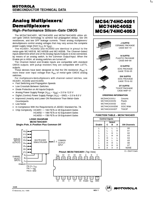
MC54/74HC4051 MC74HC4052 MC54/74HC4053
FUNCTION TABLE – MC74HC4052 LOGIC DIAGRAM MC74HC4052 Double–Pole, 4–Position Plus Common Off
X0 14 X1 15 X2 11 X3 Y0 Y1 Y2 Y3 A B
1 5 2 4 10 9 6 12
Control Inputs Select Enable L L L L H X = Don’t Care B L L H H X A L H L H X ON Channels Y0 Y1 Y2 Y3 NONE X0 X1 X2 X3
3
X
COMMON OUTPUT/ INPUT
Pinout: MC54/74HC4051 (Top View)
VCC 16 X2 15 X1 14 X0 13 X3 12 A 11 B 10
1 X4
10/95
2 X6
3 X
4 X7
5 X5
6
7
8 GND
Enable VEE
© Motorola, Inc. 1995
1 Y1
2 Y0
3 Z1
4 Z
5 Z0
6
7
Enable VEE
8 GND
MOTOROLA
2
High–Speed CMOS Logic Data DL129 — Rev 6
元器件交易网
ÎÎÎÎÎÎÎÎÎÎÎÎÎÎÎÎÎÎÎÎÎÎÎ Î Î Î ÎÎÎÎÎÎÎÎÎÎÎÎÎÎÎÎÎÎÎÎÎÎÎ Î Î Î ÎÎÎ Î Î Î ÎÎÎÎÎÎÎÎÎÎÎÎÎÎÎÎÎÎÎÎÎÎÎ Î Î Î ÎÎÎÎÎÎÎÎÎÎÎÎÎÎÎÎÎÎÎÎÎÎÎ Î Î Î ÎÎÎ Î Î Î ÎÎÎÎÎÎÎÎÎÎÎÎÎÎÎÎÎÎÎÎÎÎÎ Î Î Î ÎÎÎÎÎÎÎÎÎÎÎÎÎÎÎÎÎÎÎÎÎÎÎ ÎÎÎÎÎÎÎÎÎÎÎÎÎÎÎÎÎÎÎÎÎ Î Î ÎÎÎÎÎÎÎÎÎÎÎÎÎÎÎÎÎÎÎÎÎÎÎ Î Î Î ÎÎÎÎÎÎÎÎÎÎÎÎÎÎÎÎÎÎÎÎÎÎÎ Î Î Î ÎÎÎÎÎÎÎÎÎÎÎÎÎÎÎÎÎÎÎÎÎÎÎ Î Î Î ÎÎÎÎÎÎÎÎÎÎÎÎÎÎÎÎÎÎÎÎÎÎÎ Î Î Î ÎÎÎÎÎÎÎÎÎÎÎÎÎÎÎÎÎÎÎÎÎÎÎ Î Î Î ÎÎÎÎÎÎÎÎÎÎÎÎÎÎÎÎÎÎÎÎÎÎÎ Î Î Î ÎÎÎ Î Î Î ÎÎÎÎÎÎÎÎÎÎÎÎÎÎÎÎÎÎÎÎÎÎÎ Î Î Î ÎÎÎÎÎÎÎÎÎÎÎÎÎÎÎÎÎÎÎÎÎÎÎ Î Î Î ÎÎÎÎÎÎÎÎÎÎÎÎÎÎÎÎÎÎÎÎÎÎÎ Î Î Î ÎÎÎÎÎÎÎÎÎÎÎÎÎÎÎÎÎÎÎÎÎÎÎ Î Î Î ÎÎÎÎÎÎÎÎÎÎÎÎÎÎÎÎÎÎÎÎÎÎÎ Î Î Î ÎÎÎÎÎÎÎÎÎÎÎÎÎÎÎÎÎÎÎÎÎÎÎ ÎÎÎÎÎÎÎÎÎÎÎÎÎÎÎÎÎÎÎÎÎ Î Î ÎÎÎÎÎÎÎÎÎÎÎÎÎÎÎÎÎÎÎÎÎÎÎ Î Î Î ÎÎÎÎÎÎÎÎÎÎÎÎÎÎÎÎÎÎÎÎÎÎÎ Î Î Î ÎÎÎÎÎÎÎÎÎÎÎÎÎÎÎÎÎÎÎÎÎÎÎ Î Î Î ÎÎÎÎÎÎÎÎÎÎÎÎÎÎÎÎÎÎÎÎÎÎÎ Î Î Î ÎÎÎÎÎÎÎÎÎÎÎÎÎÎÎÎÎÎÎÎÎÎÎ Î Î Î ÎÎÎÎÎÎÎÎÎÎÎÎÎÎÎÎÎÎÎÎÎÎÎ Î Î Î ÎÎÎÎÎÎÎÎÎÎÎÎÎÎÎÎÎÎÎÎÎÎÎ Î Î Î ÎÎÎÎÎÎÎÎÎÎÎÎÎÎÎÎÎÎÎÎÎÎÎ Î Î Î ÎÎÎÎÎÎÎÎÎÎÎÎÎÎÎÎÎÎÎÎÎÎÎ Î Î Î ÎÎÎÎÎÎÎÎÎÎÎÎÎÎÎÎÎÎÎÎÎÎÎ Î Î Î ÎÎÎÎÎÎÎÎÎÎÎÎÎÎÎÎÎÎÎÎÎÎÎ Î Î Î ÎÎÎÎÎÎÎÎÎÎÎÎÎÎÎÎÎÎÎÎÎÎÎ Î Î Î ÎÎÎÎÎÎÎÎÎÎÎÎÎÎÎÎÎÎÎÎÎÎÎ Î Î Î ÎÎÎÎÎÎÎÎÎÎÎÎÎÎÎÎÎÎÎÎÎÎÎ Î Î Î ÎÎÎÎÎÎÎÎÎÎÎÎÎÎÎÎÎÎÎÎÎÎÎ Î Î Î ÎÎÎÎÎÎÎÎÎÎÎÎÎÎÎÎÎÎÎÎÎÎÎ Î ÎÎÎÎÎÎÎÎ Î Î Î ÎÎÎÎÎÎÎÎÎÎÎÎÎÎÎÎÎÎÎÎÎÎÎ ÎÎÎÎÎÎÎÎÎÎÎÎÎÎÎÎÎÎÎÎÎ ÎÎÎÎÎÎÎÎÎÎÎÎÎÎÎÎ Î ÎÎÎÎÎÎÎÎÎÎÎÎÎÎÎÎÎÎÎÎÎÎÎ ÎÎÎÎÎÎÎÎÎÎÎÎÎÎÎÎÎÎÎÎÎ Î Î ÎÎÎÎÎÎÎÎÎÎÎÎÎÎÎÎÎÎÎÎÎÎÎ ÎÎÎ ÎÎÎÎÎÎÎÎÎÎÎÎÎÎÎÎÎÎÎÎÎÎÎ Î Î ÎÎÎÎÎÎÎÎÎÎÎÎÎÎÎÎÎÎÎÎÎÎÎ
74HC02中文资料
74
Vcc=最大
VI=5.5V VI=7V
‘02 最小 最大
-1.5
2.4 2.4
0.4 0.4 1
‘S02 最小 最大
-1.2 2.5 2.7
0.5 0.5 1
‘LS02 最小 最大
-1.5 2.5 2.7
0.4 0.5
0.1
单位 V V V mA
IIH输入高电平电流
w Vcc=最大
VIH=2.4V VIH=2.7V
tPLH
12ns 3.6ns
tphl
8ns 3.5ns
PD
85mW 108mW
co
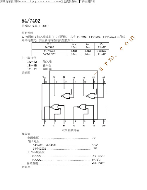
引出端符号 1A-4A
54/74LS02 输入端
10ns
10ns
11mW
.
m
1B-4B 1Y-4Y 逻辑图
输入端 输出端
-ar
a
g
p
f
.
w
ቤተ መጻሕፍቲ ባይዱ
w
w
双列直插封装 极限值
电源电压 …………………………………………. 7V 输入电压
4.75 5
5.25
2
0.8
c 54LS02/74LS02
最小 额定 最大
. 4.5
5
5.5
4.75 5 5.25
m 2
MC74HC00ADR2G,MC74HC00ADTR2G,MC74HC00ADG,MC74HC00ANG,规格书,Datasheet 资料
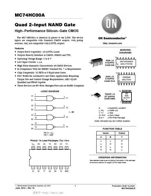
MC74HC00AQuad 2-Input NAND GateHigh −Performance Silicon −Gate CMOSThe MC74HC00A is identical in pinout to the LS00. The device inputs are compatible with Standard CMOS outputs; with pullup resistors, they are compatible with LSTTL outputs.Features•Output Drive Capability: 10 LSTTL Loads•Outputs Directly Interface to CMOS, NMOS and TTL •Operating V oltage Range: 2 to 6 V •Low Input Current: 1 m A•High Noise Immunity Characteristic of CMOS Devices•In Compliance With the JEDEC Standard No. 7 A Requirements •Chip Complexity: 32 FETs or 8 Equivalent Gates•NLV Prefix for Automotive and Other Applications Requiring Unique Site and Control Change Requirements; AEC −Q100Qualified and PPAP Capable•These Devices are Pb −Free, Halogen Free and are RoHS CompliantY1A1PIN 14 = V CC PIN 7 = GNDLOGIC DIAGRAMB1Y2A2B2Y3A3B3Y4A4B4Y = AB Pinout: 14−Lead Packages (Top View)1314121110982134567V CC B4A4Y4B3A3Y3A1B1Y1A2B2Y2GNDL L H HLH L HFUNCTION TABLEInputs Output AB H H H LY See detailed ordering and shipping information in the package dimensions section on page 2 of this data sheet.ORDERING INFORMATIONMARKING DIAGRAMSA = Assembly Location L, WL = Wafer Lot Y , YY = YearW, WW = Work WeekG or G = Pb −Free PackageTSSOP −14DT SUFFIX CASE 948GSOIC −14D SUFFIX CASE 751AHC 00A ALYW G G114PDIP −14N SUFFIX CASE 646MC74HC00AN AWLYYWWG114(Note: Microdot may be in either location)MAXIMUM RATINGSSymbol Parameter Value Unit V CC DC Supply Voltage (Referenced to GND)– 0.5 to + 7.0V V in DC Input Voltage (Referenced to GND)– 0.5 to V CC + 0.5V V out DC Output Voltage (Referenced to GND)– 0.5 to V CC + 0.5VI in DC Input Current, per Pin±20mA I out DC Output Current, per Pin±25mA I CC DC Supply Current, V CC and GND Pins ±50mAP DPower Dissipation in Still Air,Plastic DIP†SOIC Package†TSSOP Package†750500450mWT stg Storage Temperature – 65 to + 150_C T LLead Temperature, 1 mm from Case for 10 SecondsPlastic DIP , SOIC or TSSOP Package260_CStresses exceeding Maximum Ratings may damage the device. Maximum Ratings are stress ratings only. Functional operation above the Recommended Operating Conditions is not implied. Extended exposure to stresses above the Recommended Operating Conditions may affect device reliability.†Derating —Plastic DIP: – 10 mW/_C from 65_ to 125_CSOIC Package: – 7 mW/_C from 65_ to 125_C TSSOP Package: − 6.1 mW/_C from 65_ to 125_CRECOMMENDED OPERATING CONDITIONSSymbol Parameter Min Max Unit V CC DC Supply Voltage (Referenced to GND)2.0 6.0V V in , V out DC Input Voltage, Output Voltage (Referenced to GND)0V CCVT AOperating Temperature, All Package Types – 55+ 125_C t r , t fInput Rise and Fall TimeV CC = 2.0 V(Figure 1)V CC = 4.5 V V CC = 6.0 V001000500400nsORDERING INFORMATIONDevicePackage Shipping †MC74HC00ANG PDIP −14(Pb −Free)25 Units / Rail MC74HC00ADG SOIC −14(Pb −Free)55 Units / Rail MC74HC00ADR2G SOIC −14(Pb −Free)2500 / Tape & Reel MC74HC00ADTR2G TSSOP −14(Pb −Free)2500 / Tape & Reel NLV74HC00ADG*SOIC −14(Pb −Free)55 Units / Rail NLV74HC00ADR2G*SOIC −14(Pb −Free)2500 / Tape & Reel NLV74HC00ADTR2G*TSSOP −14(Pb −Free)2500 / Tape & Reel NLV74HC00ANG*PDIP −14(Pb −Free)25 Units / Rail†For information on tape and reel specifications, including part orientation and tape sizes, please refer to our Tape and Reel Packaging Specifications Brochure, BRD8011/D.*NLV Prefix for Automotive and Other Applications Requiring Unique Site and Control Change Requirements; AEC −Q100 Qualified and PPAP CapableThis device contains protection circuitry to guard against damage due to high static voltages or electric fields. However, precautions must be taken to avoid applications of any voltage higher than maximum rated voltages to this high −impedance cir-cuit. For proper operation, V in and V out should be constrained to the range GND v (V in or V out ) v V CC .Unused inputs must always be tied to an appropriate logic voltage level (e.g., either GND or V CC ).Unused outputs must be left open.DC CHARACTERISTICS(Voltages Referenced to GND)V CC V Guaranteed LimitSymbol Parameter Condition−55 to 25°C≤85°C≤125°C UnitV IH Minimum High−Level InputVoltage V out = 0.1V or V CC−0.1V|I out| ≤ 20m A2.03.04.56.01.502.103.154.201.502.103.154.201.502.103.154.20VV IL Maximum Low−Level InputVoltage V out = 0.1V or V CC− 0.1V|I out| ≤ 20m A2.03.04.56.00.500.901.351.800.500.901.351.800.500.901.351.80VV OH Minimum High−Level OutputVoltage V in = V IH or V IL|I out| ≤ 20m A2.04.56.01.94.45.91.94.45.91.94.45.9VV in =V IH or V IL|I out| ≤ 2.4mA|I out| ≤ 4.0mA|I out| ≤ 5.2mA3.04.56.02.483.985.482.343.845.342.203.705.20V OL Maximum Low−Level OutputVoltage V in = V IH or V IL|I out| ≤ 20m A2.04.56.00.10.10.10.10.10.10.10.10.1VV in = V IH or V IL|I out| ≤ 2.4mA|I out| ≤ 4.0mA|I out| ≤ 5.2mA3.04.56.00.260.260.260.330.330.330.400.400.40I in Maximum Input LeakageCurrentV in = V CC or GND 6.0±0.1±1.0±1.0m AI CC Maximum Quiescent SupplyCurrent (per Package)V in = V CC or GNDI out = 0m A6.0 1.01040m AAC CHARACTERISTICS(C L = 50 pF, Input t r = t f = 6 ns)V CC V Guaranteed LimitSymbol Parameter−55 to 25°C≤85°C≤125°C Unitt PLH, t PHL Maximum Propagation Delay, Input A or B to Output Y(Figures 1 and 2)2.03.04.56.07530151395401916110552219nst TLH, t THL Maximum Output Transition Time, Any Output(Figures 1 and 2)2.03.04.56.07527151395321916110362219nsC in Maximum Input Capacitance101010pFC PD Power Dissipation Capacitance (Per Buffer)*Typical @ 25°C, V CC = 5.0 V, V EE = 0 VpF22*Used to determine the no−load dynamic power consumption: P D = C PD V CC f + I CC V CC.Figure 1. Switching WaveformsGNDV CCOUTPUT YINPUT A OR BC L **Includes all probe and jig capacitanceTESTPOINTFigure 2. Test CircuitYA BFigure 3. Expanded Logic Diagram(1/4 of the Device)PDIP−14 N SUFFIX CASE 646−06 ISSUE PDIM MIN MAX MIN MAXMILLIMETERSINCHESA0.7150.77018.1619.56B0.2400.260 6.10 6.60C0.1450.185 3.69 4.69D0.0150.0210.380.53F0.0400.070 1.02 1.78G0.100 BSC 2.54 BSCH0.0520.095 1.32 2.41J0.0080.0150.200.38K0.1150.135 2.92 3.43LM−−−10 −−−10N0.0150.0390.38 1.01__NOTES:1.DIMENSIONING AND TOLERANCING PER ANSIY14.5M, 1982.2.CONTROLLING DIMENSION: INCH.3.DIMENSION L TO CENTER OF LEADS WHENFORMED PARALLEL.4.DIMENSION B DOES NOT INCLUDE MOLD FLASH.5.ROUNDED CORNERS OPTIONAL.KM0.13 (0.005)0.2900.3107.377.87CASE 751A −03ISSUE KNOTES:1.DIMENSIONING AND TOLERANCING PER ASME Y14.5M, 1994.2.CONTROLLING DIMENSION: MILLIMETERS.3.DIMENSION b DOES NOT INCLUDE DAMBAR PROTRUSION. ALLOWABLE PROTRUSION SHALL BE 0.13 TOTAL IN EXCESS OF AT MAXIMUM MATERIAL CONDITION.4.DIMENSIONS D AND E DO NOT INCLUDE MOLD PROTRUSIONS.5.MAXIMUM MOLD PROTRUSION 0.15 PERSIDE.DETAIL ADIM MIN MAX MIN MAX INCHESMILLIMETERS D 8.558.750.3370.344E 3.80 4.000.1500.157A 1.35 1.750.0540.068b 0.350.490.0140.019L 0.40 1.250.0160.049e 1.27 BSC 0.050 BSC A30.190.250.0080.010A10.100.250.0040.010M0 7 0 7 H 5.80 6.200.2280.244h 0.250.500.0100.019____14X0.581.27PITCH*For additional information on our Pb −Free strategy and soldering details, please download the ON Semiconductor Soldering and Mounting Techniques Reference Manual, SOLDERRM/D.DT SUFFIX CASE 948G −01ISSUE BDIM MIN MAX MIN MAX INCHESMILLIMETERS A 4.90 5.100.1930.200B 4.30 4.500.1690.177C −−− 1.20−−−0.047D 0.050.150.0020.006F 0.500.750.0200.030G 0.65 BSC 0.026 BSC H 0.500.600.0200.024J 0.090.200.0040.008J10.090.160.0040.006K 0.190.300.0070.012K10.190.250.0070.010L 6.40 BSC 0.252 BSC M0 8 0 8 NOTES:1.DIMENSIONING AND TOLERANCING PER ANSI Y14.5M, 1982.2.CONTROLLING DIMENSION: MILLIMETER.3.DIMENSION A DOES NOT INCLUDE MOLD FLASH, PROTRUSIONS OR GATE BURRS.MOLD FLASH OR GATE BURRS SHALL NOT EXCEED 0.15 (0.006) PER SIDE.4.DIMENSION B DOES NOT INCLUDE INTERLEAD FLASH OR PROTRUSION.INTERLEAD FLASH OR PROTRUSION SHALL NOT EXCEED 0.25 (0.010) PER SIDE.5.DIMENSION K DOES NOT INCLUDE DAMBAR PROTRUSION. ALLOWABLE DAMBAR PROTRUSION SHALL BE 0.08(0.003) TOTAL IN EXCESS OF THE K DIMENSION AT MAXIMUM MATERIAL CONDITION.6.TERMINAL NUMBERS ARE SHOWN FOR REFERENCE ONLY .7.DIMENSION A AND B ARE TO BE DETERMINED AT DATUM PLANE −W −.____14X REF 14X0.360.65PITCHSOLDERING FOOTPRINT**For additional information on our Pb −Free strategy and soldering details, please download the ON Semiconductor Soldering and Mounting Techniques Reference Manual, SOLDERRM/D.ON Semiconductor and are registered trademarks of Semiconductor Components Industries, LLC (SCILLC). SCILLC reserves the right to make changes without further notice to any products herein. SCILLC makes no warranty, representation or guarantee regarding the suitability of its products for any particular purpose, nor does SCILLC assume any liability arising out of the application or use of any product or circuit, and specifically disclaims any and all liability, including without limitation special, consequential or incidental damages.“Typical” parameters which may be provided in SCILLC data sheets and/or specifications can and do vary in different applications and actual performance may vary over time. All operating parameters, including “Typicals” must be validated for each customer application by customer’s technical experts. SCILLC does not convey any license under its patent rights nor the rights of others. SCILLC products are not designed, intended, or authorized for use as components in systems intended for surgical implant into the body, or other applications intended to support or sustain life, or for any other application in which the failure of the SCILLC product could create a situation where personal injury or death may occur. Should Buyer purchase or use SCILLC products for any such unintended or unauthorized application, Buyer shall indemnify and hold SCILLC and its officers, employees, subsidiaries, affiliates, and distributors harmless against all claims, costs, damages, and expenses, and reasonable attorney fees arising out of, directly or indirectly, any claim of personal injury or death associated with such unintended or unauthorized use, even if such claim alleges that SCILLC was negligent regarding the design or manufacture of the part. SCILLC is an Equal Opportunity/Affirmative Action Employer. This literature is subject to all applicable copyright laws and is not for resale in any manner.PUBLICATION ORDERING INFORMATION。
TC74VHC4052AFT中文资料
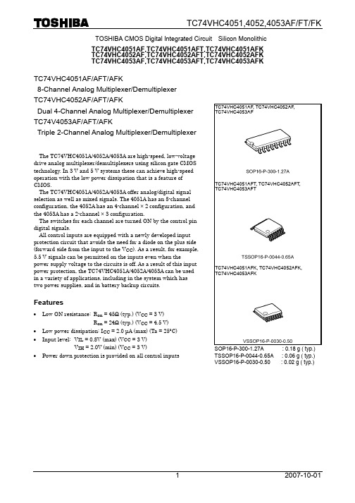
Truth Table
Control Inputs
Inhibit
C*
B
A
L
L
L
L
L
L
L
H
L
L
H
L
L
L
H
H
L
H
L
L
L
H
L
H
L
H
H
L
L
H
H
H
Hห้องสมุดไป่ตู้
X
X
X
X: Don't care, *: Except VHC4052AFT
VHC4051A 0 1 2 3 4 5 6 7
None
“ON” Channel VHC4052A 0X, 0Y 1X, 1Y 2X, 2Y 3X, 3Y ⎯ ⎯ ⎯ ⎯ None
元器件交易网
TC74VHC4051,4052,4053AF/FT/FK
TOSHIBA CMOS Digital Integrated Circuit Silicon Monolithic TC74VHC4051AF,TC74VHC4051AFT,TC74VHC4051AFK TC74VHC4052AF,TC74VHC4052AFT,TC74VHC4052AFK TC74VHC4053AF,TC74VHC4053AFT,TC74VHC4053AFK
Operating Range (Note)
Characteristics
Symbol
Rating
Unit
Power supply voltage Input voltage Switch I/O voltage Operating temperature
74HC4052电路使用说明手册中文版
时 Vis=VEE, RL 到 VDD,如图 3 所示
3. RL=10KΩ;CL=50pF 到 VEE ; E = VDD (方波);测量 tPHZ 和 tPZH 时,Vis=VDD,RL 到 VEE ;测量 tPLZ
VDD(V) 功率计算公式(μW)
一块电路的动态 功率耗散(P)
5
1300fi+∑(f0CL)×VDD2
9
6100fi+∑(f0CL)×VDD2
fi 是输入频率(MHz) f0 是输出频率(MHz) CL 是负载电容(pF) ∑(f0CL)是输出之和 VDD 是电源电压(V)
参数
VDD(V) 符号
典型 最大 单 位
பைடு நூலகம்
无锡中微爱芯电子有限公司
Wuxi I-CORE Electronics Co., Ltd.
编号:74HC4052-AX-BJ-47
i-core 图2 导通电阻是输入电压的函数(Iis=200μΑVSS=VEE=0V)
3.3.2、交流特性(VSS=VEE=0V;Tamb=25℃;输入跃变时间≤20ns)
第 9 页 共 15 页 版本:2012-01-B1
表 733-11-I
4、应用说明
电路工作区域
无锡中微爱芯电子有限公司
Wuxi I-CORE Electronics Co., Ltd.
编号:74HC4052-AX-BJ-47
i-core
江苏省无锡市蠡园经济开发区滴翠路 100 号 9 栋 2 层
备注
74HC4052
FUNCTION TABLE INPUT(1) CHANNEL BETWEEN E L L L L H Note 1. H = HIGH voltage level L = LOW voltage level X = don’t care. S1 L L H H X S0 L H L H X nY0 and nZ nY1 and nZ nY2 and nZ nY3 and nZ none
74HC4052; 74HCT4052
TYPICAL SYMBOL tPZH/tPZL tPHZ/tPLZ CI CPD CS PARAMETER turn-on time E or Sn to Vos turn-off time E or Sn to Vos input capacitance power dissipation capacitance per switch notes 1 and 2 maximum switch capacitance independent (Y) common (Z) Notes 1. CPD is used to determine the dynamic power dissipation (PD in µW). PD = CPD × VCC2 × fi × N + Σ[(CL + CS) × VCC2 × fo] where: fi = input frequency in MHz; fo = output frequency in MHz; CL = output load capacitance in pF; CS = maximum switch capacitance in pF; VCC = supply voltage in Volts; N = number of inputs switching; Σ[(CL + CS) × VCC2 × fo] = sum of the outputs. 2. For 74HC4052 the condition is VI = GND to VCC For 74HCT4052 the condition is VI = GND to VCC − 1.5 V. ORDERING INFORMATION PACKAGE TYPE NUMBER 74HC4052D 74HCT4052D 74HC4052DB 74HCT4052DB 74HC4052N 74HCT4052N 74HC4052PW 74HC4052BQ 74HCT4052BQ TEMPERATURE RANGE −40 °C to +125 °C −40 °C to +125 °C −40 °C to +125 °C −40 °C to +125 °C −40 °C to +125 °C −40 °C to +125 °C −40 °C to +125 °C −40 °C to +125 °C −40 °C to +125 °C PINS 16 16 16 16 16 16 16 16 16 PACKAGE SO16 SO16 SSOP16 SSOP16 DIP16 DIP16 TSSOP16 DHVQFN16 DHVQFN16 MATERIAL plastic plastic plastic plastic plastic plastic plastic plastic plastic CODE SOT109-3 SOT109-3 SOT338-1 SOT338-1 SOT38-9 SOT38-9 SOT403-1 SOT763-1 SOT763-1 CONDITIONS 74HC4052 74HCT4052 CL = 15 pF; RL = 1 kΩ; VCC = 5 V CL = 15 pF; RL = 1 kΩ; VCC = 5 V 28 21 3.5 57 5 12 18 13 3.5 57 5 12 ns ns pF pF pF pF UNIT
高性能硅制栅极COMSMC74HC4051AMC74HC4052A和MC74HC
高性能硅制栅极COMS
MC74HC4051A, MC74HC4052A和MC74HC4053A利用硅制栅极COMS技术来得到快速传播延迟,低导通阻抗和低断开漏电流。
这些模拟多路复用器、信号分离器控制在电压范围内所有模拟电压。
HC4051A, HC4052A and和HC4053A和金属栅极的MC14051AB, MC14052AB and MC14053AB.引脚相同。
通过输入通道的选择决定模拟输入中的哪个输入、输出,用模拟开关与普通的输入输出相连。
当Enable引脚是高电平时,所有模拟开关断开。
通道选择和Enable输入是与coms的输出相协调的;通过上拉电阻器他们可以与LSTTL的输出相协调。
设计这种驱动的目的就是让ON电阻在输入电压的作用下工作的线性程度比用用金属栅极COMS模拟开关更好。
HC4851A and HC4852A是具有输入电流保护的多路复用器、信号分离器。
特点
开关和传输速度快
开关之间相互干扰小
所有输入、输出引脚都有二极管保护
模拟电压输入范围(V CC − V EE) = 2.0 to 12.0 V
数字(控制)电压输入范围(V CC − GND) = 2.0 to 6.0 V
在线性度和低ON阻抗方面的性能较金属栅极的好
低噪音
符合JEDEC标准第七A
芯片的复杂度:HC4051A — 184 FETs or 46 Equivalent Gates
HC4052A — 168 FETs or 42 Equivalent Gates
HC4053A — 156 FETs or 39 Equivalent Gates
无铅包装。
CD4052

74HC/HCT4052双重4通道模拟多路复用器/多路信号分离器特性◆宽模拟输入电压范围:±5V ◆低通电阻抗:当Vcc- V EE = 4.5V 时为80Ω(标准值) 当Vcc- V EE = 6.0V 时为70Ω (标准值) 当Vcc- V EE = 9.0V 时为60Ω (标准值) ◆逻辑电平变换:可以实现5V 逻辑电平与±5V 模拟信号之间的通讯 ◆内置特有的“break before make ”电路(先拆后合)◆输出能力:非标准◆Icc 分类:MSI (中规模集成电路)总述74HC/HCT4052是高速硅门COMS 元件,其引脚与“4000B ”系列的“4052”兼容。
此IC 符合JEDEC 标准no.7A 。
74HC/HCT4052双重四通道模拟多路复用器/多路信号分离器,带有公共选择逻辑。
每个多路复用器有四个独立的输入/输出(nY0 ~ nY3)和一个公共输入/输出端(nZ )。
公共通道选择逻辑包括了两个数字选择输入(S0及S1)和一个低电平有效的输入端(E )。
当E 为低,通过S0与S1可以选择四个开关中的一个(低阻抗的“开-状态”)。
当E 为高时,所有开关都处于高阻抗的“关-状态”,不受S0与S1控制。
Vcc 与GND 是数字控制输入端(S0与S1,E )的供电引脚。
Vcc 与GND 的范围是:HC 系列为2.0至10.0V ;HCT 系列为4.5至5.5V 。
模拟输入端/输出端(nY0至nY3,nZ )的电压可以在Vcc (正极限)与V EE (负极限)之间摆动。
Vcc-V EE 不可以超过10.0V 。
当作为数字多路复用器/多路信号分离器使用时,V EE 要连接到GND (标准地)。
快速参考数据EE f 注释1、 C PD 用于决定动态功率损耗(P D 单位为uW )2、对于HC ,Vi = GND 对Vcc 电压(){}OCC L i CC PD D f V C C f V C P ⨯⨯+∑+⨯⨯=252: 对于HCL ,Vi = GND 对Vcc – 1.5V=i f 输入频率,单位:MHz =O f 输出频率,单位:MHz(){}=⨯⨯+∑OCC S L f V C C 2输出端总和L C = 输出负载电容,单位:pFS C = 最大开关电容,单位:pFVcc = 供电电压,单位:V引脚描述引脚号符号名称与功能1,5,2,4 2Y0至2Y3 独立输入端/输出端6 E 输入使能(低电平有效)7 VEE 负供电电压8 GND 地(0V)10,9 S0,S1 选择输入端12,14,15,11 1Y0至1Y3 独立输入端/输出端13,3 1Z,2Z 公共输入端/输出端16 Vcc 正供电电压额定值各电压均以VEE=GND(ground=0V)为参考点符号参数最小值最大值单位条件Vcc 直流供电电压- 0.5 +11.0 V±I IK直流数字输入二极管电流20 mA Vi< -0.5V或Vi> Vcc+0.5V ±I SK直流开关二极管电流20 mA Vs< -0.5V或Vs>Vcc+0.5V ±I S直流开关电流25 mA - 0.5V<Vs<Vcc+0.5V±I EE直流VEE电流20 mA±Icc; ±I GND直流Vcc或GND电流50 mATstg 存储温度范围-65 +150 ℃Ptot 芯片总功率损耗:塑封DIL(双列直插式)塑封迷你封装(SO)750500mWmW温度范围:- 40至+125℃大于+70℃:以12mW/K的比例线性下降大于+70℃:以8mW/k的比例线性下降Ps 各开关功率损耗100 mW建议工作条件符号参数74HC 74HCT单位条件最小标准最大最小标准最大Vcc 直流供电电压Vcc-GND2.0 5.0 10.0 4.5 5.0 5.5Vcc 直流供电电压Vcc-VEE2.0 5.0 10.0 2.0 5.0 10.0Vi 直流输入电压范围GND Vcc GND VccVs 直流开关电压范围V EE Vcc V EE VccTamb 工作环境温度范围-40 +85 -40 +85Tamb 工作环境温度范围-40 +125 -40 +125t r, t f输入端上升和降时间6.0 10005004002506.0 50074HC/HCT直流特性74HC: Vcc-GND 或Vcc-VEE=2.0, 4.5, 6.0及9.0V74HC直流特性以下均为对地(GND=0)电压值。
74系列功能大全(中文)

74系列功能大全(中文)74、74HC、74LS系列芯片资料,从网上下的,集合了一下系列电平典型传输延迟ns 最大驱动电流(-Ioh/Lol)mAAHC CMOS 8.5 -8/8AHCT COMS/TTL 8.5 -8/8HC COMS 25 -8/8HCT COMS/TTL 25 -8/8ACT COMS/TTL 10 -24/24F TTL 6.5 -15/64ALS TTL 10 -15/64LS TTL 18 -15/24注:同型号的74系列、74HC系列、74LS系列芯片,逻辑功能上是一样的。
74LSxx的使用说明如果找不到的话,可参阅74xx或74HCxx的使用说明。
有些资料里包含了几种芯片,如74HC161资料里包含了74HC160、74HC161、74HC162、74HC163四种芯片的资料。
找不到某种芯片的资料时,可试着查看一下临近型号的芯片资料。
7400 QUAD 2-INPUT NAND GATES 与非门7401 QUAD 2-INPUT NAND GATES OC 与非门7402 QUAD 2-INPUT NOR GATES 或非门7403 QUAD 2-INPUT NAND GATES 与非门7404 HEX INVERTING GATES 反向器7406 HEX INVERTING GATES HV 高输出反向器7408 QUAD 2-INPUT AND GATE 与门7409 QUAD 2-INPUT AND GATES OC 与门7410 TRIPLE 3-INPUT NAND GATES 与非门7411 TRIPLE 3-INPUT AND GATES 与门74121 ONE-SHOT WITH CLEAR 单稳态74132 SCHMITT TRIGGER NAND GATES 触发器与非门7414 SCHMITT TRIGGER INVERTERS 触发器反向器74153 4-LINE TO 1 LINE SELECTOR 四选一74155 2-LINE TO 4-LINE DECODER 译码器74180 PARITY GENERATOR/CHECKER 奇偶发生检验74191 4-BIT BINARY COUNTER UP/DOWN 计数器7420 DUAL 4-INPUT NAND GATES 双四输入与非门7426 QUAD 2-INPUT NAND GATES 与非门7427 TRIPLE 3-INPUT NOR GATES 三输入或非门7430 8-INPUT NAND GATES 八输入端与非门7432 QUAD 2-INPUT OR GATES 二输入或门7438 2-INPUT NAND GATE BUFFER 与非门缓冲器7445 BCD-DECIMAL DECODER/DRIVER BCD译码驱动器7474 D-TYPE FLIP-FLOP D型触发器7475 QUAD LATCHES 双锁存器7476 J-K FLIP-FLOP J-K触发器7485 4-BIT MAGNITUDE COMPARATOR 四位比较器7486 2-INPUT EXCLUSIVE OR GATES 双端异或门74HC00 QUAD 2-INPUT NAND GATES 双输入与非门74HC02 QUAD 2-INPUT NOR GATES 双输入或非门74HC03 2-INPUT OPEN-DRAIN NAND GATES 与非门74HC04 HEX INVERTERS 六路反向器74HC05 HEX INVERTERS OPEN DRAIN 六路反向器74HC08 2-INPUT AND GATES 双输入与门74HC107 J-K FLIP-FLOP WITH CLEAR J-K触发器74HC109A J-K FLIP-FLOP W/PRESET J-K触发器74HC11 TRIPLE 3-INPUT AND GATES 三输入与门74HC112 DUAL J-K FLIP-FLOP 双J-K触发器74HC113 DUAL J-K FLIP-FLOP PRESET 双JK触发器74HC123A RETRIGGERABLE MONOSTAB 可重触发单稳74HC125 TRI-STATE QUAD BUFFERS 四个三态门74HC126 TRI-STATE QUAD BUFFERS 六三态门74HC132 2-INPUT TRIGGER NAND 施密特触发与非门74HC133 13-INPUT NAND GATES 十三输入与非门74HC137 3-TO-8 DECODERS W/LATCHES 3-8线译码器74HC138 3-8 LINE DECODER 3线至8线译码器74HC139 2-4 LINE DECODER 2线至4线译码器74HC14 TRIGGERED HEX INVERTER 六触发反向器74HC147 10-4 LINE PRIORITY ENCODER 10-4编码器74HC148 8-3 LINE PRIORITY ENCODER 8-3编码器74HC149 8-8 LINE PRIORITY ENCODER 8-8编码器74HC151 8-CHANNEL DIGITAL MUX 8通道多路器74HC153 DUAL 4-INPUT MUX 双四输入多路器74HC154 4-16 LINE DECODER 4线至16线译码器74HC155 2-4 LINE DECODER 2线至4线译码器74HC157 QUAD 2-INPUT MUX 四个双端多路器74HC161 BINARY COUNTER 二进制计数器74HC163 DECADE COUNTERS 十进制计数器74HC164 SERIAL-PARALLEL SHIFT REG 串入并出74HC165 PARALLEL-SERIAL SHIFT REG 并入串出74HC166 SERIAL-PARALLEL SHIFT REG 串入并出74HC173 TRI-STATE D FLIP-FLOP 三态D触发器74HC174 HEX D FLIP-FLOP W/CLEAR 六D触发器74HC175 HEX D FLIP-FLOP W/CLEAR 六D触发器74HC181 ARITHMETIC LOGIC UNIT 算术逻辑单元74HC182 LOOK AHEAD CARRYGENERATR 进位发生器74HC190 BINARY UP/DN COUNTER 二进制加减计数器74HC191 DECADE UP/DN COUNTER 十进制加减计数器74HC192 DECADE UP/DN COUNTER 十进制加减计数器74HC193 BINARY UP/DN COUNTER 二进制加减计数器74HC194 4BIT BI-DIR SHIFT 4位双向移位寄存器74HC195 4BIT PARALLEL SHIFT 4位并行移位寄存器74HC20 QUAD 4-INPUT NAND GATE 四个四入与非门74HC221A NON-RETRIG MONOSTAB 不可重触发单稳74HC237 3-8 LINE DECODER 地址锁3线至8线译码器74HC242/243 TRI-STAT TRANSCEIVER 三态收发器74HC244 OCTAL 3-STATE BUFFER 八个三态缓冲门74HC245 OCTAL 3-STATE TRANSCEIVER 三态收发器74HC251 8-CH 3-STATE MUX 8路3态多路器74HC253 DUAL 4-CH 3-STATE MUX 4路3态多路器74HC257 QUAD 2-CH 3-STATE MUX 4路3态多路器74HC258 2-CH 3-STATE MUX 2路3态多路器74HC259 3-8 LINE DECODER 8位地址锁存译码器74HC266A 2-INPUT EXCLUSIVE NOR GATE 异或非74HC27 TRIPLE 3-INPUT NOR GATE三个3输入或非门74HC273 OCTAL D FLIP-FLOP CLEAR 8路D触发器74HC280 9BIT ODD/EVEN GENERATOR 奇偶发生器74HC283 4BIT BINARY ADDER CARRY 四位加法器74HC299 3-STATE UNIVERSAL SHIFT 三态移位寄存74HC30 8-INPUT NAND GATE 8输入端与非门74HC32 QUAD 2-INPUT OR GATE 四个双端或门74HC34 NON-INVERTER 非反向器74HC354 8-CH 3-STATE MUX 8路3态多路器74HC356 8-CH 3-STATE MUX 8路3态多路器74HC365 HEX 3-STATE BUFFER 六个三态缓冲门74HC366 3-STATE BUFFER INVERTER 缓冲反向器74HC367 3-STATE BUFFER INVERTER 缓冲反向器74HC368 3-STATE BUFFER INVERTER 缓冲反向器74HC373 3-STATE OCTAL D LATCHES 三态D型锁存器74HC374 3-STATE OCTAL D FLIPFLOP 三态D触发器74HC393 4-BIT BINARY COUNTER 4位二进制计数器74HC4016 QUAD ANALOG SWITCH 四路模拟量开关74HC4020 14-Stage Binary Counter 14输出计数器74HC4017 Decade Counter/Divider with 10 Decoded Outputs 十进制计数器带10个译码输出端74HC4040 12 Stage Binary Counter 12出计数器74HC4046 PHASE LOCK LOOP 相位监测输出器74HC4049 LEVEL DOWN CONVERTER 电平变低器74HC4050 LEVEL DOWN CONVERTER 电平变低器74HC4051 8-CH ANALOG MUX 8通道多路器74HC4052 4-CH ANALOG MUX 4通道多路器74HC4053 2-CH ANALOG MUX 2通道多路器74HC4060 14-STAGE BINARY COUNTER 14阶BIN计数74HC4066 QUAD ANALOG MUX 四通道多路器74HC4075 TRIPLE 3-INPUT OR GATE 3输入或门74HC42 BCD TO DECIMAL BCD转十进制译码器74HC423A RETRIGGERABLE MONOSTAB 可重触发单稳74HC4511 BCD-7 SEG DRIVER/DECODER 7段译码器74HC4514 4-16 LINE DECODER 4至16线译码器74HC4538A RETRIGGERAB MONOSTAB 可重触发单稳74HC4543 LCD BCD-7 SEG LCD用的BCD-7段译码驱动74HC51 AND OR GATE INVERTER 与或非门74HC521 8BIT MAGNITUDE COMPARATOR 判决定路74HC533 3-STATE D LATCH 三态D锁存器74HC534 3-STATE D FLIP-FLOP 三态D型触发器74HC540 3-STATE BUFFER 三态缓冲器74HC541 3-STATE BUFFER INVERTER三态缓冲反向器74HC58 DUAL AND OR GATE 与或门74HC589 3STATE 8BIT SHIFT 8位移位寄存三态输出74HC594 8BIT SHIFT REG 8位移位寄存器74HC595 8BIT SHIFT REG 8位移位寄存器出锁存74HC597 8BIT SHIFT REG 8位移位寄存器入锁存74HC620 3-STATE TRANSCEIVER 反向3态收发器74HC623 3-STATE TRANSCEIVER 八路三态收发器74HC640 3-STATE TRANSCEIVER 反向3态收发器74HC643 3-STATE TRANSCEIVER 八路三态收发器74HC646 NON-INVERT BUS TRANSCEIVER 总线收发器74HC648 INVERT BUS TRANCIVER 反向总线收发器74HC688 8BIT MAGNITUDE COMPARATOR 8位判决电路74HC7266 2-INPUT EXCLUSIVE NOR GATE 异或非门74HC73 DUAL J-K FLIP-FLOP W/CLEAR 双JK触发器74HC74A PRESET/CLEAR D FLIP-FLOP 双D触发器74HC75 4BIT BISTABLE LATCH 4位双稳锁存器74HC76 PRESET/CLEAR JK FLIP-FLOP 双JK触发器74HC85 4BIT MAGNITUDE COMPARATOR 4位判决电路74HC86 2INPUT EXCLUSIVE OR GATE 2输入异或门74HC942 BAUD MODEM 300BPS低速调制解调器74HC943 300 BAUD MODEM 300BPS低速调制解调器74LS00 QUAD 2-INPUT NAND GATES 与非门74LS02 QUAD 2-INPUT NOR GATES 或非门74LS03 QUAD 2-INPUT NAND GATES 与非门74LS04 HEX INVERTING GATES 反向器74LS05 HEX INVERTERS OPEN DRAIN 六路反向器74LS08 QUAD 2-INPUT AND GATE 与门74LS09 QUAD 2-INPUT AND GATES OC 与门74LS10 TRIPLE 3-INPUT NAND GATES 与非门74LS109 QUAD 2-INPUT AND GATES OC 与门74LS11 TRIPLE 3-INPUT AND GATES 与门74LS112 DUAL J-K FLIP-FLOP 双J-K触发器74LS113 DUAL J-K FLIP-FLOP PRESET 双JK触发器74LS114 NEGATIVE J-K FLIP-FLOP 负沿J-K触发器74LS122 Retriggerable Monostab 可重触发单稳74LS123 Retriggerable Monostable 可重触发单稳74LS125 TRI-STATE QUAD BUFFERS 四个三态门74LS13 QUAL 4-in NAND TRIGGER 4输入与非触发器74LS160 BCD DECADE 4BIT BIN COUNTERS 计数器74LS136 QUADRUPLE 2-INPUT XOR GATE 异或门74LS138 3-8 LINE DECODER 3线至8线译码器74LS139 2-4 LINE DECODER 2线至4线译码器74LS14 TRIGGERED HEX INVERTER 六触发反向器74HC147 10-4 LINE PRIORITY ENCODER 10-4编码器74HC148 8-3 LINE PRIORITY ENCODER 8-3编码器74HC149 8-8 LINE PRIORITY ENCODER 8-8编码器74LS151 8-CHANNEL DIGITAL MUX 8通道多路器74LS153 DUAL 4-INPUT MUX 双四输入多路器74LS155 2-4 LINE DECODER 2线至4线译码器74LS156 2-4 LINE DECODER/DEMUX 2-4译码器74LS157 QUAD 2-INPUT MUX 四个双端多路器74LS158 2-1 LINE MUX 2-1线多路器74LS160A BINARY COUNTER 二进制计数器74LS161A BINARY COUNTER 二进制计数器74LS162A BINARY COUNTER 二进制计数器74LS163A DECADE COUNTERS 十进制计数器74LS164 SERIAL-PARALLEL SHIFT REG 串入并出74LS168 BI-DIRECT BCD TO DECADE 双向计数器74LS169 4BIT UP/DN BIN COUNTER 四位加减计数器74LS173 TRI-STATE D FLIP-FLOP 三态D触发器74LS174 HEX D FLIP-FLOP W/CLEAR 六D触发器74LS175 HEX D FLIP-FLOP W/CLEAR 六D触发器74LS190 BINARY UP/DN COUNTER 二进制加减计数器74LS191 DECADE UP/DN COUNTER 十进制加减计数器74LS192 DECADE UP/DN COUNTER 十进制加减计数器74LS193 BINARY UP/DN COUNTER 二进制加减计数器74LS194A 4BIT BI-DIR SHIFT 4位双向移位寄存器74LS195A 4BIT PARALLEL SHIFT4位并行移位寄存器74LS20 QUAD 4-INPUT NAND GATE 四个四入与非门74LS21 4-INPUT AND GATE 四输入端与门74LS240 OCTAL 3-STATE BUFFER 八个三态缓冲门74LS244 OCTAL 3-STATE BUFFER 八个三态缓冲门74LS245 OCTAL 3-STATE TRANSCEIVER 三态收发器74LS253 DUAL 4-CH 3-STATE MUX 4路3态多路器74LS256 4BIT ADDRESS LATCH 四位可锁存锁存器74LS257 QUAD 2-CH 3-STATE MUX 4路3态多路器74LS258 2-CH 3-STATE MUX 2路3态多路器74LS27 TRIPLE 3-INPUT NOR GATES 三输入或非门74LS279 QUAD R-S LATCHES 四个RS非锁存器74LS28 QUAD 2-INPUT NOR BUFFER 四双端或非缓冲74LS283 4BIT BINARY ADDER CARRY 四位加法器74LS30 8-INPUT NAND GATES 八输入端与非门74LS32 QUAD 2-INPUT OR GATES 二输入或门74LS352 4-1 LINE SELECTOR/MUX 4-1线选择多路器74LS365 HEX 3-STATE BUFFER 六个三态缓冲门74LS367 3-STATE BUFFER INVERTER 缓冲反向器74LS368A 3-STATE BUFFER INVERTER 缓冲反向器74LS373 OCT LATCH W/3-STATE OUT三态输出锁存器74LS76 Dual JK Flip-Flop w/set 2个JK触发器74LS379 QUAD PARALLEL REG 四个并行寄存器74LS38 2-INPUT NAND GATE BUFFER 与非门缓冲器74LS390 DUAL DECADE COUNTER 2个10进制计数器74LS393 DUAL BINARY COUNTER 2个2进制计数器74LS42 BCD TO DECIMAL BCD转十进制译码器74LS48 BCD-7 SEG BCD-7段译码器74LS49 BCD-7 SEG BCD-7段译码器74LS51 AND OR GATE INVERTER 与或非门74LS540 OCT Buffer/Line Driver 8路缓冲驱动器74LS541 OCT Buffer/LineDriver 8路缓冲驱动器74LS74 D-TYPE FLIP-FLOP D型触发器74LS682 8BIT MAGNITUDE COMPARATOR 8路比较器74LS684 8BIT MAGNITUDE COMPARATOR 8路比较器74LS75 QUAD LATCHES 双锁存器74LS83A 4BIT BINARY ADDER CARRY 四位加法器74LS85 4BIT MAGNITUDE COMPARAT 4位判决电路74LS86 2INPUT EXCLUSIVE OR GATE 2输入异或门74LS90 DECADE/BINARY COUNTER 十/二进制计数器74LS95B 4BIT RIGHT/LEFT SHIFT 4位左右移位寄存74LS688 8BIT MAGNITUDE COMPARAT 8位判决电路74LS136 2-INPUT XOR GATE 2输入异或门74LS651 BUS TRANSCEIVERS 总线收发器74LS653 BUS TRANSCEIVERS 总线收发器74LS670 3-STATE 4-BY-4 REG 3态4-4寄存器74LS73A DUAL J-K FLIP-FLOP W/CLEAR 双JK触发器。
cd4052芯片手册
cd4052芯片手册一、产品概述CD4052是一款由模拟公司(Analog Devices)生产的双路2输入多路复用器/解复用器芯片。
它具有16个通道,通过两个单片控制输入端进行选择,可以将两个独立的模拟输入信号中的一个传输到输出端。
二、产品特点1.高速:CD4052的传输速率高达50MHz,适合用于高速数据传输和信号处理。
2.高精度:CD4052的模拟信号传输精度高,能够保证信号的完整性和准确性。
3.灵活:CD4052可以通过控制输入端选择不同的通道,实现多种不同的信号传输和分配方案。
4.易于使用:CD4052的接口简单,只需要两个单片控制输入端即可实现信号的选择和传输。
三、应用领域CD4052广泛应用于通信、雷达、电子对抗、仪器仪表、自动测试设备等领域,用于实现高速、高精度、灵活的信号传输和处理。
四、工作原理CD4052由两个独立的输入缓冲器和一个多路复用器组成。
当控制输入端为低电平时,多路复用器选择第一个缓冲器的输出;当控制输入端为高电平时,多路复用器选择第二个缓冲器的输出。
通过改变控制输入端的电平,可以实现不同通道之间的切换。
五、使用方法在使用CD4052时,需要根据具体的应用场景和需求进行选择和控制。
需要根据输入信号的特性和要求选择合适的缓冲器和多路复用器,并根据需要配置控制输入端的电平以选择不同的通道。
同时,需要注意接口的匹配和抗干扰问题,以保证信号的稳定传输。
六、常见问题及解决方法在使用CD4052过程中,可能会遇到一些常见问题,如信号失真、噪声干扰等。
可以通过优化电路设计、加强信号调理和滤波等措施解决这些问题。
同时,需要注意芯片的功耗和散热问题,以保证其正常工作。
七、典型应用电路在使用CD4052时,可以参考其典型应用电路进行设计和配置。
典型应用电路可以根据具体的应用场景和需求进行选择和调整。
需要注意的是,在实际应用中需要根据电路的具体情况进行适当的调整和优化,以保证信号的稳定传输和处理的准确性。
M74HC4052B1R资料

V
VCC - VEE Supply Voltage Range
-0.5 to 13
V
VIN
Control Input Voltage
-0.5 to VCC + 0.5
V
VI/O
Switch I/O Voltage
ICK
Control Input Diode Current
IIOK
I/O Diode Current
Difference of ON Resistance Between Switches
Test Conditions
VCC VEE (V) (V)
TA = 25 oC 54HC and 74HC
Value
-40 to 85 oC -55 to 125 oC Unit
74HC
54HC
Min. Typ. Max. Min. Max. Min. Max.
VEE - 0.5 to VCC + 0.5
V
± 20
mA
± 20
mA
IT
Switch Through Current
± 25
mA
ICC
DC VCC or Ground Current
± 50
mA
PD
Power Dissipation
Tstg
Storage Temperature
TL
Lead Temperature (10 sec)
5/15
元器件交易网
M54/M74HC4051/4052/4053
RECOMMENDED OPERATING CONDITIONS
Symbol VCC VEE
VCC - VEE VIN VI/O Top
MM74HC4052

August 1984Revised May 1999MM74HC4051 • MM74HC4052 • MM74HC4053 8-Channel Analog Multiplexer •© 1999 Fairchild Semiconductor Corporation DS005353.prf MM74HC4051 • MM74HC4052 • MM74HC40538-Channel Analog Multiplexer •Dual 4-Channel Analog Multiplexer •Triple 2-Channel Analog MultiplexerGeneral DescriptionThe MM74HC4051, MM74HC4052 and MM74HC4053multiplexers are digitally controlled analog switches imple-mented in advanced silicon-gate CMOS technology. These switches have low “on” resistance and low “off” leakages.They are bidirectional switches, thus any analog input may be used as an output and vice-versa. Also these switches contain linearization circuitry which lowers the on resis-tance and increases switch linearity. These devices allow control of up to ±6V (peak) analog signals with digital con-trol signals of 0 to 6V. Three supply pins are provided for V CC , ground, and V EE . This enables the connection of 0–5V logic signals when V CC = 5V and an analog input range of ±5V when V EE = 5V. All three devices also have an inhibit control which when HIGH will disable all switches to their off state. All analog inputs and outputs and digital inputs are protected from electrostatic damage by diodes to V CC and ground.MM74HC4051: This device connects together the outputs of 8 switches, thus achieving an 8 channel Multiplexer. The binary code placed on the A, B, and C select lines deter-mines which one of the eight switches is “on”, and con-nects one of the eight inputs to the common output.MM74HC4052: This device connects together the outputs of 4 switches in two sets, thus achieving a pair of 4-channel multiplexers. The binary code placed on the A, and B select lines determine which switch in each 4 channel sec-tion is “on”, connecting one of the four inputs in each sec-tion to its common output. This enables the implementation of a 4-channel differential multiplexer.MM74HC4053: This device contains 6 switches whose out-puts are connected together in pairs, thus implementing a triple 2 channel multiplexer, or the equivalent of 3 single-pole-double throw configurations. Each of the A, B, or C select lines independently controls one pair of switches,selecting one of the two switches to be “on”.Featuress Wide analog input voltage range: ±6V s Low “on” resistance:50 typ. (V CC –V EE = 4.5V)30 typ. (V CC –V EE = 9V)s Logic level translation to enable 5V logic with ±5V ana-log signals s Low quiescent current: 80 µA maximum (74HC)s Matched Switch characteristicOrdering Code:Devices also available in T ape and Reel. Specify by appending the suffix letter “X” to the ordering code.Order Number Package NumberPackage DescriptionMM74HC4051M M16A 16-Lead Small Outline Integrated Circuit (SOIC), JEDEC MS-012, 0.150” Narrow MM74HC4051WM M16B 16-Lead Small Outline Integrated Circuit (SOIC), JEDEC MS-013, 0.300” Wide MM74HC4051SJ M16D 16-Lead Small Outline Package (SOP), EIAJ TYPE II, 5.3mm WideMM74HC4051MTC MTC1616-Lead Thin Shrink Small Outline Package (TSSOP), JEDEC MO-153, 4.4mm Wide MM74HC4051N N16E 16-Lead Plastic Dual-In-Line Package (PDIP), JEDEC MS-0010.300” Wide MM74HC4052M M16A 16-Lead Small Outline Integrated Circuit (SOIC), JEDEC MS-012, 0.150” Narrow MM74HC4052WM M16B 16-Lead Small Outline Integrated Circuit (SOIC), JEDEC MS-013, 0.300” Wide MM74HC4052SJ M16D 16-Lead Small Outline Package (SOP), EIAJ TYPE II, 5.3mm WideMM74HC4052MTC MTC1616-Lead Thin Shrink Small Outline Package (TSSOP), JEDEC MO-153, 4.4mm Wide MM74HC4052N N16E 16-Lead Plastic Dual-In-Line Package (PDIP), JEDEC MS-0010.300” Wide MM74HC4053M M16A 16-Lead Small Outline Integrated Circuit (SOIC), JEDEC MS-012, 0.150” Narrow MM74HC4053WM M16B 16-Lead Small Outline Integrated Circuit (SOIC), JEDEC MS-013, 0.300” Wide MM74HC4053SJ M16D 16-Lead Small Outline Package (SOP), EIAJ TYPE II, 5.3mm WideMM74HC4053MTC MTC1616-Lead Thin Shrink Small Outline Package (TSSOP), JEDEC MO-153, 4.4mm Wide MM74HC4053NN16E16-Lead Plastic Dual-In-Line Package (PDIP), JEDEC MS-0010.300” Wide 2M M 74H C 4051 • M M 74H C 4052 • M M 74H C 4053Connection DiagramsPin Assignments for DIP , SOIC, SOP and TSSOPTop ViewTop ViewTop ViewTruth TablesMM744051MM744052MM744053Input“ON”Inh C B A Channel H X X X None L L L L Y0L L L H Y1L L H L Y2L L H H Y3L H L L Y4L H L H Y5L H H L Y6LHHHY7Inputs “ON” Channels Inh B A X Y H X X None None L L L 0X 0Y L L H 1X 1Y L H L 2X 2Y LHH3X3YInput“ON” Channels Inh C B A C b a H X X X None None NoneL L LLCX BX AX L LL HCX BX AY L L H L CX BY AX L L H H CX BY AY L H LLCY BX AX L H L H CY BX AY L H H L CY BY AX LH H HCYBYAYMM74HC4051 • MM74HC4052 • MM74HC4053Logic DiagramsMM74HC4051MM74HC4052MM74HC4053 4M M 74H C 4051 • M M 74H C 4052 • M M 74H C 4053Absolute Maximum Ratings (Note 1)(Note 2)Recommended Operating ConditionsNote 1: Absolute Maximum Ratings are those values beyond which dam-age to the device may occur.Note 2: Unless otherwise specified all voltages are referenced to ground.Note 3: Power Dissipation temperature derating — plastic “N” package: −12 mW/°C from 65°C to 85°C.DC Electrical Characteristics (Note 4)Supply Voltage (V CC )−0.5 to +7.5V Supply Voltage (V EE )+0.5 to −7.5V Control Input Voltage (V IN )−1.5 to V CC +1.5V Switch I/O Voltage (V IO )V EE −0.5 to V CC +0.5VClamp Diode Current (I IK , I OK )±20 mA Output Current, per pin (I OUT )±25 mA V CC or GND Current, per pin (I CC )±50 mAStorage Temperature Range (T STG )−65°C to +150°CPower Dissipation (P D )(Note 3)600 mW S.O. Package only 500 mW Lead Temperature (T L )(Soldering 10 seconds)260°C MinMax Units Supply Voltage (V CC )26V Supply Voltage (V EE )0−6VDC Input or Output Voltage (V IN , V OUT )0V CC V Operating Temperature Range (T A )−40+85°CInput Rise or Fall Times (t r , t f ) V CC = 2.0V1000ns V CC = 4.5V 500ns V CC = 6.0V400nsSymbol ParameterConditionsV EEV CC T A = 25°C T A = −40 to 85°C T A = −55 to 125°CUnits TypGuaranteed Limits V IHMinimum HIGH Level 2.0V 1.5 1.5 1.5V Input Voltage4.5V 3.15 3.15 3.15V 6.0V 4.2 4.2 4.2V V ILMaximum LOW Level 2.0V 0.50.50.5V Input Voltage4.5V 1.35 1.35 1.35V 6.0V1.8 1.8 1.8V R ONMaximum “ON” Resistance V INH = V IL , I S = 2.0 mA GND 4.5V 40160200240Ω(Note 5)V IS = V CC to V EE −4.5V 4.5V 30120150170Ω(Figure 1)−6.0V 6.0V 20100125140ΩV INH = V IL , I S = 2.0 mA GND 2.0V 100230280320ΩV IS = V CC or V EE GND 4.5V 40110140170Ω(Figure 1)−4.5V 4.5V 2090120140Ω−6.0V 6.0V 1580100115ΩR ONMaximum “ON” Resistance V CTL = V ILGND 4.5V 10202525ΩMatchingV IS = V CC to GND −4.5V 4.5V 5101515Ω−6.0V 6.0V5101215ΩI IN Maximum Control V IN = V CC or GND ±0.1±1.0±1.0µAInput Current V CC = 2−6V I CC Maximum Quiescent V IN = V CC or GND GND 6.0V 880160µA Supply Current I OUT = 0 µA −6.0V 6.0V 16160320µA I IZMaximum Switch “OFF”V OS = V CC or V EE GND 6.0V ±60±600±600nA Leakage Current V IS = V EE or V CC −6.0V 6.0V±100±1000±1000nA(Switch Input)V INH = V IH (Figure 2)I IZMaximum Switch V IS = V CC to V EEGND 6.0V ±0.2±2.0±2.0µA “ON” Leakage HC4051V INH = V IL−6.0V 6.0V±0.4±4.0±4.0µACurrent(Figure 3)V IS = V CC to V EEGND 6.0V ±0.1±1.0±1.0µA HC4052V INH = V IL (Figure 3)−6.0V 6.0V ±0.2±2.0±2.0µA V IS = V CC to V EEGND 6.0V ±0.1±1.0±1.0µA HC4053V INH = V IL (Figure 3)−6.0V 6.0V±0.1±1.0±1.0µAMM74HC4051 • MM74HC4052 • MM74HC4053DC Electrical Characteristics (Continued)Note 4: For a power supply of 5V ±10% the worst case on resistances (R ON ) occurs for HC at 4.5V. Thus the 4.5V values should be used when designing with this supply. Worst case V IH and V IL occur at V CC = 5.5V and 4.5V respectively. (The V IH value at 5.5V is 3.85V.) The worst case leakage current occur for CMOS at the higher voltage and so the 5.5V values should be used.Note 5: At supply voltages (V CC –V EE ) approaching 2V the analog switch on resistance becomes extremely non-linear. Therefore it is recommended that these devices be used to transmit digital only when using these supply voltages.AC Electrical CharacteristicsV CC = 2.0V −6.0V, V EE = 0V −6V, C L = 50 pF (unless otherwise specified)Symbol ParameterConditions V EE V CCT A = 25°C T A = −40 to 85°C T A = −55 to 125°CUnits TypGuaranteed Limits I IZMaximum Switch V OS = V CC or V EEGND 6.0V ±0.2±2.0±2.0µA “OFF” Leakage HC4051V IS = V EE or V CC−6.0V 6.0V ±0.4±4.0±4.0µA Current (Common Pin)V INH = V IHV OS = V CC or V EEGND 6.0V ±0.1±1.0±1.0µA HC4052V IS = V EE or V CC−6.0V 6.0V ±0.2±2.0±2.0µA V INH = V IHV OS = V CC or V EEGND 6.0V ±0.1±1.0±1.0µA HC4053V IS = V EE or V CC−6.0V 6.0V±0.1±1.0±1.0µAV INH = V IHSymbolParameterConditionsV EE V CC T A = 25°C T A = −40 to 85°C T A = −55 to 125°CUnits Typ Guaranteed Limitst PHL , t PLH Maximum PropagationGND 2.0V 25607590ns Delay Switch In to OutGND 4.5V 5121518ns −4.5V 4.5V 481214ns −6.0V6.0V 371113ns t PZL , t PZH Maximum Switch TurnR L = 1 k ΩGND 2.0V 92355435515ns “ON” DelayGND 4.5V 6987103ns −4.5V 4.5V 16465869ns −6.0V6.0V 15415162ns t PHZ , t PLZ Maximum Switch TurnGND 2.0V 65290365435ns “OFF” DelayGND 4.5V 28587387ns −4.5V 4.5V 18374656ns −6.0V6.0V 16324148ns f MAXMinimum Switch GND 4.5V 30MHz Frequency Response −4.5V4.5V35MHz20 log (V I /V O ) = 3 dB Control to Switch R L = 600Ω,V IS = 4 V PP 0V 4.5V 1080mV Feedthrough Noise f = 1 MHz,V IS = 8 V PP−4.5V4.5V250mVC L = 50 pF Crosstalk between R L = 600Ω,V IS = 4 V PP 0V 4.5−52dB any Two Switches f = 1 MHz V IS = 8 V PP −4.5V 4.5V −50dB Switch OFF Signal R L = 600Ω,V IS = 4 V PP 0V 4.5V −42dB Feedthrough f = 1 MHz,V IS = 8 V PP−4.5V4.5V−44dBIsolationV CTL = V IL THDSinewave Harmonic R L = 10 k Ω,V IS = 4 V PP 0V 4.5V 0.013%DistortionC L = 50 pF,V IS = 8 V PP−4.5V4.5V0.008%f = 1 kHzC IN Maximum Control 5101010pFInput Capacitance C INMaximum Switch Input15pFInput Capacitance4051 Common 904052 Common 454053 Common30C INMaximum Feedthrough Capacitance5pF 6M M 74H C 4051 • M M 74H C 4052 • M M 74H C 4053AC Test Circuits and Switching Time WaveformsFIGURE 1. “ON” ResistanceFIGURE 2. “OFF” Channel Leakage CurrentFIGURE 3. “ON” Channel Leakage CurrentFIGURE 4. t PHL, t PLH Propagation Delay Time Signal Input to Signal OutputFIGURE 5. t PZL, t PLZ Propagation Delay Time Control to Signal OutputFIGURE 6. t PZH, t PHZ Propagation Delay Time Control to Signal OutputMM74HC4051 • MM74HC4052 • MM74HC4053AC Test Circuits and Switching Time Waveforms (Continued)FIGURE 7. Crosstalk: Control Input to Signal OutputFIGURE 8. Crosstalk Between Any Two SwitchesTypical Performance CharacteristicsTypical “On” Resistance vs Input VoltageV CC =−V EESpecial ConsiderationsIn certain applications the external load-resistor current may include both V CC and signal line components. Toavoid drawing V CC current when switch current flows into the analog switch pins, the voltage drop across the switch must not exceed 1.2V (calculated from the ON resistance). 8M M 74H C 4051 • M M 74H C 4052 • M M 74H C 4053Physical Dimensionsinches (millimeters) unless otherwise noted16-Lead Small Outline Integrated Circuit (SOIC), JEDEC MS-012, 0.150” NarrowPackage Number M16A16-Lead Small Outline Integrated Circuit (SOIC), JEDEC MS-013, 0.300” WidePackage Number M16B MM74HC4051 • MM74HC4052 • MM74HC4053Physical Dimensions inches (millimeters) unless otherwise noted (Continued)16-Lead Small Outline Package (SOP), EIAJ TYPE II, 5.3mm WidePackage Number M16D 10M M 74H C 4051 • M M 74H C 4052 • M M 74H C 4053Physical Dimensionsinches (millimeters) unless otherwise noted (Continued)16-Lead Thin Shrink Small Outline Package (TSSOP), JEDEC MO-153, 4.4mm WidePackage Number MTC16Fairchild does not assume any responsibility for use of any circuitry described, no circuit patent licenses are implied and Fairchild reserves the right at any time without notice to change said circuitry and specifications.MM74HC4051• MM74HC4052 • MM74HC4053 8-Channel Analog Multiplexer •LIFE SUPPORT POLICYFAIRCHILD’S PRODUCTS ARE NOT AUTHORIZED FOR USE AS CRITICAL COMPONENTS IN LIFE SUPPORT DEVICES OR SYSTEMS WITHOUT THE EXPRESS WRITTEN APPROVAL OF THE PRESIDENT OF FAIRCHILD SEMICONDUCTOR CORPORATION. As used herein:1.Life support devices or systems are devices or systemswhich, (a) are intended for surgical implant into thebody, or (b) support or sustain life, and (c) whose failureto perform when properly used in accordance withinstructions for use provided in the labeling, can be rea-sonably expected to result in a significant injury to the user.2. A critical component in any component of a life support device or system whose failure to perform can be rea-sonably expected to cause the failure of the life support device or system, or to affect its safety or Physical Dimensions inches (millimeters) unless otherwise noted (Continued)16-Lead Plastic Dual-In-Line Package (PDIP), JEDEC MS-001, 0.300” WidePackage Number N16E。
CD74HCT4052技术资料

TG S0 11
TG
S1 10 S2 9
LOGIC LEVEL CONVERSION
BINARY TO
1 OF 8 DECODER
WITH ENABLE
TG A
3 COMMON OUT/IN
TG
TG
TG E6
TG
8
7
GND
VEE
ENABLE L L L L L L L L H
X = Don’t care
CAUTION: These devices are sensitive to electrostatic discharge. Users should follow proper IC Handling Procedures.
Copyright © 2004, Texas Instruments Incorporated
Data sheet acquired from Harris Semiconductor SCHS122I
November 1997 - Revised July 2004
CD54/74HC4051, CD54/74HCT4051, CD54/74HC4052, CD74HCT4052, CD54/74HC4053, CD74HCT4053
CD74HC4053PWT
-55 to 125 16 Ld TSSOP
CD74HCT4051E
-55 to 125 16 Ld PDIP
CD74HCT4051M
-55 to 125 16 Ld SOIC
CD74HCT4051MT
-55 to 125 16 Ld SOIC
CD74HCT4051M96
-55 to 125 16 Ld SOIC
74LV4052中文资料
元器件交易网DIP16:plastic dual in-line package; 16 leads (300 mil)SOT38-4SO16:plastic small outline package; 16 leads; body width 3.9 mm SOT109-1SSOP16:plastic shrink small outline package; 16 leads; body width 5.3 mm SOT338-1TSSOP16:plastic thin shrink small outline package; 16 leads; body width 4.4 mm SOT403-1Philips Semiconductors and Philips Electronics North America Corporation reserve the right to make changes, without notice, in the products,including circuits, standard cells, and/or software, described or contained herein in order to improve design and/or performance. Philips Semiconductors assumes no responsibility or liability for the use of any of these products, conveys no license or title under any patent, copyright,or mask work right to these products, and makes no representations or warranties that these products are free from patent, copyright, or mask work right infringement, unless otherwise specified. Applications that are described herein for any of these products are for illustrative purposes only. Philips Semiconductors makes no representation or warranty that such applications will be suitable for the specified use without further testing or modification.LIFE SUPPORT APPLICATIONSPhilips Semiconductors and Philips Electronics North America Corporation Products are not designed for use in life support appliances, devices,or systems where malfunction of a Philips Semiconductors and Philips Electronics North America Corporation Product can reasonably be expected to result in a personal injury. Philips Semiconductors and Philips Electronics North America Corporation customers using or selling Philips Semiconductors and Philips Electronics North America Corporation Products for use in such applications do so at their own risk and agree to fully indemnify Philips Semiconductors and Philips Electronics North America Corporation for any damages resulting from such improper use or sale.This data sheet contains preliminary data, and supplementary data will be published at a later date. Philips Semiconductors reserves the right to make changes at any time without notice in order to improve design and supply the best possible product.Philips Semiconductors 811 East Arques Avenue P .O. Box 3409Sunnyvale, California 94088–3409Telephone 800-234-7381DEFINITIONSData Sheet IdentificationProduct StatusDefinitionObjective SpecificationPreliminary Specification Product Specification Formative or in DesignPreproduction ProductFull ProductionThis data sheet contains the design target or goal specifications for product development. Specifications may change in any manner without notice.This data sheet contains Final Specifications. Philips Semiconductors reserves the right to make changes at any time without notice, in order to improve design and supply the best possible product.© Copyright Philips Electronics North America Corporation 1998All rights reserved. Printed in U.S.A.print codeDate of release: 05-96。
74HC_HCT4052
3 of 27
NXP Semiconductors
74HC4052; 74HCT4052
Dual 4-channel analog multiplexer/demultiplexer
6. Pinning information
6.1 Pinning
74HC4052 74HCT4052
2Y0 2Y2 2Z 2Y3 2Y1 E VEE GND 1 2 3 4 5 6 7 8
Fig 5.
Pin configuration for DIP16, SO16 and (T)SSOP16
Fig 6.
Pin configuration for DHVQFN16
6.2 Pin description
Table 2. Symbol 2Y0 2Y2 2Z 2Y3 2Y1 E VEE GND S1 S0 1Y3 1Y0 1Z 1Y1 1Y2 VCC Pin description Pin 1 2 3 4 5 6 7 8 9 10 11 12 13 14 15 16 Description independent input or output 2Y0 independent input or output 2Y2 common input or output 2 independent input or output 2Y3 independent input or output 2Y1 enable input (active LOW) negative supply voltage ground (0 V) select logic input 1 select logic input 0 independent input or output 1Y3 independent input or output 1Y0 common input or output 1 independent input or output 1Y1 independent input or output 1Y2 positive supply voltage
HD74HC4053中文资料

— 70 140 — 175
VI/O ≤ 2 mA
— 50 — — —
Ω
VINH = VIL
— 13 40 — 50
VI/O = VCC to VEE
— 10 20 — 25
II/O ≤ 2 mA
—
—
±0.1 —
±1.0 µA VINH = VIL
OFF channel
IS (ON)
6.0
—
—
±0.1 —
Ta = 25°C
Ta = –40 to +85°C
Item
Symbol VCC (V) Min Typ
Control input voltage VIH
2.0
1.5 —
4.5
3.15 —
Max Min Max — 1.5 — — 3.15 —
Unit Test Conditions V
6.0
4.2 — — 4.2 —
Recommended Operating Range
Item
Symbol
Min
Typ
Max
Unit
Supply voltage
Control input voltage Switch I/O voltage Operating temperature
VCC – VEE
2
—
GND – VEE –4
—
Control input diode current
Switch I/O diode current
Power dissipation
Storage temperature range
Symbol VCC VCC – VEE VIN VI/O I CC I GND I I/O I IK I IOK PT Tstg
MC74LVXC3245DWR2中文资料
MC74LVXC3245Configurable Dual Supply Octal Transceiverwith 3−State Outputs for 3 V SystemsThe 74LVXC3245 is a 24−pin dual−supply, octal configurable voltage interface transceiver especially well suited for PCMCIA and other real time configurable I/O applications. The V CCA pin accepts a 3.0 V supply level; the A port is a dedicated 3.0 V port. The V CCB pin accepts a 3.0 V−to−5.0 V supply level. The B port is configured to track the V CCB supply level. A 5.0 V level on the V CCB pin will configure the I/O pins at a 5.0 V level and a 3.0 V V CCB will configure the I/O pins at a 3.0 V level. The A port interfaces with a 3.0 V host system and the B port to the card slots. This device will allow the V CCB voltage source pin and I/O pins on the B port to float when OE is High. This feature is necessary to buffer data to and from a PCMCIA socket that permits PCMCIA cards to be inserted and removed during normal operation. The Transmit/Receive (T/R) input determines the direction of data flow. Transmit (active−High) enables data from the A port to B port. Receive (active−Low) enables data from the B port to the A port.Features•Bidirectional Interface Between 3.0 V and 3.0 V/5.0 V Buses •Control Inputs Compatible with TTL Level •Outputs Source/Sink Up to 24 mA•Guaranteed Simultaneous Switching Noise Level and Dynamic Threshold Performance•Available in SOIC and TSSOP Packages •Flexible V CCB Operating Range•Allows B Port and V CCB to Float Simultaneously When OE is High •Functionally Compatible With the 74 Series 245•Pb−Free Packages are Available**For additional information on our Pb−Free strategy and soldering details, please download the ON Semiconductor Soldering and Mounting TechniquesReference Manual, SOLDERRM/D.MARKING DIAGRAMSSOIC−24See detailed ordering and shipping information in the package dimensions section on page 5 of this data sheet.ORDERING INFORMATION124LVXC3245AWLYYWW A =Assembly Location WL =Wafer Lot YY =YearWW =Work WeekLVX 3245AWLYYWW124TSSOP−24DT SUFFIX CASE 948HB0B1B2B3B4B5B6B7Figure 2. Logic Diagramand Transitions are Acceptable; for I CC reasons, Do Not Float InputsMAXIMUM RATINGSvalues (not normal operating conditions) and are not valid simultaneously. If these limits are exceeded, device functional operation is not implied, damage may occur and reliability may be affected.RECOMMENDED OPERATING CONDITIONSDC ELECTRICAL CHARACTERISTICS2.Max number of outputs defined as (n). Data inputs are driven 0 V to V CC level; one output at GND.3.Max number of data inputs (n) switching. (n−1) inputs switching 0 V to V CC level. Input under test switching: V CC level to threshold (V IHD),0 V to threshold (V ILD), f = 1 MHz.AC ELECTRICAL CHARACTERISTICSCCA CCB5.Typical values at V CCA = 3.3 V, V CCB = 3.3 V at 25°C.6.Skew is defined as the absolute value of the difference between the actual propagation delay for any two separate outputs of the same device.The specification applies to any outputs switching in the same direction, either HIGH−to−LOW (t OSHL) or LOW−to−HIGH (t OSLH); parameter guaranteed by design.CAPACITIVE CHARACTERISTICSORDERING INFORMATIONSpecifications Brochure, BRD8011/D.*This package is inherently Pb−Free.Figure 3. Block DiagramOPTIONALConfigurable I/O Application for PCMCIA CardsThe 74LVXC3245 is a dual−supply device well suited for PCMCIA configurable I/O applications. The LVXC3245consumes less than 1mW of quiescent power in all modes of operation, making it ideal for low power notebook designs.The L VXC3245 meets all PCMCIA I/O voltage requirements at 5.0 V and 3.3 V operation. By tying the V CCB pin to the card voltage supply, the PCMCIA card will always haverail−to−rail output swings, maximizing the reliability of the interface.The V CCA pin must always be tied to a 3.3 V power supply.This voltage connection provides internal references needed to account for variations in V CCB . When connected as in the figure above, the L VXC3245 meets all the voltage and current requirements of the ISA bus standard (IEEE P996).WAVEFORM 1 − PROPAGATION DELAYS t R = t F = 2.5 ns, 10% to 90%; f = 1 MHz; t W = 500 nsV CC0 VV OHV OLAn, BnBn, AnWAVEFORM 2 − OUTPUT ENABLE AND DISABLE TIMES t R = t F = 2.5 ns, 10% to 90%; f = 1 MHz; t W = 500 nsV CC0 V ≈ 0 VOE, T/RAn, Bn≈ V CC An, BnFigure 4. AC WaveformsV CCV OH − 0.3 V V OL + 0.3 V GNDOPEN2xV CC C L = 50 pF or equivalent (Includes jig and probe capacitance)R L = R 1 = 500 W or equivalentR T = Z OUT of pulse generator (typically 50 W )Figure 5. Test CircuitPACKAGE DIMENSIONSSOIC−24DW SUFFIX CASE 751E−04ISSUE ENOTES:1.DIMENSIONING AND TOLERANCING PER ANSI Y14.5M, 1982.2.CONTROLLING DIMENSION: MILLIMETER.3.DIMENSIONS A AND B DO NOT INCLUDE MOLD PROTRUSION.4.MAXIMUM MOLD PROTRUSION 0.15 (0.006)PER SIDE.5.DIMENSION D DOES NOT INCLUDE DAMBAR PROTRUSION. ALLOWABLE DAMBARPROTRUSION SHALL BE 0.13 (0.005) TOTAL IN EXCESS OF D DIMENSION AT MAXIMUM MATERIAL CONDITION.DIM MIN MAX MIN MAX INCHESMILLIMETERS A 15.2515.540.6010.612B 7.407.600.2920.299C 2.35 2.650.0930.104D 0.350.490.0140.019F 0.410.900.0160.035G 1.27 BSC 0.050 BSC J 0.230.320.0090.013K 0.130.290.0050.011M 0 8 0 8 P 10.0510.550.3950.415R0.250.750.0100.029____PACKAGE DIMENSIONSTSSOP−24DT SUFFIX CASE 948H−01ISSUE ANOTES:24X REFON Semiconductor and are registered trademarks of Semiconductor Components Industries, LLC (SCILLC). SCILLC reserves the right to make changes without further notice to any products herein. SCILLC makes no warranty, representation or guarantee regarding the suitability of its products for any particular purpose, nor does SCILLC assume any liability arising out of the application or use of any product or circuit, and specifically disclaims any and all liability, including without limitation special, consequential or incidental damages.“Typical” parameters which may be provided in SCILLC data sheets and/or specifications can and do vary in different applications and actual performance may vary over time. All operating parameters, including “Typicals” must be validated for each customer application by customer’s technical experts. SCILLC does not convey any license under its patent rights nor the rights of others. SCILLC products are not designed, intended, or authorized for use as components in systems intended for surgical implant into the body, or other applications intended to support or sustain life, or for any other application in which the failure of the SCILLC product could create a situation where personal injury or death may occur. Should Buyer purchase or use SCILLC products for any such unintended or unauthorized application, Buyer shall indemnify and hold SCILLC and its officers, employees, subsidiaries, affiliates, and distributors harmless against all claims, costs, damages, and expenses, and reasonable attorney fees arising out of, directly or indirectly, any claim of personal injury or death associated with such unintended or unauthorized use, even if such claim alleges that SCILLC was negligent regarding the design or manufacture of the part. SCILLC is an Equal Opportunity/Affirmative Action Employer. This literature is subject to all applicable copyright laws and is not for resale in any manner.PUBLICATION ORDERING INFORMATION。
MC74HC4052中文资料

X SWITCH
13
X COMMON OUTPUTS/INPUTS
ANALOG INPUTS/OUTPUTS
Y SWITCH
3
Y
Pinout: MC74HC4052 (Top View)
PIN 16 = VCC PIN 7 = VEE PIN 8 = GND VCC 16 X2 15 X1 14 X 13 X0 12 X3 11 A 10 B 9
1 Y1
2 Y0
3 Z1
4 Z
5 Z0
6
7
Enable VEE
8 GND
MOTOROLA
2
High–Speed CMOS Logic Data DL129 — Rev 6
元器件交易网
ÎÎÎÎÎÎÎÎÎÎÎÎÎÎÎÎÎÎÎÎÎÎÎ Î Î Î ÎÎÎÎÎÎÎÎÎÎÎÎÎÎÎÎÎÎÎÎÎÎÎ Î Î Î ÎÎÎ Î Î Î ÎÎÎÎÎÎÎÎÎÎÎÎÎÎÎÎÎÎÎÎÎÎÎ Î Î Î ÎÎÎÎÎÎÎÎÎÎÎÎÎÎÎÎÎÎÎÎÎÎÎ Î Î Î ÎÎÎ Î Î Î ÎÎÎÎÎÎÎÎÎÎÎÎÎÎÎÎÎÎÎÎÎÎÎ Î Î Î ÎÎÎÎÎÎÎÎÎÎÎÎÎÎÎÎÎÎÎÎÎÎÎ ÎÎÎÎÎÎÎÎÎÎÎÎÎÎÎÎÎÎÎÎÎ Î Î ÎÎÎÎÎÎÎÎÎÎÎÎÎÎÎÎÎÎÎÎÎÎÎ Î Î Î ÎÎÎÎÎÎÎÎÎÎÎÎÎÎÎÎÎÎÎÎÎÎÎ Î Î Î ÎÎÎÎÎÎÎÎÎÎÎÎÎÎÎÎÎÎÎÎÎÎÎ Î Î Î ÎÎÎÎÎÎÎÎÎÎÎÎÎÎÎÎÎÎÎÎÎÎÎ Î Î Î ÎÎÎÎÎÎÎÎÎÎÎÎÎÎÎÎÎÎÎÎÎÎÎ Î Î Î ÎÎÎÎÎÎÎÎÎÎÎÎÎÎÎÎÎÎÎÎÎÎÎ Î Î Î ÎÎÎ Î Î Î ÎÎÎÎÎÎÎÎÎÎÎÎÎÎÎÎÎÎÎÎÎÎÎ Î Î Î ÎÎÎÎÎÎÎÎÎÎÎÎÎÎÎÎÎÎÎÎÎÎÎ Î Î Î ÎÎÎÎÎÎÎÎÎÎÎÎÎÎÎÎÎÎÎÎÎÎÎ Î Î Î ÎÎÎÎÎÎÎÎÎÎÎÎÎÎÎÎÎÎÎÎÎÎÎ Î Î Î ÎÎÎÎÎÎÎÎÎÎÎÎÎÎÎÎÎÎÎÎÎÎÎ Î Î Î ÎÎÎÎÎÎÎÎÎÎÎÎÎÎÎÎÎÎÎÎÎÎÎ ÎÎÎÎÎÎÎÎÎÎÎÎÎÎÎÎÎÎÎÎÎ Î Î ÎÎÎÎÎÎÎÎÎÎÎÎÎÎÎÎÎÎÎÎÎÎÎ Î Î Î ÎÎÎÎÎÎÎÎÎÎÎÎÎÎÎÎÎÎÎÎÎÎÎ Î Î Î ÎÎÎÎÎÎÎÎÎÎÎÎÎÎÎÎÎÎÎÎÎÎÎ Î Î Î ÎÎÎÎÎÎÎÎÎÎÎÎÎÎÎÎÎÎÎÎÎÎÎ Î Î Î ÎÎÎÎÎÎÎÎÎÎÎÎÎÎÎÎÎÎÎÎÎÎÎ Î Î Î ÎÎÎÎÎÎÎÎÎÎÎÎÎÎÎÎÎÎÎÎÎÎÎ Î Î Î ÎÎÎÎÎÎÎÎÎÎÎÎÎÎÎÎÎÎÎÎÎÎÎ Î Î Î ÎÎÎÎÎÎÎÎÎÎÎÎÎÎÎÎÎÎÎÎÎÎÎ Î Î Î ÎÎÎÎÎÎÎÎÎÎÎÎÎÎÎÎÎÎÎÎÎÎÎ Î Î Î ÎÎÎÎÎÎÎÎÎÎÎÎÎÎÎÎÎÎÎÎÎÎÎ Î Î Î ÎÎÎÎÎÎÎÎÎÎÎÎÎÎÎÎÎÎÎÎÎÎÎ Î Î Î ÎÎÎÎÎÎÎÎÎÎÎÎÎÎÎÎÎÎÎÎÎÎÎ Î Î Î ÎÎÎÎÎÎÎÎÎÎÎÎÎÎÎÎÎÎÎÎÎÎÎ Î Î Î ÎÎÎÎÎÎÎÎÎÎÎÎÎÎÎÎÎÎÎÎÎÎÎ Î Î Î ÎÎÎÎÎÎÎÎÎÎÎÎÎÎÎÎÎÎÎÎÎÎÎ Î Î Î ÎÎÎÎÎÎÎÎÎÎÎÎÎÎÎÎÎÎÎÎÎÎÎ Î ÎÎÎÎÎÎÎÎ Î Î Î ÎÎÎÎÎÎÎÎÎÎÎÎÎÎÎÎÎÎÎÎÎÎÎ ÎÎÎÎÎÎÎÎÎÎÎÎÎÎÎÎÎÎÎÎÎ ÎÎÎÎÎÎÎÎÎÎÎÎÎÎÎÎ Î ÎÎÎÎÎÎÎÎÎÎÎÎÎÎÎÎÎÎÎÎÎÎÎ ÎÎÎÎÎÎÎÎÎÎÎÎÎÎÎÎÎÎÎÎÎ Î Î ÎÎÎÎÎÎÎÎÎÎÎÎÎÎÎÎÎÎÎÎÎÎÎ ÎÎÎ ÎÎÎÎÎÎÎÎÎÎÎÎÎÎÎÎÎÎÎÎÎÎÎ Î Î ÎÎÎÎÎÎÎÎÎÎÎÎÎÎÎÎÎÎÎÎÎÎÎ
MC54HC4053中文资料

X SWITCH
13
X COMMON OUTPUTS/INPUTS
ANALOG INPUTS/OUTPUTS
Y SWITCH
3
Y
Pinout: MC74HC4052 (Top View)
PIN 16 = VCC PIN 7 = VEE PIN 8 = GND VCC 16 X2 15 X1 14 X 13 X0 12 X3 11 A 10 B 9
16 1
16 1 16 1
ORDERING INFORMATION MC54HCXXXXJ MC74HCXXXXN MC74HCXXXXD MC74HCXXXXDW MC74HCXXXXDT Ceramic Plastic SOIC SOIC Wide TSSOP
FUNCTION TABLE – MC54/74HC4051
The MC54/74HC4051, MC74HC4052 and MC54/74HC4053 utilize silicon–gate CMOS technology to achieve fast propagation delays, low ON resistances, and low OFF leakage currents. These analog multiplexers/ demultiplexers control analog voltages that may vary across the complete power supply range (from VCC to VEE). The HC4051, HC4052 and HC4053 are identical in pinout to the metal–gate MC14051B, MC14052B and MC14053B. The Channel–Select inputs determine which one of the Analog Inputs/Outputs is to be connected, by means of an analog switch, to the Common Output/Input. When the Enable pin is HIGH, all analog switches are turned off. The Channel–Select and Enable inputs are compatible with standard CMOS outputs; with pullup resistors they are compatible with LSTTL outputs. These devices have been designed so that the ON resistance (Ron) is more linear over input voltage than Ron of metal–gate CMOS analog switches. For multiplexers/demultiplexers with channel–select latches, see HC4351, HC4352 and HC4353. • Fast Switching and Propagation Speeds • Low Crosstalk Between Switches • Diode Protection on All Inputs/Outputs • Analog Power Supply Range (VCC – VEE) = 2.0 to 12.0 V • Digital (Control) Power Supply Range (VCC – GND) = 2.0 to 6.0 V • Improved Linearity and Lower ON Resistance Than Metal–Gate Counterparts • Low Noise • In Compliance With the Requirements of JEDEC Standard No. 7A • Chip Complexity: HC4051 — 184 FETs or 46 Equivalent Gates HC4052 — 168 FETs or 42 Equivalent Gates HC4053 — 156 FETs or 39 Equivalent Gates LOGIC DIAGRAM MC54/74HC4051 Single–Pole, 8–Position Plus Common Off
- 1、下载文档前请自行甄别文档内容的完整性,平台不提供额外的编辑、内容补充、找答案等附加服务。
- 2、"仅部分预览"的文档,不可在线预览部分如存在完整性等问题,可反馈申请退款(可完整预览的文档不适用该条件!)。
- 3、如文档侵犯您的权益,请联系客服反馈,我们会尽快为您处理(人工客服工作时间:9:00-18:30)。
NOTES:
1.DIMENSIONING AND TOLERANCING PER ANSI Y14.5M, 198
2.
F SUFFIX
PLASTIC EIAJ SOIC PACKAGE
CASE 966–01ISSUE O
ON Semiconductor and are trademarks of Semiconductor Components Industries, LLC (SCILLC). SCILLC reserves the right to make changes
without further notice to any products herein. SCILLC makes no warranty, representation or guarantee regarding the suitability of its products for any particular purpose, nor does SCILLC assume any liability arising out of the application or use of any product or circuit, and specifically disclaims any and all liability,including without limitation special, consequential or incidental damages. “Typical” parameters which may be provided in SCILLC data sheets and/or specifications can and do vary in different applications and actual performance may vary over time. All operating parameters, including “Typicals” must be validated for each customer application by customer’s technical experts. SCILLC does not convey any license under its patent rights nor the rights of others.SCILLC products are not designed, intended, or authorized for use as components in systems intended for surgical implant into the body, or other applications intended to support or sustain life, or for any other application in which the failure of the SCILLC product could create a situation where personal injury or death may occur. Should Buyer purchase or use SCILLC products for any such unintended or unauthorized application, Buyer shall indemnify and hold SCILLC and its officers, employees, subsidiaries, affiliates, and distributors harmless against all claims, costs, damages, and expenses, and reasonable attorney fees arising out of, directly or indirectly, any claim of personal injury or death associated with such unintended or unauthorized use, even if such claim alleges that SCILLC was negligent regarding the design or manufacture of the part. SCILLC is an Equal Opportunity/Affirmative Action Employer.
PUBLICATION ORDERING INFORMATION
CENTRAL/SOUTH AMERICA:
Spanish Phone :303–308–7143 (Mon–Fri 8:00am to 5:00pm MST)
Email :ONlit–spanish@ ASIA/PACIFIC : LDC for ON Semiconductor – Asia Support
Phone :303–675–2121 (Tue–Fri 9:00am to 1:00pm, Hong Kong Time)
Toll Free from Hong Kong & Singapore:001–800–4422–3781
Email : ONlit–asia@
JAPAN : ON Semiconductor, Japan Customer Focus Center
4–32–1 Nishi–Gotanda, Shinagawa–ku, Tokyo, Japan 141–8549Phone : 81–3–5740–2745Email : r14525@。
