微焦点XJD-100(电子元器件)使用说明书
eLR100 -UL-00 电子产品数据手册说明书
eLR100-UL-00DatasheeteLR100-UL-00Powered by MS500CONTENTSContents (2)1.Introduction (3)1.1.Features (4)1.2.Application (5)1.3.Block Diagram (5)2.Technical Specification (6)2.1.Absolute Maximum Rating (6)2.2.Recommended Operation Rating (6)3.Pin Description (8)3.1.Pin Map (8)4.Hardware connection (12)4.1.Reset Pin (PIN 33) (12)4.2.Boot [2:0] (pin 45, 44, 25) (13)4.3.State (Pin 9) (14)4.4.UART2 (14)5.Reference Circuit (15)5.1.Application Circuit (15)5.2.Mechanical Dimensions (16)5.3.Soldering Footprint (17)5.4.Reflow Profile (22)Document Revision and Reference (22)Introduction1.INTRODUCTIONThe eLR100-UL-00 is a compact, low power, bidirectional radio module. The module provides ultra-long range spread spectrum communication and high interference immunity while minimizing current consumption.This eLR100-UL-00 is a highly-integrated, low power, bi-directional radio transceiver module enhanced for use in the 868 MHz ISM frequency bands1.1.FEATURES⏹eWBM ultra-low power advanced security MCU MS500Cortex M0Hardware Security system.UART, SPI and I2C interface⏹Semtech SX1276 radio transceiver supporting LoRa.LORAWAN CERTIFIED Product (EU)High sensitivity down to -135.5 dBmSupported Frequencies:867 Mhz ~ 868.6MHz (CE certification)Modulation: LoRa™, FSK⏹LoRa Modulation◆Bandwidth: 125KHz (OCW150KHz), 250KHz (OCW300KHz)◆Spread Factor (SF): 7 ~ 12●125KHz: SF7~12●250KHz: SF7Maximum Output Power 13.97dBm(25mW)RF Interface optimized to 50 Ω⏹AT+Command Interface over UART⏹Dimension and Supply voltageCompact module 15.3 x 22.15 x 2.5mmSupply voltage DC3.3V (3.0 to 3.6V)"This device can be operated in at least one Member State without infringing applicable requirements on the use of radio spectrum."1.2.APPLICATIONAutomated Meter Reading.Home-, Building- and Industrial Automation.Industrial Monitoring and Control.Wireless Sensors.Wireless Alarm and Security Systems.1.3.BLOCK DIAGRAMFigure 1. eLR100-UL-00 Block Diagram2.TECHNICAL SPECIFICATION2.1.ABSOLUTE MAXIMUM RATINGTable 1. Absolute Maximum RatingParameter Min.Max Unit Storage Temperature -30 85 0CSupply VoltageVDD_RFS 3.0 3.6 VVDD_3V3 3.0 3.6 V RF Input Power 10 dBm2.2.RECOMMENDED OPERATION RATING2.2.1.Temperature, Supply VoltageTable 2. Recommended Operating RatingParameter Min.Typ.Max Unit Operating Temperature -30 - 65 0CSupply Voltage VDD_RFS 3.0 - 3.6V VDD_3V3 3.0 - 3.62.2.2.Current ConsumptionTable 3. Current ConsumptionMode Description Total Typ. Current at 3.3VTx Mode RFOP Setting = 0dBm 29.5mA RFOP Setting = 7dBm 41.7mA RFOP Setting = 10dBm 44.9mARx Mode SF7, BW 125KHz 17.6mA SF7, BW 250KHz 18.3mASleep Mode 5.6uA * Note: The results shown in Table 3 may vary depending on Firmware Version2.2.3.RF SpecificationsTable 4. Transmitter SpecificationParameter Condition Min Typ Max Unit Frequency Range 867 868.6 MHzTX Power Range -3.513.97(25mW)dBmModulationTechniquesLoRa TM,, FSKTx FrequencyTolerance25 C -20 20 kHzTable 5. Receiver SpecificationDescription Conditions Min Typ Max Unit125 kHz bandwidth (OCW 150KHz) SF = 7 -122.5dBm SF = 8 -125.5SF = 9 -128.5SF = 10 -131.5SF = 11 -133.5SF = 12 -135.5250 kHz bandwidth(OCW 300KHz)SF = 7 -118.53.PIN DESCRIPTION3.1.PIN MAP3.1.1.Pin Description (Bottom View)Figure 2. Pin Assignment3.1.2.Pin DescriptionTable 6. Pin Description #1PIN NAME TYPE DESCRIPTION1 GND POWER Ground2 VDD_1V8_O POWER OUT N.C (1.8V OUT)3 GND POWER Ground4 VDD_3V3 POWER IN 3.3V Supply Voltage5 VDD_3V3 POWER IN 3.3V Supply Voltage6 GND POWER Ground7 PA4 Digital IN/OUT GPIO / I2C2_SCL8 PA5 Digital IN/OUT GPIO / I2C2_SDA9 STATE Digital OUT Sleep State: Low, Normal State: High10 PA12 Digital IN/OUT GPIO / SSP2_ SCK11 PA13 Digital IN/OUT GPIO / SSP2_ SSN12 EFUSE POWER IN N.C (2.5V IN)13 VDD_RFS POWER IN 3.3V Supply Voltage for SX127614 GND POWER Ground15 GND POWER Ground16 GND POWER Ground17 GND POWER Ground18 GND POWER Ground19 GND POWER Ground20 GND POWER Ground21 GND POWER Ground22 GND POWER Ground23 PA14 Digital IN/OUT GPIO / SSP2_ MISO24 PA15 Digital IN/OUT GPIO / SSP2_ MOSI25 BOOT[0] Digital IN N.C26 PB0 Digital IN/OUT GPIO / SSP1_SCK / I2C4_SCL27 PB1 Digital IN/OUT GPIO / SSP1_SSN / I2C4_SDA28 PB2 Digital IN/OUT GPIO / SSP1_MISO / I2C1_SCL29 PB3 Digital IN/OUT GPIO / SSP1_MOSI / I2C1_SDA30 PA10 Digital IN/OUT GPIO31 N.C - N.C32 N.C - N.C33 RESET Digital IN MS500 Reset (Need 1.8V IO Level input)34 GND POWER GroundTable 7. Pin Description #2PIN NAME TYPE DESCRIPTION 35 GND POWER Ground36 UART2_TX Digital OUT UART2 TXMS500 FW Update / Debug / AT+command 37 UART2_RX Digital IN UART2 RXMS500 FW Update / Debug / AT+command 38 PB6 Digital IN/OUT GPIO / UART3_TX / I2C2_SCL 39 PB7 Digital IN/OUT GPIO / UART3_RX / I2C2_SDA 40 PA8 Digital IN/OUT GPIO / UART1_TX 41 PA9 Digital IN/OUT GPIO / UART1_RX 42 PA2 Digital IN/OUT GPIO / I2C3_SCL 43 PA3 Digital IN/OUT GPIO / I2C3_SDA 44 BOOT[1] Digital IN N.C 45 BOOT[2] Digital IN N.C 46 GND POWER Ground 47 GND POWER Ground48 ANT RF IN/OUT External 50ohm port for Antenna connection 49GNDPOWERGroundPin Description3.1.3.Pin Mux InformationThe eLR100-UL-00 module supports the I/O interfaces such as GPIO, SPI, UART, and I2C.Table 8. Pin Mux TablePIN PIN NAME SPI UART I2C7 PA4 I2C2_SCL8 PA5 I2C2_SDA26 PB0 SSP1_SCK I2C4_SCL27 PB1 SSP1_SSN I2C4_SDA28 PB2 SSP1_MISO I2C1_SCL29 PB3 SSP1_MOSI I2C1_SDA36 UART2_TX UART2_TX37 UART2_RX UART2_RX38 PB6 UART3_TX I2C2_SCL39 PB7 UART3_RX I2C2_SDA40 PA8 UART1_TX41 PA9 UART1_RX42 PA2 I2C3_SCL43 PA3 I2C3_SDA Note: The UART2 port is used for firmware update, debug message display, and AT+Command channel.4.HARDWARE CONNECTION4.1.RESET PIN (PIN 33)The reset pin of eLR100-UL-00 module is active low. Unlike other pins (e.g. GPIO), the reset pin works at 1.8V of voltage level due to the 1.8V pull up resistor inside the module. If the reset pin needs to be operated at 3.3V, there are two ways to do it.4.1.1.Method of using GPIO input mode setting of MCU:[1] Set a GPIO to Input mode. The voltage level of the reset pin becomes 1.8V due to the pull up resistor in themodule.[2] Switch the GPIO to Output mode, and then drive it to LOW (0) value for at least 1 ms.[3] Switch the GPIO back to Input mode to control the reset pin.⏹GPIO Mode Setting Sequence: INPUT --> OUTPUT LOW --> INPUT⏹Example Code (for Arduino DUE)pinMode(8 ,INPUT);pinMode(8 ,OUTPUT);digitalWrite(8, LOW);delay(1);pinMode(8 ,INPUT);4.1.2.Method of adding Circuit:Add an external P-MOSFET circuitry to control Reset as shown in Figure 3. (Active Low)Figure 3. External P-MOSFET Circuitry4.2.BOOT [2:0] (PIN 45, 44, 25)The Boot Mode for MS500 can be set by using BOOT[2:0]. There are Default Mode (Low, Low, Low) and Firmware Update Mode (Low, High, Low). The Firmware Update mode can be set by setting BOOT[1] to High as shown in Table 9. Once the Firmware update is completed, switch back to the Default Mode for normal operation. Note that the BOOT[2:0] pins are connected to pull-down resistors.Table 9. Boot ModeBoot ModePIN SettingDescription BOOT[2] BOOT[1] BOOT[0]Default Mode(ROM BOOT)Low Low Low - Default ModeFirmware UpdateMode(UART to FlashBoot)Low High Low - To update Firmware4.3.STATE (PIN 9)The Pin 9 is used to check the status of eLR100-UL-00 module.⏹Normal Mode: HIGH⏹Sleep Mode: LOW4.4.UART2The UART2 port supports AT+Command, Firmware Update, and Debugging functions.4.4.1.UART2 (PIN 36, 37): AT+Command, Debug, FW UpdateTable 10. UART2PIN PIN NAME PIN TYPE DESCRIPTION36 UART2_TX Digital OUTUART2_TXMS500 FW Update / Debug /AT+Command37 UART2_RX Digital INUART2_RXMS500 FW Update / Debug /AT+CommandUART settings for Debug Mode / AT+Command ModeBaudrate: 115200Data: 8 bitParity: NoneStop: 1 bitFlow Control : none⏹FW Update SettingRefer to FW UpdateReference Circuit5.REFERENCE CIRCUIT5.1.APPLICATION CIRCUITFigure 4. Application Circuit6.MECHANICAL DIMENSIONSFigure 5. DimensionsFigure 6. MECHANICAL DIMENSIONS (top view)6.1.SOLDERING FOOTPRINTFigure 8. Soldering Footprint (Top View)LabelBELOrdering information8.ORDERING INFORMATIONProduct TypeLR: LoRaDevice FamilyDevice SubfamilyUL: 14dbm Max00: Default model01: Preset for eWBM (Secure Boot Enable)2n: Preset for Customer (Secure Boot Disable)2n+1: Preset for Customer (Secure Boot Enable)Range: 00~99* Please contact eWBM for presetting.9.PACKING -TBDpacking -tbdContents10.REFLOW PROFILEFigure 7. Reflow profileDOCUMENT REVISION AND REFERENCE Revision HistoryRevision Date Description0.1 2019-02-13 1st Release0.2 2019-05-20 Updates in foot print info0.3 2019-05-22 Updates Current Consumption infoCOPYRIGHT NOTICECopyright © 2019 eWBM Co., Ltd. All rights reserved.This document is the copyrighted work of eWBM Co., Ltd. and is owned by eWBM Co., Ltd. It is provided as a reference for the sole purpose of MS500 micro-controller based system design.No part of the software and documentation may be reproduced, transmitted, or translated, in any form or by any means, electronic, mechanical, manual, optical, or otherwise, without prior written permission of eWBM Co., Ltd.NO WARRANTY NOTICEeWBM Co., Ltd. makes no warranty of any kind in regard to this material which is delivered to you as is, including, but not limited to, the implied warranties as to its accuracy or fitness for a specific purpose. Any use of this technical documentation or the information contained therein is at the risk of the user. eWBM Co., Ltd. shall not be liable for errors contained therein or for incidental consequential damages in connection with the furnishing, performance or use of the material.。
微尺寸电子产品参考文档说明书

Fanout Buffers
Fanout Buffers
1:2
1:10
1:3
1:12
1:4
1:16
1:5
1:20
1:6
1:22
1:8
2:8
1:9
Product Tree
<< BACK
1:2 Fanout Buffers
1:2 Fanout Buffers
Product Tree
PL133-27 PL135-27 SY100EL11V SY100EP11U SY10EP11U
2 Outputs 2ps Phase Jitter
DSC2311
2 Outputs 2ps Phase Jitter
DSC400
4 Outputs 2ps Phase Jitter
Crystal
MX85
5 Outputs 0.2ps Phase Jitter
<< BACK
Oscillator Die
PL611-01
3 Outputs
PL611-30
2 Outputs
PL611s-02
2 Outputs
PL611s-18
2 Outputs
PL611s-19
2 Outputs
PL613-01
8 Outputs
<< BACK
1 Output
PL602-XX
PCIe Clock Generators
/treelink
Overview Demo Boards
POWER MANAGEMENT
End Equipment Chinese Tree
9100 系列微波放大器数据手册说明书

Frequency Power Ripple Duty CycleGain (for rated output)Output Peak PowerLoad VSWR RF SamplingRF Output Pulse Video SampleRF Output Power SampleRF Interstage Power SampleRF Input Power SampleInput Power (for Rated Output )Spurious Output0-250 Hz> 250 Hz Output VSWR ProtectionGain Stability*Optionally customer may specify maximum input power.4.00 - 8.00 GHz 0 dBm (typical)+/- 0.1 dB (maximum)-55 dBc (minimum)-60 dBc (minimum)+67 dBm (minimum)100%2:1 (maximum)0.25 dB/24 hours (typical)6% (maximum)67 dB (adjustable)+ 10 mv/kw into 50Ω-20 dB -40 dB-20 dBMODEL 9114/96706-G40H80EnvironmentalOperating Temperature Storage TemperatureHumidity AltitudeCoolingRS-232 interface provides ability to remotely operate, monitor, control and adjust thesystem. IEEE-488, an optional feature, provides the ability to remotely operate, monitor and control operation of the amplifier. Any fault condition latches information. Ethernet (LAN) and RS-422 are also available. Software is provided to operate with MS Windows.DIGITAL INTERFACE RS-232Self Contained Forced Air0.1 to +50C | Derate to 10C for 10,000 foot Operation -40 to +85C0 to 95% non-condensing0 to 10,000 feet above sea level, 50,000 non-operatingMODEL 9114/96706-G40H80CONNECTORSTYPERF Input (Rear Panel )RF Output (Rear Panel )RF Samples (Front Panel )RF Output Pulse Video Sample (Front Panel )Modulation Input Panel (Front Panel )FRONT PANEL : Switches: Illuminated Status Monitor : Off/Standby /Operate /Reset: Warm-up /Standby /Operate /ResetACCESSORIES SUPPLIED 1-EACH •Maintenance Manual•Primary Input Power Mating Connector •CD ROM: Computing Operating SoftwareCONTROLS & INDICATORSCo-ax | Type "NF"Waveguide | WRD-350Co-ax | Type "NF"Co-ax | Type "BNCF"Co-ax | Type "BNCF"MODEL 9114/96706-G40H80MODEL 9114/96706-G40H80。
VIAVI CX100 ComXpert 手持无线测试设备快速入门指南说明书

22144013 Rev 001Copyright © VIAVI Solutions 2023CX100 ComXpert Quick Start GuideGENERAL INFORMATIONThis guide contains basic operating and safety information for the CX100ComXpert Handheld Radio T est Set. Refer to the CX100 ComXpert Operation Manual for complete safety information, product specifications, and detailed information about the device’s functions and capabilities.DECLARATION OF CONFORMITYVIAVI recommends keeping a copy of the Declaration of Conformity that shipped with the unit with the device at all times.WARRANTY INFORMATIONWarranty information for this product is available on the VIAVI website at https:///en-us/warranty-information .SAFETY INFORMATIONRefer to the CX100 ComXpert Operation Manual for complete product safety information.SAFETY SPECIFICATIONSRefer to the CX100 ComXpert Operation Manualfor complete specifications.CAUTION•Only use the AC Adapter/Charger provided with the product to charge the battery.•Only connect the AC Adapter/Charger to the correct mains voltage indicated on the ratings label.•Do not use or store the battery in temperatures that exceed the manufacturer’s specifications. Follow manufacturer’s instructions for battery storage and use.•The battery included with the product is only to be used with the CX100.•The device casing may become hot to the touch during extended periods of continuous battery usage.•Do not overload input connectors. Refer to productspecifications or product labeling for maximum input ratings.Table 1 Temperature SpecificationsParameterSpecificationStorage Temperature -40 to +71 °C without battery -20 to +60 °C with battery Operating Temperature -10 to 40 °C (+14 to 104 °F)Charging Temperature0 to 45 °C (32 to 113 °F) ≤ 85% RH Table 2 Power SpecificationsParameter Specification Battery Operation ~3 hours continuous Charging Time 5 hoursPower Supply Input 100-240 VAC, 1.5 A, 50-60 HzPower Supply Output12VDC, 5.0A max, DC Input ConnectorTable 3 Maximum Input RatingsInput Connector SpecificationDUPLEX Connector 20W (+43dBm) (duty-cycled)ANT/SWR Connector 50VDC, +27dBm (de-rated below 50 MHz)Audio Input Connector 22.6 Vpk10MHz I/O Connector(External Frequency Input)1 to 5 Vpp for Sine waves3.3/5 V TTL for Square wavesDEVICE CONNECTORSAUDIO IN CONNECTORThe Audio In Connector serves as the RF Instrument’s primary AF , Digital and external modulation input connector.AUDIO OUT CONNECTORThe Audio Out Connector serves as the RF Instrument’s primary AF generator and digital output connector.ANT/SWR CONNECTORThe ANT/SWR connector is selectable as either an RF Input or RF Output connector.DUPLEX CONNECTORThe DUPLEX Connector is selectable as the RF Generator output and/or the RF Receiver input connector.10MHZ FREQUENCY REFERENCE I/O CONNECTORThe 10MHz Frequency Reference I/O Connector is used to connect the CX100 to an external frequency reference, or to output the device’s internal frequency reference from the CX100 to other equipment.DC INPUT CONNECTORThe DC Input connector is used to connect the CX100 to an AC Power Supply.USB CONNECTORThe USB connector is used for transferring data and performing USB software/firmware upgrades.ETHERNET CONNECTORThe Ethernet connector is used to connect the device to a network.DEVICE LEDSThe following LEDs indicate system activity and status:TX LEDThe TX LED Indicates Transmitter status.RX LEDThe RX LED indicates Reciever status.ERROR LEDThe Error LED indicates error and alarm conditions. Solid red indicates error and alarm conditions. The type of error varies depending on the application.Fig. 1 CX100 Signal I/O ConnectorsFig. 2 CX100 Auxiliary I/O ConnectorsFig. 3 Front Panel LEDs Fig. 4 Charge Status LEDLED*22144013*BATTERY LEDThe Battery LED is a multi-color LED that indicates the battery status.CHARGE STATUS LEDThe Charge Status LED is a multi-colored LED that indicates the charge status of the device.DEVICE CONTROLSThe front panel controls are used to operate and control the device.OK BUTTONThe OK Button is used to confirm a setting or close a window.HARD KEYSThe Hard Keys select screen-specific options or to select menus associated with each key.BACK BUTTONThe Back Button is used to exit a menu or to go back to the previous menu orscreen.POWER BUTTONThe Power Button is used to turn the device on or off.ARROW BUTTONS The Arrow Buttons are used to navigate the UI.UTILITY TRAY BUTTONPressing the Utility Tray Button opens the Utility Tray which contains buttons that access system functions.HOME BUTTONPressing the Home Button returns to the device’s home screen.PREPARATION FOR USEPerform the following when the device is received from the factory:•Unpack the device and battery. Store packing material and shipping container for possible future use.•Install the battery (refer to the CX100 ComXpert Operation Manual for the battery installation procedure).•Verify shipment is complete in accordance with packing list. Report any discrepancies to VIAVI.•The CX100 is shipped from the factory with a protective film in place over the LCD. Remove the protective film from the LCD before use.POWERING THE DEVICEThe CX100 is designed to be powered by an internal battery or an external AC power supply.To Connect the Device to an AC Power Supply1Connect the power cord to the AC Adapter/Charger.2Connect the DC connector to the device’s DC input connector.3Connect the power cord to a grounded AC power supply.To Charge the Battery1Connect the device to a grounded AC power supply.2Verify the device’s Battery LED turns Amber to indicate the battery ischarging.3The Battery LED turns green when the battery is fully charged.POWER ON/OFF PROCEDURESTo Turn the Device ON1Press and release the Power Button .2An initializing indicator screen is displayed during the boot-up process. Waitwhile the device completes the boot-up process; this takes ~ 30 seconds.3The Home Screen is displayed when the device is ready for use.To Turn the Device OFF1Press and hold the Power Button for ~ 3seconds. Release the PowerButton when the Front Panel LEDs begin to flash.VERIFY OPERATION - DEVICE SELF TEST The following procedure is used to verify that the CX100 is operating properly; theprocedure is not intended to verify that the CX100 is operating to specified performance parameters.1Power on the device.2Verify the Front Panel LED s flash on and off in a series of red and greenduring the boot-up process.3When the device is ready for use, verify the Front Panel Battery LEDIndicator is illuminated.4When the display loads, select the RF Instrument menu. 5Select the AutoTest button.6Select the File Field located at the top of the screen.7Select Self Test from the test list.8Press the Select All Soft-key .9Press the Run Selected Soft-key .10Wait while the device performs a series of automated test process. Do notinterrupt this process of the self test will fail. Status indicators show when self test is finished.11When AutoTest is finished, verify all portions of the test have passed. If anyportion of the AutoTest fails, please contact VIAVI for technical assistance.CONTROL AND OPERATIONThe Liquid Crystal Display (LCD) is a capacitive, touch screen that supports gestures such as press to open/select/activate, press and hold, drag and drop, swipe sideways and pinch to zoom.UI LAYOUT The User Interface (UI) is designed to be intuitive and easy to use. The CX100’s screen layout and screen content changes based on factors such as theselected function, user settings and modes of operation. Most screens consistof a Header Bar, the Main Display area, and a Footer area.HEADER BARThe Header Bar displays system indicators and the Utility Tray Button which is used to access device tools and functions.MAIN DISPLAY AREAThe Main Display area contains a variety of components depending on the selected function. The area may contain a list of collapsible menus/panels, plot fields, or data tables.FOOTER AREAWhen present, the Footer area contains either a Shortcut Area or a Soft-key Panel. The Shortcut Area is used to provide quick access to frequently used functions. Soft-key panels contain controls and functions associated with the active test function.UI INDICATORSThe following indicators are commonly used system functions. Refer to the CX100 ComXpert Operation Manual for information about device UI indicators not described in this guide.TECHNICAL ASSISTANCEContact the Technical Assistance Center (TAC) for technical support or with any questions regarding this or other VIAVI products.Phone: 1-844-GO-VIAVIFor the latest TAC information, go to:/en/services-and-support/support/technical-assistanceFig. 5 CX100 Front Panel ControlsThe Battery Status Indicator displays the charge level of the device’s internal battery. The charge level is also displayed as a percent next to the indicator.The Network Connection Indicator is displayed when the device is connected to an active LAN.The AC Power Indicator is displayed when the device is connected to an AC power supply.The WiFi Indicator is displayed when the device is connected to aWiFi network.。
微控位小程序说明书

0 Ohm
Nominal analogue output current
12.5 mA rms
Turns ratio
1-2-3/2000
Accuracy [3] @ 25 °C
max. ± 0.24 % @ In
@ -40 °C to 85 °C
max. ± 0.32 % @ In
Mounting drawing in mm and [inches]
Electrical wiring diagram
Internal voltage reference mode
Primary pins
Power supply
0 V +5 V
External voltage reference mode
Thermal drift of offset current -40 °C to 85 °C Linearity Response time @ 90 % of pulse amplitude di/dt accurately followed Bandwidth (-1 dB)
Performance Parameter Definition
Nominal Current The maximum virtual value current can be measured in full temperature range. It was defined as A*Ts (ampere*turns) due to primary ampere effective was multiplied by primary turns and output current is proportional to ampere*turns measured.
欧洲电子产品有限公司 电阻组件 100W 12V 电阻 型号 R10012-100说明书
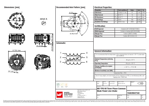
Dimensions: [mm]123456detail A1A744839047160Test Setup:744839047160744839047160T e m p e r a t u r eT T T 744839047160Cautions & Warnings:The following conditions apply to all goods within the product series of WE-TPBHV of Würth Elektronik eiSos GmbH & Co. KG:General:• This electronic component is designed and manufactured for use in general electronic equipment.•Würth Elektronik must be asked for written approval (following the PPAP procedure) before incorporating the components into any equipment in fields such as military, aerospace, aviation, nuclear control, submarine, transportation (automotive control, train control, ship control), transportation signal, disaster prevention, medical, public information network, etc. where higher safety and reliability are especially required and/or if there is the possibility of direct damage or human injury.•Electronic components that will be used in safety-critical or high-reliability applications, should be pre-evaluated by the customer. •The component is designed and manufactured to be used within the datasheet specified values. If the usage and operation conditions specified in the datasheet are not met, the wire insulation may be damaged or dissolved.•Do not drop or impact the components, the component may be damaged.•Würth Elektronik products are qualified according to international standards, which are listed in each product reliability report. Würth Elektronik does not warrant any customer qualified product characteristics beyond Würth Elektroniks’ specifications, for its validity and sustainability over time.•The responsibility for the applicability of the customer specific products and use in a particular customer design is always within the authority of the customer. All technical specifications for standard products also apply to customer specific products.Product specific:Soldering:•The solder profile must comply with the technical product specifications. All other profiles will void the warranty.•All other soldering methods are at the customers’ own risk.Cleaning and Washing:•Washing agents used during the production to clean the customer application might damage or change the characteristics of the wire insulation, marking or plating. Washing agents may have a negative effect on the long-term functionality of the product. Potting:•If the product is potted in the customer application, the potting material might shrink or expand during and after hardening. Shrinking could lead to an incomplete seal, allowing contaminants into the core. Expansion could damage the components. We recommend a manual inspection after potting to avoid these effects.Storage Conditions:• A storage of Würth Elektronik products for longer than 12 months is not recommended. Within other effects, the terminals may suffer degradation, resulting in bad solderability. Therefore, all products shall be used within the period of 12 months based on the day of shipment.•Do not expose the components to direct sunlight.•The storage conditions in the original packaging are defined according to DIN EN 61760-2.•The storage conditions stated in the original packaging apply to the storage time and not to the transportation time of the components. Packaging:•The packaging specifications apply only to purchase orders comprising whole packaging units. If the ordered quantity exceeds or is lower than the specified packaging unit, packaging in accordance with the packaging specifications cannot be ensured. Handling:•Violation of the technical product specifications such as exceeding the nominal rated current will void the warranty.•Applying currents with audio-frequency signals may result in audible noise due to the magnetostrictive material properties.•Due to heavy weight of the components, strong forces and high accelerations may have the effect to damage the electrical connection or to harm the circuit board and will void the warranty.•The temperature rise of the component must be taken into consideration. The operating temperature is comprised of ambient temperature and temperature rise of the component.The operating temperature of the component shall not exceed the maximum temperature specified.These cautions and warnings comply with the state of the scientific and technical knowledge and are believed to be accurate and reliable.However, no responsibility is assumed for inaccuracies or incompleteness.Würth Elektronik eiSos GmbH & Co. KGEMC & Inductive SolutionsMax-Eyth-Str. 174638 WaldenburgGermanyCHECKED REVISION DATE (YYYY-MM-DD)GENERAL TOLERANCE PROJECTIONMETHODHasA001.0012019-02-28DIN ISO 2768-1mDESCRIPTIONWE-TPB HV Three-Phase CommonMode Power Line Choke ORDER CODE744839047160SIZE/TYPE BUSINESS UNIT STATUS PAGEImportant NotesThe following conditions apply to all goods within the product range of Würth Elektronik eiSos GmbH & Co. KG:1. General Customer ResponsibilitySome goods within the product range of Würth Elektronik eiSos GmbH & Co. KG contain statements regarding general suitability for certain application areas. These statements about suitability are based on our knowledge and experience of typical requirements concerning the areas, serve as general guidance and cannot be estimated as binding statements about the suitability for a customer application. The responsibility for the applicability and use in a particular customer design is always solely within the authority of the customer. Due to this fact it is up to the customer to evaluate, where appropriate to investigate and decide whether the device with the specific product characteristics described in the product specification is valid and suitable for the respective customer application or not.2. Customer Responsibility related to Specific, in particular Safety-Relevant ApplicationsIt has to be clearly pointed out that the possibility of a malfunction of electronic components or failure before the end of the usual lifetime cannot be completely eliminated in the current state of the art, even if the products are operated within the range of the specifications.In certain customer applications requiring a very high level of safety and especially in customer applications in which the malfunction or failure of an electronic component could endanger human life or health it must be ensured by most advanced technological aid of suitable design of the customer application that no injury or damage is caused to third parties in the event of malfunction or failure of an electronic component. Therefore, customer is cautioned to verify that data sheets are current before placing orders. The current data sheets can be downloaded at .3. Best Care and AttentionAny product-specific notes, cautions and warnings must be strictly observed. Any disregard will result in the loss of warranty.4. Customer Support for Product SpecificationsSome products within the product range may contain substances which are subject to restrictions in certain jurisdictions in order to serve specific technical requirements. Necessary information is available on request. In this case the field sales engineer or the internal sales person in charge should be contacted who will be happy to support in this matter.5. Product R&DDue to constant product improvement product specifications may change from time to time. As a standard reporting procedure of the Product Change Notification (PCN) according to the JEDEC-Standard inform about minor and major changes. In case of further queries regarding the PCN, the field sales engineer or the internal sales person in charge should be contacted. The basic responsibility of the customer as per Section 1 and 2 remains unaffected.6. Product Life CycleDue to technical progress and economical evaluation we also reserve the right to discontinue production and delivery of products. As a standard reporting procedure of the Product Termination Notification (PTN) according to the JEDEC-Standard we will inform at an early stage about inevitable product discontinuance. According to this we cannot guarantee that all products within our product range will always be available. Therefore it needs to be verified with the field sales engineer or the internal sales person in charge about the current product availability expectancy before or when the product for application design-in disposal is considered. The approach named above does not apply in the case of individual agreements deviating from the foregoing for customer-specific products.7. Property RightsAll the rights for contractual products produced by Würth Elektronik eiSos GmbH & Co. KG on the basis of ideas, development contracts as well as models or templates that are subject to copyright, patent or commercial protection supplied to the customer will remain with Würth Elektronik eiSos GmbH & Co. KG. Würth Elektronik eiSos GmbH & Co. KG does not warrant or represent that any license, either expressed or implied, is granted under any patent right, copyright, mask work right, or other intellectual property right relating to any combination, application, or process in which Würth Elektronik eiSos GmbH & Co. KG components or services are used.8. General Terms and ConditionsUnless otherwise agreed in individual contracts, all orders are subject to the current version of the “General Terms and Conditions of Würth Elektronik eiSos Group”, last version available at .Würth Elektronik eiSos GmbH & Co. KGEMC & Inductive SolutionsMax-Eyth-Str. 174638 WaldenburgGermanyCHECKED REVISION DATE (YYYY-MM-DD)GENERAL TOLERANCE PROJECTIONMETHODHasA001.0012019-02-28DIN ISO 2768-1mDESCRIPTIONWE-TPB HV Three-Phase CommonMode Power Line Choke ORDER CODE744839047160SIZE/TYPE BUSINESS UNIT STATUS PAGE。
EDCS-7080 使用说明书V1.00(081231)

产品使用说明书
重庆新世纪电气有限公司
版本声明
版权所有:重庆新世纪电气有限公司 本技术说明书适用于以下版本的保护程序: EDCS-7080 微机小电流接地选线装置版本 V1.00。
序号 1 2 3 4 5 6 7 8 9 10
片和器件。 请使用合格的测试仪器和设备对装置进行试验和检测。 装置如出现异常或需维修,请及时与本公司服务热线联系。
NEW CENTURY-RELAYS
EDCS-7080 微机小电流接地选线装置使用说明书
目录
第一篇 装置技术说明................................................................................................................................ 1 1 概述 ..................................................................................................................................................... 1 1.1 应用范围 ............................................................................................................................................. 1 1.2 主要特点 ..................................................
XRC-200系列电容器保护装置说明书rev5

3.1 启动元件 ................................................................................................................................................ 7 3.2 过流保护 ................................................................................................................................................ 7 3.3 定时限过电压保护 ................................................................................................................................ 7 3.4 低电压保护 ............................................................................................................................................ 7 3.5 零序电流保护 ........................................................................................................................................ 8 3.6 不平衡电压保护 .................................................................................................................................... 9 3.7 不平衡电流保护 .................................................................................................................................... 9 3.8 桥差电流保护 ........................................................................................................................................ 9 3.9 差电压保护 ............................................................................................................................................ 9 3.10 过负荷保护 .......................................................................................................................................... 10 3.11 TV断线判别......................................................................................................................................... 10 3.12 控制回路断线功能 .............................................................................................................................. 10 3.13 低压自投 .............................................................................................................................................. 11
J-Link Rev 3.0 说明书
J-Link用户手册版本:Rev3.02007-09J-Link用户手册 Rev 3.0目录一、J-Link ARM JTAG仿真器简介二、J-LINK驱动安装三、J-LINK在各个主流开发环境下的设置四、J-FLASH ARM使用设置五、F.A.Q附录一、使用jlink的GDBserver附录二、J-Flash ARM命令行使用说明附录三、V6版本J-Link的特点和SWD使用说明J-Link用户手册 Rev 3.0版本更新说明Rev3.0:增加了附录三,主要介绍 V6版本的特点和SWD使用说明,2007-09更新Rev2.1:增加了命令行使用说明做为附录二,2007-05更新。
Rev2.0:添加了GDBserver的使用指南作为附录一,2006年10月更新。
Rev1.6a:修改了下载速度的错误,更新了器件支持,改动了一些地方的排版格式Rev1.6:添加IAR下使用XLINK进行FLASH下载的注意事项Rev1.5:添加KEIL下Utilities下的设置截图,2006-08升级Rev1.4:修正部分文字错误,添加速度测试截图,添加J-FLASH ARM新特性说明,2006-07升级Rev1.3a:增加F.A.Q,2006-06-07升级Rev1.3:增加F.A.Q,2006-06-04升级Rev1.2:增加J-FLASH ARM的操作说明,2006-06-02升级Rev1.0:原始版本,2006-06-01完成J-Link用户手册 Rev 3.0一、J-Link ARM JTAG仿真器简介J-Link是SEGGER公司为支持仿真ARM内核芯片推出的JTAG仿真器。
配合IAR EWARM,ADS,KEIL,WINARM,RealView等集成开发环境支持所有ARM7/ARM9内核芯片的仿真,通过RDI接口和各集成开发环境无缝连接,操作方便、连接方便、简单易学,是学习开发ARM 最好最实用的开发工具。
高密度设计适用的耐用抗干扰小型电阻器系列说明书
59MetalShaft RotaryPotentiometers SlidePotentiometers Multi Control Devices SensorsInsulatedShaft Hollow Type KnobOperating9mm Size Insulated Shaft Snap-in TypeRK09K/RK09D SeriesCompact type potentiometer with 9.8mm width is ideal for designing high density sets.Typical SpecificationsItemsTotalresistance tolerance Single-unit 20 30 50V AC 20V DC50V AC for AC only RK09K: 280 5 RK09D: 300 5280 5 1 to 8mN m 5,000cycles10,000cycles 10 to 70Dual-unit Single-unit Dual-unit Single-unit Dual-unitMaximum operating voltage Totalrotational angleRotational torqueOperating lifeOperating temperature rangeSpecificationsClosed structure improves dust and flux resistance.FeaturesFor various types of control in mini component stereos, portable audio, speaker systems and various audio equipmentFor controlling mixing consoles and electronic musical instruments For controlling flat panel TVs, game consoles, copy machines and refrigerators (temperature control)ApplicationsInsulated Shaft PotentiometerSingle-unitDual-unitResistancetaperNumber ofresistorelementsSingle-unit20V DCDual-unitNot applicableto DCMountingdirectionVerticaltypeHorizontaltypeH 6.5mmHorizontaltypeH 10mmShafttypeFlatKnobDriverLengthof the shaftmm1520253015203015201520302025302530201525301520152025CenterdetentWithWithoutTotalresistancek105105010201B15A1BTotalrotationangle280 5300 5280 5WithoutWithWithoutWithWithoutWithCollarSleeve typeProducts No.RK09K113004URK09K1130AU2RK09K1130A6SRK09K1130AJ3RK09K1130ACMRK09K1130ACLRK09K1130AAURK09K1130AH1RK09K1130BM4RK09K1130A8GRK09K1130A5RRK09K1130081RK09K1130A70RK09K1130AP5RK09K1130AV7RK09K1110A2SRK09K1110AK4RK09K1110AH8RK09K1110B1VRK09K1110A0JRK09K11100E9RK09K1110B1RRK09K1110B26RK09D1130C1BRK09D1130C2PRK09D1130A1LRK09D1130A1NRK09D1130C3WRK09D1130C3CRK09D113000FRK09D1110C0RRK09K12C0A19RK09K12C0A2SRK09K12C0A8GRK09K12C0D0URK09K12C0A8KRK09K12A0A2KRK09K12A0A6RRK09K12A0B0WMinimumpacking unitpcs.100DrawingNo.278156431012911 Recommended Products ListRefer to P.64for product varieties.Refer to P.78for product specifications.Products other than those listed in above recommended product are also available.Please contact us for details.NoteVerticaltypeVerticaltypeHorizontaltypeH 10mmHorizontaltypeH 6.5mmFlatFlatKnobWithWithWithWithoutWithoutWithout510510205105010505020105050101015A1B15A1B15A60MetalShaftRotaryPotentiometersSlidePotentiometersMulti ControlDevicesSensorsInsulatedShaftHollowTypeKnobOperating9mm Size Insulated Shaft Snap-in Type RK09K/RK09D SeriesInsulated Shaft Potentiometer61DimensionsHorizontal type with collar Single-shaft, single-unit Terminal Layout/Circuit DiagramSingle-unitDimensionsNo.PhotoStylePC board mountinghole dimensions Viewed from mounting sideUnit:mm5678Vertical type RK09K1136.80.84020ø69.87.40.81235.576.53.8 5.922.4(1.6)3217.40.89.85.550°LM 100.83.86.85.922.4R ø64.5R 762015LM 319.85.5240LM (0.8)(6.8)R ø6776302015LM 3.83.226R Mounting surface(The edge of the frame)52.58.21.83.3T 1.62.13-ø1h o l es32152.58.21.83.32.13-ø1 h o l e s 321T 1.63-ø1h o l es72.12.51.8510.610.61.82.553–ø1 h o l e s2.17Horizontal type RK09K111Horizontal type RK09K111Single-shaft, single-unit Teriminal Layout/Circuit DiagramSingle-unit321213123Vertical type RK09K113762015LM R R LM 9.81233.23.86.8 0.8ø65.562Mounting surfaceThe edge of the frameShaft shown in full CCW position.40 62Metal Shaft RotaryPotentiometers SlidePotentiometers Multi Control Devices SensorsInsulated Shaft Hollow Type KnobOperating9mm Size Insulated Shaft Snap-in Type RK09K/RK09D SeriesInsulated Shaft PotentiometerInsulated Shaft Potentiometer9mm Size Insulated Shaft Snap-in Type RK09K/RK09D Series63Metal ShaftRotaryPotentiometers SlidePotentiometers Multi Control Devices SensorsInsulated Shaft Hollow Type KnobOperatingPC board mounting hole dimensionsViewed from mounting sideTerminal Layout/Circuit DiagramDual-unitTapers 15A, 1B, 3B31221 3231123112233Tapers 15CDimensionsNo.PhotoStyleUnit:mm91011120.86.53.82.423.2ø64.56.89.850˚0.87.45.5Shaft shown in full CCW positionR 1LM 10.84.5ø63.83.26.8265.59.850˚Shaft shown in full CCW positionR 1LM 1576.53.82.423.220ø64.56.89.850˚0.87.45.5Shaft shown in full CCW position54.5ø63.83.26.8265.59.850˚Shaft shown in full CCW positionR 1LM 11.858.22.55-ø1h o l esT 1.63.32.52.15-ø1 ho l e s52.51.810.62.572.11.858.22.55-ø1 h o l es2.53.32.12.175-ø1 h o l e s 52.52.510.61.8Horizontal type RK09K12AVertical type RK09K12CSingle-shaft, dual-unit Horizontal type with collar RK09K12AVertical type with collar RK09K12C152067LM 1R 125301212LM 1R 11520673012LM 1R 1312213 2311112223339mm Size Insulated Shaft Snap-in Type Potentiometer64Metal Shaft RotaryPotentiometers SlidePotentiometers Multi Control Devices SensorsInsulatedShaft Hollow Type KnobOperatingRefer to P.65, 211 for resistance taper.Product VarietiesIn addition to the recommended products, the following specifications can also be accommodated.Total Resistance VarietyTotal resistance k5102050100200Resistance TaperShaft VarietyResistance taper15A1B3B15CNumber of resistor elementsSingle-unitDual-unitStyleShaft typeShaft colorBlackGray 15,20,25 Black 30BlackGray 20,25 Black 30BlackKnob varietyKnob type 6Detail dimensionsLM 1LM 1Mounting surfaceHorizontal typeVertical type ø640 Teeth knurlShaft shown atcenter positionR 1Screw-driver adjustment typeø640 Teeth knurlShaft shown at center positionR 1Flat typeø64.550˚Shaft shown in full CCW positionR 1Flat typeø64.560˚Shaft shown in full CCW positionR 1Flat type4.550˚Shaft shown in CCW positionø6R 1Flat typeø64.560˚Shaft shown in full CCW positionR 1Flat type4.550˚R 1ø6Shaft shown in full CCW positionFlat type4.550˚R 1ø6Shaft shown in CCW positionMounting surfaceLM 1LM 1With collar LM 1LM 1Mounting surfaceHorizontal typeVertical typeMounting surfaceLM 1LM 1With collarLM 1R 1156207257307LM 1R 115620725123012LM 1R 115620725123012LM 1R 120725123012LM 1R 120725123012LM 1R 115620725123012LM 1R 120725123012LM 1R 19.5156207Unit:mmmarked are specifications recommended by ALPS.Note1009080706050403020100100908070605040302010Rotation travel (%) Term."1"Term."3"O u t p u t v o l t .a c r o s s t e r m .1-2I n p u t v o l t . a c r o s s t e r m . 1-3G 100 (%)B (1B )J JA (15A )1009080706050403020100102030405060708090O u t p u t v o l t .a c r o s s t e r m .2-3I n p u t v o l t . a c r o s s t e r m . 1-3100C (15C )G100 (%)JRotation travel (%) Term."1"Term."3"J Orders Other Than Recommended ProductsWhen ordering product varieties that are not listed in the Recommended Product list, please speficy by referring to the below example.Sample Part NumberR K 09K 1130F 20C 0B 103Detent Code C0C1Center detentWithout WithModel type Code K111K113Model type280 single-unit horizontal type H 6.5D111300 single-unit horizontal type H 10D113300 single-unit vertical typeK12A 280 dual-unit horizontal type H 6.5K12C280 dual-unit vertical type280 single-unit vertical typeShaft type Code F Shaft typeFlat Code XShaft type DriverKKnobLength of the shaft LM 1 mm Code 15Length of theshaft 152020Code2530Length of theshaft2530Resistance taperCode A BResistance taper15A 1BResistance taper15C Code C 3BVTotal resistance Code 502103203Total resistancek Ω51020Total resistancek Ω50100Code 5031042002041.RK09D comes with a collar.2.The recommended specification for RK09K does not include a collar. For collar requirements please indicate separately.3.marked are specifications recommended by ALPS.NotesAll RK09D types are single-ganged.For other horizontal type mount height requirements,please indicate separately. 20, 25 and 30 are the only available RK09D types.,15 and 20 are the only available models in the driver shape. 1B is a recommended specification for single-unit.3B is a recommended specification for dual-unit.All RK09D types are only available in flat format.B:For tone & general V:For vol.65Metal Shaft RotaryPotentiometers SlidePotentiometers Multi Control Devices SensorsInsulated Shaft Hollow Type Knob Operating9mm Size Insulated Shaft Snap-in Type PotentiometerInsulated Shaft Potentiometers78。
通信用小微电源技术规范

通信用小微电源技术规范中国移动通信集团浙江有限公司通信用小微电源技术标准版本号:1.0.0中国移动通信集团浙江有限公司规划技术部二零一五年十二月目录1.范围 (1)2.规范性引用文件 (1)3.术语、定义和缩略语 (5)3.1.小微站点53.2.换流设备(单元)53.3.一体式53.4.模块化拼装式63.5.绝缘监测64.产品的组成和分类 (6)4.1.产品组成64.2.产品结构64.2.1.一体式产品结构 (7)4.2.2.模块化拼装式产品结构 (8)4.3.产品规格95.技术要求 (9)5.1.环境条件95.1.1.温度范围 (10)5.1.2.相对湿度范围 (10)5.1.3.大气压力 (10)5.1.4.冲击和振动 (10)5.2.系统外观与机械结构115.2.1.外观 (11)5.2.2.机械结构 (11)5.2.3.防护等级 (11)5.3.系统技术要求 115.3.1.系统容量 (11)5.3.2.系统输入 (12)5.3.3.系统输出 (12)5.3.3.1. -48V直流输出 (12)5.3.3.2. 280V直流输出 (12)5.3.4.系统并机工作性能 (13)5.3.5.系统峰-峰值杂音电压 (14)5.3.6.系统电压降 (14)5.3.7.温度系数 (14)5.3.8.保护功能 (14)5.3.8.1 .交流输入过、欠电压 (14)5.3.8.2. 直流输出过、欠电压保护 (15)5.3.8.3 .直流输出电流限制或输出功率限制功能 (15)5.3.8.4. 直流输出过流及短路保护 (15)5.3.8.5. 蓄电池过压、欠压、过流保护 (16)5.3.8.6.熔断器(或断路器)保护 (16)5.3.8.7.温度过高保护 (16)5.3.8.8.防雷性能 (16)5.3.8.9.保护接地性能 (17)5.3.9.输入、输出接口要求 (17)5.3.10.蓄电池管理功能195.3.11.通讯接口195.3.12.系统监控要求205.3.12.1总体要求 (20)5.3.12.2告警性能 (20)5.3.13.安全要求215.3.13.1绝缘电阻 (21)5.3.13.2抗电强度 (21)5.3.14.功率模块在线插拔功能225.3.15.电磁兼容225.3.16.材料阻燃性能235.3.17.系统噪声235.3.18.系统可靠性235.448V整流设备(单元)技术要求 245.4.1输入电压变动范围 (24)5.4.2交流输入频率变动范围 (24)5.4.3交流输入电压波形畸变率 (25)5.4.4交流输入功率因数 (25)5.4.5交流输入电流总谐波失真度 (25)5.4.6交流输入主电路接头间的相序和极性排列 (26)5.4.7源效应(电网调整率) (26)5.4.8开关机过冲幅度 (26)5.4.9启动冲击电流(浪涌电流) (26)5.4.10软启动时间275.4.11直流输出电压可调节范围275.4.12负载效应(负载调整率) 275.4.13负载效应恢复时间(动态响应) 275.4.14效率285.4.15接触电流285.4.16防雷性能295.5280V变换设备(单元)技术要求 295.5.1输入电压范围 (29)5.5.2开关机过冲幅度 (29)5.5.3启动冲击电流(浪涌电流) (30)5.5.4软启动时间 (30)5.5.5负载效应(负载调整率) (30)5.5.6负载效应恢复时间(动态响应) (30)5.5.7效率 (31)5.5.8防雷性能 (31)5.6蓄电池设备(单元)技术要求 315.7产品污染控制325.8包装运输贮存要求325.8.1包装要求 (32)5.8.2运输贮存要求 (32)6试验方法 (32)6.1试验环境条件326.2试验前准备336.3交流输入电压变动范围试验346.4输入频率变动范围试验346.5输入电压波形畸变率试验356.6输入功率因数试验356.7输入电流总谐波失真度试验356.8输入主电路接头间的相序和极性排列检查 (36)6.9整流设备试验 366.1048V直流输出电压可调节范围试验366.11稳压精度试验366.12系统杂音电压试验386.13直流配电部分电压降试验396.14输出分路要求396.15并联工作性能试验406.16监控性能试验416.17源效应(电网调整率)416.18温度系数试验426.19负载效应恢复时间(动态响应)试验446.19.1试验电路446.19.2试验方法与步骤456.20开关机过冲幅度试验456.21启动冲击电流(浪涌电流)试验466.22软启动时间试验476.23系统外观与机械结构检查476.24效率试验476.25系统音响噪声试验496.26交流输入过、欠电压保护试验496.27直流输出过、欠电压保护试验506.28直流输出电流限制或输出功率限制功能试验 (50)6.29直流输出过流及短路保护试验506.30蓄电池欠压保护试验516.31熔断器(或断路器)保护试验516.32温度过高保护试验526.33防雷性能试验526.33.1单相输入电源设备的纵向冲击实验。
【机电说明书】四方CSS-100BEFV2数字式安全稳定控制装置技术说明
1.1 适用范围...........................................................................................................................................1 1.2 装置主要特点...................................................................................................................................1
2 技术条件 ...................................................................................................................................................3
3.1 装置结构及配置 ...............................................................................................................................5 3.2 装置插件及接线说明 .......................................................................................................................9
目
录
第一篇 装置的技术说明................................................................................................................................1
微小电子零件说明书

050-5982 R e v D 3-2008Microsemi Website - CAUTION: These Devices are Sensitive to Electrostatic Discharge. Proper Handling Procedures Should Be Followed .MAXIMUM RATINGSAll Ratings: T C = 25°C unless otherwise speci fi ed.STATIC ELECTRICAL CHARACTERISTICSSymbol BV DSS V DS (ON)I DSS I GSS g fs V isolation V GS (TH)Characteristic / Test ConditionsDrain-Source Breakdown Voltage (V GS = 0V, I D = 250 μA) On State Drain Voltage 1 (I D (ON) = 15A, V GS = 10V)Zero Gate Voltage Drain Current (V DS = 1000V, V GS = 0V)Zero Gate Voltage Drain Current (V DS = 800V, V GS = 0V, T C = 125°C)Gate-Source Leakage Current (V GS = ±30V, V DS = 0V)Forward Transconductance (V DS = 25V, I D = 15A)RMS Voltage (60Hz Sinewave from terminals to mounting surface for 1 minute)Gate Threshold Voltage (V DS = V GS , I D = 50mA)MIN TYP MAX10007.59 40 1000±400 5.57TBD3 5UNIT VoltsμAnAmhos VoltsSymbol V DSS I D V GS P D T J ,T STGT LParameterDrain-Source VoltageContinuous Drain Current @ T C = 25°C Gate-Source VoltageTotal Device Dissipation @ T C = 25°COperating and Storage Junction Temperature Range Lead Temperature: 0.063" from Case for 10 Sec.ARF1501 1000 30 ±30 1500-55 to 175300UNIT Volts Amps Volts Watts °CRF POWER MOSFETN -CHANNEL ENHANCEMENT MODE250V 750W 40MHzThe ARF1501 is an RF power transistor designed for very high power scienti fi c, commercial, medical and industrialRF power generator and ampli fi er applications up to 40 MHz.• Speci fi ed 250 Volt, 27.12 MHz Characteristics: Output Power = 750 Watts. Gain = 17dB (Class C) Ef fi ciency > 75%• High Performance Power RF Package.• Very High Breakdown for Improved Ruggedness.• Low Thermal Resistance.• Nitride Passivated Die for Improved Reliability.ARF1501THERMAL CHARACTERISTICSSymbol R θJC R θJHSCharacteristic (per package unless otherwise noted)Junction to CaseJunction to Sink (Use High Ef fi ciency Thermal Joint Compound and Planar Heat Sink Surface.)MIN TYP MAX0.100.16UNIT °C/WVolts050-5982 R e v D 3-2008Microsemi reserves the right to change, without notice, the speci fi cations and information contained herein.DYNAMIC CHARACTERISTICSARF1501Symbol C iss C oss C rss t d(on)t r t d(off)t fCharacteristic Input Capacitance Output CapacitanceReverse Transfer Capacitance Turn-on Delay Time Rise TimeTurn-off Delay Time Fall TimeTest ConditionsV GS = 0V V DS = 200V f = 1 MHz V GS = 15V V DD = 500V I D = I D[Cont.] @ 25°CR G = 1.6 ΩMINTYPMAX5400 6500 300 400 125 160 8 5 2513UNITpFns FUNCTIONAL CHARACTERISTICSSymbol G PS ηΨTest Conditions f = 27.12 MHz V GS = 0V V DD = 250VP out = 750WNo Degradation in Output PowerCharacteristicCommon Source Ampli fi er Power Gain Drain Ef fi ciencyElectrical Ruggedness VSWR 10:1MIN TYP MAX 15 17 7075UNIT dB %1Pulse Test: Pulse width < 380 μS, Duty Cycle < 2%.1000I D , D R A I N C U R R E N T (A M P E R E S )V DS , DRAIN-TO-SOURCE VOLTAGE (VOLTS)Figure 3, Typical Maximum Safe Operating Area1ms10ms 100usPer transistor section unless otherwise speci fi ed.100msC A P A C I T A N C E (p f )V DS , DRAIN-TO-SOURCE VOLTAGE (VOLTS)Figure 1, Typical Capacitance vs. Drain-to-Source VoltageV GS , GATE-TO-SOURCE VOLTAGE (VOLTS)Figure 2, Typical Transfer CharacteristicsI D , D R A I N C U R R E N T (A M P E R E S )= -55°C= +125°C= +25°C050-5982 R e v D 3-2008HAZARDOUS MATERIAL WARNINGThe ceramic portion of the device between leads and mounting surface is beryllium oxide, BeO. Beryllium oxide dust is toxic when in-haled. Care must be taken during handling and mounting to avoid damage to this area These devices must never be thrown away with general industrial or domestic waste.Thermal Considerations and Package Mounting:The rated 1500W power dissipation is only avail-able when the package mounting surface is at 25°C and the junction temperature is 200°C. The thermal resistance between junctions and case mounting surface is 0.12°C/W. When installed, an additional thermal impedance of 0.1°C/W between the package base and the mounting surface is typi-cal. Insure that the mounting surface is smooth and flat. Thermal joint compound must be used to reduce the effects of small surface irregularities. The heatsink should incorporate a copper heat spreader to obtain best results.The package is designed to be clamped to a heatsink. A clamped joint maintains the required mounting pressure while allowing for thermal ex-pansion of both the device and the heat sink. A simple clamp, and two 6-32 (M3.5) screws can pro-vide the minimum 125lb required mounting force. T = 12 in-lb.Table 1 - Typical Class AB Large Signal Impedance -- ARF1501F (MHz)Z in (Ω)Z OL (Ω)2.013.5274010.6 -j 12.20.5 -j 2.70.22 -j 0.80.2 +j .1231 -j 4.715.6 -j 166.2 -j 12.63.1 -j 9.4Z in - Gate shunted with 25Ω I DQ = 100mAZ OL - Conjugate of optimum load for 750 Watts output at V dd = 250VARF1501Z qJ C , T H E R M A L I M P E D A N C E (°C /W )0.140.120.100.080.060.040.020T C , CASE TEMPERATURE (°C)Figure 4, Typical Threshold Voltage vs Temperature V DS , DRAIN-TO-SOURCE VOLTAGE (VOLTS)Figure 5, Typical Output Characteristics1.151.101.051.000.950.900.850.800.75 -50 -25 0 25 50 75 100 125 150I D , D R A I N C U R R E N T (A M P E R E S )V G S (t h ), T H R E S H O L D V O L T A G E (N O R M A L I Z E D )RECTANGULAR PULSE DURATION (SECONDS)Figure 6, Maximum Effective Transient Thermal Impedance, Junction-to-Case vs. Pulse Duration050-5982 R e v D 3-2008C1, C7,C8, C11 .1uF 250V ceramic chip C2, C12 ARCO 465 75-380pF mica trimmer C3 4700pF ATC700BC4, C9-C11 8200pF 500V NPO ceramic C5 - C6 150pF ATC 700B L1 90 nH 4t #18 0.25"d .25"lL2 175 nH - 3t #10 .75" dia .75" l L3 2uH - 22t #24 enam. .312" dia.L4 500nH 2t on 850u .5" bead R1-R3 1k Ω 1/4WTL1 .112" x 1.2" (50 Ω) StriplineARF1501 -- 27.12 MHz Test CircuitParts placement1:1 pcb artwork。
小型无线电路板用户指南说明书

1 23 4 5 67 89 1011 1213 14Console Action Console Response Console Action Console ResponseAT AT<0x0d><0x0a><0x0d><0x0a>OK<0x0d><0x0a>AT<0x0d><0x0a><0x0d><0x0a>OK<0x0d><0x0a>Attention.AT+RST AT+RST<0x0d><0x0a><0x0d><0x0a>OK<0x0d><0x0a>AT+RST<0x0d><0x0a><0x0d><0x0a>OK<0x0d><0x0a>Reset the unit.AT+GMR<0x0d><0x0a>Ready<0x0d><0x0a>0<0x0d><0x0a>Ready<0x0d><0x0a>Retrieving the firmware version Id.AT+CWMODE=?AT+CWMODE?AT+CWMODE=<mode>AT+GMR<0x0d><0x0a>150900AT+GMR<0x0d><0x0a>150900Setting operation mode.1 - client2 - Access Point3 - Client and Access PointThe access point functionality does not have DHCP function and it has only minimunfunctionalities.However, it will assign IP address to client and there is not way to do manual IP, manualDNS and other advance IP functionality. This unit only provide minimal functionality.AT+ CWJAP = <ssid>,< pwd >AT+ CWJAP?AT+CWJAP="ssid","abcdefgh"<0x0d><0x0a><0x0d><0x0a>OK<0x0d><0x0a>AT+CWJAP="ssid","abcdefgh"<0x0d><0x0a><0x0d><0x0a>OK<0x0d><0x0a>Joining a network or just an access point.AT+CWLAP AT+CWLAP<0x0d><0x0a><0x0d><0x0a>+CWLAP:(0,"",0)<0x0d><0x0a>CWLAP(4,"ssid",-76)<0x0d><0x0a>CWLAP:(3,"another",-80)<0x0d><0x0a>AT+CWLAP<0x0d><0x0a><0x0d><0x0a>+CWLAP:(0,"",0)<0x0d><0x0a>CWLAP(4,"ssid",-76)<0x0d><0x0a>CWLAP:(3,"another",-80)<0x0d><0x0a>Retrieving the list of visible network.AT+CWQAP AT+CWQAP<0x0d><0x0a><0x0d><0x0a>OK<0x0d><0x0a>AT+CWQAP<0x0d><0x0a><0x0d><0x0a>OK<0x0d><0x0a>Disconnect from current network connection.AT+ CWSAP= <ssid>,<pwd>,<chl>, <ecn>AT+CWSAP?AT+CWSAP="ESP_9945B5","abcdefgh",11,0<0x0d><0x0a><0x0d><0x0a>OK<0x0d><0x0a>Since security is set to 0(open), the password is notbeing used.Seting up access point ssid, password, RF channel and security scheme.The following is the security scheme:0 - Open. No security.1 - WEP.2 - WPA_PSK3 - WPA2_PSK4 - WPA_WPA2_PSKAT+CWLIF<0x0d><0x0a>192.168.4.100<0x0d><0x0a>OK<0x0d><0x0a>AT+CWLIF<0x0d><0x0a>192.168.4.100<0x0d><0x0a>OK<0x0d><0x0a>Retrieving list of assigned IP addresses.AT+ CIPSTATUS AT+CIPSTATUS<0x0d><0x0a>STATUS:3<0x0d><0x0a>+CIPSTATUS:0,"TCP", "10.1.10.20",23,0<0x0d><0x0a>OK<0x0d><0x0a>AT+CIPSTATUS<0x0d><0x0a>STATUS:3<0x0d><0x0a>+CIPSTATUS:0,"TCP","192.168.4.100",1624,1<0x0d><0x0a>OK<0x0d><0x0a>Retrieving the current connection as socket client or socket server.AT+CIPSTART=?AT+CIPSTART= <type>,<addr>,<port> (AT+CIPMUX=0)AT+CIPSTART= <id><type>,<addr>,<port> (AT+CIPMUX=1)AT+CIPSTART="TCP","10.1.10.20",23<0x0d><0x0a><0x0d><0x0a>OK<0x0d><0x0a>AT+CIPSTART="TCP","10.1.10.20",23<0x0d><0x0a><0x0d><0x0a>OK<0x0d><0x0a>Connecting to socket server (TCP or UDP). Connecting using domain name only workingwith public domain name such as but not the name of the clients of thelocal router or access points since the DNS servers are built-in into the firmware of theunit as follow: 28.4.192.168,4.255.26.2 and 2.64.31.1.The access point IP address is fixed at 192.168.4.1 and the network mask is fixed at255.255.255.0.More detailed info can be retrieved by executing 'ipconfig /all' in Windows.AT+CIPMUX=0AT+CIPMUX=1Manual CommandCopyright® 2014 EINFODEV, Inc. All rights reserved.15 16 17 181920 21 22AT+CIPSEND=<length> (AT+CIPMUX=0 & AT+CIPMODE=0)AT+CIPSEND= <id>,<length> (AT+CIPMUX=1 & AT+CIPMODE=0)AT+CIPSEND (AT+CIPMUX=0 & AT+CIPMODE=1)AT+CIPSEND=1<0x0d><0x0a>>AT+CIPSEND=0,1<0x0d><0x0a>>Sending by connection channel and by specific length.AT+CIPSEND=<length> is for AT+CIPMODE=0 and AT+CIPMUX=0.AT+CIPSEND=<channel>,<length> is for AT+CIPMODE=0 and AT+CIPMUX=1.Sending data without connection channel and specific length only working whenAT+CIPMODE=1 and AT+CIPMUX=0 and sending data using AT+CIPSEND=<length> willreset the unit.AT+CIPCLOSE AT+CIPCLOSE<0x0d><0x0a><0x0d><0x0a>OK<0x0d><0x0a>AT+CIPCLOSE=0<0x0d><0x0a><0x0d><0x0a>OK<0x0d><0x0a>Close the socket connection.AT+CIFSR AT+CIFSR<0x0d><0x0a><0x0d><0x0a>10.1.10.26<0x0d><0x0a>AT+CIFSR<0x0d><0x0a><0x0d><0x0a>10.1.10.26<0x0d><0x0a>Retrieving the assigned IP address when the unit is connecting to a network.AT+ CIPMUX=<mode>AT+ CIPMUX?AT+CIPMUX=0<0x0d><0x0a><0x0d><0x0a>OK<0x0d><0x0a>AT+CIPMUX=1<0x0d><0x0a><0x0d><0x0a>OK<0x0d><0x0a>Setting single connection (AT+CIPMUX=0) or multi-channel connection (AT+CIPMUX=1). AT+ CIPSERVER= <mode>[,<port>] (AT+CIPMUX=1)AT+CIPSERVER=1,23<0x0d><0x0a><0x0d><0x0a>OK<0x0d><0x0a>AT+CIPSERVER=1,23<0x0d><0x0a><0x0d><0x0a>OK<0x0d><0x0a>Start at the specified port or stop the server.Default port is 333.<mode> is as follow:0 - close the socket server1 - open the socket serverAT+CIPMODE=<mode>AT+CIPMODE?AT+CWMODE=1<0x0d><0x0a><0x0d><0x0a>OK<0x0d><0x0a>AT+CWMODE=1<0x0d><0x0a><0x0d><0x0a>OK<0x0d><0x0a>Setting transparent mode (data from socket client will be send to the serial port as is) orconnection channel specific mode (+IPD,<connection channel>,<length>).Data sent from socket client will be broken into multiple unsolicited (+IPD,<connectionchannel>,<length>) segments.<mode> is as follow:0 - data received will be send to serial port with +IPD,<connection channel>,<length>format. (AT+CIPMUX=[0,1])1 - data received will be send to serial port as data stream. (AT+CIPMUX=0)AT+CIPSTO=<time>AT+CIPSTO?AT+CIPSTO=28800<0x0d><0x0a><0x0d><0x0a>OK<0x0d><0x0a>AT+CIPSTO=28800<0x0d><0x0a><0x0d><0x0a>OK<0x0d><0x0a>Setting the automatic socket client disconnection timeout from 1 to 28800 seconds dueto inactivities.Packetized data from the unit<0x0d><0x0a>+IPD,0,1:A<0x0d><0x0a>OK<0x0d><0x0a><0x0d><0x0a>+IPD,0,1:A<0x0d><0x0a>OK<0x0d><0x0a>Unsolicited data packet (+IPD,<connection channel>,<length>) .。
AVP100使用说明书
系统配置 系统配置如下所示。该图也说明了由一个 SVP、一个便携式设定显示屏、一个现场电流表和 一个齐纳式安全栅组成的一个本质安全系统的布局。 除连接至安全栅非本质安全侧的组件 之外,其它系统组件都必须由一个权威的测试机构进行认证。
图 S-1 本质安全型 SVP 的系统配置
iii 型号 AVP100/102-SVP3000 Alphaplus 智能阀门定位器
注
对用户有用的信息。
拆开包装
务必小心对待设备,防止任何损坏。 请确认包装中含有下列物品: • SVP3000 Alphaplus 智能阀门定位器
型号:AVP100 (1) / AVP102 (1) • 反馈杆 (1)和内六角螺钉 (2)。 • 用于反馈杆的六角扳手 (1) • 压力表 (选购) • 管接头 (选购) • 说明书 (选购)
第二章:安装
2-1 : SVP 装配 .......................................................................................................................................2-3 2-1-1: 安装 SVP 反馈杆 ...................................................................................................................2-3
C 2005!ᓀါ્!ᇊ!ۈཚჅᎌ
安全
安全注意事项
妥善的安装、正确的操作和安装后的维护对本智能型阀门定位器的安全使用都至关重要。 本说明书中提出的安全指示分为 警告 、注意 和 注 三种类型。
微电子PID控制器参数及说明
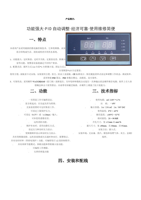
产品简介:功能强大·PID自动调整·经济可靠·使用维修简便一、特点本系列产品采用最新的微电脑控制技术,它和变频器、水泵组合即构成生活、消防或两者共用供水系统。
1、功能强大:定时换泵,定时开关机,定量泵巡查,附属小泵等功能,使整套设备能满足不同用户要求。
2、配置灵活:循环方式2-4台泵+1台附属小泵;固定方式1台变频泵+1-3台定量泵。
使用方便:面板表卡式安装,安装使用方便。
防尘、防水工业面板,CE标准设计。
简化键盘菜单式设定和调整工作状态,调试简单。
采用智能PID算法,PID参数自整定,高精度,高可靠性。
3、可靠性高:采用硬件WATCHDOG(看门狗)故障复位,另外每秒钟微机自动复位一次和输出状态硬件锁存电路,软件上引入容错概念和去干扰等算法。
内部带有屏蔽层隔离,在硬件上增强了抗干扰能力。
二、功能. 一至四泵工作可编程设定。
. 泵全软起动,以先起先停为原则。
. 无加泵需要时可定时换泵工作。
. 可设定上限保护压力。
. 可设定(0-5V)或(4-20mA)输入。
. 可补偿传感器误差。
. 远传消防功能。
. 锅炉补水时,采用动静压方式。
. 设定压力和实时压力显示。
. 变频器频率显示和实时压力显示。
. 具有变频器故障、远传表故障或欠压超时和水位、报警指示。
具有实时时钟(带掉电保护)功能。
可编程每日12段控制程序。
. 具有两种节能模式,休眠功能和带附属小泵功能。
. 可编程工作期限。
. 完善的密匙功能三、技术指标. 使用电源:AC 220V +15%. 功耗:< 6W. 触点容量:5A / 250 AC 5A / 30V DC. 使用温度:0°C ~ 40°C. 储存温度:-100°C ~ 85°C. 相对湿度:20 ~ 90 RH. 开孔尺寸:宽152mm高mm76。
. 最大尺寸:宽160mm,高80mm,深95mm。
. 安装方法:插入式。
AdderLink DV100 产品说明书

微焦点XJD-100(电子元器件)使用说明书
目录1 XJD-100型微焦点X射线电子元器件检测仪基本组成 (3)1.1基本组成 (5)2.咼频咼压X射线机 (5)2.1基本描述 (5)2.2构成 (6)2.3安全 (7)2.4设备使用 (9)2.5维护和保养 (10)3计算机图像处理 (11)4检测平台控制系统 (11)附件1原理图 (12)附件2原理图 (13)1、公司简介丹东奥龙射线仪器有限公司是我国射线仪器行业规模最大、技术力量最雄厚、综合实力最强的民营咼科技企业,中国射线仪器科研和生产基地。
奥龙射线是无损检测行业中唯一的高新技术企业,已通过 ISO9001:2000 国际质量体 系认证,被认定为辽宁省企业技术中心、 辽宁省软件企业, 辽宁省模范劳动关系和谐企业、辽宁省企事业知识产权试点单位,拥有进出口经营权。
公司座落于丹东市临港高新技术产业园区, 占地面积 3 万平方米,建筑面积 1.5万平 方米,具有先进的生产设备和检测设备。
奥龙主导产品:X 射线探伤机X 射线实时成像在线检测系统工业 CT 管道爬行器微焦点 X 射线检测仪奥龙射线的产品不仅填补了国内空白,而且 X 射线实时成像检测系统和微焦点 X 射 线检测仪先后被确定为国家高技术产业化示范工程项目;工业 CT 被国家列入“十一五” 重点发展规划; X 射线实时成像检测系统被列为国家重点新产品; X 射线探伤机、 X 射线 衍射仪等产品被国家及省授予优质产品奖和科技成果奖; 拥有多项国家专利和计算机软件 著作权;产品水平居国内领先地位, 并主导着国内市场。
中国发射的神舟载人飞船有多项 系统使用奥龙射线生产的 X 射线探伤设备进行无损检测获得成功,为中国航天事业发展 做出贡献。
“奥龙”产品荣获辽宁名牌产品称号。
奥龙射线营销网络经过多年的拓展, 已经在国内有了较高的市场占有率, 并不断向国 际市场发展。
产品远销美国、韩国、朝鲜、苏丹、马来西亚、印度、菲律宾、伊朗、泰国 等国家和地区。
- 1、下载文档前请自行甄别文档内容的完整性,平台不提供额外的编辑、内容补充、找答案等附加服务。
- 2、"仅部分预览"的文档,不可在线预览部分如存在完整性等问题,可反馈申请退款(可完整预览的文档不适用该条件!)。
- 3、如文档侵犯您的权益,请联系客服反馈,我们会尽快为您处理(人工客服工作时间:9:00-18:30)。
目录1XJD-100型微焦点X射线电子元器件检测仪基本组成 (3)1.1基本组成 (5)2.高频高压X射线机……………………………………………………………52.1 基本描述………………………………………………………………………52.2构成 (6)2.3安全 (7)2.4设备使用 (9)2.5维护和保养 (10)3计算机图像处理 (11)4检测平台控制系统………………………………………………………………11附件1原理图………………………………………………………………………12附件2原理图………………………………………………………………………131、公司简介丹东奥龙射线仪器有限公司是我国射线仪器行业规模最大、技术力量最雄厚、综合实力最强的民营高科技企业,中国射线仪器科研和生产基地。
奥龙射线是无损检测行业中唯一的高新技术企业,已通过ISO9001:2000国际质量体系认证,被认定为辽宁省企业技术中心、辽宁省软件企业,辽宁省模范劳动关系和谐企业、辽宁省企事业知识产权试点单位,拥有进出口经营权。
公司座落于丹东市临港高新技术产业园区,占地面积3万平方米,建筑面积1.5万平方米,具有先进的生产设备和检测设备。
奥龙主导产品:●X射线探伤机●X射线实时成像在线检测系统●工业CT●管道爬行器●微焦点X射线检测仪●X射线衍射仪●X射线荧光光谱仪●X射线晶体分析仪●X射线晶体定向仪●X射线管奥龙射线的产品不仅填补了国内空白,而且X射线实时成像检测系统和微焦点X射线检测仪先后被确定为国家高技术产业化示范工程项目;工业CT被国家列入“十一五”重点发展规划;X射线实时成像检测系统被列为国家重点新产品;X射线探伤机、X射线衍射仪等产品被国家及省授予优质产品奖和科技成果奖;拥有多项国家专利和计算机软件著作权;产品水平居国内领先地位,并主导着国内市场。
中国发射的神舟载人飞船有多项系统使用奥龙射线生产的X射线探伤设备进行无损检测获得成功,为中国航天事业发展做出贡献。
“奥龙”产品荣获辽宁名牌产品称号。
奥龙射线营销网络经过多年的拓展,已经在国内有了较高的市场占有率,并不断向国际市场发展。
产品远销美国、韩国、朝鲜、苏丹、马来西亚、印度、菲律宾、伊朗、泰国等国家和地区。
广泛应用于航空、航天、造船、汽车、压力容器、机械、冶金、铸造、石油管道、钢管、化工、电子、输变电、耐火材料、科技教育、大专院校、卫生等行业的无损检测需要。
2007年8月,奥龙射线与无损检测行业的全球领导厂商美国GE检测科技公司成功签约,进而奠定了奥龙射线在国际无损检测领域发展的地位。
奥龙射线注重人才培养,是一支拥有高尚厚重企业文化的优秀团队,已建成与世界接轨的现代化新厂区。
奥龙人始终以建设好射线基地为己任,做中国领先的射线仪器制造商和应用服务商,缔造一个永续昌盛的射线仪器科研和生产基地,是奥龙人永恒不变的追求!1.XJD-100型微焦点X射线电子元器件检测仪基本组成计算机图像处理系统高频高压X射线机检测平台控制系统注:(外形不断升级外形如有变化,恕不另行通知) 1.1、基本组成:1)高频高压X射线机2)计算机图像处理系统铅防护系统影像接收装置机械检测平台3)检测平台控制系统4)影像接收装5)机械检测平台6)铅防护系统2、高频高压X射线机2.1基本描述2.2 构成2.2.1 控制台2.2.2 X射线源组装体2.2.3 曝光自动接通控制装置2.2.4环境温度:10~40℃。
湿度:≤80%。
大气压强:70KPa∽106KPa2.2.5 电源条件:AC220V±10%.50HZ±1HZ.接地电阻:≤0.5Ω.输入功率:≥3kw.2.2.6基本参数主机功率:5kw.主机频率:40KHZ.Kv调整范围:30Kv~80Kv连续调整.MA调整范围:0~500µA连续调.整焦点尺寸:0.05mm2.3、安全性2.3.1、简介本手册的目是为从事放射工作的人员安全简便的使用放射设备提供使用指南。
本设备能够发射X射线,因此必须严格按照本手册所规定的安全使用规则使用,严禁用于其他本手册未提及的目的。
本系统必须由具备必要的放射防护知识并接受过必须的X线设备使用培训的人员使用,并严格遵守如下规则:·当设备出现电器或机械故障时,严禁使用;·当设备的报警装置或指示装置工作不正常时,严禁使用;·必须在得到生产厂的书面认可后方可对设备进行改动;·如果您想将本设备与其它设备、部件或模块配合使用,但与这些设备的兼容性不确定的情况下,最重要的是保证对周围环境及操作者没有危险。
在这种情况下,请咨询制造厂或有关方面的专家。
·和其它所有设备一样,本系统必须正确使用。
并需要按照本手册第4节设备维护和保养中所描述的进行定期检查和保养。
2.3.2系统机械安全性2.3.2.1 机械安全性·避免撞击任何障碍物。
·除非按照使用手册中描述的进行维修和保养,否则不要取下设备的保护外罩。
·确定设备将要连接的电源插座及输出符合本设备对电源的要求·严禁在存在爆炸危险性的房间内使用放射设备·注意不要将任何导电的液体泼洒在设备上·如果在使用中突然发生故障,迅速按下控制台上的急停按钮,以避免出现不需要的射线,使用完毕后关机2.3.2.2设备的保护接地为了操作者的安全,一定要将该设备及相关机架等良好接地2.3.3潜在的危险防电击保护是采用对所有金属部件接地的方式,因此须定期按照本手册第4节所描述的日常保养计划对设备接地状况进行检查2.3.4 信号及标志2.3.4.1信号及报警信息2.3.4.1.1表2.2 控制台上显示的信息人员联系Ld2灯点亮(检测板上) 在摄影中,施加于X线管的电压过高或有放电关机,再开机,进行曝光,如出现同样错误,请与技术服务人员联系Ld3灯点亮(检测板上) 在摄影中,施加于X线管的电压大于设置值的110%关机,再开机,进行曝光,如出现同样错误,请与技术服务人员联系Ld4灯点亮(检测板上)在摄影中,施加于X线管的电压过低或线路连接故障关机,再开机,进行曝光,如出现同样错误,请与技术服务人员联系摄影mA很低且不受调无灯丝加热电流关机,再开机,进行曝光,如出现同样错误,请与技术服务人员联系过热报警灯(3)点亮组合机头温度过高等待组合机头降温2.4.设备的使用2.4.1.电缆的连接将设备的相关电缆线按要求正确、牢固的连接好,检查无误后接通电源。
2.4.2开机为使系统能够使用,请遵照如下操作:·将控制台上的电源开关(14)打开·使用专用钥匙将控制台电源(1)打开2.4.3 X线曝光曝光前确认已经采取了必要的放射防护措施。
(关闭铅门)注意:不管选用何种曝光模式,当有X线发生时,控制台上的高压指示灯(2)会点亮,同时显示面板上Kv及mA窗口会显示当前的曝光条件2.4.3.1 曝光条件的调整·按下射线接通按钮(5)·分别旋转Kv及mA窗口右侧的调整旋钮(11)(9)至所需要的条件·按下5分钟限时切换按钮(7)注意:当累计照射达到5分钟时,设备会自动切断曝光,此时按下射线关断按钮(6),如需继续工作,按下5分钟限时清零按钮(4)同时进行上述操作即可。
·需要关断射线时,按下射线关断按钮(6)2.4.3.2曝光自动接通装置的连接将曝光自动接通传感器与控制台背面的曝光自动接通接口(18)连接。
2.4.3.3 X射线源组装体过热报警当X射线源组装体过热,控制台面板上报警灯(3)会点亮,此时应停止工作,待彻底散热后再继续工作。
注意:此报警表明X线管已处于相当高的温度状态,继续使用,会导致永久性损坏的可能性增加。
2.5. 维护和保养本用户手册仅涉及日常的维护和保养。
对于特殊的维修,或者是因为故障或更换器件,请参考技术手册。
2.5.1日常维护2.5.1.1一般建议放射设备需要定期进行检查和维护。
建议着重于保持良好的操作和安全性。
维护程序包括检查和预防性的内部查看,须由设备所有者参与,且必须由被授权的专门人士进行。
注意:在必须进行部件更换时,请尽量使用原厂部件,以保证设备的安全性。
2.5.1.2用户进行的检查用户必须对其操作人员进行培训,以便他们能够进行日常检查。
日常检查内容如下表所列:3.计算机图像处理系统3.1 计算机图像处理主要对X射线视频图像进行数字化处理、存储、放大、降噪、滤波、图像输出等。
它的主要组成有:计算机、显示器、图像采集卡、图像处理系统软件、刻录机、打印机等。
3.2软件主要功能:优异的操作性能;全面操作的独创性;功能压缩精心提炼使检测操作高效率;长期使用的稳定性。
动态图像采集;图像保存;图像降噪及滤化功能;多帧叠加降噪保存;调节参数自动保存;灰度拉伸变换;实时负片伪彩;实时无极放大/缩小;检测(面积、周长、角度、曲率);还原;停止;图片打印;报表打印;DVD刻录。
4.检测平台控制系统采用PLC控制使速度可调,有几何放大,平台沿X轴、Y轴运动。
检测平台有两种形式:一种是检测平台上可有夹件工装可作旋转;另一种是检测平台可左右移动。
以达到最佳的角度。
为了您的安全,请注意辐射!附件一:电气图附件二:电气图。
