LY5380-H中文资料
AM3KA538用户手册说明书
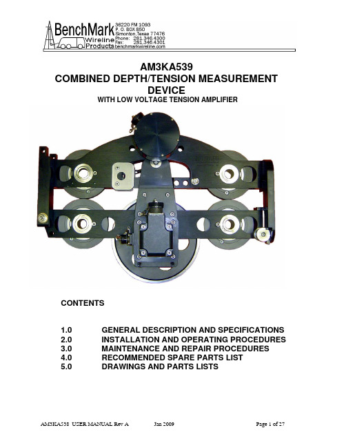
AM3KA539COMBINED DEPTH/TENSION MEASUREMENTDEVICEWITH LOW VOLTAGE TENSION AMPLIFIERCONTENTSDESCRIPTION AND SPECIFICATIONS1.0 GENERAL2.0 INSTALLATIONOPERATING PROCEDURESANDREPAIR PROCEDURES3.0 MAINTENANCEAND4.0 RECOMMENDED SPARE PARTS LIST5.0 DRAWINGS AND PARTS LISTS1.0 GENERAL DESCRIPTION AND SPECIFICATIONSThe BenchMark Measurement System AM3K measuring device combines in one compact, lightweight unit, both depth measurement and line tensionmeasurement capabilities. A single measuring wheel is used to drive anoptical encoder. An electronic load axle is used to measure line tension.MEASUREMENT1.1 DEPTHThe AM3K uses a single measuring wheel to measure the amount ofwireline moving to and from the borehole. The measuring wheel is coupled to an encoder that transmits electrical signals via a cable to the hoistman’spanel and/or logging computer representing cable travel. An independentlypowered encoder and display panel is used for back up depth indication.The hardened measuring wheel has a 2.0000 ft. (609.600 mm)circumference with a 3/8" groove. A spring mounted tension roller is used to hold the measuring wheel in contact with the wireline.Two guide rollers are used to properly hold the cable in line with themeasuring wheel. Wear blocks are also used to guide the cable and prohibit cable contact with the frame members. The frame members are anodized aluminum.6061-T6MEASUREMENT1.2 TENSIONThe AM3K uses an electronic load axle on the measuring wheel to measureline tension. Three wheels are used to create a force on the load axle normal to the axis of the wireline. To generate this force the wheel mounted on theload axle is offset from the other two slightly. This offset creates a slight bend in the cable.As wireline tension increases the small offset creates a correspondingbending force on the strain-gauged load axle. An electronic signal istransmitted via cable to the hoistman’s panel and/or logging computertension. A calibrate resistor is included in the load pin to wirelinerepresentingsend out a signal to calibrate the computer system.SPECIFICATIONS1.3 GENERAL13.6kglbs30WEIGHT:mm500 LENGTH:19.6”mm343 HEIGHT: 13.5”mm WIDTH: 8.2”208 CABLE BEND OVER TENSION WHEEL: < 10 DegreesMAXIMUM LINE TENSION: 10,000 lbs 4538 kgMEASURING WHEEL CIRCUMFERENCE 24.000” 609.60 mmWHEELCIRCUMFERENCE WITH CABLE INSTALLEDMEASURING3/16” cable – 2.015 ft7/32" cable - 2.017 ft.1/4” cable – 2.020 ft.9/32" cable – 2023 ft.5/16" cable - 2.026 ft.3/8" cable – 2.031 ft.SPECIFICATIONS1.4 TENSIONPower Requirements: 9 – 15 vdc excitationInterface: Strain Gauge bridge with 6 pin connectoron load pinTemperature stability: <= .015% full scale / deg F on zero<= .02% full scale / deg F on outputAccuracy: Within 150 lbs or 3% of actual, whichever isgreaterkglbs4536 Maximumload: 10,000Signal Output (w 5/16” cable)10,000lbs=72mv@12vexcitationShunt cal = 36 mv @ 12v excitation = 5000 lbs Multipliers for different sizes of cable3/16” cable – 1.457/32" cable – 1.381.22–cable1/4”–1.089/32"cable5/16" cable – 1.00.85–3/8"cable2.0 INSTALLATION AND OPERATING PROCEDURES2.1 SPOOLING ARM INSTALLATIONInstall the measuring head on to the spooling arm by using either the topadapter mount assembly to mount to an overhead spooling arm or the lower yoke floor mount assembly to mount to a floor mounted pedestal.Following are some of the mount options:2.1.1 AM3KA243 OVERHEAD MOUNT FOR 40MM SINGLE BAR(ASEP SPOOLER)AM3KA243 PARTS LISTNUMBER DESCRIPTION QTY ITEM PART1 AM3KM124 HOUSING BRG FLANGE 40MM ASEP 22 AM3KM138 HUB GUIDE ASEP OH ARM 13 AM3KM139 HUB GUIDE INNER ASEP OH ARM 24 AM3KM140 SPACER GUIDE ASEP OH ARM 15 AM3KM155 PLATE SIDE PIVOT ASEP OH ARM 26 AM3KM141 PLATE CHAIN GUIDE ASEP OH ARM 1AUTO SPOOL ASEP OH ARM 27 AM3KM143 ADAPTER10 AM3KM144 BEARING FLANGE 2 IN ID MOD 2LINEAR 40MMID X 50MMOD 212 AMSLP088 BEARING15 AM3KP044 SCREW 1/2-13 X 3.25 SOC HD SST 216 AM5KP042 SCREW 1/2-13 X 3/4 SOC HD SST 617 AM5KP080 SCREW 3/8-16 X 3/4 SOC HD SST 418 AMS1P046 SCREW 5/16-18 X 1 SHCS SST 819 AM3KP057 SCREW 5/16-18 X 1-1/4 SOC HD 220 AMS1P049 SCREW 1/4-20 X 2-1/4 SOC HD SS 221 AM3KP058 SCREW 10-24 X 1-1/4 SHCS SST 3SS 21/2"-1323 AMS1P065 NUT24 AM3KP059 NUT 10-24 ELASTIC STOP SST 325 C276P037 WASHER 1/2 FLAT SST 426 AMS1P047 WASHER 5/16 LOCK SS 827 AMS1P066 WASHER 1/2 LOCK SS 228 C276P036 WASHER 1/4 LOCK SS 229 ACMU2P31 WASHER 1/4 FLAT SS 230 AMS1P054 WASHER #10 FLAT SS 62.1.2 AM3KA241 OVERHEAD MOUNT USING 2X3 RECTANGULAR TUBINGNUMBER DESCRIPTION QTY ITEM PART1 AM3KM055 PLATE SIDE PIVOT OH ARM 3 WHL 22 AM3KM019 PIVOT WELDMT SPOOL ARM RECT 2X3X15 DEG 13 AM3KM117 SHAFT PIVOT SPOOLING ARM 10 IN 14 AMS1P009 RETAINING PIN (T HANDLE) 16 AM3KP045 BEARING BRZ FLANGED 27 263437000 ONE-PIECE CLAMP-ON COLLAR 18 231194000 BEARING FLANGE 1.25ID x 1.25LG 29 AM3KM142 BUSHING FLANGE QUIK PIN OH ARM 210 AM3KP044 SCREW 1/2-13 X 3.25 SOC HD SST 311 C276P037 WASHER 1/2 FLAT SST 412 AMS1P066 WASHER 1/2 LOCK SS 3SS 3 13 AMS1P065 NUT1/2"-1314 AM5KP075 CHAIN SASH #35 SST 122.1.3 AM3KA242 OVERHEAD MOUNT USING 2" ROUND TUBINGNUMBER DESCRIPTION QTY ITEM PART1 AM3KM055 PLATE SIDE PIVOT OH ARM 3 WHL 22 AMS8M019 PIVOT WELDMT SPOOLING ARM RD 13 AM3KM117 SHAFT PIVOT SPOOLING ARM 10 IN 14 AMS1P009 RETAINING PIN (T HANDLE) 16 AM3KP045 BEARING BRZ FLANGED 27 263437000 ONE-PIECE CLAMP-ON COLLAR 18 231194000 BEARING FLANGE 1.25ID x 1.25LG 29 AM3KM142 BUSHING FLANGE QUIK PIN OH ARM C MOUNT SST 210 AM3KP044 SCREW 1/2-13 X 3.25 SOC HD SST 311 C276P037 WASHER 1/2 FLAT SST 412 AMS1P066 WASHER 1/2 LOCK SS 3SS 3 13 AMS1P065 NUT1/2"-1314 AM5KP075 CHAIN SASH #35 SST 122.1.4 AM3KA244 OVERHEAD FLANGE MOUNTNUMBER DESCRIPTION QTY ITEM PART1 AM3KM055 PLATE SIDE PIVOT OH ARM 3 WHL 22 AM3KM238 YOKE PIVOT CENTER MOUNT SST 13 AM3KM217 SHAFT PIVOT SPOOLING ARM 7 IN 14 AMS1P009 RETAINING PIN (T HANDLE) 16 AM3KP045 BEARING BRZ FLANGED 1/2ID X 27 263437000 ONE-PIECE CLAMP-ON COLLAR ST S 18 231194000 BEARING FLANGE 1.25ID x 1.25LG 29 AM3KM142 BUSHING FLANGE QUIK PIN OH ARM 210 AM3KP044 SCREW 1/2-13 X 3.25 SOC HD SST 311 C276P037 WASHER 1/2 FLAT SST 412 AMS1P066 WASHER 1/2 LOCK SS 3SS 31/2"-1313 AMS1P065 NUT14 AM5KP075 CHAIN SASH #35 SST 122.1.5 AM3KA240 BOTTOM PEDASTAL MOUNTITEM PARTNUMBER DESCRIPTION QTY 1 AM3KM130-1 PLATE SIDE PIVOT LEFT UNIV 1SIDE PIVOT RIGHT UNIV 12 AM3KM130-2PLATE3 AM3KM029 SPACER SST 3/4 SIDE MT 3 WHEEL 24 AM3KP044 SCREW 1/2-13 X 3.25 SOC HD SST 45 C276P037 WASHER 1/2 FLAT SST 86 AMS1P066 WASHER 1/2 LOCK SS 47 AM3KM118 BUSHING PLAIN QR PIN BTM MT SS 28 AMS1P009 RETAINING PIN (T HANDLE) 19 AM5KP075 CHAIN SASH #35 SST 610 AM5KP040 SCREW 10-24 X 3/8 SOC HD SST 111 C276P035 WASHER #10 LOCK SS 1SS 41/2"-1312 AMS1P065 NUTINSTALLATION2.2 CABLETo install cable, remove the push pin, and hinge the head open. Nextinsert the cable, swing the head closed and reinsert the pin. Refer to picture.If under load, the load will need to be removed from the pin prior to removal.A “C” clamp can be used to remove the load.Make sure that the head can freely sit on the wireline. If the mountingarrangement will not let the head travel up and down freely and if the cableputs a upward or downward force on the measuring head, this force willcause an offset to the tension measurement which will result in an incorrect reading.tensionHEAD OPENED FOR CABLE INSTALLATION AND REMOVAL2.3 SYSTEM OPERATION2.3.1 Determine cable size to be used – 5/16” or 7/32”Since the wireline cable actually bends around the measuring wheel,the circumference of the wheel is affected by the size of the cable. Toaccurately measure depth, this needs to be taken into account byincreasing the size of the wheel. The bend radius of the wireline cablealso affects the tension measurement.These corrections are automatically made in the Kerr AMS4 Panels byselecting the proper cable size using the menu.To enter wheel size corrections directly, use the following wheel circumferences:3/16” cable – 2.015 ft.7/32" cable - 2.017 ft.1/4” cable – 2.020 ft.9/32" cable – 2023 ft.5/16" cable - 2.026 ft.3/8" cable – 2.031 ft.2.3.2 Install line in measuring head (refer to section 2.2).2.3.3 Make sure line is laying slack and head is free to move and hanginglevel. Press the Ten Zero Cal button and tension value should read 0.2.3.4 Press the Ten Cal button and tension should read 5000 lbs with 5/16"cable or 6200 lbs with 7/32" cable.2.3.5 Press the Zero Depth button to set the depth to zero when the tool ishanging at the zero point.2.3.6 At this point, the system is ready to log.3.0 MAINTENANCE AND REPAIR PROCEDURESCHECK3.1 PRE-JOBEach time the system is used perform the following steps:Verify that the AM3K is properly and securely attached to the spooling arm.Several different mounting kits are available for different types of spoolingarms.Verify that the depth measuring wheels are clean and that no groove hasbeen worn into the measuring wheel surface. Check the measuring andguide wheels for looseness, play, out-of-roundness, worn or rough sounding bearings, or other mechanical conditions that could affect measurementaccuracy. Ensure that the wheel bearings inner race is not spinning on theshaft and that the shaft is not spinning in the bushings.Verify that all fasteners are tight and that the ball lock pushpin is secure.Verify that the encoder, electronic load pin, and backup counter cable areinstalled and properly routed. Verify that the depth system is working byturning the wheel and observing the hoistman’s panel and backup displayunit to indicate cable movement. The hoistman's panel and backupdisplay should measure 2' for each rotation of the wheel.MAINTENANCE3.2 POST-JOBAt the completion of each job, thoroughly clean and dry the device as soon as possible. This avoids problems caused from borehole residues transferredfrom the wireline onto the measuring device. Borehole residues should bewashed from the device with a cleaning solvent such as Varsol or anequivalent type. Rinse the device with water, dry, and wipe down with an oily rag.Do not pressure washMAINTENANCE3.3 MONTHLYVisually inspect the interiors of the electrical connectors for the encoders and electronic load axle for dirt and evidence of insulation breakdown. Clean orreplace as necessary. Install dust caps on the connectors if the cables areremoved.Manually rotate each wheel by hand to verify its condition. Inspect the depth measuring wheels for signs of abnormal wear, diameter changes, orshaft/bearing play that can affect measurement accuracy. The wheel should be replaced if it is grooved more than .005". The wheel should be 7.639 /7.640" (194 mm) in diameter with a 24" circumference (609.6 mm). Inspectthe two grooved guide wheels on either side of the tension wheel. Theyshould be 4" (101.6 mm) in diameter (bottom of groove).Grease all the wheels and bearings that are fitted with a grease fitting (seefollowing diagram). Use a water proof, marine grade grease. An invertedgrease nozzle (Kerr p/n AM5KP130) is supplied with each head. This nozzle will fit any standard grease gun.3.4 ASSEMBLY / DISASSEMBLY PROCEDURES3.4.1 MEASURING WHEEL, SHAFT, AND BEARING REMOVALRemove encoder adapter and cover on opposite side.Remove both side plates.Remove wheel and axle assembly.Install new wheel and axle assembly with spacers.Reinstall side plates and encoder adapter and cover.It is recommended that the main bearings be replaced at this time.3.4.2 ELECTRONIC LOAD PIN REMOVALThe electronic load pin is held in place by one retaining ring on the outer end of its shaft. Remove the retaining ring. The load pin can then be removedfrom the mounting frame.3.4.3 BACKUP DEPTH PICKUP REMOVAL AND INSTALLATIONThe backup depth magnetic pickup is mounted to the encoder adapter. It isheld in place by four screws. Remove the screws and the pickup can then be removed. The pickup must be properly oriented to work correctly. The slotshould be oriented to the top. The top side is the encoder side. Ensure that an o-ring is inserted between the plastic housing and the mount. Anadditional o-ring is used between the connector and the housing to keepmoisture out.If the backup display is counting backward (i.e. counting negative when going downhole), simply rotate the pickup 180 degrees to change the direction.3.4.4 ENCODER COUPLING INSTALLATIONTo install the encoder coupling, first remove the plug in the encoder adapter.Install one of the metal parts of the three piece coupling to the wheel shaftand tighten it using a hex wrench. Next, install the center plastic piece on the wheel shaft coupling. Place the other metal coupling on the encoder shaftand set the encoder on the mount. Snug up the encoder coupling thenremove the encoder and tighten the coupling.Reinstall the encoder with o-rings and tighten it to the encoder mount. Next tighten the plug.4.0 RECOMMEND SPARE PARTS LISTDESCRIPTIONQTYP/N1 AM5KA137 ASSY WHEEL GUIDE 4 INCH COMPOSITEWITH BEARING1 AM5KA164 ASSY WHEEL TENSION FIXED 35MMWITH BEARING1 AM5KM157 BEARING BALL FAFNIR 207PP GREASEABLEtensionwheels)AM5KA164and(forAM5KA1371 AM3KA187 ROLLER ASSY PRESSURE 3/8" GROOVEWITH BEARING1 AM3KM002 BEARING BALL FAFNIR 200PP GREASEABLEroller)pressureMODAM3KA187(forMEASURING 2FT 3/8" GROOVEWHEEL1 AM3KA110ASSYshaft)(includes2 AMS1P003 BEARING BALL 204PP GREASABLE MOD(for measuring wheel)1 AM3KM050 ENCODER COUPLING ASSY WITH MAGNETS1 AM3KP203PIN ASSY LOW VOLTAGELOADPPREXENCODER12001 AM5KA079ASSYPICKUP1 AM5KA055MAGNETIC1 AMS1P009 RETAINING PIN (T HANDLE)NOZZLEGREASE1 AM5KP1305.0 DRAWINGS AND PARTS LISTS5.1 MEASURING HEAD DRAWINGSSIDE VIEWSIDE CUTAWAY VIEWDRUM END VIEWDRUM END CUTAWAY VIEWWELL END VIEWWELL END CUTAWAY VIEWTOP VIEWTOP CUTAWAY VIEWMEASURING HEAD PARTS LISTITEM PN DESCRIPTION QTY REF1 AM3KA131 FRAME ASSY UPPER 12 AM3KA132 FRAME ASSY LOWER 13 AM3KA148 ASSY PIVOT PRESS WHEEL W/GIDE 14 AM3KA240 KIT MOUNTING AM3K FLOOR 0 OPTION4 AM3KA241 KIT MOUNTING AM3K OVERHEAD ARM 2X3 RECT 0 OPTION4 AM3KA242 KIT MOUNTING AM3K OVERHEAD ARM 2IN ROUND 0 OPTION5 AM3KP203 ASSY LOAD AXLE LOW VOLTAGE 16 AM5KA079 ENCODER 1200 PPR EX 17 AM3KM040 ADAPTER ENCODER H25D/H20 MAG BACKUP 17 AM5KM057 ADAPTER ENCODER H37C/H25D 0 OPTION8 AM3KA121 PLATE SIDE ASSY W/PRESSURE WHL 29 AM3KM135 PLATE ORIENTATION LOAD PIN 110 AM5KM058 COVER ENCODER ADAPTER 111 AM5KM011 SHAFT TENSION ROLLER 30MM SST 414 AM5KM023 SHAFT PIVOT HORIZONTAL 1/2 SST 115 AM3KM023 SHAFT PIVOT PRESS ROLR 3/8 SST 117 AM3KA125 MOUNT ASSY PIVOT W/TIEDOWN 3K 118 AM3KM156 GUIDE REAR 3 WHEEL 119 AM5KA137 ASSY WHEEL GUIDE PLAS 35MM BRG 220 AM3KA001 ASSY WHEEL MEASURING 2' 3/8" GROOVE 122 AM3KA187 ROLLER ASSY PRESSURE 3/8" GROOVE 123 AM5KA164 ASSY WHEEL TENSN FIXD 35MM BRG 224 AM3KA236 LINK ASSY LOAD PIN W/SPHER BRG 125 AM3KM234 BLOCK WEAR 0.75 X 2.50 TOOLSTL W/10-24 HOLES 226 AM3KM064 PLATE WEAR 3/8 X 3/4 X 1-1/2 227 AM3KM154 SPOOL GUIDE REAR 3 WHEEL 128 AM3KM153 BUTTON GUIDE PRESS WHL PIVOT 0 REF29 AM3KM152 PLATE GUIDE PRESS WHL PIVOT 230 AM3KM115 BLOCK WEAR 232 AM5KA055 ASSY ENCODER BACKUP MAGNETIC 0 OPTION33 AM5KM084 SCREW ANTI-ROTATION TENS WHEEL 434 AM3KM052 BOLT SHOULDER 10MM OD SST 1/4-20 INT THD 135 AM3KM053 BOLT SHOULDER 5/16 X 1/4 MOD 136 AM3KM043 SPACER 10MMID X 0.57OD X 0.30W SST 137 AM3KM044 SPACER .31ID X 0.57OD X 0.175W SST 138 AM5KM155 BUSHING 35MM BRG W/ANTI-ROTATN 0 REF39 AM5KM039 SPACER 20MMID X 1.00OD X .197W PLASTIC 242 AM3KM049 GUIDE SPRING PRESS WHEEL 3 WHL 249 AM5KP019 BEARING BRZ FLANGED 1/2" ID OIL IMPRG 050 AM3KP009 BEARING BRZ FLANGED 3/8" ID OIL IMPRG 051 AM3KP032 BEARING BRZ .50ID X .625OD X .62 LONG 0 LOAD PIN LINK BRG52 AM3KP039 BEARING SPHERICAL 5/8" ID SELF LUBE SST 0 LOAD PIN LINK53 AMS1P003 BEARING BALL 20MM ID MOD W/HOLE 254 AM5KM157 BEARING BALL 35MM ID MOD GREASE HOLE 0 REF55 AM3KM002 BEARING BALL 10MM ID MOD GREASE HOLE 0 REF57 AM5KP075 CHAIN SASH #35 SST 658 AMS1P009 RETAINING PIN (T HANDLE) 159 AM3KP014 SPRING COMP 3-1/8 OAL 3/4 DIA SST 160 AM3KM050 COUPLING ENCDR W/BKUP MAGNETS 0 OPTION61 AMS1P090 COUPLING OLDHAM ENCODER 162 AM5KP071 O-RING 2-141 BUNA N H25 ENCDR 163 AMS1P014 O-RING 2-152 BUNA N ENC ADPTR 264 AM5KP067 DUST CAP CWL 065 AMS1P072 PLUG 3/8 NPT SS 166 AM5KP033 RING RETNG EXT 0.500 SHAFT SST 167 AM3KP018 RING RETNG EXT 1.188 SHAFT SST 868 AM3KP017 RING RETNG EXT 0.781 SHAFT SST 271 AMS1P006 RING RETNG INT UR187S 472 AM3KP048 RING RETNG EXT 0.375 E-RING SST 273 AM3KP015 RING RETNG INT UR-118S SST 074 AM5KP168 RING RETNG INT 2.875 LT DUTY .039 THICK SST 0 REF75 AM5KP043 SCREW 3/8-16 X 1/2 BUTTON HD SST 176 AM5KP038 SCREW 5/16-18 X 7/8 FH SOC SS 477 AM5KP045 SCREW 10-24 X 1/2 FH SOC SST 678 C276P031 SCREW 1/4-20 X 1-1/4 SOC HD SS 479 AMSLP025 SCREW 1/4-20 X 1 SOC HD SST 880 AMS1P049 SCREW 1/4-20 X 2-1/4 SOC HD SS 181 AM3KP054 SCREW 10-24 X 1 SHCS SST 482 AMS1P048 SCREW 1/4-20 X 3/4 SOC HD SST 483 AMSLP060 SCREW 3/8-16 X 2-3/4 SOC HD SS 184 AM3KP028 SCREW 5/16-18 X 1/2 SHCS SST 285 AMS1P053 SCREW 10-24 X 2 SOC HD SST 486 C276P331 SCREW 6-32 X 1/2 PHIL PAN SST 487 AMS1P046 SCREW 5/16-18 X 1 SHCS SST 488 AM3KP070 SCREW 10-24 X 5/8 FH SOC SST 490 AMS1P054 WASHER #10 FLAT SS 191 C276P039 WASHER 5/16 FLAT SST 292 C276P513 WASHER 3/8 FLAT SST 294 AMS1P047 WASHER 5/16 LOCK SS 795 AM5KP144 WASHER 1/4 LOCK SS HIGH COLLAR 096 C276P035 WASHER #10 LOCK SS 897 C276P046 WASHER #6 LOCK SS 498 AM5KP048 NUT 1/4"-20 ELASTIC STOP SS 199 AM3KP059 NUT 10-24 ELASTIC STOP SST 1100 AM5KP130 NOZZLE GREASE FITTNG FLUSH 15.2 BACKUP ODOMETER CABLE AND WIRING。
MM3280H01NRH_Specifications(中文) 2009.04.07
SYMBOL Division code
RoHS
(Compliance) G
ห้องสมุดไป่ตู้
輸出管制品 / EXPORT CONTROL
(Not Compliance) N 判定結果 Y or N
R
59 D232
MITSUMI ELECTRIC CO., LTD.
( 2 / 17 )
4. 概要 Outline
・ MM3280系列是采用高耐压CMOS制造工艺,对于2次用锂电池/聚合物电池在过充电,过放电及放电过电流时能起到保护作 用的IC。当单节锂电池/聚合物电池在发生过充电,过放电以及放电过电流现象时起到一定的保护作用。IC的内部由3个电压 检测器,短路检测电路,基准电压源,振荡电路,计数器电路,逻辑电路等构成。)
30 50 100 kΩ F
release resistance
DS端子下拉电阻 DS pin pull-down resistance
Rds VDD=0V
7.5 15.0 30.0 kΩ H
COUT Nch ON电圧 COUT pin Nch ON voltage
Vol1 Iol=30uA, VDD=4.5V -
V
-40 ~ +85
℃
-55 ~ +125
℃
9. 电气特性
Electrical characteristics
Topr=25℃
項目 Parameter
记号 Symbol
条件 Conditions
最小 标准 最大 单位 *1 Min. Typ. Max. Unit
工作电圧 Operating input voltage
给DS端子施加高电平(VDD电压),可以缩短各延时时间(短路检测延时时间除外),过充电检测延时时间可缩短到约2ms. 这样可以缩短保护板在生产测试时的时间。 Moreover, the delay time other than the short detection can be shortened by making the DS terminal voltage to VDD level. The overcharge detection delay time becomes about 2.0ms. As a result, the test time of the protection module can be shortened. ・ 如果连接大电压的充电器时,IC的Cout端子将立即输出低电平。 If over voltage charger is connected, immediately COUT output becomes low level. ・ IC的输出方式为CMOS输出。 Output type is CMOS output.
SC5388资料

SilanSemiconductorsSC5388HANGZHOU SILAN MICROELECTRONICS JOINT-STOCK CO.,LTDRev:1.02000.12.3115-MODE PRESET EQUALIZER ICDESCRIPTIONThe SC5388is a2-channel digital preset equalizer utilizingCMOS technology.It provides5different sound selections,namely:Flat/normal,rock,Pops,Classic and Jazz.A Bass Booster may beadded any of5sound selections,thereby creating more audioversatility.SC5388provides two types of key selection modenamely:the Direct and the Cyclic.Pin assignment and applicationcircuit are optimized for cost saving advantages and easy PCBlayout.FEATURES*Wide operating voltage range(V CC=5.0V~11.0V)*Low total harmonic distortion and high S/N ratio(THD+N<0.02%,S/N>95dB)*LED display output mode*Less external parts*5-sound selections provided*Bass booster function*Direct and cyclic key selection provided*2-Channel outputORDERING INFORMATIONSC5388SC5388SSDIP-24PackageSOP-24PackageAPPLICATIONS*Walkman*Car Audio*Fader and MPEG Card*Multimedia Audio componentsPIN CONFIGURATIONSIN LB L1B L2T LOUT LIN RB R1B R2T ROUT RV CCBIASGNDSELMUTECYCBB N.C.B LEDFLATROCKPOPSCLASSICJAZZSilanSemiconductorsSC5388HANGZHOU SILAN MICROELECTRONICS JOINT-STOCK CO.,LTDRev:1.02000.12.312BLOCK DIAGRAMIN LB L1B L2T LRLT RMUTEN.C.IN RB R1B R2BIASBLEFlatRocPopClassiJazzCYCBBSELABSOLUTE MAXIMUM RATINGSCharacteristic Symbol Value UnitSupply Voltage V CC11.0VInput Voltage V IN0.3~V CC+0.3V VPower Dissipation P D200mW Operating Temperature Topr-20~+75°CStorage Temperature Tstg-40 +125°C ELECTRICAL CHARACTERISTICS(Tamb=25°C V CC=9.0V,Vi=1Vrms,f=1kHz,Unless otherwise specified)Parameter Symbol Test conditions Min Typ Max Unit Operating Supply Voltage V CC 5.09.011.0V Operating Supply Current I CC Vcc=9v,Vi=0,Flat Mode11mA Maximum Output Voltage V OM Vcc=9.0V 3.5Vrms Output Noise V NOVcc=9.0V,Vi=0,BW=400~30kHz,A-weighting20µVrms Total Harmonic Distortion THDVcc=9.0V,Vi=0.2Vrms,BW=400~30kHz,A-weighting0.02% Input impedance R IN Vcc=9.0V5060kΩOutput impedance R OUT Vcc=9.0V 5.5kΩMaximum Input Voltage V I(max)Vcc=9.0V 2.0VrmsSilanSemiconductorsSC5388HANGZHOU SILAN MICROELECTRONICS JOINT-STOCK CO.,LTDRev:1.02000.12.313PIN DESCIPTIONPin No. Pin Name I/O Description1IN L I Left Channel Input.2B L1--Left Bass Control Pin1.A Capacitor may be Connected between this Pinand B L23B L2--Left Bass Control Pin2.A Capacitor may be Connected between this Pinand B L1.4T L--Left Treble Control Pin.A Capacitor may be Connected between this Pinand OUT L.5OUT L O Left Channel Output in.6V CC--Positive Supply Voltage.7BIAS--A capacitor may be connected between this Pin and GND.8GND--Ground.9SEL I Select Control Pin.10MUTE--Mute Pin.The Mute Pin can eliminate the noise when mode changingoccurs.A capacitor is connected between this Pin and GND.11CYC I Cyclic Select Pin.12BB I Bass Booster Control Input Pin.13NC--No Connected.14B LED O Bass Booster Control Input Pin.15FLAT I/O FLAT Mode Display&Control Input Pin.16ROCK I/O ROCK Mode Display&Control Input Pin.17POPS I/O POPS Mode Display&Control Input Pin.18CLASSIC I/O CLASSIC Mode Display&Control Input Pin.19JASS I/O JASS Mode Display&Control Input Pin.20OUT R O Right Channel Output in.21B R1--Right Bass Control Pin1.A Capacitor may be Connected between this Pinand B R2.22B R2--Right Bass Control Pin2.A Capacitor may be Connected between this Pinand B R1.23T R--Right Treble Control Pin.A Capacitor may be Connected between this Pinand OUT R.24IN R I Right Channel Input.FUNCTIONAL DESCRIPTIONThe SC5388is a2-channel and5-Mode digital preset equalizer with a Bass Booster function.It provides two types of key selection mode namely:the Direct and the Cyclic.These two key selection Modes are determined by SEL pin.Please refer to the table below:Key Selection Mode SEL Pin DescriptionPress FLAT key to activate Flat ModePress ROCK key to activate Rock ModePress POPS key to activate Pops ModePress CLASSIC key to activate Classic ModeDirect LowPress JAZZ key to activate Jazz ModeCyclic Floating/High...Flat→Rock→Pops→Classic→Jazz→Flat→Rock...Note:1).The Bass Booster can be controlled in the same manner under the Direct or the Cyclic Key selection Mode.To turn the Bass Booster ON or OFF,press the BB Key.2).Under the Cyclic Selection mode,press the CYC Key,to go to the next sound selection.SilanSemiconductorsSC5388HANGZHOU SILAN MICROELECTRONICS JOINT-STOCK CO.,LTDRev:1.02000.12.3141. CYCLIC KEY SELECTION MODEAs seen in the table above,the cyclic key selection mode is active when the SEL pin is floating or“high”.Under this mode,any of the sound selections(Flat,Rock,Pops,classic,Jazz)may be selected by pressing the CYC key. The default value is the Flat Mode.This Means that when power is turned ON,the mode is active.Pressing the Cyclic Key lets you go from one sound selection to the other in the following order:Flat→Rock→Pops→Classic→Jazz.That is,press the CYC key to activate the next mode.The BB key controls the Bass Booster.When the power is turned ON,the bass Booster is OFF.2. DIRECT KEY SELECTION MODEThe direct key selection mode is active when the SEL pin is set to“LOW”.As the name implies,you can directly select the sound selection you like simply by pressing the respective keys.This means,that to select the JAZZ mode,press the JAZZ key,CLASSIC Mode,press the CLASSIC key and so forth.Take note that when the poweris turned On,the Flat Mode is active.The Bass Booster is independent of the key/sound mode selected and maybe turned ON or OFF at any time.3. FREQUENCY RESPONSEThe Fig.1~Fig.5illustrate the various frequency response under the various sound selection(Flat,Rock,Pops, Classic,Jazz,and Bass Booster).Different sound selections exhibit different frequency gains at different frequency levels.Please refer to the table below:TypicalSound Selectionf=80Hz f=1kHz f=10kHzUnitFlat 1.7-0.8-1.3Rock10.0 1.57.0Pops 6.50.57.0Classic 6.00.5 1.0Jazz10.0 1.2 3.3Flat+Bass Booster8.50.7 1.0Rock+Bass Booster11.0 2.07.0Pops+Bass Booster9.5 1.07.0Classic+Bass Booster9.5 1.0 1.0Jazz+Bass Booster11.0 2.0 2.5dBTREBLE AND BASS ADJUSTMENTSIt is general knowledge that different individuals have different listening preference.The application circuit ofSC5388included in this specification has been designed for the taste general listening public;however,you can make the necessary adjustment to suit your personal taste.Please refer to the Section below.1. TREBLE ADJUSTMENTThe Treble adjustment is made by changing the value of the2capacitors connected between T L-OUT L,T R-OUT R,Please refer to Fig.6.As the capacitor value becomes bigger,the treble of the gain frequency curve is shifted down.Likewise,as the capacitor value become smaller,the treble gain frequency curve shifts the opposite direction.Referring to the Fig.6. we see that at6dB,different capacitor values exhibit different frequency response.Capacitor value1800pF has a lower frequency gain response than1200pF capacitor.SilanSemiconductorsSC5388HANGZHOU SILAN MICROELECTRONICS JOINT-STOCK CO.,LTDRev:1.02000.12.3152. BASS ADJUSTMENTBass adjustment can be made by changing the values of the capacitor connected between B L1~B L2andB R1~B R2.Please refer to Fig.7.The larger the capacitor value used,the frequency response curve shifts down.Like wise,the smaller the capacitor value,the frequency response curve shifts the opposite direction.In Fig.7,at9dB different capacitorvalue exhibit different frequency responses.A capacitor with a value of0.1µF has smaller frequency response than 0.56µF capacitor.Fig.1Flat Mode(Flat mode+Bass Booster)-224681012Gain(dB)Frequency(Hz)10100100010k100k-224681012Gain(dB)SilanSemiconductorsSC5388HANGZHOU SILAN MICROELECTRONICS JOINT-STOCK CO.,LTDRev:1.02000.12.316Fig.3Pops Mode(Pops mode+Bass Booster)Frequency(Hz)10100100010k100k-224681012Gain(dB)Fig.4Classic mode(Classic mode+Bass Booster)-224681012Gain(dB)Frequency(Hz)10100100010k100k-224681012Gain(dB)SilanSemiconductorsSC5388HANGZHOU SILAN MICROELECTRONICS JOINT-STOCK CO.,LTDRev:1.02000.12.317Fig.6T L-OUT L Capacitors vs.Frequency ResponseFrequency(Hz)10100100010k100k -224681012Gain(dB)Frequency(Hz)10100100010k100k -224681012Gain(dB)Fig.7B L1-B L2Capacitors vs.Frequency ResponseSilanSemiconductorsSC5388HANGZHOU SILAN MICROELECTRONICS JOINT-STOCK CO.,LTDRev:1.02000.12.318APPLICATION CIRCUITNote:Please use0.068µF,1500pF Mylar Capacitors.Note:Please use0.068µF,1500pF Mylar Capacitors.SilanSemiconductorsSC5388HANGZHOU SILAN MICROELECTRONICS JOINT-STOCK CO.,LTDRev:1.02000.12.319。
IRM-H538TR2;中文规格书,Datasheet资料

Technical Data SheetInfrared Remote-control Receiver ModuleIRM-H538/TR2 Features‧High shielding against electric field disturbance.‧Circular lens to improve the receive characteristic.‧Line-up for various center carrier frequencies.‧Low voltage and low power consumption.‧High immunity against ambient light.‧Photodiode with integrated circuit.‧TTL and CMOS compatibility.‧Top-received SMD.‧Suitable burst length ≧10 pulses/burst.‧This product itself will remain within RoHS compliant version.‧Pb free.‧External dimensions 5.3(L)*2.9(W)*3.65(H)mm.DescriptionsThe device is a miniature SMD type infrared remotecontrol system receiver that has been developed anddesigned by utilizing the most updated IC technology. ThePIN diode and preamplifier are assembled on PCB, theepoxy package is designed as an IR filter. The demodulatedoutput signal can directly be decoded by a microprocessor.Applications1. Light detecting portion of remote control․AV instruments such as Audio, TV, VCR, CD, MD, etc.․Home appliances such as Air-conditioner, Fan , etc.․The other equipments with wireless remote control.․CATV set top boxes․Multi-media EquipmentDevice Selection GuidePART MATERIAL COLORChip Silicon ---Package Epoxy BlackMetal case SPCC Silver whiteIRM-H538/TR2 Absolute Maximum Ratings (Ta=25℃)Parameter Symbol Rating Unit Notice Supply Voltage Vcc 0~6 VOperating Temperature Topr -25 ~ +85 ℃Storage Temperature Tstg -40 ~ +85 ℃Recommended Operating ConditionSupply Voltage Rating: Vcc 2.7V to 5.5VElectro-Optical Characteristics (Ta=25℃, and Vcc=3.0V)Parameter Symbol MIN. TYP. MAX. Unit Condition Supply Current Icc --- --- 1.2 mA No signal input Peak Wavelength λp--- 940 --- nmL08 --- ---Reception DistanceL45 5 --- ---mHalf Angle(Horizontal) Θh--- 45 --- deg At the ray axis*1Half Angle(Vertical) Θv--- 45 --- degHigh Level Pulse Width T H400 --- 800 μs Low Level Pulse Width T L400 --- 800 μs At the ray axis*2High Level Output Voltage V H 2.7 --- --- VLow Level Output Voltage V L--- 0.2 0.5 VNotes:*1:The ray receiving surface at a vertex and relation to the ray axis in the range of θ= 0° and θ=45°. *2:A range from 30cm to the arrival distance. Average value of 50 pulses.IRM-H538/TR2 The Notice of Application:Transmission remote control signal consist of four parts: Encode Part, IR Transmitter Source, IRM device, Decode Part1. When IRM-H538 code select frequency, it need to well understand the center system ofencode part.2. Strong or weak light of IR Transmitter can affect distance of transmission.3. Minimum Burst Length T burst (number of pulses per burst) : 10 cycles4. It needs to ensure the translation range of decode part if it is applied to the pulse-width range. If the above items hardly assure of its application, it’ll cause NG(no good) message from the edge of signal.Test Method:The specified electro-optical characteristics is satisfied under the followingConditions at the controllable distance.Measurement placeA place that is nothing of extreme light reflected in the room.External lightProject the light of ordinary white fluorescent lamps which are not highFrequency lamps and must be less then 10 Lux at the module surface.(Ee≦10Lux)Standard transmitterIRM-H538/TR2IRM-H538/TR2Fig.-6 Output Pulse Length vs. Arrival Distance Fig.-7 Arrival Distance vs. Supply VoltageIRM-H538/TR2 Typical Electro-Optical Characteristics CurvesIRM-H538/TR2Reliability Test Item And ConditionThe reliability of products shall be satisfied with items listed below.Confidence level:90%LTPD:10%Reflow Terms: JEDEC Level 4 SpecificationDrying; Temp.:125℃24hrs Moisture 30℃/ 60% RH 96hrs Reflow Temp.: 260℃±5℃10sec, 3 timesNote:1. Not sooner than 15 minutes and not longer than 4 hours after removal from thetemperature/humidity chamber.2. The time between reflow shall be 5 minutes minimum and 60 minutes maximum.Test Items Test Conditions Failure JudgementCriteriaSamples(n)Defective(c)Temperature cycle 1 cycle:-25℃+85℃(30min)(5min)(30min)300 cycle testn=76,c=0High temperature test Temp:+85℃Vcc:5V1000hrsn=76,c=0Low temperature storage Temp:-40℃1000hrsn=76,c=0High temperature High humidity Ta:85℃,RH:85%1000hrsL0≦L×0.8L45≦L×0.8L: Lowerspecification limit*Icc : OperateCurrent (mA)Variation≦±20%:n=76,c=0IRM-H538/TR2 Recommended method of storageDry box storage is recommended as soon as the aluminum bag has been opened prevent moisture absorption. The following conditions should be observed, if dry boxes are not available:Storage temperature 10℃to 30℃Storage humidity ≦60%RH max.After more than 72 hours under these conditions moisture content will be too high for Reflow soldering:In case of moisture absorption, the devices will recover to former condition by drying under the following condition:192 hours at 40℃+5℃/-0℃and 5%RH (dry air / nitrogen) or96 hours at 60℃+5℃and < 5%RH for all device containers or24 hours at 125℃+5℃not suitable for reel or tubes.ESD PrecautionProper storage and handing procedures should be followed to prevent ESD damage tothe devices especially when they are removed from the Anti-static bag. Electro-Static Sensitive Devices warning labels are on the packing.Recommended Solder Profile(1) Reflow soldering should not be done more than two times.(2) When soldering, do not put stress on the IRM-H538/TR1 Series devices during heating.(3) After soldering, do not warp the circuit board.IRM-H538/TR2 Soldering IronEach terminal is to go to the tip of soldering iron temperature less than 350℃for 3 seconds within once in less than the soldering iron capacity 25W. Leave two seconds and more intervals, and do soldering of each terminal. Be careful because the damage of the product is often started at the time of the hand solder.RepairingRepair should not be done after the Devices have been soldered. When repairing is unavoidable, a double-head soldering iron should be used (as below figure). It should be confirmed分销商库存信息: EVERLIGHTIRM-H538/TR2。
78L05中文资料

TO-92 SOT-891. VOUT2. GND3. GND4. NC5. NC6. GND7. GND8.VINSOP-8CYT78L05GND10uF 10uF最大的额定值:参数符号 额定值 单位功耗 P 0.75 W 输入电压 V IN 18V 封装热阻抗 ӨJA 150(TO-92) ℃/W 烙铁焊接温度 (10秒) T LEAD 260℃ 工作温度范围 T J 0 to +125 ℃ 存储温度 T STG-65 to +150℃静电防护V ESD 2.7KV电性能参数:VIN = 10V; IOUT = 10mA; CIN = 0.33µF; COUT = 0.1µF TJ = 25°C; 有特殊说明的除外。
符号参数测试条件最小值典型值最大值单位V OUT 输出电压4.8 55.2 V△V OUT /V OUT 空载调整率 7V ≤ V IN ≤ 18V -- 11 45 △V OUT /V OUT负载调整率(5) 1mA ≤ I OUT ≤ 100mA -- 5 50 mVI Q 静态电流 -- 4.3 68V ≤ V IN ≤ 18V -- 1.1 -- △I Q 静态电流调整率 1mA ≤ I OUT ≤ 40mA--0.13--mA△V IN /V OUT输出纹波抑制 F=120Hz , 8V ≤ V IN ≤16V -- 62 -- dB I PK 最大输出电流 -- 150 -- mA△V OUT /△T 输出电压温度系数 I OUT =5mA --0.66 -- MV/℃V IN (Min) 空载最小输入电压-- 6.1 6.4 V静态电流与输入电压静态电流嗻mA 嗼输入电压(V ) 结温(℃) 静态电流嗻mA 嗼静态电流与结温压差与结温压差嗻V 嗼结温(℃) 压差:△V OUT =2%压差与输出电流压差嗻V 嗼输出电流(mA )纹波抑制纹波抑制嗻dB 嗼封装尺寸图: TO-92封装尺寸图: SOP-8尺寸英制(in ) 公制(mm) 编号 最小 最大最小 最大A 0.175 0.205 4.445 5.207B 0.170 0.210 4.318 5.334 E 0.500 0.610 12.70 15.50 F 0.016 0.021 0.407 0.533 G 0.045 0.055 1.143 1.397 H 0.095 0.105 2.413 2.667 J 0.080 0.105 2.032 2.667 K0.125 0.165 3.175 4.191尺寸英制(in ) 公制(mm) 编号 最小 最大最小 最大A 0.05320.0688 0.35 1.75 A1 0.00400.0098 0.10 0.25B 0.01300.0200 0.33 0.51 B1 0.050BSC 1.27BSCC 0.00750.0098 0.19 0.25D 0.18900.1968 4.80 5.00 H 0.22840.2440 5.80 6.20 E0.14970.1574 3.80 4.00封装尺寸图: SOT-89英制(in)公制(mm)编号最小最大最小最大A 0.173 0.181 4.400 4.600B 0.159 0.167 4.050 4.250C 0.067 0.075 1.700 1.900D 0.051 0.059 1.300 1.500E 0.094 0.102 2.400 2.600F 0.035 0.047 0.890 1.200G 0.118REF 3.00REFH 0.059REF 1.50REFI 0.016 0.020 0.400 0.520J 0.055 0.063 1.400 1.600K 0.014 0.016 0.350 0.410L 10°TYP 10°TYPM 0.028REF 0.70REF。
深圳市华盛 HS1085说明书
HS1085-2.5,
IOUT=10mA, VIN=5.5V 10mA≤IOUT≤3A, 2.462 2.5 2.537
V
VOUT
4.0V≤VIN ≤7V HS1085-3.3,
2.45
2.5
2.55
IOUT=10mA, VIN=6.3V, 10mA≤IOUT≤3A, 3.225 3.3 3.350
版本号:1.3 共 12 页 第 2 页
深圳市华盛电子科技有限公司
产品名称 HS1085S2-1.5 HS1085S2-1.5TR HS1085S2-1.8 HS1085S2-1.8TR HS1085S2-2.5 HS1085S2-2.5TR HS1085S2-3.3 HS1085S2-3.3TR HS1085S2-5.0 HS1085S2-5.0TR
11.88 12.00 12.12 V
11.76 12.00 12.24
HS1085-ADJ, IOUT=10mA, 2.85V≤VIN≤10V
0.035 0.2
%
HS1085-1.5, IOUT=10mA, 3.0V≤VIN≤10V
1
6
mV
HS1085-1.8, ∆VOUT
IOUT=10mA, 3.3V≤VIN≤10V
内部框图
封装形式
打印名称 HS1085S2-1.5 HS1085S2-1.5 HS1085S2-1.8 HS1085S2-1.8 HS1085S2-2.5 HS1085S2-2.5 HS1085S2-3.3 HS1085S2-3.3 HS1085S2-5.0 HS1085S2-5.0
VIN
HS1085 说明书
封装形式 TO-252-2L
TO-263-3L TO-220-3L TO-263-2L
Huatech DH03AE 3节锂电池保护IC数据手册说明书

概述DH03AEFS14/R5是一款专用于3串锂电池或聚合物电池的保护芯片。
它具有高精度的电压检测和电流检测电路,实现过压(OV)保护、欠压(UV)保护、放电过流(DOC)保护、短路(SC)保护、高温(OT)保护和低温(UT)保护。
DH03AEFS14/R5集成了场效应管的驱动电路,DH03AEFS14/R5能够直接驱动N型的充电管和N型的放电管。
DH03AEFS14/R5处于正常状态时消耗的电流低于35uA,断电状态时低于3uA。
DH03AEFS14/R5封装为14引脚的SOP封装。
特点各节电池的高精度电压检测过充电检测电压:4.20V过充电迟滞电压:0.15V过放电检测电压:2.7V过放电迟滞电压: 0.3V3段放电时的过电流检测保护功能过电流检测电压1:100mV过电流检测电压2:200mV短路检测电压:400mV放电过流和短路解除条件:充电器连接或者负载断开。
内建的断线保护。
内建的充电和放电高温保护。
内建的充电和放电低温保护。
低功耗的工作状态:正常状态:<35uA断电状态:<3uA应用电动工具典型应用电路103RTC1K 1K1K 510R 1N4148CHC DHCDH03VMON VCS CUVT COVTCOCT VSS VCCVC3VC2VC1TSVTH1234567891011121314电池3电池2电池10.1u0.1u4.7u0.1u0.1u0.1uR 100R5.1K放电管P-P+2M充电管510K0.1u10K10M1uB=3435R (20K)0.1uR S 1M图1 3串电池包的N 型充电管和N 型放电管的同口典型应用电路图103RTC1K1K 1K51R 1N4148CHC DHCDH03VMON VCS CUVT COVTCOCT VSS VCC VC3VC2VC1TSVTH1234567891011121314电池3电池2电池10.1u0.1u 4.7u0.1u0.1u0.1uR 100R 5.1K放电管P-P+充电管510K0.1u10K10MC-2M1u 0.1u200R 4.7uR S 1MSS34B=3435R (20K)图2 3串电池包的N 型充电管和N 型放电管的分口典型应用电路图产品说明产品名称过充电保护阈值 V OVP 过充电保护解除阈值 V OVR 过放电保护阈值 V UVP 过放电保护解除阈值 V UVR 第一级放电过流保护阈值 V DOCP1 DH03AEFS14/R5AAFS14/R54.20 (±0.028V )4.05 (±0.028V )2.70 (±0.09v )3.00 (±0.09v )0.1 ±0.01V订货信息型号 封装 包装数量 丝印 DH03AEFS14/R5SOP-14卷盘,2500 PCSDH03AE xxxx管脚分布VCS DHC VMON CHC VC2VC3VCC SOP-14123414131211CUVT 5VC110COCTCOVT 67VTH98TS VSS图3 管脚分布管脚描述引脚号 符 号 描 述1CHC 充电控制MOS 栅极连接引脚 2 VMON 负载开路和充电器接入检测引脚 3 DHC 放电控制MOS 栅极连接引脚 4 VCS 充放电过电流检测引脚5 CUVT 接电容,设置放电过流2检测延时6 COVT 接电容,设置过充电检测延时7 COCT 接电容,设置放电过流1检测延时、过放电检测延时8VTH 外部电阻偏置输出引脚,设定和调节保护温度点9 TS 接负温度系数热敏电阻,温度检测 10 VSS 接地引脚11 VC1 第一节电池正极、第二节电池负极连接引脚12 VC2 第二节电池正极、第三节电池负极连接引脚13 VC3 第三节电池正极连接引脚14VCC芯片电源,第三节电池正极连接引脚电气参数(环境温度为25℃)符号项目说明最小值典型值最大值单位过充电和过放电保护阈值V OVP过充电保护阈值 4.20VV OVP- 0.028V OVPV OVP+ 0.028VV OVP_HYS过充电解除迟滞电压0.15 VV OVR过充电解除阈值V OVR = V OVP– V OVP_HYSV OVR- 0.028V OVRV OVR+ 0.028VV UVP过放电保护阈值 2.7VV UVP- 0.090V UVPV UVP+ 0.090VV UVP_HYS过放电解除迟滞电压0.3V V UVP_HYS VV UVR过放电解除阈值V UVR = V UVP + V UVP_HYSV UVR- 0.090V UVRV UVR+ 0.090V放电过流和短路保护V DOCP11级放电过流保护阈值90 100 110 mV V DOCP22级放电过流保护阈值V DOCP2=2*V DOCP1180 200 220 mV V SCP短路保护阈值V SCP=4*V DOCP1360 400 440 mV 放电高温保护和充电高温保护T DOTP放电高温保护阈值根据R VTH设定T DOTP-5 T DOTP T DOTP+5°CT DOTP_HYS放电高温解除迟滞值15 °CT DOTR放电高温解除阈值T DOTR = T DOTP– T DOTP_HYS T DOTR-5 T DOTR T DOTR+5°CT COTP充电高温保护阈值根据R VTH设定T COTP-5 T COTP T COTP+5°CT COTP_HYS充电高温解除迟滞值 5 °CT COTR充电高温解除阈值T COTR = T COTP– T COTP_HYS T COTR-5 T COTR T COTR+5°CT DUTP放电低温保护阈值根据R VTH设定T DUTR-5 T DUTR T DUTR+5°CT DUTP_HYS放电低温解除迟滞值10 °CT DUTR放电低温解除阈值T DUTR = T DUTP + T DUTP_HYS T DUTR-5 T DUTR T DUTR+5°CT CUTP充电低温保护阈值根据R VTH设定T CUTR-5 T CUTR T CUTR+5°CT CUTP_HYS充电低温解除迟滞值 5 °CT CUTR充电低温解除阈值T CUTR = T CUTP + T CUTP_HYS T CUTR-5 T CUTR T CUTR+5°CV IN_DSG放电状态检测电压V VCS>V IN_DSG时电池包被认为是放电状态;否则,电池包被认为是充电状态2 4 6 mV符号项目说明最小值典型值最大值单位外部可编程的保护和解除延迟时间t OVP过压保护延迟时间C COVT=0.1uF 0.7 1.0 1.3 S t UVP欠压保护延迟时间C COCT=0.1uF 0.7 1.0 1.3 S t UV_PD欠压断电延迟时间C COCT=0.1uF 4.3 6.2 8.1 St DOCP11级放电过流保护延迟时间C COCT=0.1uF 0.7 1.0 1.3 St DOCP22级放电过流保护延迟时间C CUVT=0.1uF 0.07 0.1 0.13 St SCP短路保护延迟时间内部固定100 250 500 μS t TDET温度检测周期C COVT=0.1uF 0.7 1.0 1.3 S 电源(VCC)V CC输入电压 4.0 25 V I VCC_NOR电源电流正常状态,V CELL=3.5V 30 35 μAI VCC_PD 断电状态,V CELL=1.8VCTL引脚连接V SS2 3 μAV POR芯片复位电压 4.8 6.0 V V VCC_CHGINI起始充电的VCC电压 1.8 2.2 2.8 V V VREGH放电管的驱动电压V CC>V VREGH+1V 9.0 10.5 12 VV CC<V VREGH+1V V CC-1.5 V CC-1 V CC-0.5 V 电池输入(VC3,VC2,VC1)I VC3V C3正常状态电流3节电池, V CELL=3.5V 1.5 2.5 μAI VCX V C(n)正常状态电流,n=1to2V CELL=3.5V -0.5 +0.5 μA驱动电路(CHC,DHC)I CHC CHC引脚流出电流V CELL=3.5V,V CHC=V CC–3V 3 6 9 μA V CELL=V OVP+0.2V,V CHC=V CC–3VHi-Z μAV DHCHDHC引脚输出电压V VCS=0V V VREGH V V DHCL V VCS>=V DOCP10.4 V功能描述1、过充电状态当任何一节电池电压高于V OVP且时间持续t OVP或更长,DH03AEFS14/R5的CHC引脚将变成高阻态。
TFMS5380中文资料
0.0 0.1
94 8151
1
10
100 1000 10000
Ee – Irradiance ( mW / m2 )
Figure 10. Output Pulse Diagram
1.0
0.8
Vs = 5 V
Is – Supply Current ( mA )
0.6
0.4 0.2
0.0 –30
94 8150
Test Conditions (Pin 2) (Pin 2) (Pin 3) (Pin 3)
x (Tamb 85 °C) xt 10 s, 1 mm from case
Symbol
Value
Unit
VS IS VO IO Tj Tstg Tamb Ptot Tsd
–0.3...6.0
V
5
mA
–0.3...6.0
t
600 ms
T = 60 ms
600 ms
Output Signal, ( see Fig.10 ) VO VOH
VOL
Ton
Toff
Figure 8. Output Function
t
94 8134
t
Ee min– Threshold Irradiance ( mW/m2 )
8
6
4
2
0
0.05
0.15
Block Diagram
Input PIN
AGC
TELEFUNKEN Semiconductors Rev. A4, 15-Jul-96
Control Circuit
Band Pass
100 kW
Demodulator
HT00-03083中文资料

Height 6.35 6.35 6.35 10.20 6.00 6.35 7.37 6.60 9.80 6.22 5.50 6.22 6.22 6.22 5.50 5.50 5.50 6.06 6.06 6.06 6.22 6.22 6.22 7.34 7.34 7.34 6.95 5.77 6.95 5.77 6.95 6.95 5.77 5.77 5.77 5.77 5.77 6.95
元器件交易网
Electrical / Environmental
T1/CEPT/ISDN-Pri Telecom Products
S RoH nt for
lia Comp dels o ‘LF’ M
• • • • •
Meets the required 1500 Vrms line isolation Standard Operating Temperature Range 0°C to +70°C Extended Operating Temperature Range -40°C to +85°C RoHS Peak Solder Rating 260°C Non-RoHS Peak Solder Rating 235°C
Style 6-pin DIL 6-pin DIL 6-pin DIL 10-pin DIL 12-pin SMT 14-pin DIL 14-pin DIL 14-pin DIL 16-pin DIL 16-pin SMT 16-pin SMT 16-pin SMT 16-pin SMT 16-pin SMT 16-pin SMT 16-pin SMT 16-pin SMT 16-pin SMT 16-pin SMT 16-pin SMT 16-pin SMT 16-pin SMT 16-pin SMT 32-pin SMT 32-pin SMT 32-pin SMT 40-pin SMT 40-pin SMT 40-pin SMT 40-pin SMT 40-pin SMT 40-pin SMT 40-pin SMT 40-pin SMT 40-pin SMT 40-pinSMT 40-pin SMT 40-pin SMT
7805中文资料
输出噪声电压: eN-------------Output Noise Voltage(Tj=25℃,B=10~100KHz,Iout=50mA): 50 μV/Vo (典型值)
纹波抑制: RR--Ripple Rejection(Tj=25℃,f=120Hz,10V≤Vin≤18V,Iout=50mA): 57~73 dB (最小值~典型值)
封装形式: TO-220AB
管脚排列: Vin-GND-Vout (Input-Grount-Output)
管脚排列: 输入端-接地端-输出端
中间管脚与散热片导通
绝对最大额定值: ABSOLUTE MAXIMUM RATINGS:---------------------------------------------------------------------
负载调整率: △Vo----------------Load Regulation(TJ=25℃,250mA≤Iout≤750A): 5 ~ 50 mV (典型值~最大值)
静态电流: Ib-------------------------------Quiescent Current(TJ=25℃,Iout=25mA): 3.9 ~ 8 mA (典型值~最大值)
型号说明:
型号前缀“H”表示台湾华昕电子HSMC简写
型号中间字母“A"表示电压的正负误差为±3%----------------------型号中间字母“B"表示电压的正负误差为±5%
型号后缀“E"表示封装外形为 TO-220AB-----------------------------包装规格:管装,50PCS/管;2000PCS/盒
ADL5380

400 MHz to 6 GHzQuadrature Demodulator Data Sheet ADL5380Rev. A Document FeedbackInformation furnished by Analog Devices is believed to be accurate and reliable. However, noresponsibility is assumed by Analog Devices for its use, nor for any infringements of patents or other rights of third parties that may result from its use. Specifications subject to change without notice. No license is granted by implication or otherwise under any patent or patent rights of Analog Devices. T rademarks and registered trademarks are the property of their respective owners. One Technology Way, P.O. Box 9106, Norwood, MA 02062-9106, U.S.A. Tel: 781.329.4700 ©2009–2013 Analog Devices, Inc. All rights reserved. Technical Support FEATURESOperating RF and LO frequency: 400 MHz to 6 GHz Input IP330 dBm @ 900 MHz28 dBm @1900 MHzInput IP2: >65 dBm @ 900 MHzInput P1dB (IP1dB): 11.6 dBm @ 900 MHzNoise figure (NF)10.9 dB @ 900 MHz11.7 dB @ 1900 MHzVoltage conversion gain: ~7 dBQuadrature demodulation accuracy @ 900 MHz Phase accuracy: ~0.2°Amplitude balance: ~0.07 dBDemodulation bandwidth: ~390 MHz Baseband I/Q drive: 2 V p-p into 200 ΩSingle 5 V supplyAPPLICATIONSCellular W-CDMA/GSM/LTEMicrowave point-to-(multi)point radios Broadband wireless and WiMAXFUNCTIONAL BLOCK DIAGRAMRFINRFIP7585-1Figure 1.GENERAL DESCRIPTIONThe ADL5380 is a broadband quadrature I-Q demodulator that covers an RF/IF input frequency range from 400 MHz to 6 GHz. With a NF = 10.9 dB, IP1dB = 11.6 dBm, and IIP3 = 29.7 dBm @ 900 MHz, the ADL5380 demodulator offers outstanding dynamic range suitable for the demanding infrastructure direct-conversion requirements. The differential RF inputs provide a well-behaved broadband input impedance of 50 Ω and are best driven from a 1:1 balun for optimum performance.Excellent demodulation accuracy is achieved with amplitude and phase balances of ~0.07 dB and ~0.2°, respectively. The demodulated in-phase (I) and quadrature (Q) differential outputs are fully buffered and provide a voltage conversion gain of ~7 dB. The buffered baseband outputs are capable of driving a 2 V p-p differential signal into 200 Ω. The fully balanced design minimizes effects from second-order distortion. The leakage from the LO port to the RF port is<−50 dBm. Differential dc offsets at the I and Q outputs are typically <20 mV. Both of these factors contribute to the excellent IIP2 specification, which is >65 dBm.The ADL5380 operates off a single 4.75 V to 5.25 V supply. The supply current is adjustable by placing an external resistor from the ADJ pin to either the positive supply, V S, (to increase supply current and improve IIP3) or to ground (which decreases supply current at the expense of IIP3).The ADL5380 is fabricated using the Analog Devices, Inc., advanced silicon-germanium bipolar process and is available in a 24-lead exposed paddle LFCSP.ADL5380Data SheetRev. A | Page 2 of 36TABLE OF CONTENTSFeatures .............................................................................................. 1 Applications ....................................................................................... 1 Functional Block Diagram .............................................................. 1 General Description ......................................................................... 1 Revision History ............................................................................... 2 Specifications ..................................................................................... 3 Absolute Maximum Ratings ............................................................ 5 ESD Caution .................................................................................. 5 Pin Configuration and Function Descriptions ............................. 6 Typical Performance Characteristics ............................................. 7 Low Band Operation .................................................................... 7 Midband Operation ................................................................... 11 High Band Operation ................................................................ 14 Distributions for f LO = 900 MHz ............................................... 17 Distributions for f LO = 1900 MHz ............................................. 18 Distributions for f LO = 2700 MHz ............................................. 19 Distributions for f LO = 3600 MHz ............................................. 20 Distributions for f LO = 5800 MHz ............................................. 21 Circuit Description ......................................................................... 22 LO Interface ................................................................................ 22 V-to-I Converter ......................................................................... 22 Mixers .......................................................................................... 22 Emitter Follower Buffers ........................................................... 22 Bias Circuit .................................................................................. 22 Applications Information .............................................................. 23 Basic Connections ...................................................................... 23 Power Supply ............................................................................... 23 Local Oscillator and RF Inputs ................................................. 24 Baseband Outputs ...................................................................... 25 Error Vector Magnitude (EVM) Performance ........................... 25 Low IF Image Rejection ............................................................. 26 Example Baseband Interface ..................................................... 27 Characterization Setups ................................................................. 31 Evaluation Board ............................................................................ 33 Thermal Grounding and Evaluation Board Layout ............... 35 Outline Dimensions ....................................................................... 36 Ordering Guide .. (36)REVISION HISTORY7/13—Rev. 0 to Rev. AChanges to Table 2 ............................................................................. 5 Deleted Local Oscillator (LO) Input Section ............................... 23 Changed RF Input Section to Local Oscillator and RF Inputs Section, Added Figure 78, Figure 79, and Figure 82, Renumbered Sequentially ............................................................... 24 Added Figure 83 and Figure 84...................................................... 25 Changes to Evaluation Board Section and Figure 102 ............... 33 Changes to Table 5 and Figure 103 Caption ................................ 34 Deleted Figure 100, Figure 101, and Figure 102 .......................... 34 Updated Outline Dimensions ........................................................ 36 Changes to Ordering Guide ........................................................... 36 7/09—Revision 0: Initial VersionData Sheet ADL5380 SPECIFICATIONSV S = 5 V, T A = 25°C, f LO = 900 MHz, f IF = 4.5 MHz, P LO = 0 dBm, Z O = 50 Ω, unless otherwise noted. Baseband outputs differentially loaded with 450 Ω. Loss of the balun used to drive the RF port was de-embedded from these measurements.Table 1.Parameter Condition Min Typ Max Unit OPERATING CONDITIONSLO and RF Frequency Range 0.4 6 GHzLO INPUT LOIP, LOINInput Return Loss LO driven differentially through a balun at 900 MHz −10 dBLO Input Level −6 0 +6 dBmI/Q BASEBAND OUTPUTS QHI, QLO, IHI, ILOVoltage Conversion Gain 450 Ω differential load on I and Q outputs at 900 MHz 6.9 dB200 Ω differential load on I and Q outputs at 900 MHz 5.9 dB Demodulation Bandwidth 1 V p-p signal, 3 dB bandwidth 390 MHz Quadrature Phase Error At 900 MHz 0.2 Degrees I/Q Amplitude Imbalance 0.07 dB Output DC Offset (Differential) 0 dBm LO input at 900 MHz ±10 mV Output Common Mode Dependent on ADJ pin settingV ADJ ~ 4 V (set by 1.5 kΩ from ADJ pin to V S) V S − 2.5 VV ADJ ~ 4.8 V (set by 200 Ω from ADJ pin to V S) V S − 2.8 VV ADJ ~ 2.4 V (ADJ pin open) V S − 1.2 V0.1 dB Gain Flatness 37 MHz Output Swing Differential 200 Ω load 2 V p-p Peak Output Current Each pin 12 mA POWER SUPPLIES V S = VCC1, VCC2, VCC3Voltage 4.75 5.25 V Current 1.5 kΩ from ADJ pin to V S; ENBL pin low 245 mA1.5 kΩ from ADJ pin to V S; ENBL pin high 145 mA ENABLE FUNCTION Pin ENBLOff Isolation −70 dB Turn-On Settling Time ENBL high to low 45 nsTurn-Off Settling Time ENBL low to high 950 ns ENBL High Level (Logic 1) 2.5 V ENBL Low Level (Logic 0) 1.7 V DYNAMIC PERFORMANCE at RF = 900 MHz V ADJ ~ 4 V (set by 1.5 kΩ from ADJ pin to V S)Conversion Gain 6.9 dB Input P1dB 11.6 dBmRF Input Return Loss RFI P, RFIN driven differentially through a balun −19 dB Second-Order Input Intercept (IIP2) −5 dBm each input tone 68 dBm Third-Order Input Intercept (IIP3) −5 dBm each input tone 29.7 dBmLO to RF RFIN, RFIP terminated in 50 Ω −52 dBmRF to LO LOIN, LOIP terminated in 50 Ω −67 dBcIQ Magnitude Imbalance 0.07 dBIQ Phase Imbalance 0.2 Degrees Noise Figure 10.9 dB Noise Figure Under Blocking Conditions With a −5 dBm input interferer 5 MHz away 13.1 dBRev. A | Page 3 of 36ADL5380 Data Sheet Parameter Condition Min Typ Max UnitDYNAMIC PERFORMANCE at RF = 1900 MHz V ADJ ~ 4 V (set by 1.5 kΩ from ADJ pin to V S)Conversion Gain 6.8 dB Input P1dB 11.6 dBmRF Input Return Loss RFI P, RFIN driven differentially through a balun −13 dB Second-Order Input Intercept (IIP2) −5 dBm each input tone 61 dBm Third-Order Input Intercept (IIP3) −5 dBm each input tone 27.8 dBmLO to RF RFIN, RFIP terminated in 50 Ω −49 dBmRF to LO LOIN, LOIP terminated in 50 Ω −77 dBcIQ Magnitude Imbalance 0.07 dBIQ Phase Imbalance 0.25 Degrees Noise Figure 11.7 dB Noise Figure Under Blocking Conditions With a −5 dBm input interferer 5 MHz away 14 dB DYNAMIC PERFORMANCE at RF = 2700 MHz V ADJ ~ 4 V (set by 1.5 kΩ from ADJ pin to V S)Conversion Gain 7.4 dB Input P1dB 11 dBmRF Input Return Loss RFI P, RFIN driven differentially through a balun −10 dB Second-Order Input Intercept (IIP2) −5 dBm each input tone 54 dBm Third-Order Input Intercept (IIP3) −5 dBm each input tone 28 dBmLO to RF RFIN, RFIP terminated in 50 Ω −49 dBmRF to LO LOIN, LOIP terminated in 50 Ω −73 dBcIQ Magnitude Imbalance 0.07 dBIQ Phase Imbalance 0.5 Degrees Noise Figure 12.3 dB DYNAMIC PERFORMANCE at RF = 3600 MHz V ADJ ~ 4.8 V (set by200 Ω from ADJ pin to V S)Conversion Gain 6.3 dB Input P1dB 9.6 dBmRF Input Return Loss RFI P, RFIN driven differentially through a balun −11 dB Second-Order Input Intercept (IIP2) −5 dBm each input tone 48 dBm Third-Order Input Intercept (IIP3) −5 dBm each input tone 21 dBmLO to RF RFIN, RFIP terminated in 50 Ω −46 dBmRF to LO LOIN, LOIP terminated in 50 Ω −72 dBcIQ Magnitude Imbalance 0.14 dBIQ Phase Imbalance 1.1 Degrees Noise Figure 14.2 dB Noise Figure Under Blocking Conditions With a −5 dBm input interferer 5 MHz away 16.2 dB DYNAMIC PERFORMANCE at RF = 5800 MHz V ADJ ~ 2.4 V (ADJ pin left open)Conversion Gain 5.8 dB Input P1dB 8.2 dBmRF Input Return Loss RFI P, RFIN driven differentially through a balun −7.5 dB Second-Order Input Intercept (IIP2) −5 dBm each input tone 44 dBm Third-Order Input Intercept (IIP3) −5 dBm each input tone 20.6 dBmLO to RF RFIN, RFIP terminated in 50 Ω −47 dBmRF to LO LOIN, LOIP terminated in 50 Ω −62 dBcIQ Magnitude Imbalance 0.07 dBIQ Phase Imbalance −1.25 Degrees Noise Figure 15.5 dB Noise Figure Under Blocking Conditions With a −5 dBm input interferer 5 MHz away 18.9 dBRev. A | Page 4 of 36Data SheetADL5380Rev. A | Page 5 of 36ABSOLUTE MAXIMUM RATINGSTable 2.ParameterRating Supply Voltage: VCC1, VCC2, VCC3 5.5 VLO Input Power 13 dBm (re: 50 Ω) RF Input Power15 dBm (re: 50 Ω) Internal Maximum Power Dissipation 1370 mW θJA 1 53°C/W θJC2.5°C/W Maximum Junction Temperature 150°COperating Temperature Range −40°C to +85°C Storage Temperature Range−65°C to +125°C1Per JDEC standard JESD 51-2. For information on optimizing thermal impedance, see the Thermal Grounding and Evaluation Board Layout section.Stresses above those listed under Absolute Maximum Ratings may cause permanent damage to the device. This is a stress rating only; functional operation of the device at these or any other conditions above those indicated in the operationalsection of this specification is not implied. Exposure to absolute maximum rating conditions for extended periods may affect device reliability.ESD CAUTIONADL5380Data SheetRev. A | Page 6 of 36PIN CONFIGURATION AND FUNCTION DESCRIPTIONSNOTES1. NC = NO CONNECT.2. THE EXPOSED PAD SHOULD BE CONNECTED TO A LOW IMPEDANCE THERMAL AND ELECTRICAL GROUND PLANE.1GND32GND13IHI 4ILO 5GND16VCC115QLO 16QHI 17GND218GND314GND213VCC27E N B L 8G N D 49L O I P 11G N D 421N C 01L O I N 1R F I N 2R F I P 3G N D 34V C C 30G N D 39A D J 07585-002Figure 2. Pin ConfigurationTable 3. Pin Function DescriptionsPin No. MnemonicDescription1, 2, 5, 8, 11, 14, 17, 18, 20, 23 GND1, GND2, GND3, GND4 Ground Connect.3, 4, 15, 16 IHI, ILO, QLO, QHI I Channel and Q Channel Mixer Baseband Outputs. These outputs have a 50 Ω differential output impedance (25 Ω per pin). Each output pair can swing 2 V p-p (differential) into a load of 200 Ω. The output 3 dB bandwidth is ~400 MHz.6, 13, 24 VCC1, VCC2, VCC3 Supply. Positive supply for LO, IF, biasing, and baseband sections. Decouple these pins to the board ground using the appropriate-sized capacitors.7 ENBL Enable Control. When pulled low, the part is fully enabled; when pulled high, the part is partially powered down and the output is disabled.9, 10LOIP , LOINLocal Oscillator Input. Pins must be ac-coupled. A differential drive through a balun is necessary to achieve optimal performance. Recommended balun is the Mini-Circuits TC1-1-13 for lower frequencies, the Johanson Technology 3600 balun for midband frequencies, and the Johanson Technology 5400 balun for high band frequencies. Balun choice depends on the desired frequency range of operation. 12 NC Do not connect this pin.19 ADJ A resistor to V S that optimizes third-order intercept. For operation <3 GHz, R ADJ = 1.5 kΩ. For operation from 3 GHz to 4 GHz, R ADJ = 200 Ω. For operation >5 GHz, R ADJ = open. See the Circuit Description section for more details.21, 22RFIN, RFIPRF Input. A single-ended 50 Ω signal can be applied differentially to the RF inputs through a 1:1 balun. Recommended balun is the Mini-Circuits TC1-1-13 for lower frequencies, the Johanson Technology 3600 balun for midband frequencies, and the Johanson Technology 5400 balun for high band frequencies. Balun choice depends on the desired frequency range of operation.EPExposed Paddle. Connect to a low impedance thermal and electrical ground plane.Data SheetADL5380Rev. A | Page 7 of 36TYPICAL PERFORMANCE CHARACTERISTICSV S = 5 V , T A = 25°C, LO drive level = 0 dBm, RF input balun loss is de-embedded, unless otherwise noted.LOW BAND OPERATIONRF = 400 MHz to 3 GHz; Mini-Circuits TC1-1-13 balun on LO and RF inputs, 1.5 kΩ from the ADJ pin to V S .261216410814184006008001000120014001600180022002600200024002800300007585-003LO FREQUENCY (MHz)G A I N (d B ), I P 1d B (d B m )Figure 3. Conversion Gain and Input 1 dB Compression Point (IP1dB) vs.LO Frequency40060080010001200140016001800220026002000240028003000102030405060708007585-004LO FREQUENCY (MHz)I I P 3, I I P 2 (d B m )Figure 4. Input Third-Order Intercept (IIP3) andInput Second-Order Intercept Point (IIP2) vs. LO Frequency–1.0–0.8–0.60–0.2–0.40.20.40.60.81.007585-005G A I N M I S M A T C H (d B )40060080010001200140016001800220026002000240028003000LO FREQUENCY (MHz)Figure 5. IQ Gain Mismatch vs. LO Frequency–8–7–6–5–4–3–2–101210100100007585-006BASEBAND FREQUENCY (MHz)B A S E B A N D R E S P O N S E (d B )Figure 6. Normalized IQ Baseband Frequency ResponseADL5380Data SheetRev. A | Page 8 of 368101214911131516171807585-007LO FREQUENCY (MHz)N O I S E F I G U R E (d B )40060080010001200140016001800220026002000240028003000Figure 7. Noise Figure vs. LO Frequency–4–3–2–1012344006008001000120014001601800200022002400260028003000Q U A D R A T U R E P H A S E E R R O R (D e g r e e s )LO FREQUENCY (MHz)07585-008Figure 8. IQ Quadrature Phase Error vs. LO Frequency253035404550556065707502468101214161820–6–5–4–3–2–1123456I I P 3,I I P 2 ( d B m )G A I N (d B ), I P 1d B (d B m ), N O I S E F I G U R E (d B )LO LEVEL (dBm)07585-009Figure 9. Conversion Gain, IP1dB, Noise Figure, IIP3, and IIP2 vs.LO Level, f LO = 900 MHz 160180200220240260280300051015202530351.01.52.02.53.0 3.54.04.5S U P P L Y C U R R E N T(m A )I I P 3 (d B m ) A N D N O I S E F I G U R E (d B )V ADJ (V)07585-010Figure 10. IIP3, Noise Figure, and Supply Current vs. VADJ , f LO = 900 MHz5791113151719212325–30–25–20–15–10–505N O I S E F I G U R E (d B )RF BLOCKER INPUT POWER (dBm)07585-011Figure 11. Noise Figure vs. Input Blocker Level, f LO = 900 MHz, f LO = 1900 MHz(RF Blocker 5 MHz Offset)20253035404550556024681012141618–6–5–4–3–2–10123456I I P 3, I I P 2 (d B m )G A I N (d B ), I P 1d B (d B m ), N O I S E F I G U R E (d B )LO LEVEL (dBm)07585-012Figure 12. Conversion Gain, IP1dB, Noise Figure, IIP3, and IIP2 vs.LO Level, f LO = 2700 MHzData SheetADL5380Rev. A | Page 9 of 36051015202530351.01.52.02.53.0 3.54.04.5I I P 3 (d B m ) A N D N O I S E F I G U R E (d B )V ADJ (V)07585-013Figure 13. IIP3 and Noise Figure vs. V ADJ , f LO = 2700 MHz10203040506070801234G A I N (d B ),I P 1d B (d B m ), I I P 2I A N D Q C H A N N E L S (d B m )V ADJ (V)07585-0Figure 14. Conversion Gain, IP1dB, and IIP2 vs.V ADJ , f LO = 900 MHz, f LO = 2700 MHz5055606570758085905101520253035404.56.58.510.512.514.516.518.5I I P 2, I A N D Q C H A N N E L S (d B m )I P 1d B , I I P 3 (d B m )BASEBAND FREQUENCY (MHz)7585-015Figure 15. IP1dB, IIP3, and IIP2 vs. Baseband Frequency–25–20–15–10–50.40.60.8 1.0 1.2 1.4 1.6 1.8 2.0 2.2 2.4 2.6 2.8 3.0R E T U R N L O S S (d B )RF FREQUENCY (GHz)07585-016Figure 16. RF Port Return Loss vs. RF Frequency Measured onCharacterization Board Through TC1-1-13 Balun–100–90–80–70–60–50–40–30–20L E A K A G E (d B m )0.40.60.8 1.0 1.2 1.4 1.6 1.8 2.0 2.2 2.4 2.6 2.8 3.0LO FREQUENCY (GHz)07585-017Figure 17. LO-to-RF Leakage vs. LO Frequency–100–90–80–70–60–50–40–30–20L E A K A G E (d B c )0.40.60.8 1.0 1.2 1.4 1.6 1.8 2.0 2.2 2.4 2.6 2.8 3.0RF FREQUENCY (GHz)07585-018Figure 18. RF-to-LO Leakage vs. RF FrequencyADL5380Data SheetRev. A | Page 10 of 36–16–14–12–10–8–6–4–20R E T U R N L O S S (d B )0.40.60.8 1.0 1.2 1.4 1.6 1.8 2.0 2.2 2.4 2.6 2.8 3.0LO FREQUENCY (GHz)07585-019Figure 19. LO Port Return Loss vs. LO Frequency Measured onCharacterization Board Through TC1-1-13 BalunMIDBAND OPERATIONRF = 3 GHz to 4 GHz; Johanson Technology 3600BL14M050T balun on LO and RF inputs, 200 Ω from V ADJ to V S .45678910111213143.03.1 3.23.3 3.4 3.5 3.6 3.7 3.8 3.94.0G A I N (d B ),I P 1d B (d B m )LO FREQUENCY (GHz)07585-020Figure 20. Conversion Gain and Input 1 dB Compression Point (IP1dB) vs.LO Frequency10203040506070803.03.13.23.3 3.4 3.5 3.6 3.7 3.84.03.9I I P 3, I I P 2 (d B m )LO FREQUENCY (GHz)07585-021Figure 21. Input Third-Order Intercept (IIP3) and Input Second-Order Intercept Point (IIP2) vs. LO Frequency–1.0–0.8–0.6–0.4–0.200.20.40.60.81.03.03.23.4 3.6 3.84.0G A I N M I S M A T C H(d B )LO FREQUENCY (GHz)07585-022Figure 22. IQ Gain Mismatch vs. LO Frequency101520253035404550556002468101214161820–6–5–4–3–2–10123456I I P 3, I I P 2 (d B m )LO LEVEL (dBm)G A I N (d B ), I P 1d B (d B m ), N O I S E F I G U R E (d B )07585-023Figure 23. Conversion Gain, IP1dB, Noise Figure, IIP3, and IIP2 vs.LO Level, f LO= 3600 MHz891011121314151617183.0 3.1 3.23.3 3.4 3.5 3.6 3.7 3.8 3.94.0N O I S E F I G U R E (d B )LO FREQUENCY (GHz)07585-024Figure 24. Noise Figure vs. LO Frequency–4–3–2–1012343.03.23.4 3.6 3.8 3.93.1 3.3 3.5 3.74.0Q U A D R A T U R E P H A S E E R R O R (D e g r e e s )LO FREQUENCY (GHz)07585-025Figure 25. IQ Quadrature Phase Error vs. LO Frequency1802002202402602803001.01.52.02.53.0 3.54.04.5C U R R E N T (m A )I I P 3 (d B m ) A N D N O I S E F I G U R E (d B )V ADJ (V)05101520253007585-026Figure 26. IIP3, Noise Figure, and Supply Current vs. V ADJ , f LO = 3600 MHz1113151719212325–30–25–20–15–10–505N O I S E F I G U R E (d B )RF POWEL LEVEL (dBm)07585-027Figure 27. Noise Figure vs. Input Blocker Level, f LO = 3600 MHz(RF Blocker 5 MHz Offset)–10010203040506070801234G A I N (d B ),I P 1d B (d B m ), I I P 2I A ND Q C H A N NE L S (d B m )V ADJ (V)07585-028Figure 28. Conversion Gain, IP1dB, and IIP2 vs. V ADJ , f LO = 3600 MHz–80–70–60–50–40–30–203.1 3.2 3.33.4 3.5 3.6 3.7 3.8 3.94.0L E A K A G E (d B m )LO FREQUENCY (GHz)7585-029Figure 29. LO-to-RF Leakage vs. LO Frequency–100–90–80–70–60–50–40–30–203.13.23.33.4 3.5 3.6 3.7 3.8 3.94.0L E A K A G E (d B c)RF FREQUENCY (GHz)07585-030Figure 30. RF-to-LO Leakage vs. RF Frequency–12–10–8–6–4–23.13.23.33.4 3.5 3.6 3.7 3.8 3.94.0R E T U R N L O S S (d B )RF FREQUENCY (GHz)07585-031Figure 31. RF Port Return Loss vs. RF Frequency Measured on Characterization Board Through Johanson Technology 3600 Balun–30–25–20–15–10–53.1 3.2 3.33.4 3.5 3.6 3.7 3.8 3.94.0R E T U R N L O S S (d B )LO FREQUENCY (GHz)07585-032Figure 32. LO Port Return Loss vs. LO Frequency Measured on Characterization Board Through Johanson Technology 3600 BalunHIGH BAND OPERATIONRF = 5 GHz to 6 GHz; Johanson Technology 5400BL15B050E balun on LO and RF inputs, the ADJ pin is open.234567891011125.15.25.35.4 5.5 5.6 5.7 5.85.96.0G A I N (d B ), I N P U T P 1d B (d B m )LO FREQUENCY (GHz)07585-033Figure 33. Conversion Gain and Input 1 dB Compression Point (IP1dB) vs.LO Frequency10203040506070805.15.2 5.35.4 5.5 5.6 5.7 5.8 5.96.0I I P 3,I I P 2(d B m )LO FREQUENCY (GHz)07585-034Figure 34. Input Third-Order Intercept (IIP3) and Input Second-Order Intercept Point (IIP2) vs. LO Frequency–1.0–0.8–0.6–0.4–0.200.20.40.60.81.05.1 5.2 5.35.4 5.5 5.6 5.7 5.8 5.96.0I Q A M P L I TU D E M I S M A T C H (d B )LO FREQUENCY (GHz)07585-035Figure 35. IQ Gain Mismatch vs. LO Frequency101520253035404550556002468101214161820–6–5–4–3–2–10123456I I P 3, I I P 2 (d B m )LO LEVEL (dBm)G A I N (d B ), I P 1d B (d B m ), N O I SE F I G U R E (d B )07585-036Figure 36. Conversion Gain, IP1dB, Noise Figure, IIP3, and IIP2 vs.LO Level, f LO = 5800 MHz8910111213141516171819205.0 5.1 5.25.3 5.4 5.5 5.6 5.7 5.8 5.96.0N O I S E F I G U R E (d B )LO FREQUENCY (GHz)07585-037Figure 37. Noise Figure vs. LO Frequency–4–3–2–101234IQ P H A S E M I S M A T C H (D e g r e e s )LO FREQUENCY (GHz)5.15.2 5.35.4 5.5 5.6 5.7 5.8 5.96.007585-038Figure 38. IQ Quadrature Phase Error vs. LO Frequency1802002202402602803001.01.52.0 2.53.0 3.54.0 4.5C U R R E N T (m A )I I P 3 (d B m ) A N D N O I S E F I G U R E (d B )V ADJ (V)05101520253007585-039Figure 39. IIP3, Noise Figure, and Supply Current vs. V ADJ , f LO = 5800 MHz0510152025–30–25–20–15–10–5N O I S E F I G U R E (d B )RF POWER LEVEL (dBm)07585-040Figure 40. Noise Figure vs. Input Blocker Level, f LO = 5800 MHz(RF Blocker 5 MHz Offset)01020304050601234G A I N (d B ), I P 1d B (d B m), I I P 2I A N D Q C H A N N E L (d B m )V ADJ (V)07585-041Figure 41. Conversion Gain, IP1dB, and IIP2 vs.R BIAS , f LO = 5800 MHz –100–90–80–70–60–50–40–30–205.15.2 5.35.4 5.5 5.6 5.7 5.8 5.96.0L E AK A G E (d B m )LO FREQUENC Y (GHz)07585-042Figure 42. LO-to-RF Leakage vs. LO Frequency–20–30–40–50–60–70L E A K A G E (d B c )–80–90–1005.75.65.55.45.35.25.15.8 5.96.0RF FREQUENCY (MHz)07585-043Figure 43. RF-to-LO Leakage vs. RF FrequencyRF FREQUENCY (GHz)–16–14–12–10–8–6–4–20R E T U R N L O S S (d B )5.15.25.35.4 5.5 5.6 5.7 5.8 5.96.007585-044Figure 44. RF Port Return Loss vs. RF Frequency Measured on Characterization Board Through Johanson Technology 5400 Balun–16–14–12–10–8–6–4–2–05.15.25.35.45.5 5.6 5.7 5.85.96.0R E T U R N L O S S (d B )LO FREQUENCY (GHz)07585-045Figure 45. LO Port Return Loss vs. LO Frequency Measured on Characterization Board Through Johanson Technology 5400 BalunDISTRIBUTIONS FOR f LO = 900 MHz010203040506070809010028293031323334D I S T R I B U T I O N PE R C E NT A G E (%)INPUT IP3 (dBm)07585-046Figure 46. IIP3 Distributions01020304050607080901004567891011121314D I S T R I B U T I O N PE R C E N T A G E (%)GAIN (dB), IP1dB (dBm)07585-047Figure 47. Gain and IP1dB Distributions0102030405060708090100–0.3–0.2–0.100.10.20.3D I S T R I B U T I O N PE R C E N T A G E (%)GAINMISMATCH (dB)07585-048Figure 48. IQ Gain Mismatch Distributions102030405060708090100455055606570758085D I S T R I B U T I O N PE R C E N T A G E (%)INPUT IP2 (dBm)07585-049Figure 49. IIP2 Distributions for I Channel and Q Channel01020304050607080901009.510.010.511.011.512.012.5D I S T R I B U T I O N PE R CE N T A G E (%)NOISE FIGURE (dB)07585-050Figure 50. Noise Figure Distributions0102030405060708090100–1.0–0.8–0.6–0.4–0.200.20.40.60.8 1.0D I S T R I B U T I O N PE R C E NT A G E (%)QUADRATURE PHASE ERROR (Degrees)07585-051Figure 51. IQ Quadrature Phase Error Distributions。
1_KY8030 Operation manual-CHN-20080505
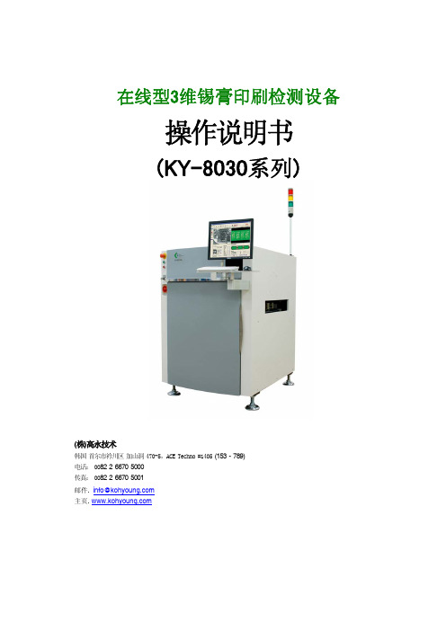
12 | KY-8030 Series
设备运行中的注意事项
危险 设备运行中出现危险状况时,请立刻按下紧急停止(E/STOP、红色)后把电源开关 转到OFF。
紧急停止按钮 (E/Stop)
主电源
危险 由两名以上操作人员运行设备时,请相互提醒避免意想不到的事故。 危险 设备运行过程中不得开启前端安全盖,有可能操作员受伤或损坏设备。 危险 请不要停止安全感应器的工作或变更位置,并需要经常检查感应器状
!
警告
● 小心手受伤 警告 开盖时必须停止设备,避免手受伤。 警告 请不要将手放入盖子里边,避免手受伤。 警告 操作键盘时请不要将手放入盖子里边,避免手受伤。 ● 使用激光 警告 请不要直视激光,避免损伤视力。 警告 设备运行时请不要强行开盖,避免损伤人体或破坏设备。 ● 使用压缩气体 警告 请不要使用气枪清洗或吹干设备零件,避免微笑灰尘损害用户健 康。 警告 请不要将压缩气体喷射到皮肤或眼睛,避免损伤人体。 警告 维修设备时请关闭气压,避免顺伤人体。 ● 处理加热零件 警告 设备运行时,马达零件温度很高。请不要触碰,避免烫伤。
1.1. 1.2. 1.3. 2.1. 2.2. 2.3. 2.4. 2.5.
本体(Main Body) ...................................................................................... 18 操作按钮 ................................................................................................... 19 安全盖传感器 ............................................................................................. 21 设备结构 ................................................................................................... 22 开启电源和开始检测 .................................................................................. 23 关闭设备的顺序 ......................................................................................... 27 软件Bypass模式 ........................................................................................ 28 硬件Bypass模式 ........................................................................................ 29
3A6850H电动泵产品说明书
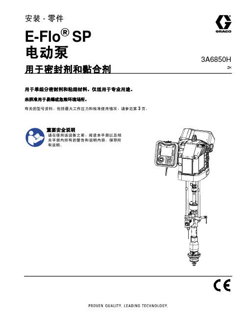
3A6850HZH安装 - 零件E-Flo ®SP 电动泵用于密封剂和黏合剂用于单组分密封剂和粘结材料。
仅适用于专业用途。
未获准用于易爆或危险环境场所。
有关的型号资料,包括最大工作压力和核准使用情况,请参见第 3 页。
重要安全说明请在使用该设备之前,阅读本手册以及相关手册内所有的警告和说明内容。
保存所有说明。
相关手册23A6850H目录相关手册 . . . . . . . . . . . . . . . . . . . . . . . . . . . . . . . . . . 2型号 . . . . . . . . . . . . . . . . . . . . . . . . . . . . . . . . . . . . . . 3系统压力 . . . . . . . . . . . . . . . . . . . . . . . . . . . . . . . 4警告 . . . . . . . . . . . . . . . . . . . . . . . . . . . . . . . . . . . . . . 5部件辨认 . . . . . . . . . . . . . . . . . . . . . . . . . . . . . . . . . . 7带 100 cc Check-Mate CS 下缸体的电动泵 . . . . 7高级显示模块 (ADM) . . . . . . . . . . . . . . . . . . . . . . 8安装 . . . . . . . . . . . . . . . . . . . . . . . . . . . . . . . . . . . . . . 9定位和安装 . . . . . . . . . . . . . . . . . . . . . . . . . . . . . 9接地 . . . . . . . . . . . . . . . . . . . . . . . . . . . . . . . . . . . 9电源要求 . . . . . . . . . . . . . . . . . . . . . . . . . . . . . . . 9连接电源 . . . . . . . . . . . . . . . . . . . . . . . . . . . . . . 10连接独立变压器 . . . . . . . . . . . . . . . . . . . . . . . . . 11在设备使用之前安装开口机油盖 . . . . . . . . . . . . 12流体软管的连接 . . . . . . . . . . . . . . . . . . . . . . . . . 12连接多个泵 . . . . . . . . . . . . . . . . . . . . . . . . . . . . 13设置 . . . . . . . . . . . . . . . . . . . . . . . . . . . . . . . . . . . . . 14湿杯 . . . . . . . . . . . . . . . . . . . . . . . . . . . . . . . . . . 14冲洗泵 . . . . . . . . . . . . . . . . . . . . . . . . . . . . . . . . 14泄压步骤 . . . . . . . . . . . . . . . . . . . . . . . . . . . . . . . . . 16关闭并维护泵 . . . . . . . . . . . . . . . . . . . . . . . . . . . . . . 16驱动器维护 . . . . . . . . . . . . . . . . . . . . . . . . . . . . . . . . 17零配件 . . . . . . . . . . . . . . . . . . . . . . . . . . . . . . . . . . .18带 Check-Mate 下缸体的电动泵 . . . . . . . . . . . .18带 Dura-Flo 下缸体的电动泵 . . . . . . . . . . . . . . .22单向阀 . . . . . . . . . . . . . . . . . . . . . . . . . . . . . . . .25套件及附件 . . . . . . . . . . . . . . . . . . . . . . . . . . . . . . . .28高级显示模块配件包 25E439 . . . . . . . . . . . . . .28通信网关模块 (CGM) 配件包 . . . . . . . . . . . . . . .29入口压力传感器配件包,24Y245 . . . . . . . . . . .30泵架式机架,253692 . . . . . . . . . . . . . . . . . . . .31壁式安装支架,255143 . . . . . . . . . . . . . . . . . .31地板安装适配器,223952 . . . . . . . . . . . . . . . . .32CAN 电缆 . . . . . . . . . . . . . . . . . . . . . . . . . . . . . .32灯塔配件包,255468 . . . . . . . . . . . . . . . . . . . .32I/O 电缆,122029 . . . . . . . . . . . . . . . . . . . . . . .32尺寸 . . . . . . . . . . . . . . . . . . . . . . . . . . . . . . . . . . . . .33E-Flo SP 泵尺寸 . . . . . . . . . . . . . . . . . . . . . . . .33泵机架安装孔图表 . . . . . . . . . . . . . . . . . . . . . . .34地板支脚安装孔图表 . . . . . . . . . . . . . . . . . . . . .35电动驱动器安装孔位置图 . . . . . . . . . . . . . . . . . .35变压器安装孔图表 . . . . . . . . . . . . . . . . . . . . . . .36泵性能 . . . . . . . . . . . . . . . . . . . . . . . . . . . . . . . . . . .37E-Flo SP 性能图表 . . . . . . . . . . . . . . . . . . . . . . .38技术规格 . . . . . . . . . . . . . . . . . . . . . . . . . . . . . . . . . .43美国加州第 65 号提案 . . . . . . . . . . . . . . . . . . . . . . .44Graco 标准保修 . . . . . . . . . . . . . . . . . . . . . . . . . . . .46相关手册这些手册可以从 网站获取。
克罗韦尔CompactLogix5380和Compact GuardLogix5380控制器说明书

CompactLogix 5380 和 Compact GuardLogix 5380 控制器产品目录号 5069-L306ER 、5069-L306ERM 、5069-L310ER 、5069-L310ERM 、5069-L310ER-NSE 、5069-L310ERS2、5069-L320ER 、5069-L320ERM 、5069-L330ER 、5069-L330ERM 、5069-L340ER 、5069-L340ERM 、5069-L350ERM 、5069-L380ERM 、5069-L3100ERM 、5069-L306ERS2、5069-L306ERMS2、5069-L310ERS2、5069-L310ERMS2、5069-L320ERS2、5069-L320ERS2K 、5069-L320ERMS2、5069-L320ERMS2K 、5069-L330ERS2、5069-L330ERS2K 、5069-L330ERMS2、5069-L330ERMS2K 、5069-L340ERS2、5069-L340ERMS2、5069-L350ERS2、5069-L350ERS2K 、5069-L350ERMS2、5069-L350ERMS2K 、5069-L380ERS2、5069-L380ERMS2、5069-L3100ERS2、5069-L3100ERMS2用户手册原版说明书的中文译本重要用户须知在安装、配置、操作或维护本产品前,请仔细阅读本文档以及其他资源部分列出的文档,以了解有关此设备的安装、配置和操作信息。
用户需熟悉所有适用准则、法律及标准要求以及安装和接线说明。
安装、调节、投入使用、操作、装配、拆卸和维护等活动均要求由经过适当培训的人员遵照适用法规执行。
如果未按照制造商指定的方式使用设备,其提供的保护可能会受影响。
对于由于使用或应用此设备而导致的任何间接损失或连带损失,罗克韦尔自动化在任何情况下都不承担任何责任。
TS-538 U, TS-538A U, TS-538B U, TS-538C U 维修手册说明书
REPORTING OF ERRORS
You can improve this manual by recommending improvements using DA Form 2028-2 located in the back of the manual. Ssed form, fill it out as shown on the sample, fold it where shown, and drop it in the mail.
(2) Maintenance code. Maintenance codes are assigned to indicate the levels of maintenance authorized to USE and REPAIR support items. The maintenance codes are entered in the third and fourth positions of the Uniform SMR Code format as follows:
(2) Item number. The number used to identify item called out in the illustration.
b. Source, Maintenance, and Recoverability (SMR) Codes.
(1) Source code. Source codes indicate the manner of acquiring support items for maintenance, repair, or overhaul of end items. Source codes are entered in the first and second positions of the Uniform SMR Code format as follows:
SPS-5380-CXX0G资料
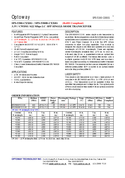
Optoway SPS-5380-CXX0G**********************************************************************************************************************************************************************************************************************************************************************************************************************************************OPTOWAY TECHNOLOGY INC. No .38, Kuang Fu S. Road, Hu Kou, Hsin Chu Industrial Park, Hsin Chu, Taiwan 3031SPS-5380-CXX0G / SPS-5380B-CXX0G (RoHS Compliant)3.3V / CWDM / 622 Mbps LC SFP SINGLE-MODE TRANSCEIVER**********************************************************************************************************************************************************************FEATURESl Hot-Pluggable SFP Footprint LC Optical Transceiver l Small Form-Factor Pluggable (SFP) MSA compatible l 18 Wavelength (λ): 1270 nm to 1610 nm CWDM DFB LD Transmitterl Compliant with SONET OC-12 LR-2 / SDH STM-4 (L-4.2)l 29 dB Power Budget at Leastl AC/AC Coupling according to MSA l Single +3.3 V Power Supply l RoHS Compliantl 0 to 70o C Operation: SPS-5380-CXX0G l -5 to 85o C Operation: SPS-5380B-CXX0Gl Class 1 Laser International Safety Standard IEC-60825 CompliantAPPLICATIONSl ATM Switches and Routersl SONET / SDH Switch Infrastructure l XDSL Applications l Metro Edge SwitchingDESCRIPTIONThe SPS-5380-CXX0G series single mode transceiver is small form factor pluggable module for bi-directional serial optical data communications such as SONET OC-12 / SDH STM-4 and Fiber Channel. It is with the SFP 20-pin connector to allow hot plug capability. This module is designed for single mode fiber and operates at a nominal wavelength of CWDM wavelength. There are eighteen center wavelengths available from 1270 nm to 1610 nm, with each step 20 nm. A guaranteed minimum optical link budget of 29 dB is offered The transmitter section uses a multiple quantum well CWDM DFB laser and is a class 1 laser compliant according to International Safety Standard IEC-60825. The receiver section uses an integrated InGaAs detector preamplifier (IDP) mounted in an optical header and a limiting post-amplifier IC.LASER SAFETYThis single mode transceiver is a Class 1 laser product. It complies with IEC-60825 and FDA 21 CFR 1040.10 and 1040.11. The transceiver must be operated within the specified temperature and voltage limits. The optical ports of the module shall be terminated with an optical connector or with a dust plug.ORDER INFORMATIONP/No.Bit Rate (Mb/s) SONET /SDH Power Budget (dB) Wavelength (nm) PackageTemp. (oC) TX Power (dBm) RX Sens. (dBm) RoHS Compliant SPS-5380-CXX0G 622 LR-2/L-4.2 > 29 CWDM * LC SFP 0 to 70 5 to 0 -29 Yes SPS-5380B-CXX0G622LR-2/L-4.2> 29CWDM *LC SFP-5 to 855 to 0-29YesCWDM * Wavelength (0 to 70o C) Central Wavelength Min. (nm) Typ. (nm)Max. (nm)Central WavelengthMin. (nm)Typ. (nm)Max. (nm)-C270 1264.5 1270 1277.5 -C450 1444.5 1450 1457.5 -C290 1284.5 1290 1297.5 -C470 1464.5 1470 1477.5 -C310 1304.5 1310 1317.5 -C490 1484.5 1490 1497.5 -C330 1324.5 1330 1337.5 -C510 1504.5 1510 1517.5 -C350 1344.5 1350 1357.5 -C530 1524.5 1530 1537.5 -C370 1364.5 1370 1377.5 -C550 1544.5 1550 1557.5 -C390 1384.5 1390 1397.5 -C570 1564.5 1570 1577.5 -C410 1404.5 1410 1417.5 -C590 1584.5 1590 1597.5 -C4301424.514301437.5-C6101604.516101617.5CWDM *: 18 Wavelengths from 1270 nm to 1610 nm, each step 20 nm.******************************************************************************************************************************************************************************OPTOWAY TECHNOLOGY INC. No .38, Kuang Fu S. Road, Hu Kou, Hsin Chu Industrial Park, Hsin Chu, Taiwan 303Absolute Maximum RatingsParameterSymbol Min Max Units NotesStorage TemperatureTstg -40 85 o COperating Case Temperature Topr 0 -5 70 85 o C SPS-5380-CXX0G SPS-5380B-CXX0G Power Supply VoltageVcc-0.53.6VRecommended Operating ConditionsParameterSymbol Min Typ Max Units / NotesPower Supply VoltageVcc 3.1 3.3 3.5 VOperating Case Temperature Topr 0 -5 70 85 oC / SPS-5380-CXX0G oC / SPS-5380B-CXX0GPower Supply Current I CC (TX+RX)200 300 mA Data Rate622Mb/sTransmitter Specifications (0o C < Topr < 70o C, 3.1V < Vcc < 3.5V)ParameterSymbolMinTypMaxUnitsNotesOpticalOptical Transmit Power Po 0 --- 5 dBm 1Output Center Wavelength λλc –5.5 λc λc +7.5 nm 2 Output Spectrum Width ∆λ --- --- 1 nm -20 dB Width Side Mode Suppression Ratio SMSR 30 dB Extinction Ratio E R 10 --- --- dB Output Eye Compliant with Bellcore TR-NWT-000253 and ITU recommendation G.957 Optical Rise Time t r 1.2 ns 10 % to 90% Values Optical Fall Time t f 1.2 ns 10 % to 90% Values Relative Intensity Noise RIN -120 dB/Hz ElectricalData Input Current – Low I IL -350 µA Data Input Current – High I IH 350 µA Differential Input Voltage V IH - V IL 0.5 2.4 V Peak-to-Peak TX Disable Input Voltage – Low T DIS, L 0 0.5 V 3 TX Disable Input Voltage – High T DIS, H 2.0 Vcc V 3 TX Disable Assert Time T ASSERT 10 µsTX Disable Deassert Time T DEASSERT 1 msTX Fault Output Voltage -- Low T FaultL 0 0.8 V 4 TX Fault Output Voltage -- High T FaultH 2.0 Vcc+0.3 V 4 1. Output power is power coupled into a 9/125 µm single mode fiber.2. ITU-T G.694.2 CWDM wavelength from 1270 nm to 1610 nm, each step 20 nm.3. There is an internal4.7K to 10K ohm pull-up resistor to VccTX.4. Open collector compatible, 4.7K to 10K ohm pull-up to Vcc (Host Supply Voltage).Receiver Specifications (0o C < Topr < 70o C, 3.1V < Vcc < 3.5V)ParameterSymbol Min Typ Max Units NotesOptical SensitivitySens -29 dBm 4 Maximum Input Power Pin -8 dBm 4Signal Detect -- Asserted Pa --- -29 dBm Transition: low to high Signal Detect -- Deasserted Pd -40 --- --- dBm Transition: high to low Signal detect -- Hysteresis 1.0 --- dBWavelength of Operation1100---1620nm******************************************************************************************************************************************************************************OPTOWAY TECHNOLOGY INC. No .38, Kuang Fu S. Road, Hu Kou, Hsin Chu Industrial Park, Hsin Chu, Taiwan 303ElectricalDifferential Output Voltage V OH – V OL 0.6 2.0 V Output LOS Voltage -- Low V OL 0 0.8 V 5 Output LOS Voltage -- HighV OH2.0Vcc+0.3V54. Measured at 223-1 PRBS at BER 1E-10.5. Open collector compatible, 4.7K to 10K ohm pull-up to Vcc (Host Supply Voltage).Module DefinitionModule DefinitionMOD-DEF2 PIN 4 MOD-DEF1 PIN 5 MOD-DEF0 PIN 6 Interpretation by Host 4SDASCLLV-TTL LowSerial module definitionprotocolModule Definition 4 specifies a serial definition protocol. For this definition, upon power up, MOD-DEF(1:2) appear as no connector (NC) and MOD-DEF(0) is TTL LOW. When the host system detects this condition, it activates the serial protocol. The protocol uses the 2-wire serial CMOS E 2PROM protocol of the ATMEL AT24C01A/02/04 family of components.****************************************************************************************************************************************************************************** OPTOWAY TECHNOLOGY INC. No.38, Kuang Fu S. Road, Hu Kou, Hsin Chu Industrial Park, Hsin Chu, Taiwan 303。
HM538123BJ-8资料
SAM Column Decoder
Column Decoder
Transfer Gate
Data Register
0 255 Memory Arra交易网
HM538123B Series
Pin Functions
5$6 (input pin):
Features
• Multiport organization Asynchronous and simultaneous operation of RAM and SAM capability RAM: 128-kword × 8-bit and SAM: 256-word × 8-bit • Access time RAM: 60 ns/70 ns/80 ns/100 ns max SAM: 20 ns/22 ns/25 ns/25 ns max • Cycle time RAM: 125 ns/135 ns/150 ns/180 ns min SAM: 25 ns/25 ns/30 ns/30 ns min • Low power Active RAM: 413 mW max SAM: 275 mW max Standby 38.5 mW max • High-speed page mode capability • Mask write mode capability • Bidirectional data transfer cycle between RAM and SAM capability • Split transfer cycle capability • Block write mode capability • Flash write mode capability
Note: X; Don’t care
危险化学品特性表
危险化学品特性表(自制)危险化学品特性表(自制) (1)(1)丙烯酸 (3)(2)甲酸 (4)(3)氢氟酸 (6)(1)N,N—二甲基甲酰胺 (7)(2)丙烯酸丁酯 (8)(1)萘 (10)(2)乌洛托品 (11)(1)氯酸钠 (13)(2)亚硝酸钠 (14)(1)四氯乙烯 (15)3。
1。
1。
1丙酮 (18)3.1。
1.2-丁酮 (20)3.1。
1。
3甲醇 (21)3.1。
1.4乙醇 (22)3.1。
1。
5 环己酮 (24)3。
1.1.6异丙醇 (25)3。
1.1.7 甲苯 (27)3.1。
1.8 1,2—二甲苯 (29)3.1.1。
9 乙醚 (30)3。
1。
1。
10 乙酸乙酯 (32)3.1。
1.11过氧化氢 (33)3.1。
1.12高锰酸钾 (35)3.1.1。
13重铬酸钾 (36)3。
1.1。
14硝酸银 (38)3。
1。
1.15苯酚 (39)3.1。
1。
16三氯甲烷 (41)3.1.1.17四氯化碳 (42)3.1.1。
18氢氧化铵水溶液 (44)3。
1。
1。
19氢氧化钠 (45)3.1。
1。
20氢氧化钾 (46)3。
1.1。
21甲醛 (47)3。
1.1.22盐酸 (49)3。
1.1。
23硝酸 (51)3.1。
1。
24硫酸 (52)3。
1。
1。
25 乙酸 (54)3。
1。
1。
26三氯乙酸 (56)3.1。
1.27氢氟酸 (57)3.1.1。
28次氯酸钠 (59)3.1.1。
29亚硫酸氢钠 (60)(4)纯苯 (62)(5)1,1—二氯乙烷 (63)(7)正丁醇 (65)(10)二(正)丁醚 (66)(11)丙烯酸正丁酯 (68)(4)冰醋酸 (69)三氯乙醛 (70)硝酸钠 (72)连二亚硫酸钠 (73)石油醚 (74)对二甲苯 (76)氧 (77)乙炔 (78)⑺乙酸酐 (80)(1)丙烯酸表3.1-1 丙烯酸简介(2)甲酸表3。
1-2甲酸简介(3)氢氟酸表3。
1-3氢氟酸简介(1)N,N—二甲基甲酰胺表3.1—4 N,N—二甲基甲酰胺简介(2)丙烯酸丁酯表3.1-5丙烯酸丁酯简介(1)萘表3。
- 1、下载文档前请自行甄别文档内容的完整性,平台不提供额外的编辑、内容补充、找答案等附加服务。
- 2、"仅部分预览"的文档,不可在线预览部分如存在完整性等问题,可反馈申请退款(可完整预览的文档不适用该条件!)。
- 3、如文档侵犯您的权益,请联系客服反馈,我们会尽快为您处理(人工客服工作时间:9:00-18:30)。
5 mm (T13/4) LED, Diffused Wide-Angle LED
LS 5380, LY 5380, LG 5380
Streuung der Lichtstärke in einer Verpackungseinheit I V max /I V min ≤ 2.0.Luminous intensity ratio in one packaging unit I V max /I V min ≤ 2.0.
Typ Type
Emissionsfarbe Color of Emission
Gehäusefarbe Color of Package
Lichtstärke Luminous Intensity I F = 10 mA I V (mcd)Bestellnummer Ordering Code
LS 5380-FJ LS 5380-G LS 5380-H LS 5380-J LS 5380-HL super-red red diffused
1.0…8.01.6… 3.2
2.5… 5.04.0…8.02.5… 20.0Q62703-Q1452Q62703-Q1740Q62703-Q1453Q62703-Q1454Q62703-Q1455LY 5380-GK LY 5380-H LY 5380-J LY 5380-K LY 5380-HL yellow yellow diffused
1.6… 1
2.52.5… 5.04.0…8.06.3… 12.52.5… 20.0Q62703-Q2002Q62703-Q1457Q62703-Q2319Q62703-Q3909Q62703-Q2003LG 5380-GK LG 5380-H LG 5380-J LG 5380-K LG 5380-HL
green green diffused
1.6… 1
2.52.5… 5.04.0…8.06.3… 12.52.5
… 20.0
Q62703-Q1463Q62703-Q2032Q62703-Q2016Q62703-Q3189Q62703-Q3825
V E X 06715
Besondere Merkmale
q eingefärbtes, diffuses “Low Profile”-Gehäuse q als optischer Indikator einsetzbar q Lötspieße ohne Aufsetzebene q gegurtet lieferbar
q
Störimpulsfest nach DIN 40839
Features
q colored, diffused “Low Profile”-package q for use as optical indicator q solder leads without stand-off q available taped on reel
q
load dump resistant acc. to DIN 40839
Grenzwerte Maximum Ratings
Bezeichnung Parameter Symbol
Symbol
Werte
Values
Einheit
Unit
Betriebstemperatur Operating temperature range T
op
– 55 … + 100˚C
Lagertemperatur
Storage temperature range T
stg
– 55 … + 100˚C
Sperrschichttemperatur Junction temperature T
j
+ 100˚C
Durchlaßstrom Forward current I
F
40mA
Stoßstrom
Surge current
t≤ 10µs, D = 0.005I
FM
0.5A
Sperrspannung Reverse voltage V
R
5V
Verlustleistung Power dissipation
T A ≤ 25˚C
P
tot
140mW
Wärmewiderstand Thermal resistance Sperrschicht / Luft Junction / air R
th JA
400K/W
Kennwerte (T A = 25˚C)Characteristics Bezeichnung Parameter
Symbol Symbol
Werte Values Einheit Unit
LS
LY LG Wellenlänge des emittierten Lichtes (typ.)Wavelength at peak emission (typ.)I F = 20 mA
λpeak 635
586
565
nm Dominantwellenlänge (typ.)Dominant wavelength (typ.)
I F = 20 mA
λdom 628590570nm
Spektrale Bandbreite bei 50 %I rel max (typ.)Spectral bandwidth at 50 %I rel max (typ.)I F = 20 mA
∆λ454525nm
Abstrahlwinkel bei 50 %I V (Vollwinkel)Viewing angle at 50 %I V 2ϕ
140140140Grad deg.Durchlaßspannung (typ.)Forward voltage (max.)I F = 10 mA V F V F 2.02.6 2.02.6 2.02.6V V Sperrstrom
(typ.)Reverse current (max.)V R = 5 V
I R I R 0.01100.01100.0110µA µA Kapazität (typ.)Capacitance
V R = 0 V, ƒ = 1 MHz
C 0
12
10
15
pF
Schaltzeiten:Switching times:
I V from 10 % to 90 %(typ.)I V from 90 % to 10 %
(typ.)I F = 100 mA,t P = 10µs,R L = 50Ω
t r t f
300150300150450200ns ns
Relative spektrale Emission I rel=f(λ),T A= 25˚C,I F= 20mA Relative spectral emission
V (λ) =spektrale Augenempfindlichkeit
Standard eye response curve
Abstrahlcharakteristik I rel=f(ϕ)
Radiation characteristic
Durchlaßstrom I F =f (V F )Forward current T A
= 25˚C Zulässige Impulsbelastbarkeit I F =f (t P )Permissible pulse handling capability Duty cycle D = parameter,T A = 25
˚C Relative Lichtstärke I V /I V(10mA) =f (I F )Relative luminous intensity T A = 25˚C
Maximal zulässiger Durchlaßstrom Max. permissible forward current I F =f (T A
)
Wellenlänge der Strahlung λpeak =f (T A )Wavelength at peak emission I
F = 20mA
Durchlaßspannung V F =f (T A )Forward voltage I F = 10
mA Dominantwellenlänge λdom =f (T A )Dominant wavelength
I
F = 20mA
Relative Lichtstärke
I V /I V(25°C) =f (T A )Relative luminous intensity I F = 10
mA
Maßzeichnung(Maße in mm, wenn nicht anders angegeben) Package Outlines(Dimensions in mm, unless otherwise specified)
Kathodenkennzeichnung:Kürzerer LötspießCathode mark:Short solder lead G E X 0 6 7 1 5。