5082-K121-GD000中文资料
东莞龙海化工有限公司产品单面资料

251 耐磨手感蜡 浆
252 不消光耐磨 蜡浆
252A 不消光手感 蜡浆
1.由于较高的堆积密度,所以常用来消 外观:白色微粒粉末 光。 高分子聚合物 平均粒径(Micron): 2.应用于高档UV涂料,UV地板漆,烤漆 2-3 光油,家私漆、装修漆、一般的工业涂 外观:浅黄色微粒粉 末 改性巴西棕榈蜡 不消光、保光、印铁、皮革涂层中 平均粒径(Micron): 6~9 外观 :白色微粒粉 1.具有优良的透明度和爽滑的手感。 末 PTFE 平均粒径(Micron): 2.应用于高档家私漆、装修漆、一般的 工业涂料,卷钢涂料,粉末涂料中增加 6~8 外观 :白色微粒粉 1.高耐RCA性能 2.236由于粒径小且均匀,用在银粉漆中 末 PTFE 平均粒径(Micron): 抗刮伤好,还不会影响铝粉的定向排列 。用在不粘锅涂料中效果也非常好 3~4 1.最大粒径不超2微米,粒径分布非常均 外观:白色微粒粉末 PTFE改性高分子聚 匀 。 平均粒径(Micron): 合体 2.粒径小且均匀,所以对涂层基本不消 1~2 光,克服了其它蜡的缺点,但应高速分散 外 观:白色胶状 有效份:18% 1.具有非常好的手感和抗刮性,也有很 氟改性蜡浆 溶 剂:XYL/BAC 佳的透明性,不影响流平和光泽; 熔 点:140 2.广泛推荐用于涂料、油墨中 外 观:白色胶状 1.粒度小,不会影响光泽; 2.主要应用于一些对光泽要求高而且对 有效份:30% 氟改性蜡浆 耐磨也有相当要求的体系中, 粒径:小于7微米 3.印铁、工业烤漆、塑胶漆。 溶 剂:二甲苯 外 观:白色胶状 1.粒度小,不会影响光泽;帮助流平, 手感滑爽 有效份:26% 改性蜡浆 粒径:小于7微米 2.主要应用于一些对光泽要求高而且对 耐磨也有相当要求的体系中, 溶 剂:二甲苯
广州荣士电子公司 水控机 说明书
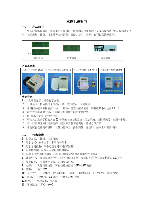
水控机说明书一、 产品产品简介简介中文液显水控机是广州荣士电子公司自主研发的国内独家的中文液晶显示水控机。
显示功能齐全:包括余额、计费、用水量等实时信息,简洁、易用、合理,有利提高管理效率。
<-->待机画面消费画面提示画面产品系列产品系列表表中文一体计量型SK071中文分体计量型SK072中文分体计时型SK073中文开水计时型SK075功能特点1、中文液晶显示,操作提示齐全。
2、一机多卡,按流量(升)/时间计费,放卡取水,卡离断水。
3、计时控水模式下精确到1秒,计量控水模式下按照流量计的精度最小可达到0.01升。
4、阶梯式价格计费方式,不同累计用量按不同的价格收费。
5、防“滴水不走表”的偷水行为6、可接入企业或学校的其它IC 卡系统(如考勤系统、门禁系统、售饭系统等)实现一卡通。
7、有一体机和分体机可供选择,按实际安装环境实行一体或分体安装。
8、系统配套设备简单易用,软件功能齐全,操作简便,免培训,基本上不需要维护。
二、 技术参数1、收费方式: 计时、计量可选2、用水方式:放卡出水,卡离自动关水3、用水时间控制:四个可设时用水时间的间段4、用水量控制:可按每天或每月限量用水5、电磁阀直接电压控制模式 或 电磁阀防驳接偷水的加密控制模式。
6、计量单位: 金额以分为单位,时间以秒为单位,流量以升为单位(流量精度为0.01升)7、费率设置: 阶梯费率扣费,先扣费后出水。
8、电源: 内置稳压电路,可自动适应直流 12V—24V 电源 9、功率: 小于2W10、尺寸大小: 分体机:155×90×38,一体机:135×90×108 (长*宽*高,单位mm ) 11、重量: 分体机:0.2公斤,一体机:0.5公斤 12防水: 密封胶条、密封胶 13、环境温度: 0ºC —60ºC14、环境湿度: 随意三、 安装安装水控机水控机水控机说明说明1、 安装安装示意图示意图2、 安装注意事项A 、 水流方向。
5082-2800中文资料

Schottky Barrier Diodes for General Purpose ApplicationsTechnical DataFeatures• Low Turn-On VoltageAs Low as 0.34 V at 1 mA• Pico Second Switching Speed • High Breakdown VoltageUp to 70 V• Matched Characteristics AvailableDescription/Applications The 1N5711, 1N5712, 5082-2800/ 10/11 are passivated Schottky barrier diodes which use a patented “guard ring” design to achieve a high breakdown voltage. Packaged in a low cost glass package, they are well suited for high level detecting, mixing, switching, gating, log or A-D converting, video detecting, frequency discriminating, sampling, and wave shaping.The 5082-2835 is a passivatedSchottky diode in a low cost glasspackage. It is optimized for lowturn-on voltage. The 5082-2835 isparticularly well suited for theUHF mixing needs of the CATVmarketplace.The 5082-2300 Series and5082-2900 devices are unpas-sivated Schottky diodes in a glasspackage. These diodes haveextremely low 1/f noise and areideal for low noise mixing, andhigh sensitivity detecting. Theyare particularly well suited for usein Doppler or narrow band videoreceivers.1N57111N57125082-2300 Series5082-2800 Series5082-2900DIMENSIONS IN MILLIMETERS AND (INCHES).Outline 15Maximum RatingsJunction Operating and Storage Temperature Range5082-2303, -2900.................................................................-60°C to +100°C 1N5711, 1N5712, 5082-2800/10/11....................................-65°C to +200°C 5082-2835............................................................................-60°C to +150°C DC Power Dissipation(Measured in an infinite heat sink at T CASE = 25°C)Derate linearly to zero at maximum rated temperature5082-2303, -2900..............................................................................100 mW 1N5711, 1N5712, 5082-2800/10/11.................................................250 mW 5082-2835.........................................................................................150 mW Peak Inverse Voltage.................................................................................V BRPackage CharacteristicsOutline 15Lead Material........................................................................................DumetLead Finish..............................................................................95-5% Tin-LeadMax. Soldering Temperature................................................260°C for 5 secMin. Lead Strength....................................................................4 pounds pullTypical Package Inductance1N5711, 1N5712:................................................................................2.0 nH2800 Series:........................................................................................2.0 nH2300 Series, 2900:..............................................................................3.0 nHTypical Package Capacitance1N5711, 1N5712:................................................................................0.2 pF2800 Series:........................................................................................0.2 pF2300 Series, 2900:............................................................................0.07 pFThe leads on the Outline 15 package should be restricted so that thebend starts at least 1/16 inch from the glass body.Outline 15 diodes are available on tape and reel. The tape and reelspecification is patterned after RS-296-D.Electrical Specifications at T= 25°CAGeneral Purpose DiodesMin.Max.V F = 1 V Max.Max.Max.Breakdown Forward at Forward Reverse Leakage Capaci-Part Package Voltage Voltage Current Current tance Number Outline V BR (V)V F (mV)I F (mA)I R (nA) at V R (V)C T (pF) 5082-280015704101520050 2.0 1N571115704101520050 2.0 5082-281015204103510015 1.2 1N571215205503515016 1.2 5082-28111515410201008 1.2 5082-2835158*34010*1001 1.0 Test I R = 10 µA I F = 1 mA*V F = 0.45 V V R = 0 V Conditions*I R = 100 µA f =1.0 MHz Note: Effective Carrier Lifetime (τ) for all these diodes is 100 ps maximum measured with Krakauer method at 5 mA except for 5082-2835 which is measured at 20 mA.Low 1/f (Flicker) Noise DiodesMin.Max.V F = 1 V Max.Max.Max.Part Breakdown Forward at Forward Reverse Leakage Capaci-Number Package Voltage Voltage Current Current tance 5082-Outline V BR (V)V F (mV)I F (mA)I R (nA) at V R (V)C T (pF) 230315204003550015 1.0 29001510400201005 1.2 Test I R = 10 µA I F = 1 mA V R = 0 V Conditions f =1.0 MHzNote: Effective Carrier Lifetime (τ) for all these diodes is 100 ps maximum measured with Krakauer method at 20 mA.Matched Pairs and QuadsBasic Matched MatchedPart Number Pair Quad Batch5082-Unconnected Unconnected Matched[1]Test Conditions2900∆VF at IF= 1.0, 10 mA28005082-28045082-2805∆V F at I F = 0.5, 5 mA ∆V F = 20 mV∆V F = 20 mV*I F = 10 mA∆C O at f = 1.0 MHz28115082-2826∆VF at IF= 10 mA∆V F = 10 mV∆C O at f = 1.0 MHz ∆C O = 0.1 pF28355082-2080∆VF at IF=10 mA∆V F = 10 mV∆C O at f = 1.0 MHz∆C O = 0.1 pFNote:1. Batch matched devices have a minimum batch size of 50 devices.SPICE ParametersParameter Units5082-28005082-28105082-28115082-28355082-23035082-2900B V V75251892510C J0pF 1.60.8 1.00.70.7 1.1E G eV0.690.690.690.690.690.69I BV A10E-510E-510E-510E-510E-510E-5I S A 2.2 x 10E-9 1.1 x 10E-90.3 x 10E-8 2.2 x 10E-87 x 1.0E-910E-8N 1.08 1.08 1.08 1.08 1.08 1.08 R SΩ25101051015 P B V0.60.60.60.560.640.64 PT222222 M0.50.50.50.50.50.5Typical ParametersV F – FORWARD VOLTAGE (V)Figure 1. I-V Curve Showing Typical Temperature Variation for 5082-2300 Series and 5082-2900 Schottky Diodes.1001010.10.01I F - F O R W A R D C U R R E N T (m A )V BR (V)Figure 2. 5082-2300 Series Typical Reverse Current vs. Reverse Voltage at Various Temperatures.10.0001,000100101I R (n A )051015100755025T A = 25°CI F - FORWARD CURRENT (mA)Figure 3. 5082-2300 Series and 5082-2900 Typical Dynamic Resistance (R D ) vs. Forward Current (I F ).100010010R D - D Y N A M I C R E S I S T AN C E (Ω)0.01010100V R - REVERSE VOLTAGE (V)Figure 4. 5082-2300 and 5082-2900 Typical Capacitance vs. Reverse Voltage.1.21.00.80.60.40.20C T - C A P A C I T A N C E (p F )048121620V F - FORWARD VOLTAGE (V)Figure 5. I-V Curve Showing Typical Temperature Variation for 5082-2800 or 1N5711 Schottky Diodes.5010510.50.10.050.01I F - F O R W A R D C U R R E N T (m A )00.20.40.60.8 1.0 1.2V R - REVERSE VOLTAGE (V)Figure 6. (5082-2800 OR 1N5711) Typical Variation of Reverse Current (I R ) vs. Reverse Voltage (V R ) at Various Temperatures.100,00010,0001000100101I R - R E V E R S E C U R R E N T (n A )0.20.40.60.81.01.2V R - REVERSE VOLTAGE (V)Figure 7. (5082-2800 or 1N5711)Typical Capacitance (C T ) vs. Reverse Voltage (V R ).12.01.51.00.50C T - C A P A C I T A N C E (p F )010********V F - FORWARD VOLTAGE (V)Figure 8. I-V Curve Showing Typical Temperature Variation for the 5082-2810 or 1N5712 Schottky Diode.100101.00.10.01I F - F O R W A R D C U R R E N T (m A )V R - REVERSE VOLTAGE (V)Figure 9. (5082-2810 or IN5712)Typical Variation of Reverse Current (I R ) vs. Reverse Voltage (V R ) at Various Temperatures.10,0001000100101.0I R - R E V E R S E C U R R E N T (n A )Typical Parameters, continuedV F - FORWARD VOLTAGE (V)Figure 10. I-V Curve Showing Typical Temperature Variation for the 5082-2811 Schottky Diode.100101.00.10.01I F - F O R W A R D C U R R E N T (m A )0.40.20.60.81.01.2V R - REVERSE VOLTAGE (V)Figure 11. (5082-2811) Typical Variation of Reverse Current (I R ) vs. Reverse Voltage (V R ) at Various Temperatures.100,00010,0001000100101I R - R E V E R S E C U R R E N T (n A )0510********V F - FORWARD VOLTAGE (V)Figure 12. I-V Curve Showing Typical Temperature Variations for 5082-2835 Schottky Diode.100101.00.10.01I F - F O R W A R D C U R R E N T (m A )00.20.40.60.8 1.0 1.2V R - REVERSE VOLTAGE (V)Figure 13. (5082-2835) Typical Variation of Reverse Current (I R ) vs. Reverse Voltage (V R ) at Various Temperatures.100,00010,0001000100101I R - R E V E R S E C U R R E N T (n A )0123456V R - REVERSE VOLTAGE (V)Figure 14. Typical Capacitance (C T ) vs. Reverse Voltage (V R ).C T - C A P A C I T A N C E (p F )0246810I F - FORWARD CURRENT (mA)Figure 15. Typical Dynamic Resistance (R D ) vs. Forward Current (I F ).1000100101R D - D Y N A M I C R E S I S T A N C E (Ω)Diode Package Marking1N5xxx5082-xxxxwould be marked:1Nx xxxxx xxYWW YWWwhere xxxx are the last four digits of the 1Nxxxx or the 5082-xxxx partnumber. Y is the last digit of the calendar year. WW is the work week ofmanufacture.Examples of diodes manufactured during workweek45 of 1999:1N57125082-3080would be marked:1N53071280945945Data subject to change.Copyright © 1999 Agilent TechnologiesObsoletes 5968-4304E5968-7181E (11/99)。
GD2000-异径管
(2000 版)
第三章
异径管
异径管索引
序号 标识编码
钢管模压异径管
1
R4.2A12SO
2
R5.3A12SO
3
R9.81A13SO
4
R9.81A21SO
5
R13.73A13SO
6
R13.73A21SO
7
R17.6A13SO
8
R25.4A13SO
索引
压力 MPa
温度 ℃
普通 普通 普通 普通 普通 普通 普通 普通 普通
钢板焊制偏心异径管 普通 钢板焊制偏心异径管 普通
异径管索引
序号 标识编码
3
R1.6C11WE
4
R1.6A11WE
5
R1.6S11WE
6
R1.0C12WE
7
R1.0C11WE
8
R1.0A11WE
9
R1.0S11WE
压力 MPa
温度 ℃
材料
PN1.6
- 99 -
钢管模压异径管 钢管模压异径管 钢管模压异径管 钢管模压异径管 钢管模压异径管 钢管模压异径管 钢管模压异径管 钢管模压异径管 钢管模压异径管 钢管模压异径管 钢管模压异径管
高压给水 高压给水 高压给水 高压给水 高压给水(关断阀前) 高压给水(关断阀前) 高压给水(关断阀前) 高压给水(关断阀后) 高压给水(关断阀后) 高压给水(关断阀后) 高压给水(关断阀前)
17.15 230
17.15 230
22.56 257
22.56 257
27.3 185
27.3 185
27.3 185
24.6 285
宝钢热镀锌产品相近牌号对照表

-
SS 550
H220PD+Z,H220PD+ZF
H220PD+Z,+ZF
-
-
-
H260PD+Z,H260PD+ZF
H260PD+Z,+ZF
-
-
-
H300LAD+Z,H300LAD+ZF
H300LAD+Z,+ZF
-
-
-
H340LAD+Z(HSA340Z), H340LAD+ZF
H180YD+Z,+ZF
-
-
-
H220YD+Z,H220YD+ZF
H220YD+Z,+ZF
-
-
-
H260YD+Z,H260YD+ZF
H260YD+Z,+ZF
-
-
-
H180BD+Z,H180BD+ZF
H180BD+Z,+ZF
-
-
-
H220BD+Z,H220BD+ZF
H220BD+Z,+ZF
-
-
-
H260BD+Z,H260BD+ZF
SGC340
SS 275
S320GD+Z,S320GD+ZF
S320GD+Z,+ZF
FeE320GZ, ZF
-
-
S350GD+Z(StE345-2Z) S350GD+ZF
S350GD+Z,+ZF
MP-508土壤水分测定仪打印版说明书解析

MP-508型土壤水分速测仪使用说明书邯郸市锐研智华电子科技有限公司目录1.仪器简介2.仪器主要技术特性3.仪器的使用4.键盘5.显示屏6.软件安装和数据下载7.仪器的保养8.应用范围和技术1.仪器简介1-1.仪器的组成部分l-l-1.水分探测器(传感器MP-508B 工作原理MP-508B 由一个内含电子器件的防水室和与之一端相连的四个不锈钢针的成形的探针组成。
这些探针直接插入土壤。
探头尾部的电缆线连接适宜的电压源和输出模拟信号。
它是一种模拟设备,不断产生电信号和以电压比表示土壤性质。
MP-508B 通过特殊设计的传输线产生高频信号,测量土壤参数。
该传输线的阻抗随土壤阻抗变化而变化。
阻抗包括表观介电常数和离子传导率。
选用电信号的频率使离子传导率的影响最小,以使传输线阻抗变化几乎仅依赖于土壤介电常数的变化。
这些变化产生一个电压驻波。
驻波随探针周围介质的变化增加或减小晶体振荡器产生的电压。
MP-508B 利用振荡器产生的电压和探针返回电压的差值测量土壤的介电常数。
因为仅在制造过程中调节探头以产生一个与已知介电常数对应的一致的输出电压.所以每个508B 无需系统标定即可互换使用。
Whalley,White,Knight,Zegelin,Topp 等人多年来的工作表明了介电常数的平方根与土壤容积含水量存在线性关系,且这种关系适宜于多种土壤。
输出电压在0-lVDC 表示土壤介电常数在1-32之间。
这一范围代表一般矿质土壤的体积含水量50%。
电子和机械参数:1-1-2.手持仪表该手持仪表专为湿度探测器MP-508配合使用。
该仪器采用微电脑芯片进行控制,运算,存储。
采用了12位精度的AD 变换器,使测量显示精度提高,并由一个16位液晶显示器显示测量结果,在对土壤进行水分测量时,仪表可以直接显示体积含水量。
由于湿度探测器是采用高频技术对被测介质的相对介电常数Ka 进行测量,为了使仪器能够对不同类型的土壤以及其它微粒或粉末甚至液体物质进行水分测量,仪表在显示土壤水分含量的同时,显示毫伏值,扩大了仪器的使用范围。
陕西科技大学过程设备制造与检测课程设计说明书模板

目录一,制造背景 (2)1.2设计参数 (2)1。
3技术要求 (3)1。
4储气罐的结构分析 (4)1.4.1筒体结构分析 (4)二,筒体材料 (5)三.筒体具体制造工艺 (5)1。
材料的进厂入库检测 (5)2. 放样,划线与号料 (7)2.1筒节下料 (8)3,简体的卷制成形 (9)4,筒节坡口加工与焊接 (10)4,1。
1简体纵焊缝坡口加工 (10)4,1。
2简体环焊缝坡口 (11)4,1.3 焊接 (11)5,校圆 (12)6,检测 (14)7,组对 (14)8,焊接 (15)9,检测 (16)四,心的体会 (16)一,制造背景1.1液化石油气,英文名称: Liquefied petroleum ges,主要成分:乙烯、乙烷、丙烷、丙烯、丁烷、丁烯等.随着石油化学工业的发展,液化石油气作为一种化工基本原料和新型燃料,已愈来愈受到人们的重视。
在化工生产方面,液化石油气经过分离得到乙烯、丙烯、丁烯、丁二烯等,用来生产合塑料、合成橡胶、合成纤维及生产医药、炸药、染料等产品.用液化石油气作燃料,由于其热值高、无烟尘、无炭渣,操作使用方便,已广泛地进入人们的生活领域。
此外,液化石油气还用于切割金属,用于农产品的烘烤和工业窑炉的焙烧等。
而液化石油气储罐是具有较大危险性的储存容器,一旦出现问题,将给人民的生命、财产带来极大的损失。
吉林、西安等地的液化气储罐事故给人们以深刻的教训。
为了保证液化石油气储罐的安全运行,避免事故发生,必须从个方面严格把关,其中,筒节的制作过程是关键中的关键。
产品名称: 40M3液化石油气卧式储罐产品类别:三按照《特种设备安全监察条例》的规定,该台产品经制造单位监督检验,安全性能符合《压力容器安全基数监察规程》,《GB150-1998 钢制压力容器标准》及设计图样的规定。
1。
2设计参数1。
3技术要求(1)本设备按照GB150—1998《钢制压力容器》进行制造,检测与验收,并接受《压力容器安全技术监察规程》的监督。
米顿罗计量泵系列全系列产品电子样本
A1 22 L/hr 17.3 BarG
A146 ---- 350TI
Acrylic PE 0.25 O.D.
B
4-20mA
B1 B7 B9
(0-26.5 L/hr, 0-10.3 BarG)
Y
Acrylic
PVC
PVDF
316SS
B116-Y B716-Y B916-Y
490TI
398TI
392TI
0.25 NPTM 0.25 NPTM 0.5 NPTM 0.25 NPTM 0.25 NPTM 0.5 NPTM PE 0.5 PE 0.5 0.25 NPTM 0.5 PE 0.5 PE 0.5 0.5 0.5 0.5 0.5 PE 0.5 PE 0.375 PE 0.375 PE 0.375 PE 0.375 PE 0.375 0.25 NPTM
297
0.046
6.1
B126-Y B726-Y B926-Y
490TI
398TI
392TI
297
0.048
9.5
B136-Y B736-Y B936-Y
460TI
368TI
HDSP-N40X资料
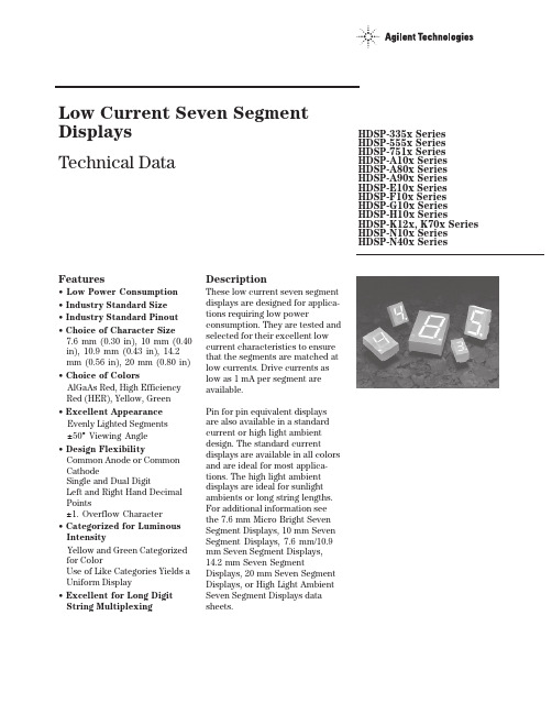
Features• Low Power Consumption • Industry Standard Size• Industry Standard Pinout • Choice of Character Size7.6 mm (0.30 in), 10 mm (0.40 in), 10.9 mm (0.43 in), 14.2 mm (0.56 in), 20 mm (0.80 in)• Choice of ColorsAlGaAs Red, High Efficiency Red (HER), Yellow, Green• Excellent Appearance Evenly Lighted Segments±50° Viewing Angle• Design FlexibilityCommon Anode or Common CathodeSingle and Dual DigitLeft and Right Hand Decimal Points±1. Overflow Character• Categorized for Luminous IntensityYellow and Green Categorized for ColorUse of Like Categories Yields a Uniform Display• Excellent for Long Digit String Multiplexing DescriptionThese low current seven segment displays are designed for applica-tions requiring low power consumption. They are tested and selected for their excellent low current characteristics to ensure that the segments are matched at low currents. Drive currents as low as 1 mA per segment are available.Pin for pin equivalent displays are also available in a standard current or high light ambient design. The standard current displays are available in all colors and are ideal for most applica-tions. The high light ambient displays are ideal for sunlight ambients or long string lengths. For additional information see the 7.6 mm Micro Bright Seven Segment Displays, 10 mm Seven Segment Displays, 7.6 mm/10.9 mm Seven Segment Displays, 14.2 mm Seven Segment Displays, 20 mm Seven Segment Displays, or High Light Ambient Seven Segment Displays data sheets.Low Current Seven SegmentDisplays Technical Data HDSP-335x SeriesHDSP-555x SeriesHDSP-751x SeriesHDSP-A10x Series HDSP-A80x Series HDSP-A90x Series HDSP-E10x Series HDSP-F10x Series HDSP-G10x Series HDSP-H10x Series HDSP-K12x, K70x Series HDSP-N10x SeriesHDSP-N40x SeriesDevicesAlGaAs HER Yellow Green Package HDSP-HDSP-HDSP-HDSP-Description Drawing A1017511A801A9017.6 mm Common Anode Right Hand Decimal A A1037513A803A9037.6 mm Common Cathode Right Hand Decimal B A1077517A807A9077.6 mm Common Anode ±1. Overflow C A1087518A808A9087.6 mm Common Cathode ±1. Overflow D F10110 mm Common Anode Right Hand Decimal E F10310 mm Common Cathode Right Hand Decimal F F10710 mm Common Anode ±1. Overflow G F10810 mm Common Cathode ±1. Overflow H G10110 mm Two Digit Common Anode Right Hand Decimal X G10310 mm Two Digit Common Cathode Right Hand Decimal Y E100335010.9 mm Common Anode Left Hand Decimal I E101335110.9 mm Common Anode Right Hand Decimal J E103335310.9 mm Common Cathode Right Hand Decimal K E106335610.9 mm Universal ±1. Overflow[1]L H101555114.2 mm Common Anode Right Hand Decimal M H103555314.2 mm Common Cathode Right Hand Decimal N H107555714.2 mm Common Anode ±1. Overflow O H108555814.2 mm Common Cathode ±1. Overflow P K121K70114.2 mm Two Digit Common Anode Right Hand Decimal R K123K70314.2 mm Two Digit Common Cathode Right Hand Decimal S N10020 mm Common Anode Left Hand Decimal Q N101N40120 mm Common Anode Right Hand Decimal T N103N40320 mm Common Cathode Right Hand Decimal U N10520 mm Common Cathode Left Hand Decimal V N106N40620 mm Universal ±1. Overflow[1]W Note:1. Universal pinout brings the anode and cathode of each segment’s LED out to separate pins. See internal diagrams L or W.Part Numbering System5082-x xx x-x x x xxHDSP-x xx x-x x x xxMechanical Options[1]00: No mechanical optionColor Bin Options[1,2]0: No color bin limitationMaximum Intensity Bin[1,2]0: No maximum intensity bin limitationMinimum Intensity Bin[1,2]0: No minimum intensity bin limitationDevice Configuration/Color[1]G: GreenDevice Specific Configuration[1]Refer to respective datasheetPackage[1]Refer to Respective datasheetNotes:1. For codes not listed in the figure above, please refer to the respective datasheet or contact your nearest Agilent representative fordetails.2. Bin options refer to shippable bins for a part-number. Color and Intensity Bins are typically restricted to 1 bin per tube (excep-tions may apply). Please refer to respective datasheet for specific bin limit information.Package DimensionsPackage Dimensions (cont.)Package Dimensions (cont.)*The Side View of package indicates Country of Origin.Package Dimensions (cont.)Package Dimensions (cont.)Package Dimensions (cont.)Internal Circuit DiagramInternal Circuit Diagram (cont.)Absolute Maximum RatingsAlGaAs Red - HDSP-HERA10X/E10X/H10X HDSP-751X/Yellow GreenK12X/N10X/N40X335X/555X/HDSP-A80X HDSP-A90X Description F10X, G10X Series K70X Series Series Series Units Average Power per Segment or DP375264mW Peak Forward Current per 45mA Segment or DPDC Forward Current per15[1]15[2]mA Segment or DPOperating Temperature Range-20 to +100-40 to +100°C Storage Temperature Range -55 to +100°C Reverse Voltage per Segment 3.0V or DPWave Soldering Temperature for 3Seconds (1.60 mm [0.063 in.] below 250°C seating body)Notes:1. Derate above 91°C at 0.53 mA/°C.2. Derate HER/Yellow above 80°C at 0.38 mA/°C and Green above 71°C at 0.31 mA/°C.Electrical/Optical Characteristics at T A = 25°CAlGaAs RedDeviceSeriesHDSP-Parameter Symbol Min.Typ.Max.Units Test Conditions315600I F = 1 mA A10x3600I F = 5 mA330650I F = 1 mAF10x, G10x3900I F = 5 mA390650I F = 1 mA E10x Luminous Intensity/Segment[1,2]I Vµcd(Digit Average)3900I F = 5 mA400700I F = 1 mAH10x, K12x4200I F = 5 mA270590I F = 1 mAN10x, N40x3500I F = 5 mA1.6I F = 1 mAForward Voltage/Segment or DP V F 1.7V I F = 5 mA1.82.2I F = 20 mA PkAll Devices Peak WavelengthλPEAK645nmDominant Wavelength[3]λd637nmReverse Voltage/Segment or DP[4]V R 3.015V I R = 100 µATemperature Coefficient of∆V F/°C-2 mV mV/°CV F/Segment or DPA10x255F10x, G10x320E10x340Thermal Resistance LED RθJ-PIN°C/W/SegH10x, K12x Junction-to-Pin400N10x, N40x430High Efficiency RedDeviceSeriesHDSP-Parameter Symbol Min.Typ.Max.Units Test Conditions160270I F = 2 mA 751x1050I F = 5 mA200300I F = 2 mA Luminous Intensity/Segment[1,2]I V mcd(Digit Average)1200I F = 5 mA335x, 555x,K70x270370I F = 2 mA1480I F = 5 mA1.6I F = 2 mAForward Voltage/Segment or DP V F 1.7V I F = 5 mA2.1 2.5I F = 20 mA Pk All Devices Peak WavelengthλPEAK635nmDominant Wavelength[3]λd626nmReverse Voltage/Segment or DP[4]V R 3.030V I R = 100 µATemperature Coefficient of∆V F/°C-2mV/°CV F/Segment or DP751x200335x Thermal Resistance LED RθJ-PIN280°C/WJunction-to-Pin555x, K70x345YellowDeviceSeriesHDSP-Parameter Symbol Min.Typ.Max.Units Test Conditions Luminous Intensity/Segment[1,2]250420I F = 4 mA(Digit Average)I V mcd1300I F = 10 mA1.7I F = 4 mAForward Voltage/Segment or DP V F 1.8V I F = 5 mA A80x2.1 2.5I F = 20 mA PkPeak WavelengthλPEAK583nmDominant Wavelength[3,5]λd581.5585592.5nmReverse Voltage/Segment or DP[4]V R 3.030V I R = 100 µATemperature Coefficient of∆V F/°C-2mV/°CV F/Segment or DPThermal Resistance LED RθJ-PIN200°C/WJunction-to-PinGreenDeviceSeriesHDSP-Parameter Symbol Min.Typ.Max.Units Test Conditions Luminous Intensity/Segment[1,2]250475I F = 4 mA(Digit Average)I V mcd1500I F = 10 mA1.9I F = 4 mAForward Voltage/Segment or DP V F 2.0V I F = 10 mA A90x2.1 2.5I F = 20 mA PkPeak WavelengthλPEAK566nmDominant Wavelength[3,5]λd571577nmReverse Voltage/Segment or DP[4]V R 3.030V I R = 100 µATemperature Coefficient of∆V F/°C-2mV/°CV F/Segment or DPThermal Resistance LED RθJ-PIN200°C/WJunction-to-PinNotes:1. Device case temperature is 25°C prior to the intensity measurement.2. The digits are categorized for luminous intensity. The intensity category is designated by a letter on the side of the package.3. The dominant wavelength, λd, is derived from the CIE chromaticity diagram and is the single wavelength which defines the color of thedevice.4. Typical specification for reference only. Do not exceed absolute maximum ratings.5. The yellow (HDSP-A800) and Green (HDSP-A900) displays are categorized for dominant wavelength. The category is designated by anumber adjacent to the luminous intensity category letter.AlGaAs RedIntensity Bin Limits (mcd)AlGaAs RedHDSP-A10xIV Bin Category Min.Max.E0.3150.520F0.4280.759G0.621 1.16H0.945 1.71I 1.40 2.56J 2.10 3.84K 3.14 5.75L 4.708.55HDSP-E10x/F10x/G10xIV Bin Category Min.Max.D0.3910.650E0.5320.923F0.755 1.39G 1.13 2.08H 1.70 3.14HDSP-H10x/K12xIV Bin Category Min.Max.C0.4150.690D0.5650.990E0.810 1.50F 1.20 2.20G 1.80 3.30H 2.73 5.00I 4.097.50HDSP-N10xIV Bin Category Min.Max.A0.2700.400B0.3250.500C0.4150.690D0.5650.990E0.810 1.50F 1.20 2.20G 1.80 3.30H 2.73 5.00I 4.097.50Intensity Bin Limits (mcd), continued HERHDSP-751xIV Bin Category Min.Max.B0.1600.240C0.2000.300D0.2500.385E0.3150.520F0.4280.759G0.621 1.16HDSP-751xIV Bin Category Min.Max.B0.2400.366C0.3000.477D0.3910.650E0.5320.923F0.755 1.39G 1.13 2.08H 1.70 3.14HDSP-555x/K70xIV Bin Category Min.Max.A0.2700.400B0.3250.500C0.4150.690D0.5650.990E0.810 1.50F 1.20 2.20G 1.80 3.30H 2.73 5.00I 4.097.50Intensity Bin Limits (mcd), continued YellowHDSP-A80xIV Bin Category Min.Max.D0.2500.385E0.3150.520F0.4250.760G0.625 1.14H0.940 1.70I 1.40 2.56J 2.10 3.84K 3.14 5.76L 4.718.64M7.0713.00N10.6019.40O15.9029.20P23.9043.80Q35.8065.60GreenHDSP-A90xIV Bin Category Min.Max.E0.3150.520F0.4250.760G0.625 1.14H0.940 1.70I 1.40 2.56J 2.10 3.84K 3.14 5.76L 4.718.64M7.0713.00N10.6019.40O15.9029.20P23.9043.80Q35.8065.60Electrical/OpticalFor more information on electrical/optical characteristics, please see Application Note 1005.Contrast Enhancement For information on contrast enhancement, please see Application Note 1015.Soldering/Cleaning Cleaning agents from the ketone family (acetone, methyl ethyl ketone, etc.) and from the chorinated hydrocarbon family (methylene chloride, trichloro-ethylene, carbon tetrachloride, etc.) are not recommended for cleaning LED parts. All of these various solvents attack or dissolve the encapsulating epoxies used to form the package of plastic LED parts.For information on soldering LEDs, please refer to Application Note 1027.Note:All categories are established for classification of products. Productsmay not be available in all categories. Please contact your localAgilent representatives for further clarification/information.Color Categories/semiconductorsFor product information and a complete list ofdistributors, please go to our web site.For technical assistance call:Americas/Canada: +1 (800) 235-0312 or(916) 788 6763Europe: +49 (0) 6441 92460China: 10800 650 0017Hong Kong: (+65) 6271 2451India, Australia, New Zealand: (+65) 6271 2394Japan: (+81 3) 3335-8152(Domestic/International), or0120-61-1280(Domestic Only)Korea: (+65) 6271 2194Malaysia, Singapore: (+65) 6271 2054Taiwan: (+65) 6271 2654Data subject to change.Copyright © 2005 Agilent Technologies, Inc.Obsoletes 5988-8412ENJanuary 19, 20055989-0080EN。
铜板代号

再生铝锭(5类,Al≥97%)再生铝锭(6类,Al≥90%)精制铝锭(特种,Al≥99.995%)精制铝锭(第1种,Al≥99.990%)精制铝锭(第2种,Al≥99.950%)电工用铝锭(Al≥99.65%)铅锭(特级,Pb≥99.99%)铅锭(1级,Pb≥99.97%)铅锭(2级,Pb≥99.95%)铅锭(3级,Pb≥99.90%)铅锭(4级,Pb≥99.80%)铅锭(5级,Pb≥99.50%)高纯锌锭(Zn≥99.995%)锌锭(特级,Zn≥99.99%)锌锭(变通,Zn≥99.97%)蒸馏锌锭(特级,Zn≥99.6%)蒸馏锌锭(1级,Zn≥98.5%)蒸馏锌锭(2级,Zn≥98.0%)锡锭(1级,A,Sn≥99.90%)锡锭(1级,B,Sn≥99.90%)锡锭(2级, Sn≥99.80%)锡锭(3级, Sn≥99.50%)镍锭(特级,Ni+Co≥99.95%)铸造用青铜锭(1类,含Cu79.0~83.0%)铸造用青铜锭(2类,含Cu86.0~90.0%)铸造用青铜锭(3类,含Cu86.5~89.5%)铸造用青铜锭(6类,含Cu83.7~87.0%)铸造用青铜锭(7类,含Cu86.0~90.0%)铸造用锡磷青铜锭(2类,含Cu87.0~91.0%, Sn9.0~12.0%)铸造用锡磷青铜锭(3类,含含Cu84.0~88.0%, Sn12.0~15.0%)铸造用铝青铜锭(1类,含Cu≥85.0%, Al8.0~10.0%)铸造用铝青铜锭(2类,含Cu≥80.0%, Al8.0~10.5%)铸造用铝青铜锭(3类,含Cu≥78.0%, Al8.5~10.5%)铸造用铝青铜锭(4类,含Cu≥71.0%, Al6.0~9.0%)铸造用铅青铜锭(2类, 含Cu82.0~86.0%, Sn9.0~11.0%, Pb4.0~6.0%)铸造用铅青铜锭(3类, 含Cu77.0~81.0%, Sn9.0~11.0%, Pb9.0~11.0%)铸造用铅青铜锭(4类, 含Cu74.0~78.0%, Sn7.0~9.0%, Pb14.0~16.0%)铸造用铅青铜锭(5类, 含Cu70.0~76.0%, Sn6.0~8.0%, Pb16.0~22.0%)铸造用铝合金锭(1A级1)铸造用铝合金锭(1A级2)铸造用铝合金锭(1B级1)铸造用铝合金锭(1B级2)铸造用铝合金锭(2A级1)铸造用铝合金锭(2A级2)铸造用铝合金锭(2B级1)铸造用铝合金锭(2B级2)铸造用铝合金锭(3A级1)铸造用铝合金锭(3A级2)铸造用铝合金锭(4A级1)铸造用铝合金锭(4A级2)铸造用铝合金锭(4B级1)铸造用铝合金锭(4B级2)铸造用铝合金锭(4C级1)铸造用铝合金锭(4C级2)铸造用铝合金锭(4CH级1)铸造用铝合金锭(4CH级2)铸造用铝合金锭(4D级1)铸造用铝合金锭(4D级2)铸造用铝合金锭(5A级1)铸造用铝合金锭(5A级2)铸造用铝合金锭(7A级1)铸造用铝合金锭(7A级2)铸造用铝合金锭(8A级1)铸造用铝合金锭(8A级2)铸造用铝合金锭(8B级1)铸造用铝合金锭(8B级2)铸造用铝合金锭(8C级1)铸造用铝合金锭(8C级2)铝及铝合金棒、线材(TS-105M) (TS-105S) (TS-120M) (TS-120S) (TS-140M) (TS-140S) (TS-160M) (TS-160S) (TC-1) (TC-2)(BCIn1) (BCIn2) (BCIn3) (BCIn6) (BCIn7) (PBCIn2) (PBCIn3) (AlBCIn1) (AlBCIn2) (AlBCIn3) (AlBCIn4) (LBCIn2) (LBCIn3) (LBCIn4) (LBCIn5) (AC1A.1) (AC1A.2) (AC1B.1) (AC1B.2) (AC2A.1) (AC2A.2) (AC2B.1)(AC3A.1) (AC3A.2) (AC4A.1) (AC4A.2) (AC4B.1) (AC4B.2) (AC4C.1) (AC4C.2) (AC4CH.1) (AC4CH.2) (AC4D.1) (AC4D.2) (AC5A.1) (AC5A.2) (AC7A.1) (AC7A.2) (AC8A.1) (AC8A.2) (AC8B.1) (AC8B.2) (AC8C.1) (AC8C.2)1070(挤制棒普通级代号A1070BE)(挤制棒特殊级代号A1070BES)(拉制棒普通级代号A1070BD)(拉制棒特殊级代号A1070BDS)(拉制线普通级代号A1070W)(拉制线特殊级代号A1070WS)1050(挤制棒普通级代号A1050BE)(挤制棒特殊级代号A1050BES)(拉制棒普通级代号A1050BD)(拉制棒特殊级代号A1050BDS)(拉制线普通级代号A1050W)(拉制线特殊级代号A1050WS)1100(挤制棒普通级代号A1100BE)(挤制棒特殊级代号A1100BES)(拉制棒普通级代号A1100BD)(拉制棒特殊级代号A1100BDS)(拉制线普通级代号A1100W)(拉制线特殊级代号A1100WS)1200(挤制棒普通级代号A1200BE)(挤制棒特殊级代号A1200BES)(拉制棒普通级代号A1200BD)(拉制棒特殊级代号A1200BDS)(拉制线普通级代号A1200W)(拉制线特殊级代号A1200WS)2011(挤制棒普通级代号A2011BD)(挤制棒特殊级代号A2011BDS)(拉制线普通级代号A2011W)(拉制线特殊级代号A2011WS)2014(挤制棒普通级A2014BE)(挤制棒特殊级A2014BES)(拉制线普通级A2014BD)(拉制线特殊级A2014BDS)2017(挤制棒普通级A2017BE)(挤制棒特殊级A2017BES)(拉制棒普通级A2017BD)(拉制棒特殊级A2017BDS)(拉制丝普通级A2017W)(拉制丝特殊级A2017WS)2117(拉制线普通级A2117W)(拉制线特殊级A2117WS)2024(挤制棒普通级A2024BE)(挤制棒特殊级A2024BES)(拉制棒普通级A2024BD)(拉制棒特殊级A2024BDS)(拉制线普通级A2024W)(拉制管特殊级A1050TDS)1100(挤制管普通级A1100TE)(挤制管特殊级A1100TES)(拉制管普通级A1100TD)(拉制管特殊级A1100TDS)1200(挤制管普通级A1200TE)(挤制管特殊级A1200TES)(拉制管普通级A1200TD)(拉制管特殊级A1200TDS)2014(挤制管普通级A2014TE)(挤制管特殊级A2014TES)2107(挤制管普通级A2107TE)(挤制管特殊级A2107TES)(拉制管普通级A2107TD)(拉制管特殊级A2107TDS)2024(挤制管普通级A2024TE)(挤制管特殊级A2024TES)(拉制管普通级A2024TD)(拉制管特殊级A2024TDS)3003(挤制管普通级A3003TE)(挤制管特殊级A3003TES)(拉制管普通级A3003TD)。
HK-508型铁含量分析仪说明书
京制 01080126 号HK-508型铁含量分析仪使用说明书产品版本:1.0 北京华科仪电力仪表研究所目录一、概述1.1 仪器简介 (1)1.2 显示及操作面板 (1)1.3 工作原理 (2)二、技术指标 (4)三、试剂的制备3.1 显色试剂的制备 (5)3.2 标准储备溶液 (5)四、编程4.1 开机 (6)4.2 程序单元 (6)4.2.1 主菜单 (6)4.2.2 空白校准菜单 (7)4.2.3 曲线校准菜单 (8)4.2.4 参数设置菜单 (9)4.2.5 历史数据菜单 (10)五、仪器的使用5.1 使用条件 (12)5.2 仪器的安装方法 (12)5.3 仪器的校准 (12)5.3.1 曲线校准 (12)5.3.2 空白校准 (15)5.4 水样的测定方法 (15)5.4.1 待测水样的显色 (15)5.4.2 水样的测量 (15)5.5 注意事项 (15)六、仪器的成套性 (17)1一 概述仪器外型为一个密封的金属壳体,坚固防水;显示屏为大屏幕的点阵液晶,中文菜单,易于理 解,操作方便;测量数据为直读式,并可根据需要保存测量值。
其中,键盘功能如下::垂直或水平循环移动光标,选择所需的菜单或参数。
:当参数选定后,可增加参数的数值; 当显示历史数据、对历史数据进行查询时,按此键可显示上页数据。
:当参数选定后,可减小参数的数值。
当显示历史数据、对历史数据进行查询时,按此键可显示下页数据。
:当选定所需的菜单或功能项,按此键可进入该菜单或功能项;:返回上一菜单或上一页。
:排空比色池中的液体,此时测量值不存储。
排液时间设置为 16 秒。
:对测量数值进行存储,同时排空比色池中的液体。
1. 测量数值的存储:仪器具有 6 个存储通道,可将不同水样的测量值存储到所需的通道中。
在测量画面中, 待测量水样的数值显示稳定后,直接用“+”或“-”键改变所需存储的通道,然后按下“存 储”键。
2. 空白校准或曲线校准的存储:空白和曲线校准的时间将直接存储到 6 个通道中,而无需选择存储通道,(这样做的目的 在于可随时了解仪器的校准情况)。
中外有色金属及其牌号近似对照
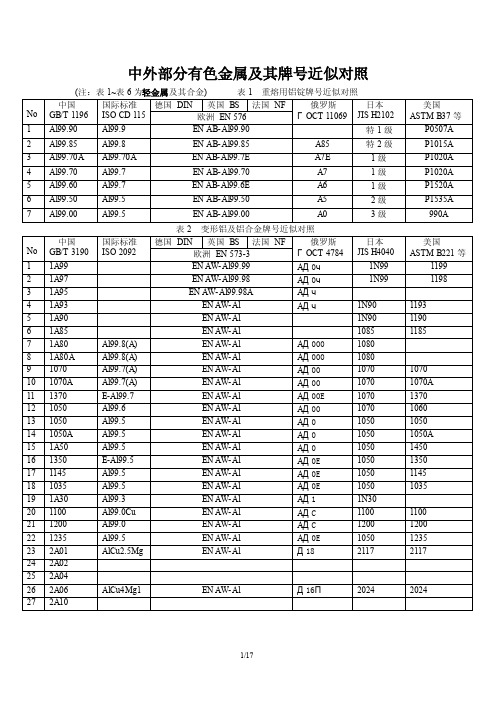
中外部分有色金属及其牌号近似对照
表2 变形铝及铝合金牌号近似对照
表4 原生镁锭牌号近似对照
表5 变形镁及镁合金牌号近似对照
续表5
表8 加工铜牌号近似对照
表10 加工青铜牌号近似对照
表12 铸造铜合金牌号近似对照
表13 锌锭牌号近似对照`
表14 加工锌及锌合金牌号近似对照
表15 压铸锌合金牌号近似对照
表16 压铸锌合金牌号近似对照
表17 锡及锡合金牌号近似对照
表18 铅及铅合金牌号近似对照
表22 铸造钛及钛合金牌号近似对照
表23 钨及其产品名称和牌号
表24 钨板(丝)牌号近似对照
表25 钼及其产品名称和牌号
表26 钼产品名称及牌号近似对照
(注:表27~表35为贵金属及其合金)表27 金锭及纯金(丝)牌号近对照
表29 银及纯银牌号近似对照
表30 银合金牌号近似对照
表31 银粉牌号
表32 海绵铂牌号近似对照
表34 铂合金牌号近似对照
表35 铱粉牌号近似对照
表36 铸造轴承合金牌号近似对照。
K2000说明书
控制对象
空调机组智能恒温控制系统
KJ 恒温控制 风机电机
空调机组智能恒温变风变水量控制系 KJ 恒温变风变
风机电机、水系统调节阀
统
水量控制
空调机组智能恒压控制系统
KJ 恒压控制 风机电机
空调机组智能恒压恒温恒湿控制系统 KJ 恒压恒温恒 风 机 电 机 、 水 系 统 调 节
湿控制
阀、蒸汽电磁阀
空调水泵智能恒温差控制系统
56
以 K2000-0015T3B 为例,产品外形及结构 部件如图 1-3 所示。壳体表面采用哑光工艺、 丝网印刷,光泽柔和、悦目。
金属外壳采用先进的 表面喷粉喷塑工艺,色泽考究、外观优美。
以 K2000-0220T3C 为例,产品外形及结构 部件如图 1-4 所示。 前面板采用可拆卸单边门轴结构,接线和维护 十分方便。
三、操作与显示 ····································································································15
3.1 液晶控制器······················································································· 15 3.2 功能参数设置 ··················································································· 17
自动循环运转 用户根据工艺要求编程输出频率模式
操作功能
频率设定 起/停控制
外部模拟信号(0~20mA)PI 控制 液晶控制盒控制、无源触点控制
2021年各种液位计说明介绍模板

公司简介欧阳光明(2021.03.07)北京铁强科技发展有限公司,位于我们伟大的首都——北京,是一家以工程仪表生产、研发为主的科技型企业,是一个极具活力与前景的多元化的新型民营企业。
公司技术力量雄厚,依靠北京的人才、技术、信息等优势,自2000年成立以来,通过短短七年多时间,就在仪器仪表生产制造领域内谱写一个又一个神话。
公司先后与北仪集团、德国西门子公司、美国麦克公司等仪表生产制造商进行广泛而深入的合作,在合作中公司产品的品质和质量得到很大提升。
同时,公司也在积极借鉴和引进国外先进技术和生产工艺,产品的科技含量不断提高、种类也在不断丰富。
另外,公司不断以新技术、新工艺、新材料、新设计理念设计生产品质高、性能优、用途广、使用寿命长的产品。
公司自主生产磁翻柱液位计、浮球液位计(液位开关)、钢带液位计、磁致伸缩液位计、微波物位计、电容式液位计、超声波液位计、音叉物位开关、电容式物位计、差压变送器等物位测量仪表。
同时,公司还经营流量仪表、压力仪表、温度仪表以及成分分析仪表等自动化测量、控制仪表。
经过几年的努力,公司发展了一支专业化、国际化、规模化的研发、生产、和管理团队。
公司现有员工100余名,其中有高级职称的技术人员5人、大专及以上各类专业人才80余名。
是“中国石化物资资源市场成员”单位;是“中国石油天然气集团公司一级供应网络”单位。
是众多国内外用户的高品质、可信赖的工业计量器具服务商。
公司一直秉承“技术为本,质量为先,笃信予人,益精致远”的经营理念,以“更强、更大、更实”为经营宗旨,开拓进取,务实创新,在做好产品生产和经营的基础上,还以打造中国仪表名牌为己任,投资开发有自主知识产权的产品。
在发展过程中,公司始终以快速的反应、精湛的技艺、热忱的服务及时为用户排忧解难,也因此得到了广大用户与社会各界的一致认可。
如今,公司全体员工正走专业化、特色化、精细化经营之道,并朝着两年时间内年销售额翻两番的目标奋力前进!北京铁强仪表科技发展有限公司产品选型样本目录01、磁翻柱液位计 (3)02、浮球液位计(液位开关) (5)03、防爆浮球液位开关 (7)04、玻璃板式液位计 (8)05、玻璃管式液位计 (10)06、钢带液位计 (12)07、重锤探测液位计 (14)08、超声波物位计 (15)09、智能雷达液位计 (17)10、导波雷达液位计 (19)11、电容式液位计 (21)12、射频导纳物位控制器 (23)13、音叉物位控制器 (25)14、磁致伸缩物位计 (27)15、压力液位变送器 (29)16、小型浮球液位计(液位开关) (31)17、常用客户名单 (32)注:我们是一家专业生产物位仪器仪表的科技型公司,随着市场的需求变化、我们的技术人员也会在保证质量的前提下,对产品进行改进,改造后的产品外观会有所变化、性能也会有所提高。
巴斯夫 Paliocrom Gold L 2000 安全技术说明书

安全技术说明书页: 1/8 巴斯夫安全技术说明书日期 / 修订: 14.09.2009版本: 5.0产品: Paliocrom* Gold L 2000(30047191/SDS_GEN_CN/ZH)印刷日期 23.09.20091. 物质/制剂及公司识别Paliocrom* Gold L 2000使用: 颜料用于涂漆,喷漆,和清漆工业。
公司:巴斯夫应用化工有限公司中国 上海浦东江心沙路300号邮政编码 200137电话: +86 21 3865-5265传真号: +86 21 3865-5268E-mail地址: ******************紧急情况资料:巴斯夫紧急热线中心(中国)电话: +86 21 5861-1199Company:BASF Auxiliary Chemicals Co., Ltd 300 Jiang Xin Sha RoadPu Dong Shanghai 200137, CHINATelephone: +86 21 3865-5265Telefax number: +86 21 3865-5268E-mail address: ******************Emergency information:Emergency Call Center (China):Telephone: +86 21 5861-11992. 危险性识别纯物质和混合物的分类:可燃固体: 分类3标签要素和警示性说明:巴斯夫安全技术说明书日期 / 修订: 14.09.2009版本: 5.0产品: Paliocrom* Gold L 2000(30047191/SDS_GEN_CN/ZH)印刷日期 23.09.2009警示词:警告危险性说明:可燃固体。
警示性说明(预防):地面接收容器或设备。
远离热源/火花/明火/热表面。
-禁止吸烟保持容器密封。
静电放电时采取预防措施。
使用防爆电气/通风/照明设备。
宝钢汽车产品标准 产品介绍 牌号命名方法 牌号对照表 化学成分 力学性能 订货标准

S220GD+Z, S220GD+ZF S250GD+Z, S250GD+ZF S280GD+Z (StE280-2Z)
S280GD+ZF S320GD+Z, S320GD+ZF S350GD+Z (StE345-2Z)
S350GD+ZF S550GD+Z, S550GD+ZF
结构用 Structure
低碳及超低碳钢 Low carbon and ultra-low carbon steel
标准号 Standard No.
电镀锌 Electro
加磷高强度钢
galvanizing High-strength phosphor steel
Q/BQB 430-2003
烘烤硬化高强度钢 High-strength bake hardening steel
标准号 Standard No.
Q/BQB 420-2003
牌号 Steel Grade DC51D+Z (St01Z, St02Z, St03Z) DC51D+ZF
DC52D+Z (St04Z), DC52D+ZF
DC53D+Z (St05Z), DC53D+ZF
用途及特点 Application and Features
一般用 Commercial purpose
冲压用 Drawing
深冲用 Deep drawing
DC54D+Z (St06Z), DC54D+ZF DD54D+Z (St06ZR)
DC56D+Z (St07Z), DC56D+ZF
2012产品技术参数OK11

455 684 970 1330 1570
731 820 1280
1960 600
1040
1438 1260
394.2 565 770 1081 1152 1510 1705? 2545 409.5 615.6 873 1197 1413 657.9 738 1152 1764 540 936 1294 1134
YQ3020-1 无 YQ3024-1 无
1.8 1.9
4.8 20*20 91 4.8 24*24 116
50 60
495 0 0 755 679.5 1065 958.5
550
YQ3028-1 无 YQ3032 -1 无
1.9 1.9
5 5
28*28 32*32
126
60
60
1330 1197 0
无 无 无 无 无 无
1.7 1.7 1.8 1.8 1.8 1.8
4 4 4 4 4 4
1.8 1.6 1.8 1.6 1.8 1.7 1.8 1.8 1.8 1.8 1.4 1.7 1.8 1.8 1.8 2 2 2 1.8 1.8 1.9 1.9 2.1 2.5 2.5 2.5 2.5 1.8 1.8 2 2 2 2.2 1.8 2.2 2.2 2.2 1.8
/ / / / / / 3.5 3.5 3.5 3.5 3.5 3.5 3.5 3.5 3.5 3.5 3.5 3.5 3.5 3.5 3.5 3.5 3.5 3.5 3.5 3.5 3.5 3.5 3.5 3.5 3.5 3.5 3.5 3.5 3.5 3.5 3.5 / / / / / / / /
2
1.9 1.9 2 2 2 2 2 2 5 4 4 4 4 4 4 4 4 4 4 4 4 4 4 4 4 4 4
5082-0012资料

DescriptionThis PIN diode chip is silicon dioxide or nitride passi-vated. The 5082-0012 has a planar construction. The fabrication processes are optimized for long term reliability and tightly controlled for uniformity in electrical performance.OutlineMaximum RatingsJunction Operating and StorageTemperature Range .............................-65°C to +150°C Soldering Temperature ..........+425°C for 1 min. max.5082-0012PIN Diode Chip for Hybrid MIC Switches/AttenuatorsData SheetFeatures•Low Series Resistance: 1.0Ω TypicalApplicationsThis general purpose PIN diode is intended for low power switching applications such as duplexers,antenna switching matrices, digital phase shifters, time multiplex filters, TR switches, pulse and amplitude modulators, limiters, leveling circuits, and attenuators.Electrical Specifications at T A = 25°CTypical ParametersNearest Typical Chip Equivalent Minimum Maximum Typical Reverse Part Packaged Breakdown Junction Series Typical Recovery Number Part No.VoltageCapacitance Resistance Lifetime Time 5082-5082-V BR (V)C j (pF)R S (Ω)τ (ns)t rr (ns)001230011500.12 1.0400100 Test V R = V BR V R = 50 V I F = 100 mA I F = 50 mA I F = 20 mA ConditionsMeasure f = 1 MHzf = 100 MHzI R = 250 mAV R = 10 V I R ≤ 10 mA90% RecoveryDimensions in millimeters (1/1000 inch)Assembly and Handling Procedures forPIN Chips1. StorageDevices should be stored in a dry nitrogen purged dessicator or equivalent.2. CleaningIf required, surface contamination may be removed with electronic grade solvents. Typical solvents, such as freon (T.F. or T.M.C.), acetone, deionized water, and methanol, or their locally approved equivalents, can be used singularly or in combinations. Typical cleaning times per solvent are one to three minutes. DI water and methanol should be used (in that order) in the final cleans. Final drying can be accomplished by placing the cleaned dice on clean filter paper and drying with an infrared lamp for 5-10 minutes. Acids such as hydrofluoric (HF), nitric (HN O3) and hydrochloric (HCl) should not be used.The effects of cleaning methods/solutions should be verified on small samples prior to submitting the entire lot.Following cleaning, dice should be either used in assembly (typically within a few hours) or stored in clean containers in a reducing atmosphere or a vacu-um chamber.3. Die Attacha. EutecticAuSn preform with stage temperature of 310°C for one minute max. AuGe preform with stage temperature of 390°C for one minute max.b. EpoxyFor epoxy die-attach, conductive silver-filled or gold-filled epoxies are recommended. This method can be used for all Avago PIN chips.4. Wire BondingEither ultrasonic or thermocompression bonding tech-niques can be employed. Suggested wire is pure gold, 0.7 to 1.5 mil diameter.For product information and a complete list of distributors, please go to our web site: Avago, Avago Technologies, and the A logo are trademarks of Avago Technologies, Pte. in the United States and other countries.Data subject to change. Copyright © 2006 Avago Technologies Pte. All rights reserved. Obsoletes 5965-8880E5989-4778EN February 23, 2006。
GD2000-管道杂项组件
单级节流杆 单级节流杆 单级节流杆 单级节流杆 单级节流杆 单级节流杆
启动疏水或其它降压系统 启动疏水或其它降压系统 启动疏水或其它降压系统 启动疏水或其它降压系统 启动疏水或其它降压系统 启动疏水或其它降压系统
指针型三向位移指示器 光电型三向位移指示器
水流指示器 水流指示器 水流指示器 水流指示器 水流指示器 水流指示器 水流指示器 水流指示器 水流指示器 水流指示器 水流指示器 水流指示器 水流指示器
管道杂项组件编制说明
1 疏水管用多级节流孔板
多级节流孔板用于蒸汽管道经常疏水,根据《管规》DL/T5054-1996,亚临界和超临界
参数机组的经常疏水都采用疏水阀。超高压及以下参数机组采用多级节流孔 板,因此此
次修编多级节流孔板在原《87 典管》的基础上,取消亚临界参数系列,增加次高压参数
系列。疏水管用多级节流孔板在原来《87 典管》的基础上局部改进,将两级之间的连接
次高压锅炉汽包安全阀消音器 次高压锅炉汽包安全阀消音器 次高压锅炉过热器安全阀消音器 次高压锅炉过热器安全阀消音器
中压锅炉汽包安全阀消音器 中压锅炉汽包安全阀消音器 中压锅炉过热器安全阀消音器 中压锅炉过热器安全阀消音器
- 444 -
管道杂项组件编制说明 管道杂项组件编制说明
13 MN1.6C12W400A 14 MN1.6C12W450 15 MN1.6C12W450A 16 MN1.6C12W500 17 MN1.6C12W500A
蠕胀测点及监察段
1
MEB
2
MEA
串联阀中间垫圈组件
1
MB10C12M
PN10
Q215-A Q215-A Q215-A Q215-A Q215-A
5082-K121-ID000资料
Features• Low Power Consumption • Industry Standard Size• Industry Standard Pinout • Choice of Character Size7.6 mm (0.30 in), 10 mm (0.40 in), 10.9 mm (0.43 in), 14.2 mm (0.56 in), 20 mm (0.80 in)• Choice of ColorsAlGaAs Red, High Efficiency Red (HER), Yellow, Green• Excellent Appearance Evenly Lighted Segments±50° Viewing Angle• Design FlexibilityCommon Anode or Common CathodeSingle and Dual DigitLeft and Right Hand Decimal Points±1. Overflow Character• Categorized for Luminous IntensityYellow and Green Categorized for ColorUse of Like Categories Yields a Uniform Display• Excellent for Long Digit String Multiplexing DescriptionThese low current seven segment displays are designed for applica-tions requiring low power consumption. They are tested and selected for their excellent low current characteristics to ensure that the segments are matched at low currents. Drive currents as low as 1 mA per segment are available.Pin for pin equivalent displays are also available in a standard current or high light ambient design. The standard current displays are available in all colors and are ideal for most applica-tions. The high light ambient displays are ideal for sunlight ambients or long string lengths. For additional information see the 7.6 mm Micro Bright Seven Segment Displays, 10 mm Seven Segment Displays, 7.6 mm/10.9 mm Seven Segment Displays, 14.2 mm Seven Segment Displays, 20 mm Seven Segment Displays, or High Light Ambient Seven Segment Displays data sheets.Low Current Seven SegmentDisplays Technical Data HDSP-335x SeriesHDSP-555x SeriesHDSP-751x SeriesHDSP-A10x Series HDSP-A80x Series HDSP-A90x Series HDSP-E10x Series HDSP-F10x Series HDSP-G10x Series HDSP-H10x Series HDSP-K12x, K70x Series HDSP-N10x SeriesHDSP-N40x SeriesDevicesAlGaAs HER Yellow Green Package HDSP-HDSP-HDSP-HDSP-Description Drawing A1017511A801A9017.6 mm Common Anode Right Hand Decimal A A1037513A803A9037.6 mm Common Cathode Right Hand Decimal B A1077517A807A9077.6 mm Common Anode ±1. Overflow C A1087518A808A9087.6 mm Common Cathode ±1. Overflow D F10110 mm Common Anode Right Hand Decimal E F10310 mm Common Cathode Right Hand Decimal F F10710 mm Common Anode ±1. Overflow G F10810 mm Common Cathode ±1. Overflow H G10110 mm Two Digit Common Anode Right Hand Decimal X G10310 mm Two Digit Common Cathode Right Hand Decimal Y E100335010.9 mm Common Anode Left Hand Decimal I E101335110.9 mm Common Anode Right Hand Decimal J E103335310.9 mm Common Cathode Right Hand Decimal K E106335610.9 mm Universal ±1. Overflow[1]L H101555114.2 mm Common Anode Right Hand Decimal M H103555314.2 mm Common Cathode Right Hand Decimal N H107555714.2 mm Common Anode ±1. Overflow O H108555814.2 mm Common Cathode ±1. Overflow P K121K70114.2 mm Two Digit Common Anode Right Hand Decimal R K123K70314.2 mm Two Digit Common Cathode Right Hand Decimal S N10020 mm Common Anode Left Hand Decimal Q N101N40120 mm Common Anode Right Hand Decimal T N103N40320 mm Common Cathode Right Hand Decimal U N10520 mm Common Cathode Left Hand Decimal V N106N40620 mm Universal ±1. Overflow[1]W Note:1. Universal pinout brings the anode and cathode of each segment’s LED out to separate pins. See internal diagrams L or W.Part Numbering System5082-x xx x-x x x xxHDSP-x xx x-x x x xxMechanical Options[1]00: No mechanical optionColor Bin Options[1,2]0: No color bin limitationMaximum Intensity Bin[1,2]0: No maximum intensity bin limitationMinimum Intensity Bin[1,2]0: No minimum intensity bin limitationDevice Configuration/Color[1]G: GreenDevice Specific Configuration[1]Refer to respective datasheetPackage[1]Refer to Respective datasheetNotes:1. For codes not listed in the figure above, please refer to the respective datasheet or contact your nearest Agilent representative fordetails.2. Bin options refer to shippable bins for a part-number. Color and Intensity Bins are typically restricted to 1 bin per tube (excep-tions may apply). Please refer to respective datasheet for specific bin limit information.Package DimensionsPackage Dimensions (cont.)Package Dimensions (cont.)*The Side View of package indicates Country of Origin.Package Dimensions (cont.)Package Dimensions (cont.)Package Dimensions (cont.)Internal Circuit DiagramInternal Circuit Diagram (cont.)Absolute Maximum RatingsAlGaAs Red - HDSP-HERA10X/E10X/H10X HDSP-751X/Yellow GreenK12X/N10X/N40X335X/555X/HDSP-A80X HDSP-A90X Description F10X, G10X Series K70X Series Series Series Units Average Power per Segment or DP375264mW Peak Forward Current per 45mA Segment or DPDC Forward Current per15[1]15[2]mA Segment or DPOperating Temperature Range-20 to +100-40 to +100°C Storage Temperature Range -55 to +100°C Reverse Voltage per Segment 3.0V or DPWave Soldering Temperature for 3Seconds (1.60 mm [0.063 in.] below 250°C seating body)Notes:1. Derate above 91°C at 0.53 mA/°C.2. Derate HER/Yellow above 80°C at 0.38 mA/°C and Green above 71°C at 0.31 mA/°C.Electrical/Optical Characteristics at T A = 25°CAlGaAs RedDeviceSeriesHDSP-Parameter Symbol Min.Typ.Max.Units Test Conditions315600I F = 1 mA A10x3600I F = 5 mA330650I F = 1 mAF10x, G10x3900I F = 5 mA390650I F = 1 mA E10x Luminous Intensity/Segment[1,2]I Vµcd(Digit Average)3900I F = 5 mA400700I F = 1 mAH10x, K12x4200I F = 5 mA270590I F = 1 mAN10x, N40x3500I F = 5 mA1.6I F = 1 mAForward Voltage/Segment or DP V F 1.7V I F = 5 mA1.82.2I F = 20 mA PkAll Devices Peak WavelengthλPEAK645nmDominant Wavelength[3]λd637nmReverse Voltage/Segment or DP[4]V R 3.015V I R = 100 µATemperature Coefficient of∆V F/°C-2 mV mV/°CV F/Segment or DPA10x255F10x, G10x320E10x340Thermal Resistance LED RθJ-PIN°C/W/SegH10x, K12x Junction-to-Pin400N10x, N40x430High Efficiency RedDeviceSeriesHDSP-Parameter Symbol Min.Typ.Max.Units Test Conditions160270I F = 2 mA 751x1050I F = 5 mA200300I F = 2 mA Luminous Intensity/Segment[1,2]I V mcd(Digit Average)1200I F = 5 mA335x, 555x,K70x270370I F = 2 mA1480I F = 5 mA1.6I F = 2 mAForward Voltage/Segment or DP V F 1.7V I F = 5 mA2.1 2.5I F = 20 mA Pk All Devices Peak WavelengthλPEAK635nmDominant Wavelength[3]λd626nmReverse Voltage/Segment or DP[4]V R 3.030V I R = 100 µATemperature Coefficient of∆V F/°C-2mV/°CV F/Segment or DP751x200335x Thermal Resistance LED RθJ-PIN280°C/WJunction-to-Pin555x, K70x345YellowDeviceSeriesHDSP-Parameter Symbol Min.Typ.Max.Units Test Conditions Luminous Intensity/Segment[1,2]250420I F = 4 mA(Digit Average)I V mcd1300I F = 10 mA1.7I F = 4 mAForward Voltage/Segment or DP V F 1.8V I F = 5 mA A80x2.1 2.5I F = 20 mA PkPeak WavelengthλPEAK583nmDominant Wavelength[3,5]λd581.5585592.5nmReverse Voltage/Segment or DP[4]V R 3.030V I R = 100 µATemperature Coefficient of∆V F/°C-2mV/°CV F/Segment or DPThermal Resistance LED RθJ-PIN200°C/WJunction-to-PinGreenDeviceSeriesHDSP-Parameter Symbol Min.Typ.Max.Units Test Conditions Luminous Intensity/Segment[1,2]250475I F = 4 mA(Digit Average)I V mcd1500I F = 10 mA1.9I F = 4 mAForward Voltage/Segment or DP V F 2.0V I F = 10 mA A90x2.1 2.5I F = 20 mA PkPeak WavelengthλPEAK566nmDominant Wavelength[3,5]λd571577nmReverse Voltage/Segment or DP[4]V R 3.030V I R = 100 µATemperature Coefficient of∆V F/°C-2mV/°CV F/Segment or DPThermal Resistance LED RθJ-PIN200°C/WJunction-to-PinNotes:1. Device case temperature is 25°C prior to the intensity measurement.2. The digits are categorized for luminous intensity. The intensity category is designated by a letter on the side of the package.3. The dominant wavelength, λd, is derived from the CIE chromaticity diagram and is the single wavelength which defines the color of thedevice.4. Typical specification for reference only. Do not exceed absolute maximum ratings.5. The yellow (HDSP-A800) and Green (HDSP-A900) displays are categorized for dominant wavelength. The category is designated by anumber adjacent to the luminous intensity category letter.AlGaAs RedIntensity Bin Limits (mcd)AlGaAs RedHDSP-A10xIV Bin Category Min.Max.E0.3150.520F0.4280.759G0.621 1.16H0.945 1.71I 1.40 2.56J 2.10 3.84K 3.14 5.75L 4.708.55HDSP-E10x/F10x/G10xIV Bin Category Min.Max.D0.3910.650E0.5320.923F0.755 1.39G 1.13 2.08H 1.70 3.14HDSP-H10x/K12xIV Bin Category Min.Max.C0.4150.690D0.5650.990E0.810 1.50F 1.20 2.20G 1.80 3.30H 2.73 5.00I 4.097.50HDSP-N10xIV Bin Category Min.Max.A0.2700.400B0.3250.500C0.4150.690D0.5650.990E0.810 1.50F 1.20 2.20G 1.80 3.30H 2.73 5.00I 4.097.50Intensity Bin Limits (mcd), continued HERHDSP-751xIV Bin Category Min.Max.B0.1600.240C0.2000.300D0.2500.385E0.3150.520F0.4280.759G0.621 1.16HDSP-751xIV Bin Category Min.Max.B0.2400.366C0.3000.477D0.3910.650E0.5320.923F0.755 1.39G 1.13 2.08H 1.70 3.14HDSP-555x/K70xIV Bin Category Min.Max.A0.2700.400B0.3250.500C0.4150.690D0.5650.990E0.810 1.50F 1.20 2.20G 1.80 3.30H 2.73 5.00I 4.097.50Intensity Bin Limits (mcd), continued YellowHDSP-A80xIV Bin Category Min.Max.D0.2500.385E0.3150.520F0.4250.760G0.625 1.14H0.940 1.70I 1.40 2.56J 2.10 3.84K 3.14 5.76L 4.718.64M7.0713.00N10.6019.40O15.9029.20P23.9043.80Q35.8065.60GreenHDSP-A90xIV Bin Category Min.Max.E0.3150.520F0.4250.760G0.625 1.14H0.940 1.70I 1.40 2.56J 2.10 3.84K 3.14 5.76L 4.718.64M7.0713.00N10.6019.40O15.9029.20P23.9043.80Q35.8065.60Electrical/OpticalFor more information on electrical/optical characteristics, please see Application Note 1005.Contrast Enhancement For information on contrast enhancement, please see Application Note 1015.Soldering/Cleaning Cleaning agents from the ketone family (acetone, methyl ethyl ketone, etc.) and from the chorinated hydrocarbon family (methylene chloride, trichloro-ethylene, carbon tetrachloride, etc.) are not recommended for cleaning LED parts. All of these various solvents attack or dissolve the encapsulating epoxies used to form the package of plastic LED parts.For information on soldering LEDs, please refer to Application Note 1027.Note:All categories are established for classification of products. Productsmay not be available in all categories. Please contact your localAgilent representatives for further clarification/information.Color Categories/semiconductorsFor product information and a complete list ofdistributors, please go to our web site.For technical assistance call:Americas/Canada: +1 (800) 235-0312 or(916) 788 6763Europe: +49 (0) 6441 92460China: 10800 650 0017Hong Kong: (+65) 6271 2451India, Australia, New Zealand: (+65) 6271 2394Japan: (+81 3) 3335-8152(Domestic/International), or0120-61-1280(Domestic Only)Korea: (+65) 6271 2194Malaysia, Singapore: (+65) 6271 2054Taiwan: (+65) 6271 2654Data subject to change.Copyright © 2005 Agilent Technologies, Inc.Obsoletes 5988-8412ENJanuary 19, 20055989-0080EN。
- 1、下载文档前请自行甄别文档内容的完整性,平台不提供额外的编辑、内容补充、找答案等附加服务。
- 2、"仅部分预览"的文档,不可在线预览部分如存在完整性等问题,可反馈申请退款(可完整预览的文档不适用该条件!)。
- 3、如文档侵犯您的权益,请联系客服反馈,我们会尽快为您处理(人工客服工作时间:9:00-18:30)。
Features• Low Power Consumption • Industry Standard Size• Industry Standard Pinout • Choice of Character Size7.6 mm (0.30 in), 10 mm (0.40 in), 10.9 mm (0.43 in), 14.2 mm (0.56 in), 20 mm (0.80 in)• Choice of ColorsAlGaAs Red, High Efficiency Red (HER), Yellow, Green• Excellent Appearance Evenly Lighted Segments±50° Viewing Angle• Design FlexibilityCommon Anode or Common CathodeSingle and Dual DigitLeft and Right Hand Decimal Points±1. Overflow Character• Categorized for Luminous IntensityYellow and Green Categorized for ColorUse of Like Categories Yields a Uniform Display• Excellent for Long Digit String Multiplexing DescriptionThese low current seven segment displays are designed for applica-tions requiring low power consumption. They are tested and selected for their excellent low current characteristics to ensure that the segments are matched at low currents. Drive currents as low as 1 mA per segment are available.Pin for pin equivalent displays are also available in a standard current or high light ambient design. The standard current displays are available in all colors and are ideal for most applica-tions. The high light ambient displays are ideal for sunlight ambients or long string lengths. For additional information see the 7.6 mm Micro Bright Seven Segment Displays, 10 mm Seven Segment Displays, 7.6 mm/10.9 mm Seven Segment Displays, 14.2 mm Seven Segment Displays, 20 mm Seven Segment Displays, or High Light Ambient Seven Segment Displays data sheets.Low Current Seven SegmentDisplays Technical Data HDSP-335x SeriesHDSP-555x SeriesHDSP-751x SeriesHDSP-A10x Series HDSP-A80x Series HDSP-A90x Series HDSP-E10x Series HDSP-F10x Series HDSP-G10x Series HDSP-H10x Series HDSP-K12x, K70x Series HDSP-N10x SeriesHDSP-N40x SeriesDevicesAlGaAs HER Yellow Green Package HDSP-HDSP-HDSP-HDSP-Description Drawing A1017511A801A9017.6 mm Common Anode Right Hand Decimal A A1037513A803A9037.6 mm Common Cathode Right Hand Decimal B A1077517A807A9077.6 mm Common Anode ±1. Overflow C A1087518A808A9087.6 mm Common Cathode ±1. Overflow D F10110 mm Common Anode Right Hand Decimal E F10310 mm Common Cathode Right Hand Decimal F F10710 mm Common Anode ±1. Overflow G F10810 mm Common Cathode ±1. Overflow H G10110 mm Two Digit Common Anode Right Hand Decimal X G10310 mm Two Digit Common Cathode Right Hand Decimal Y E100335010.9 mm Common Anode Left Hand Decimal I E101335110.9 mm Common Anode Right Hand Decimal J E103335310.9 mm Common Cathode Right Hand Decimal K E106335610.9 mm Universal ±1. Overflow[1]L H101555114.2 mm Common Anode Right Hand Decimal M H103555314.2 mm Common Cathode Right Hand Decimal N H107555714.2 mm Common Anode ±1. Overflow O H108555814.2 mm Common Cathode ±1. Overflow P K121K70114.2 mm Two Digit Common Anode Right Hand Decimal R K123K70314.2 mm Two Digit Common Cathode Right Hand Decimal S N10020 mm Common Anode Left Hand Decimal Q N101N40120 mm Common Anode Right Hand Decimal T N103N40320 mm Common Cathode Right Hand Decimal U N10520 mm Common Cathode Left Hand Decimal V N106N40620 mm Universal ±1. Overflow[1]W Note:1. Universal pinout brings the anode and cathode of each segment’s LED out to separate pins. See internal diagrams L or W.Part Numbering System5082-x xx x-x x x xxHDSP-x xx x-x x x xxMechanical Options[1]00: No mechanical optionColor Bin Options[1,2]0: No color bin limitationMaximum Intensity Bin[1,2]0: No maximum intensity bin limitationMinimum Intensity Bin[1,2]0: No minimum intensity bin limitationDevice Configuration/Color[1]G: GreenDevice Specific Configuration[1]Refer to respective datasheetPackage[1]Refer to Respective datasheetNotes:1. For codes not listed in the figure above, please refer to the respective datasheet or contact your nearest Agilent representative fordetails.2. Bin options refer to shippable bins for a part-number. Color and Intensity Bins are typically restricted to 1 bin per tube (excep-tions may apply). Please refer to respective datasheet for specific bin limit information.Package DimensionsPackage Dimensions (cont.)Package Dimensions (cont.)*The Side View of package indicates Country of Origin.Package Dimensions (cont.)Package Dimensions (cont.)Package Dimensions (cont.)Internal Circuit DiagramInternal Circuit Diagram (cont.)Absolute Maximum RatingsAlGaAs Red - HDSP-HERA10X/E10X/H10X HDSP-751X/Yellow GreenK12X/N10X/N40X335X/555X/HDSP-A80X HDSP-A90X Description F10X, G10X Series K70X Series Series Series Units Average Power per Segment or DP375264mW Peak Forward Current per 45mA Segment or DPDC Forward Current per15[1]15[2]mA Segment or DPOperating Temperature Range-20 to +100-40 to +100°C Storage Temperature Range -55 to +100°C Reverse Voltage per Segment 3.0V or DPWave Soldering Temperature for 3Seconds (1.60 mm [0.063 in.] below 250°C seating body)Notes:1. Derate above 91°C at 0.53 mA/°C.2. Derate HER/Yellow above 80°C at 0.38 mA/°C and Green above 71°C at 0.31 mA/°C.Electrical/Optical Characteristics at T A = 25°CAlGaAs RedDeviceSeriesHDSP-Parameter Symbol Min.Typ.Max.Units Test Conditions315600I F = 1 mA A10x3600I F = 5 mA330650I F = 1 mAF10x, G10x3900I F = 5 mA390650I F = 1 mA E10x Luminous Intensity/Segment[1,2]I Vµcd(Digit Average)3900I F = 5 mA400700I F = 1 mAH10x, K12x4200I F = 5 mA270590I F = 1 mAN10x, N40x3500I F = 5 mA1.6I F = 1 mAForward Voltage/Segment or DP V F 1.7V I F = 5 mA1.82.2I F = 20 mA PkAll Devices Peak WavelengthλPEAK645nmDominant Wavelength[3]λd637nmReverse Voltage/Segment or DP[4]V R 3.015V I R = 100 µATemperature Coefficient of∆V F/°C-2 mV mV/°CV F/Segment or DPA10x255F10x, G10x320E10x340Thermal Resistance LED RθJ-PIN°C/W/SegH10x, K12x Junction-to-Pin400N10x, N40x430High Efficiency RedDeviceSeriesHDSP-Parameter Symbol Min.Typ.Max.Units Test Conditions160270I F = 2 mA 751x1050I F = 5 mA200300I F = 2 mA Luminous Intensity/Segment[1,2]I V mcd(Digit Average)1200I F = 5 mA335x, 555x,K70x270370I F = 2 mA1480I F = 5 mA1.6I F = 2 mAForward Voltage/Segment or DP V F 1.7V I F = 5 mA2.1 2.5I F = 20 mA Pk All Devices Peak WavelengthλPEAK635nmDominant Wavelength[3]λd626nmReverse Voltage/Segment or DP[4]V R 3.030V I R = 100 µATemperature Coefficient of∆V F/°C-2mV/°CV F/Segment or DP751x200335x Thermal Resistance LED RθJ-PIN280°C/WJunction-to-Pin555x, K70x345YellowDeviceSeriesHDSP-Parameter Symbol Min.Typ.Max.Units Test Conditions Luminous Intensity/Segment[1,2]250420I F = 4 mA(Digit Average)I V mcd1300I F = 10 mA1.7I F = 4 mAForward Voltage/Segment or DP V F 1.8V I F = 5 mA A80x2.1 2.5I F = 20 mA PkPeak WavelengthλPEAK583nmDominant Wavelength[3,5]λd581.5585592.5nmReverse Voltage/Segment or DP[4]V R 3.030V I R = 100 µATemperature Coefficient of∆V F/°C-2mV/°CV F/Segment or DPThermal Resistance LED RθJ-PIN200°C/WJunction-to-PinGreenDeviceSeriesHDSP-Parameter Symbol Min.Typ.Max.Units Test Conditions Luminous Intensity/Segment[1,2]250475I F = 4 mA(Digit Average)I V mcd1500I F = 10 mA1.9I F = 4 mAForward Voltage/Segment or DP V F 2.0V I F = 10 mA A90x2.1 2.5I F = 20 mA PkPeak WavelengthλPEAK566nmDominant Wavelength[3,5]λd571577nmReverse Voltage/Segment or DP[4]V R 3.030V I R = 100 µATemperature Coefficient of∆V F/°C-2mV/°CV F/Segment or DPThermal Resistance LED RθJ-PIN200°C/WJunction-to-PinNotes:1. Device case temperature is 25°C prior to the intensity measurement.2. The digits are categorized for luminous intensity. The intensity category is designated by a letter on the side of the package.3. The dominant wavelength, λd, is derived from the CIE chromaticity diagram and is the single wavelength which defines the color of thedevice.4. Typical specification for reference only. Do not exceed absolute maximum ratings.5. The yellow (HDSP-A800) and Green (HDSP-A900) displays are categorized for dominant wavelength. The category is designated by anumber adjacent to the luminous intensity category letter.AlGaAs RedIntensity Bin Limits (mcd)AlGaAs RedHDSP-A10xIV Bin Category Min.Max.E0.3150.520F0.4280.759G0.621 1.16H0.945 1.71I 1.40 2.56J 2.10 3.84K 3.14 5.75L 4.708.55HDSP-E10x/F10x/G10xIV Bin Category Min.Max.D0.3910.650E0.5320.923F0.755 1.39G 1.13 2.08H 1.70 3.14HDSP-H10x/K12xIV Bin Category Min.Max.C0.4150.690D0.5650.990E0.810 1.50F 1.20 2.20G 1.80 3.30H 2.73 5.00I 4.097.50HDSP-N10xIV Bin Category Min.Max.A0.2700.400B0.3250.500C0.4150.690D0.5650.990E0.810 1.50F 1.20 2.20G 1.80 3.30H 2.73 5.00I 4.097.50Intensity Bin Limits (mcd), continued HERHDSP-751xIV Bin Category Min.Max.B0.1600.240C0.2000.300D0.2500.385E0.3150.520F0.4280.759G0.621 1.16HDSP-751xIV Bin Category Min.Max.B0.2400.366C0.3000.477D0.3910.650E0.5320.923F0.755 1.39G 1.13 2.08H 1.70 3.14HDSP-555x/K70xIV Bin Category Min.Max.A0.2700.400B0.3250.500C0.4150.690D0.5650.990E0.810 1.50F 1.20 2.20G 1.80 3.30H 2.73 5.00I 4.097.50Intensity Bin Limits (mcd), continued YellowHDSP-A80xIV Bin Category Min.Max.D0.2500.385E0.3150.520F0.4250.760G0.625 1.14H0.940 1.70I 1.40 2.56J 2.10 3.84K 3.14 5.76L 4.718.64M7.0713.00N10.6019.40O15.9029.20P23.9043.80Q35.8065.60GreenHDSP-A90xIV Bin Category Min.Max.E0.3150.520F0.4250.760G0.625 1.14H0.940 1.70I 1.40 2.56J 2.10 3.84K 3.14 5.76L 4.718.64M7.0713.00N10.6019.40O15.9029.20P23.9043.80Q35.8065.60Electrical/OpticalFor more information on electrical/optical characteristics, please see Application Note 1005.Contrast Enhancement For information on contrast enhancement, please see Application Note 1015.Soldering/Cleaning Cleaning agents from the ketone family (acetone, methyl ethyl ketone, etc.) and from the chorinated hydrocarbon family (methylene chloride, trichloro-ethylene, carbon tetrachloride, etc.) are not recommended for cleaning LED parts. All of these various solvents attack or dissolve the encapsulating epoxies used to form the package of plastic LED parts.For information on soldering LEDs, please refer to Application Note 1027.Note:All categories are established for classification of products. Productsmay not be available in all categories. Please contact your localAgilent representatives for further clarification/information.Color Categories/semiconductorsFor product information and a complete list ofdistributors, please go to our web site.For technical assistance call:Americas/Canada: +1 (800) 235-0312 or(916) 788 6763Europe: +49 (0) 6441 92460China: 10800 650 0017Hong Kong: (+65) 6271 2451India, Australia, New Zealand: (+65) 6271 2394Japan: (+81 3) 3335-8152(Domestic/International), or0120-61-1280(Domestic Only)Korea: (+65) 6271 2194Malaysia, Singapore: (+65) 6271 2054Taiwan: (+65) 6271 2654Data subject to change.Copyright © 2005 Agilent Technologies, Inc.Obsoletes 5988-8412ENJanuary 19, 20055989-0080EN。