ZXTN25020BFHTA;中文规格书,Datasheet资料
拓顿(Eaton)电气断路器电流传感器和ating插座替换套件说明书
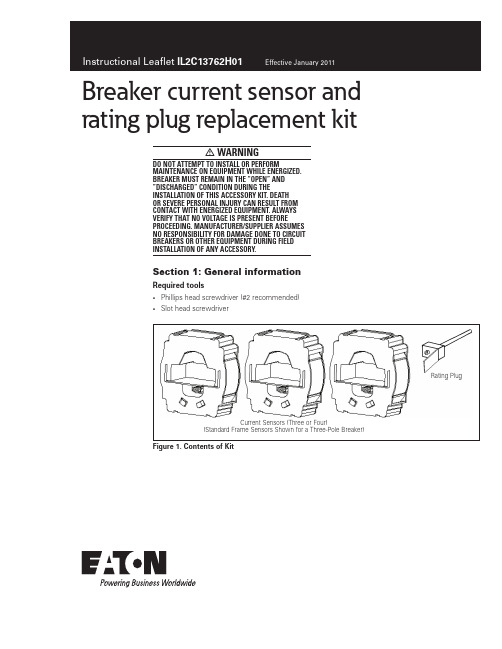
Instructional Leaflet IL2C13762H01
Effective January 2011
Figure 4. Step 6
eaton corporation
3
InstruChain Management is a registered trademark of Eaton Corporation.
All other trademarks are property of their respective owners.
Instructional Leaflet IL2C13762H01
Effective January 2011
Breaker current sensor and rating plug replacement kit
warning
Do NOT attempt to install or perform maintenance on equipment while energized. Breaker must remain in the “OPEN” and ”DISCHARGED” condition during the installation of this accessory kit. Death or severe personal injury can result from contact with energized equipment. Always verify that no voltage is present before proceeding. Manufacturer/Supplier assumes no responsibility for damage done to circuit breakers or other equipment during field installation of any accessory.
ZXMD63N02XTA;ZXMD63N02XTC;中文规格书,Datasheet资料

DUAL 20V N-CHANNEL ENHANCEMENT MODE MOSFETProduct SummaryV (BR)DSSR DS(ON) Package I DT A = +25°C(Notes 5 & 6)20V130m Ω @ V GS = 4.5VMSOP-82.5A150m Ω @ V GS = 2.7V2.3ADescriptionThis MOSFET has been designed to minimize the on-state resistance (R DS(on)) and yet maintain superior switching performance, making it ideal for high efficiency power management applications.Applications• DC-DC Converters• Power Management functions • Motor Control • Disconnect SwitchesFeatures• Low On-Resistance • Low Threshold • Fast Switching Speed • Low Gate Drive• Totally Lead-Free & Fully RoHS Compliant (Notes 1 & 2) • Halogen and Antimony Free. “Green” Device (Note 3) • Qualified to AEC-Q101 Standards for High ReliabilityMechanical Data• Case: MSOP-8 • Case Material: Molded Plastic, “Green” Molding Compound.UL Flammability Classification Rating 94V-0 • Moisture Sensitivity: Level 1 per J-STD-020 • Terminals: Matte Tin Finish •Weight: 0.008 grams (approximate)Ordering Information (Note 4)Product Marking Reel size (inches) Tape width (mm)Quantity per reelZXMD63N02XTA ZXM63N02 7 12 1,000 ZXMD63N02XTC ZXM63N02 1312 4,000Notes: 1. No purposely added lead. Fully EU Directive 2002/95/EC (RoHS) & 2011/65/EU (RoHS 2) compliant.2. See for more information about Diodes Incorporated’s definitions of Halogen and Antimony free,"Green" and Lead-Free.3. Halogen and Antimony free "Green” products are defined as those which contain <900ppm bromine, <900ppm chlorine (<1500ppm total Br + Cl) and <1000ppm antimony compounds.4. For packaging details, go to our website at Marking Informatione3Top ViewMSOP8Device SymbolTop View Pin-OutZXM63N02 = Product type Marking CodeMaximum Ratings(@T A = +25°C, unless otherwise specified.)Characteristic Symbol Value UnitDrain-Source Voltage V DSS20 V Gate-Source Voltage V GSS±12 VContinuous Drain Current SteadyState@ V GS = 10V;T A= +25°C (Note 5 & 6)@ V GS = 10V;T A= +70°C (Note 5 & 6)@ V GS = 10V;T A= +100°C (Note 5 & 6)I D2.51.90.78APulsed Drain Current (Notes 6 & 7) I DM19 AContinuous Source Current (Body Diode) (Notes 5 & 6) I S 1.5 APulsed Source Current (Body Diode) (Notes 6 & 7) I SM19 AThermal CharacteristicsCharacteristic SymbolValueUnitPower Dissipation (Notes 6 & 8)P D0.87W (Notes 5 & 6) 1.25(Notes 8 & 9) 1.04Thermal Resistance, Junction to Ambient (Notes 6 & 8)RθJA143°C/W (Notes 5 & 6)100(Notes 8 & 9)120Thermal Resistance, Junction to Leads (Note 10) RθJL84.9 °C/W Operating and Storage Temperature Range T J, T STG-55 to +150 °CNotes: 5. For a device surface mounted on FR4 PCB measured at t ≤ 10 sec.6. For device with one active die.7. Repetitive rating - 25mm x 25mm FR4 PCB, D = 0.02, pulse width 300μs – pulse width limited by maximum junction temperature.8. For a device surface mounted on 25mm x 25mm FR4 PCB with high coverage of single sided 1oz copper, in still air conditions.9. For device with two active die running at equal power.10. Thermal resistance from junction to solder-point (at the end of the drain lead).Thermal Characteristics204060801001201401600.00.10.20.30.40.50.60.70.80.9Derating CurveTemperature (°C)M a x P o w e r D i s s i p a t i o n (W )Transient Thermal Impedance T h e r m a l Re s i s t a n c e (°C /W )Pulse Width (s)Pulse Power DissipationPulse Width (s)M a x i m u m P o w e r (W )Electrical Characteristics (@T A = +25°C, unless otherwise specified.)CharacteristicSymbol Min Typ Max Unit Test ConditionOFF CHARACTERISTICSDrain-Source Breakdown VoltageBV DSS 20 - - V V GS = 0V, I D = 250μA Zero Gate Voltage Drain Current T J = +25°C I DSS - - 1.0 µA V DS = 20V, V GS = 0V Gate-Source Leakage I GSS - - 100 nA V GS = ±12V, V DS = 0V ON CHARACTERISTICS Gate Threshold VoltageV GS(th) 0.7 - 3 V V DS = V GS , I D = 250μAStatic Drain-Source On-Resistance (Note 11) R DS (ON) -65 130 m Ω V GS = 4.5V, I D = 1.7A90 150 V GS = 2.7V, I D = 0.85AForward Transconductance (Notes 11 & 13) g fs 2.6 - - S V DS = 10V, I D = 0.85A Diodes Forward Voltage (Note 11) V SD - 0.85 0.95 V T J = 25°C, I S = 1.7A, V GS = 0V DYNAMIC CHARACTERISTICS Input Capacitance (Note 12 & 13) C iss - 350 700pFV DS = 15V, V GS = 0V,f = 1.0MHzOutput Capacitance (Notes 12 & 13)C oss - 120 250 Reverse Transfer Capacitance (Notes 12 & 13) C rss - 50 100 Gate Resistance (Notes 12 & 13) R g - 3.8 7.6 Ω f = 1MHz, V GS = 0V, V DS = 0V Total Gate Charge (Notes 12 & 13) Q g - 4.5 6nCV GS = 4.5V, V DS = 16V,I D = 1.7AGate-Source Charge (Notes 12 & 13) Q gs - 0.5 0.65 Gate-Drain Charge (Notes 12 & 13) Q gd - 2 2.5 Reverse Recovery Time (Note 13) t rr - 15 30 ns T J = +25°C, I F = 1.7A,di/dt = 100A/µs Reverse Recovery Charge (Note 13) Q rr - 5.9 - nCTurn-On Delay Time (Notes 12 & 13) t D(on) - 3.4 - nsV DD = 10V, I D = 1.7A,R G = 6Ω, R D = 5.7Ω, Turn-On Rise Time (Notes 12 & 13) t r - 8.1 - Turn-Off Delay Time (Notes 12 & 13) t D(off) - 13.5 - Turn-Off Fall Time (Notes 12 & 13)t f- 9.1 -Notes:11. Measured under pulsed conditions. Pulse width ≤ 300μs; duty cycle ≤2%. 12. Switching characteristics are independent of operating junction temperature. 13. For design aid only, not subject to production testing.Typical CharacteristicsTypical Characteristics (cont.)Test CircuitsPackage Outline DimensionsSuggested Pad LayoutMSOP-8Dim Min Max Typ A - 1.10 - A1 0.050.15 0.10 A2 0.750.95 0.86 A3 0.290.49 0.39 b 0.220.38 0.30 c 0.080.23 0.15 D 2.90 3.10 3.00 E 4.70 5.10 4.90 E1 2.90 3.10 3.00 E3 2.85 3.05 2.95 e - - 0.65 L 0.400.80 0.60 a 0° 8° 4° x - - 0.750 y - - 0.750 All Dimensions in mmDimensions Value (in mm)C 0.650 X 0.450 Y 1.350 Y15.300Detail CIMPORTANT NOTICEDIODES INCORPORATED MAKES NO WARRANTY OF ANY KIND, EXPRESS OR IMPLIED, WITH REGARDS TO THIS DOCUMENT, INCLUDING, BUT NOT LIMITED TO, THE IMPLIED WARRANTIES OF MERCHANTABILITY AND FITNESS FOR A PARTICULAR PURPOSE (AND THEIR EQUIVALENTS UNDER THE LAWS OF ANY JURISDICTION).Diodes Incorporated and its subsidiaries reserve the right to make modifications, enhancements, improvements, corrections or other changes without further notice to this document and any product described herein. Diodes Incorporated does not assume any liability arising out of the application or use of this document or any product described herein; neither does Diodes Incorporated convey any license under its patent or trademark rights, nor the rights of others. Any Customer or user of this document or products described herein in such applications shall assume all risks of such use and will agree to hold Diodes Incorporated and all the companies whose products are represented on Diodes Incorporated website, harmless against all damages.Diodes Incorporated does not warrant or accept any liability whatsoever in respect of any products purchased through unauthorized sales channel. Should Customers purchase or use Diodes Incorporated products for any unintended or unauthorized application, Customers shall indemnify and hold Diodes Incorporated and its representatives harmless against all claims, damages, expenses, and attorney fees arising out of, directly or indirectly, any claim of personal injury or death associated with such unintended or unauthorized application.Products described herein may be covered by one or more United States, international or foreign patents pending. Product names and markings noted herein may also be covered by one or more United States, international or foreign trademarks.LIFE SUPPORTDiodes Incorporated products are specifically not authorized for use as critical components in life support devices or systems without the express written approval of the Chief Executive Officer of Diodes Incorporated. As used herein:A. Life support devices or systems are devices or systems which:1. are intended to implant into the body, or2. support or sustain life and whose failure to perform when properly used in accordance with instructions for use provided in thelabeling can be reasonably expected to result in significant injury to the user.B. A critical component is any component in a life support device or system whose failure to perform can be reasonably expected to cause thefailure of the life support device or to affect its safety or effectiveness.Customers represent that they have all necessary expertise in the safety and regulatory ramifications of their life support devices or systems, and acknowledge and agree that they are solely responsible for all legal, regulatory and safety-related requirements concerning their products and any use of Diodes Incorporated products in such safety-critical, life support devices or systems, notwithstanding any devices- or systems-related information or support that may be provided by Diodes Incorporated. Further, Customers must fully indemnify Diodes Incorporated and its representatives against any damages arising out of the use of Diodes Incorporated products in such safety-critical, life support devices or systems.Copyright © 2012, Diodes Incorporated分销商库存信息:DIODESZXMD63N02XTA ZXMD63N02XTC。
IRFP250NPBF;中文规格书,Datasheet资料
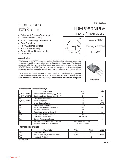
IRFP250NPbFHEXFET ® Power MOSFET08/18/10ParameterMax.UnitsI D @ T C = 25°C Continuous Drain Current, V GS @ 10V 30I D @ T C = 100°C Continuous Drain Current, V GS @ 10V 21A I DMPulsed Drain Current 120P D @T C = 25°C Power Dissipation 214W Linear Derating Factor 1.4W/°C V GS Gate-to-Source Voltage± 20V E AS Single Pulse Avalanche Energy 315mJ I AR Avalanche Current30A E AR Repetitive Avalanche Energy 21mJ dv/dt Peak Diode Recovery dv/dt 8.6V/ns T J Operating Junction and-55 to +175T STGStorage Temperature RangeSoldering Temperature, for 10 seconds 300 (1.6mm from case )°CMounting torque, 6-32 or M3 srew10 lbf•in (1.1N•m)Absolute Maximum RatingsParameterTyp.Max.UnitsR θJC Junction-to-Case–––0.7R θCS Case-to-Sink, Flat, Greased Surface 0.24–––°C/WR θJAJunction-to-Ambient–––40Thermal Resistance 1Descriptionl Advanced Process Technology l Dynamic dv/dt Ratingl 175°C Operating Temperature l Fast Switchingl Fully Avalanche Rated l Ease of Parallelingl Simple Drive Requirements TO-247AClLead-FreePD - 95007AIRFP250NPbFSource-Drain Ratings and CharacteristicsStarting T J = 25°C, L = 1.9mHR G = 25Ω, I AS = 18A. (See Figure 12)Repetitive rating; pulse width limited by max. junction temperature. (See Fig. 11)Notes:I SD ≤ 18A , di/d t ≤ 374A/µs, V DD ≤ V (BR)DSS ,T J ≤ 175°CPulse width ≤ 300µs; duty cycle ≤ 2%.Electrical Characteristics @ T = 25°C (unless otherwise specified)IRFP250NPbF 3Vs. TemperatureIRFP250NPbF4Fig 5. Typical Capacitance Vs.Drain-to-Source VoltageFig 6.Gate-to-Source VoltageForward VoltageTypical Gate Charge Vs.1101001000V DS , Drain-to-Source Voltage (V)010002000300040005000C , C a p a c i t a n c e (p F )IRFP250NPbF5Fig 9. Maximum Drain Current Vs.Fig 10a. Switching Time Test CircuitV V d(on)rd(off)fFig 10b. Switching Time WaveformsFig 11. Maximum Effective Transient Thermal Impedance, Junction-to-CaseDDIRFP250NPbF6VDSCurrent Sampling Resistors10 VFig 13b. Gate Charge Test CircuitFig 13a. Basic Gate Charge Waveform Fig 12b. Unclamped Inductive WaveformsI ASVs. Drain CurrentV DDIRFP250NPbF7Fig 14. For N-Channel HEXFETS* V GS = 5V for Logic Level DevicesPeak Diode Recovery dv/dt Test CircuitV DDIRFP250NPbFData and specifications subject to change without notice.233 Kansas St., El Segundo, California 90245, USA Tel: (310) 252-7105TAC Fax: (310) 252-7903Visit us at for sales contact information .08/2010分销商库存信息: IRIRFP250NPBF。
STTH6003CW;中文规格书,Datasheet资料
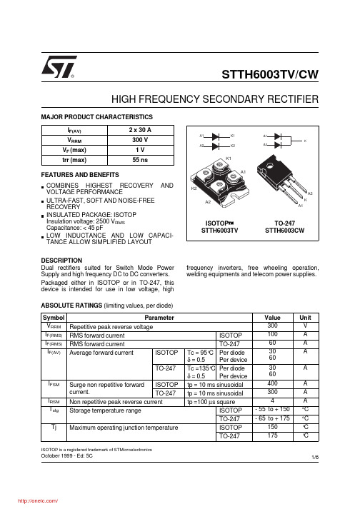
STTH6003TV/CWOctober 1999 - Ed: 5CHIGH FREQUENCY SECONDARY RECTIFIER®Dual rectifiers suited for Switch Mode Power Supply and high frequency DC to DC converters.Packaged either in ISOTOP or in TO-247, this device is intended for use in low voltage, high frequency inverters, free wheeling operation,welding equipments and telecom power supplies.DESCRIPTIONCOMBINES HIGHEST RECOVERY AND VOLTAGE PERFORMANCEULTRA-FAST, SOFT AND NOISE-FREE RECOVERYINSULATED PACKAGE: ISOTOP Insulation voltage: 2500 V RMS Capacitance: < 45 pFLOW INDUCTANCE AND LOW CAPACI-TANCE ALLOW SIMPLIFIED LAYOUT FEATURES AND BENEFITSSymbol ParameterValue Unit V RRM Repetitive peak reverse voltage 300V I F(RMS)RMS forward current ISOTOP 100A I F(RMS)RMS forward current TO-24760A I F(AV)Average forward current ISOTOPTc = 95°C δ = 0.5Per diode Per device 3060A TO-247Tc =135°C δ = 0.5Per diode Per device 3060A I FSM Surge non repetitive forward current.ISOTOP tp = 10 ms sinusoidal 400A TO-247tp = 10 ms sinusoidal 300A I RSMNon repetitive peak reverse current tp =100 µs square4A T stg Storage temperature rangeISOTOP - 55 to + 150°C TO-247- 65 to + 175°C TjMaximum operating junction temperatureISOTOP 150°C TO-247175°CABSOLUTE RATINGS (limiting values, per diode)I F(AV) 2 x 30 A V RRM 300 V V F (max) 1 V trr (max)55 nsMAJOR PRODUCT CHARACTERISTICSA1K1K2A2A1A2K1K2ISOTOP ™STTH6003TV ISOTOP is a registered trademark of STMicroelectronicsA1K A2A1A2KTO-247STTH6003CW1/6Symbol Parameter Tests conditionsMin.Typ.Max.Unit I R *Reverse leakage currentV R = 300 VTj = 25°C 60µATj = 125°C60600V F **Forward voltage dropI F = 30 ATj = 25°C 1.25V Tj = 125°C0.851Pulse test : * tp = 5 ms, δ < 2 % ** tp = 380 µs, δ < 2%To evaluate the maximum conduction losses use the following equation:P = 0.75 x I F(AV) + 0.008 x I F 2(RMS)STATIC ELECTRICAL CHARACTERISTICS (per diode)Symbol ParameterValue Unit R th (j-c)Junction to caseISOTOP Per diodeTotal 1.40.75°C/WTO-247Per diode Total 10.55R th (c)Coupling0.1When the diodes 1 and 2 are used simultaneously:∆Tj (diode 1) = P (diode 1) x R th(j-c) (per diode) + P (diode 2) x R th(C)THERMAL RESISTANCES Symbol Tests conditionsMin.Typ.Max.Unit trrI F = 0.5 A Irr = 0.25 A I R = 1A Tj = 25°C40nsI F= 1 A dI F /dt = - 50 A/µs V R = 30 V 55tfr I F = 30 A dI F /dt = 200 A/µs Tj = 25°C 350ns V FP V FR = 1.1 x V F max.5V S factor Vcc = 200 V I F = 30 A Tj = 125°C0.3-I RMdI F /dt = 200 A/µs11A RECOVERY CHARACTERISTICS STTH6003TV/CW2/65101520253035400510152025303540IF(av) (A)P1(W)Tδ=tp/Ttpδ= 1δ= 0.5δ= 0.2δ= 0.1δ= 0.05Fig. 1: Conduction losses versus average current (per diode).0.20.40.60.81.01.21.41.61.82.02.22.42.6110100VFM(V)IFM(A)Tj=125°C T ypical valuesTj=25°C Maximum valuesTj=125°C Maximum valuesFig. 2: Forward voltage drop versus forward current (maximum values , per diode).05010015020025030035040045050020406080100120140160180trr(ns)VR=200V Tj=125°CIF=2*IF(av)IF=IF(av)IF=0.5*IF(av)dIF/dt(A/µs)Fig. 5: Reverse recovery time versus dI F /dt (90%confidence, per diode).50100150200250300350400450500246810121416182022dIF/dt(A/µs)IRM(A)VR=200V Tj=125°CIF=2*IF(av)IF=IF(av)IF=0.5*IF(av)Fig. 4: Peak reverse recovery current versus dI F /dt (90% confidence, per diode).1E-31E-21E-11E+01E+10.00.20.40.60.81.0tp(s)Zth(j-c)/Rth(j-c)Tδ=tp/TtpSingle pulse δ= 0.5δ= 0.2δ= 0.1Fig. 3a: Relative variation of thermal impedance junction to case versus pulse duration (ISOTOP).1E-41E-31E-21E-11E+00.00.20.40.60.81.0Zth(j-c)/Rth(j-c)Tδ=tp/Ttptp(s)Single pulseδ= 0.5δ= 0.2δ= 0.1Fig. 3b: Relative variation of thermal impedance junction to case versus pulse duration (TO-247).STTH6003TV/CW3/62550751001250.00.20.40.60.81.01.21.41.61.82.02.22.4Tj(°C)IRMS factorFig. 7: Relative variation of dynamic parameters versus junction temperature (reference: Tj = 125°C).50100150200250300350400450500246810VFP(V)IF=IF(av)Tj=125°CdIF/dt(A/µs)Fig. 8: Transient peak forward voltage versus dI F /dt (90% confidence, per diode).050100150200250300350400450500100200300400500tfr(ns)IF=IF(av)VFR=1.1*VFmaxTj=125°CdIF/dt(A/µs)Fig. 9: Forward recovery time versus dI F /dt (90%confidence, per diode).0501001502002503003504004505000.00.10.20.30.40.50.6S factor VR=200V Tj=125°CdIF/dt(A/µs)Fig. 6: Softness factor (tb/ta) versus dI F /dt (typical values, per diode).STTH6003TV/CW4/6PACKAGE MECHANICAL DATA ISOTOPREF.DIMENSIONS Millimeters Inches Min.Max.Min.Max.A11.8012.200.4650.480 A18.909.100.3500.358 B7.88.200.3070.323 C0.750.850.0300.033 C2 1.95 2.050.0770.081 D37.8038.20 1.488 1.504 D131.5031.70 1.240 1.248 E25.1525.500.990 1.004 E123.8524.150.9390.951 E224.80 typ.0.976 typ.G14.9015.100.5870.594 G112.6012.800.4960.504 G2 3.50 4.300.1380.169 F 4.10 4.300.1610.169 F1 4.60 5.000.1810.197 P 4.00 4.300.1570.69P1 4.00 4.400.1570.173 S30.1030.30 1.185 1.193STTH6003TV/CW5/6Information furnished is believed to be accurate and reliable. However, STMicroelectronics assumes no responsibility for the consequences of use of such information nor for any infringement of patents or other rights of third parties which may result from its use. No license is granted by implication or otherwise under any patent or patent rights of STMicroelectronics. Specifications mentioned in this publication are subject to change without notice. This publication supersedes and replaces all information previously supplied.STMicroelectronics products are not authorized for use as critical components in life support devices or systems without express written ap-proval of STMicroelectronics.The ST logo is a registered trademark of STMicroelectronics © 1999 STMicroelectronics - Printed in Italy - All rights reserved.STMicroelectronics GROUP OF COMPANIESAustralia - Brazil - China - Finland - France - Germany - Hong Kong - India - Italy - Japan - MalaysiaMalta - Morocco - Singapore - Spain - Sweden - Switzerland - United Kingdom - U.S.A.PACKAGE MECHANICAL DATA TO-247F2F1V2L4L2L1L3DLL5MEHVVADia.F3F4G = =F(x3)REF.DIMENSIONSMillimeters Inches Min.Typ.Max.Min.Typ.Max.A 4.85 5.150.1910.203D 2.20 2.600.0860.102E 0.400.800.0150.031F 1.00 1.400.0390.055F1 3.000.118F2 2.000.078F3 2.00 2.400.0780.094F4 3.00 3.400.1180.133G 10.900.429H 15.4515.750.6080.620L 19.8520.150.7810.793L1 3.70 4.300.1450.169L218.500.728L314.2014.800.5590.582L434.60 1.362L5 5.500.216M 2.00 3.000.0780.118V 5°5°V260°60°Dia. 3.55 3.650.1390.143Ordering code Marking Package Weight Base qty Delivery modeSTTH6006TV1STTH6006TV ISOTOP 27gwithout screws10with screwsTubeSTTH6006CW STTH6006CW TO-247 4.36g30TubeCooling method: by conduction (C)Recommended torque value (ISOTOP): 1.3 N.m.Recommended torque value (TO-247°: 0.8 N.m.Maximum torque value (ISOTOP): 1.5 N.m.Maximum torque value (TO-247): 1.0 N.m.Epoxy meets UL 94,V0STTH6003TV/CW6/6分销商库存信息: STMSTTH6003CW。
ZXTN25100DGTA;中文规格书,Datasheet资料
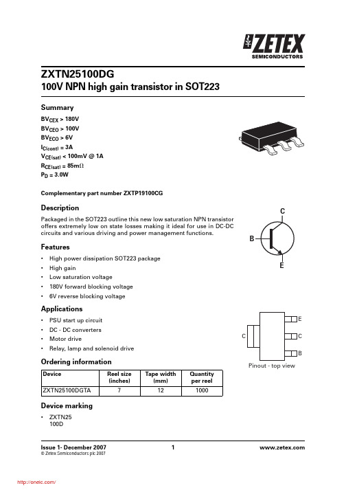
ZXTN25100DG100V NPN high gain transistor in SOT223SummaryBV CEX > 180V BV CEO > 100V BV ECO > 6VI C(cont) = 3A V CE(sat) < 100mV @ 1A R CE(sat) = 85m ⍀P D = 3.0WComplementary part number ZXTP19100CGDescriptionPackaged in the SOT223 outline this new low saturation NPN transistor offers extremely low on state losses making it ideal for use in DC-DC circuits and various driving and power management functions.Features•High power dissipation SOT223 package •High gain•Low saturation voltage •180V forward blocking voltage •6V reverse blocking voltageApplications•PSU start up circuit •DC - DC converters •Motor drive•Relay, lamp and solenoid driveOrdering informationDevice marking•ZXTN25100DDeviceReel size (inches)Tape width(mm)Quantity per reel ZXTN25100DGTA7121000Absolute maximum ratingsThermal resistanceNOTES:(a)For a device surface mounted on 15mm x 15mm x 0.6mm FR4 PCB with high coverage of single sided 1oz copper, in still air conditions.(b)Mounted on 25mm x 25mm x 0.6mm FR4 PCB with high coverage of single sided 1oz copper, in still air conditions.(c)Mmounted on 50mm x 50mm x 0.6mm FR4 PCB with high coverage of single sided 2oz copper, in still air conditions.(d)As (c) above measured at t<5 seconds.(e)Junction to case (collector tab). TypicalParameterSymbol Limit Unit Collector-Base voltageV CBO 180V Collector-Emitter voltage (forward blocking)V CEX 180V Collector-Emitter voltageV CEO 100V Emitter-Collector voltage (reverse blocking)V ECO 6V Emitter-Base voltageV EBO 7V Continuous Collector current (c)I C 3A Base current I B 1A Peak pulse currentI CM 3.5A Power dissipation at T A =25°C (a)Linear derating factorP D1.29.6W mW/°C Power dissipation at T A =25°C (b)Linear derating factorP D 1.612.8W mW/°C Power dissipation at T A =25°C (c)Linear derating factorP D 324W mW/°C Power dissipation at T A =25°C (d)Linear derating factorP D 5.342W mW/°C Power dissipation at T C =25°C (e)Linear derating factorP D 7.358W mW/°C Operating and storage temperature rangeT j , T stg -55 to 150°CParameterSymbol Limit Unit Junction to ambient (a)R ⍜JA 104°C/W Junction to ambient (b)R ⍜JA 78°C/W Junction to ambient (c)R ⍜JA 42°C/W Junction to ambient (d)R ⍜JA 23.5°C/W Junction to case (e)R ⍜JC16°C/WThermal characteristicsElectrical characteristics (at T amb = 25°C unless otherwise stated)ParameterSymbol Min.Typ.Max.Unit Conditions Collector-Base breakdown voltageBV CBO 180220V I C = 100μACollector-Emitter breakdown voltage (forward blocking)BV CEX 180220V I C = 100μA, R BE < 1k Ω or -1V < V BC < 0.25V Collector-Emitter breakdown voltage BV CEO 100130V I C = 10mA (*)NOTES:(*)Measured under pulsed conditions. Pulse width ≤ 300µs; duty cycle ≤ 2%.Emitter-Collector breakdown voltage (reverse blocking)BV ECX 68.2V I E = 100μA, R BC < 1k Ω or 0.25V > V BC > -0.25V Emitter-Collector breakdown voltage (reverse blocking)BV ECO 68.7V I E = 100μA Emitter-Base breakdown voltageBV EBO 78.3V I E = 100μACollector-Base cut-off currentI CBO <1500.5nA μA V CB =180VV CB =180V , T amb =100°C Collector-Emitter cut-off currentI CEX 100nA V CE = 100V, R BE < 1k Ω or -1V < V BE < 0.25V Emitter-Base cut-off currentI EBO <150nA V EB = 5.6VCollector-Emitter saturation voltageV CE(sat)12080215200170100345500mV mV mV mV I C = 0.5A, I B = 10mA (*)I C = 1A, I B = 100mA (*)I C = 2.5A, I B = 250mA (*)I C = 3A, I B = 600mA (*)Base-Emitter saturation voltageV BE(sat)10201100mV I C = 3A, I B = 600mA (*)Base-Emitter turn-on voltageV BE(on)9051000mVI C = 3A, V CE = 2V (*)Static forward current transfer ratioh FE300120404501706010900I C = 10mA, V CE = 2V (*)I C = 0.5A, V CE = 2V (*) I C = 1A, V CE = 2V (*)I C = 3A, V CE = 2V (*)Transition frequency f T 175MHz I C = 50mA, V CE = 10V f = 100MHzInput capacitance C ibo 154250pF V EB = 0.5V, f = 1MHz (*)Output capacitance C obo 8.715pF V CB = 10V, f = 1MHz (*)Delay time t d 16.4ns I C = 500mA, V CC =10V, I B1 = -I B2 = 50mA Rise time t r 115ns Storage time t s 763ns Fall timet f158nsIntentionally left blankPackage outline - SOT223Note: Controlling dimensions are in millimeters. Approximate dimensions are provided in incheslimeters Inches limeters Inches Min.Max.Min.Max.Min.Max.Min.Max.A - 1.80-0.071D 6.306.700.2480.264A10.020.100.00080.004e 2.30 BSC 0.0905 BSC A2 1.55 1.650.06100.0649e1 4.60 BSC 0.181 BSC b 0.660.840.0260.033E 6.707.300.2640.287b2 2.90 3.100.1140.122E1 3.30 3.700.1300.146C0.230.330.0090.013L0.90-0.355-Zetex sales offices EuropeZetex GmbHKustermann-park Balanstraße 59D-81541 München GermanyTelefon: (49) 89 45 49 49 0Fax: (49) 89 45 49 49 49europe.sales@AmericasZetex Inc700 Veterans Memorial Highway Hauppauge, NY 11788USATelephone: (1) 631 360 2222Fax: (1) 631 360 8222usa.sales@Asia PacificZetex (Asia Ltd)3701-04 Metroplaza Tower 1Hing Fong Road, Kwai Fong Hong KongTelephone: (852) 26100 611Fax: (852) 24250 494asia.sales@Corporate HeadquartersZetex Semiconductors plcZetex Technology Park, Chadderton Oldham, OL9 9LL United KingdomTelephone: (44) 161 622 4444Fax: (44) 161 622 4446hq@© 2007 Published by Zetex Semiconductors plcDefinitionsProduct changeZetex Semiconductors reserves the right to alter, without notice, specifications, design, price or conditions of supply of any product or service. Customers are solely responsible for obtaining the latest relevant information before placing orders.Applications disclaimerThe circuits in this design/application note are offered as design ideas. It is the responsibility of the user to ensure that the circuit is fit for the user’s application and meets with the user’s requirements. No representation or warranty is given and no liability whatsoever is assumed by Zetex with respect to the accuracy or use of such information, or infringement of patents or other intellectual property rights arising from such use or otherwise. Zetex does not assume any legal responsibility or will not be held legally liable (whether in contract,tort (including negligence), breach of statutory duty, restriction or otherwise) for any damages, loss of profit, business, contract,opportunity or consequential loss in the use of these circuit applications, under any circumstances.Life supportZetex products are specifically not authorized for use as critical components in life support devices or systems without the express written approval of the Chief Executive Officer of Zetex Semiconductors plc. As used herein:A. Life support devices or systems are devices or systems which:1.are intended to implant into the body or2.support or sustain life and whose failure to perform when properly used in accordance with instructions for use provided in the labeling can be reasonably expected to result in significant injury to the user.B. A critical component is any component in a life support device or system whose failure to perform can be reasonably expected tocause the failure of the life support device or to affect its safety or effectiveness.ReproductionThe product specifications contained in this publication are issued to provide outline information only which (unless agreed by the company in writing) may not be used, applied or reproduced for any purpose or form part of any order or contract or be regarded as a representation relating to the products or services concerned. Terms and ConditionsAll products are sold subjects to Zetex’ terms and conditions of sale, and this disclaimer (save in the event of a conflict between the two when the terms of the contract shall prevail) according to region, supplied at the time of order acknowledgement.For the latest information on technology, delivery terms and conditions and prices, please contact your nearest Zetex sales office.Quality of productZetex is an ISO 9001 and TS16949 certified semiconductor manufacturer.To ensure quality of service and products we strongly advise the purchase of parts directly from Zetex Semiconductors or one of our regionally authorized distributors. For a complete listing of authorized distributors please visit: /salesnetworkZetex Semiconductors does not warrant or accept any liability whatsoever in respect of any parts purchased through unauthorized sales channels.ESD (Electrostatic discharge)Semiconductor devices are susceptible to damage by ESD. Suitable precautions should be taken when handling and transporting devices.The possible damage to devices depends on the circumstances of the handling and transporting, and the nature of the device. The extent of damage can vary from immediate functional or parametric malfunction to degradation of function or performance in use over time.Devices suspected of being affected should be replaced.Green complianceZetex Semiconductors is committed to environmental excellence in all aspects of its operations which includes meeting or exceeding reg-ulatory requirements with respect to the use of hazardous substances. Numerous successful programs have been implemented to reduce the use of hazardous substances and/or emissions.All Zetex components are compliant with the RoHS directive, and through this it is supporting its customers in their compliance with WEEE and ELV directives.Product status key:“Preview”Future device intended for production at some point. Samples may be available “Active”Product status recommended for new designs “Last time buy (LTB)”Device will be discontinued and last time buy period and delivery is in effect “Not recommended for new designs”Device is still in production to support existing designs and production “Obsolete”Production has been discontinued Datasheet status key:“Draft version”This term denotes a very early datasheet version and contains highly provisional information, whichmay change in any manner without notice.“Provisional version”This term denotes a pre-release datasheet. It provides a clear indication of anticipated performance.However, changes to the test conditions and specifications may occur, at any time and without notice.“Issue”This term denotes an issued datasheet containing finalized specifications. However, changes tospecifications may occur, at any time and without notice.分销商库存信息: DIODESZXTN25100DGTA。
MBRB40250TG;中文规格书,Datasheet资料
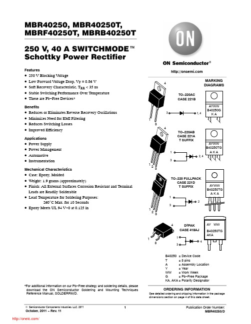
MBR40250, MBR40250T, MBRF40250T, MBRB40250T
TYPICAL CHARACTERISTICS
100
100
IF, MAXIMUM FORWARD CURRENT (A)
TJ = 150°C
TJ = 125°C 10
TJ = 100°C TJ = 25°C
TJ = 150°C
• Power Supply • Power Management • Automotive • Instrumentation
Mechanical Characteristics
• Case: Epoxy, Molded • Weight: 1.9 grams (approximately) • Finish: All External Surfaces Corrosion Resistant and Terminal
AKA
1 3
4
D2PAK
CASE 418AJ
1
4 3
AY WW
B40250TG AKA
*For additional information on our Pb−Free strategy and soldering details, please download the ON Semiconductor Soldering and Mounting Techniques Reference Manual, SOLDERRM/D.
Benefits
• Reduces or Eliminates Reverse Recovery Oscillations • Minimizes Need for EMI Filtering • Reduces Switching Losses • Improved Efficiency
PS2502-2规格书,PS2502-1技术资料,PS2502-4,datasheet,PDF,NEC光耦代理商
Document No. P11303EJ4V0DS00 (4th edition)
The mark shows major revised points.
Date Published September 1997 NS
Printed in Japan
©
1988
深圳市万瑞尔科技有限公司 NEC中国代理商 专营光耦 电话0755-28269789 PS2502-1,-2,-4,PS2502L-1,-2,-4
FORWARD CURRENT vs. FORWARD VOLTAGE
100
50 TA = +100 ˚C +60 ˚C +25 ˚C
10
5
0 ˚C
–25 ˚C
1
–55 ˚C
0.5
0.1 0.7 0.8 0.9 1.0 1.1 1.2 1.3 1.4 1.5 Forward Voltage VF (V)
0.65
0.65
1.25±0.15 2.54
0.50 ± 0.10 0.25 M
0 to 15˚ 1.25±0.15 2.54
0.50 ± 0.10 0.25 M
Caution New package 1-ch only 2
0 to 15˚
深圳市万瑞尔科技有限公司 NEC中国代理商 专营光耦 电话0755-28269789 PS2502-1,-2,-4,PS2502L-1,-2,-4
深圳市万瑞尔科技有限公司nec中国代理商专营光耦wwwwonrealnet电话07552826978911ps2502124ps2502l124memo深圳市万瑞尔科技有限公司nec中国代理商专营光耦wwwwonrealnet电话075528269789ps2502124ps2502l124cautionwithinexistsgaasgalliumarsenidematerialwhichharmfulsubstanceingestedpleasedounderanycircumstancesbreakhermeticseal
ZXTP25020CFHTA;中文规格书,Datasheet资料
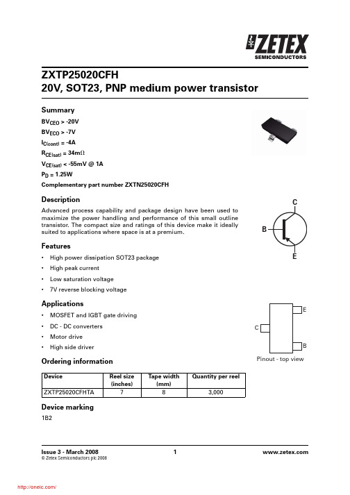
ZXTP25020CFH20V, SOT23, PNP medium power transistorSummaryBV CEO > -20V BV ECO > -7V I C(cont) = -4A R CE(sat) = 34m ⍀V CE(sat) < -55mV @ 1A P D = 1.25WComplementary part number ZXTN25020CFHDescriptionAdvanced process capability and package design have been used to maximize the power handling and performance of this small outline transistor. The compact size and ratings of this device make it ideally suited to applications where space is at a premium.Features•High power dissipation SOT23 package •High peak current •Low saturation voltage •7V reverse blocking voltageApplications•MOSFET and IGBT gate driving •DC - DC converters •Motor drive •High side driverOrdering informationDevice marking1B2DeviceReel size(inches)Tape width(mm)Quantity per reelZXTP25020CFHTA783,000Absolute maximum ratingsParameter Symbol Limit Unit Collector-base voltage V CBO-25V Collector-emitter voltage V CEO-20V Emitter-collector voltage (reverse blocking)V ECO -7V Emitter-base voltage V EBO -7V Continuous collector current(b)I C-4A Peak pulse current I CM-10A Base current I B-1A Power dissipation at T A =25°C(a)P D 0.73W Linear derating factor 5.84mW/°C Power dissipation at T A =25°C(b)P D 1.05W Linear derating factor8.4mW/°C Power dissipation at T A =25°C(c)P D 1.25W Linear derating factor9.6mW/°C Power dissipation at T A =25°C(d)P D 1.81W Linear derating factor14.5mW/°C Operating and storage temperature range T j, T stg -55 to 150°CThermal resistanceParameter Symbol Limit Unit Junction to ambient(a)R⍜JA171°C/W Junction to ambient(b)R⍜JA119°C/W Junction to ambient(c)R⍜JA100°C/W Junction to ambient(d)R⍜JA69°C/W NOTES:(a)For a device surface mounted on 15mm x 15mm x 1.6mm FR4 PCB with high coverage of single sided 1oz copper, instill air conditions.(b)Mounted on 25mm x 25mm x 1.6mm FR4 PCB with a high coverage of single sided 2 oz copper in still air conditions.(c)Mounted on 50mm x 50mm x 1.6mm FR4 PCB with a high coverage of single sided 2 oz copper in still air conditions.(d)As (c) above measured at t<5secs.CharacteristicsElectrical characteristics (at T amb = 25°C unless otherwise stated)ParameterSymbol Min.Typ.Max.Unit Conditions Collector-base breakdown voltageBV CBO -25-50V I C = -100A Collector-emitter breakdown voltage (base open)BV CEO -20-35V I C = -10mA (*) NOTES:(*) Measured under pulsed conditions. Pulse width Յ300s; duty cycle Յ2%.Emitter-base breakdown voltageBV EBO-7-8.2V I E = -100AEmitter-collector breakdown voltage (reverse blocking)BV ECX -7-8.0V I E = -100A (*) R BC < 10k ⍀ or -0.25 < V BC < 0.25V Emitter-collector breakdown voltage (base open)BV ECO -7-8.8V I E = -100A (*)Collector-base cut-off currentI CBO<-1-50-20nA A V CB = -20VV CB = -20V, T amb = 100°C Emitter-base cut-off current I EBO <-1-50nA V EB = -5.6VCollector-emitter saturation voltageV CE(sat)-43-55mV I C = -1A, I B = -100mA (*)-70-100mV I C = -1A, I B = -20mA (*)-120-170mV I C = -2A, I B = -40mA (*)-150-210mV I C = -4A, I B = -200mA (*)Base-emitter saturation voltageV BE(sat)-930-1050mV I C = -4A, I B = -200mA (*)Base-emitter turn-on voltage V BE(on)-810-900mVI C = -4A, V CE = -2V (*)Static forward current transfer ratioh FE200350500I C = -10mA, V CE = -2V (*)150250I C = -1A, V CE = -2V (*)85140I C = -4A, V CE = -2V (*)40I C = -10A, V CE = -2V (*)Transition frequency f T 285MHz I C = -50mA, V CE = -10Vf = 100MHz Output capacitance C OBO 32.440pF V CB = -10V, f = 1MHz (*)Delay time t d 38.4ns V CC = -15V. I C = -750mA, I B1 = I B2= -15mARise time t r 49.2ns Storage time t s 168ns Fall timet f55nsTypical characteristicsIntentionally left blankPackage outline - SOT23Note: Controlling dimensions are in millimeters. Approximate dimensions are provided in inchesDefinitionsProduct changeZetex Semiconductors reserves the right to alter, without notice, specifications, design, price or conditions of supply of any product or service. Customers are solely responsible for obtaining the latest relevant information before placing orders.Applications disclaimerThe circuits in this design/application note are offered as design ideas. It is the responsibility of the user to ensure that the circuit is fit for the user’s application and meets with the user’s requirements. No representation or warranty is given and no liability whatsoever is assumed by Zetex with respect to the accuracy or use of such information, or infringement of patents or other intellectual property rights arising from such use or otherwise. Zetex does not assume any legal responsibility or will not be held legally liable (whether in contract, tort (including negligence), breach of statutory duty, restriction or otherwise) for any damages, loss of profit, business, contract, opportunity or consequential loss in the use of these circuit applications, under any circumstances.Life supportZetex products are specifically not authorized for use as critical components in life support devices or systems without the express written approval of the Chief Executive Officer of Zetex Semiconductors plc. As used herein:A. Life support devices or systems are devices or systems which:1.are intended to implant into the bodyor2.support or sustain life and whose failure to perform when properly used in accordance with instructions for use provided in thelabeling can be reasonably expected to result in significant injury to the user.B. A critical component is any component in a life support device or system whose failure to perform can be reasonably expected tocause the failure of the life support device or to affect its safety or effectiveness.ReproductionThe product specifications contained in this publication are issued to provide outline information only which (unless agreed by the company in writing) may not be used, applied or reproduced for any purpose or form part of any order or contract or be regarded as a representation relating to the products or services concerned.Terms and ConditionsAll products are sold subjects to Zetex’ terms and conditions of sale, and this disclaimer (save in the event of a conflict between the two when the terms of the contract shall prevail) according to region, supplied at the time of order acknowledgement.For the latest information on technology, delivery terms and conditions and prices, please contact your nearest Zetex sales office.Quality of productZetex is an ISO 9001 and TS16949 certified semiconductor manufacturer.To ensure quality of service and products we strongly advise the purchase of parts directly from Zetex Semiconductors or one of our regionally authorized distributors. For a complete listing of authorized distributors please visit: /salesnetworkZetex Semiconductors does not warrant or accept any liability whatsoever in respect of any parts purchased through unauthorized sales channels. ESD(Electrostatic discharge)Semiconductor devices are susceptible to damage by ESD. Suitable precautions should be taken when handling and transporting devices. The possible damage to devices depends on the circumstances of the handling and transporting, and the nature of the device. The extent of damage can vary from immediate functional or parametric malfunction to degradation of function or performance in use over time. Devices suspected of being affected should be replaced.Green complianceZetex Semiconductors is committed to environmental excellence in all aspects of its operations which includes meeting or exceeding reg-ulatory requirements with respect to the use of hazardous substances. Numerous successful programs have been implemented to reduce the use of hazardous substances and/or emissions.All Zetex components are compliant with the RoHS directive, and through this it is supporting its customers in their compliance with WEEE and ELV directives.Product status key:“Preview”Future device intended for production at some point. Samples may be available“Active”Product status recommended for new designs“Last time buy (LTB)”Device will be discontinued and last time buy period and delivery is in effect“Not recommended for new designs”Device is still in production to support existing designs and production“Obsolete”Production has been discontinuedDatasheet status key:“Draft version”This term denotes a very early datasheet version and contains highly provisional information, whichmay change in any manner without notice.“Provisional version”This term denotes a pre-release datasheet. It provides a clear indication of anticipated performance.However, changes to the test conditions and specifications may occur, at any time and without notice.“Issue”This term denotes an issued datasheet containing finalized specifications. However, changes tospecifications may occur, at any time and without notice.Zetex sales officesEuropeZetex GmbH Kustermann-Park Balanstraße 59D-81541 München GermanyTelefon: (49) 89 45 49 49 0 Fax: (49) 89 45 49 49 49 europe.sales@ AmericasZetex Inc700 Veterans Memorial HighwayHauppauge, NY 11788USATelephone: (1) 631 360 2222Fax: (1) 631 360 8222usa.sales@Asia PacificZetex (Asia Ltd)3701-04 Metroplaza Tower 1Hing Fong Road, Kwai FongHong KongTelephone: (852) 26100 611Fax: (852) 24250 494asia.sales@Corporate HeadquartersZetex Semiconductors plcZetex Technology Park, ChaddertonOldham, OL9 9LLUnited KingdomTelephone: (44) 161 622 4444Fax: (44) 161 622 4446hq@© 2008 Published by Zetex Semiconductors plc分销商库存信息: DIODESZXTP25020CFHTA。
ZXTN25020DGTA;中文规格书,Datasheet资料
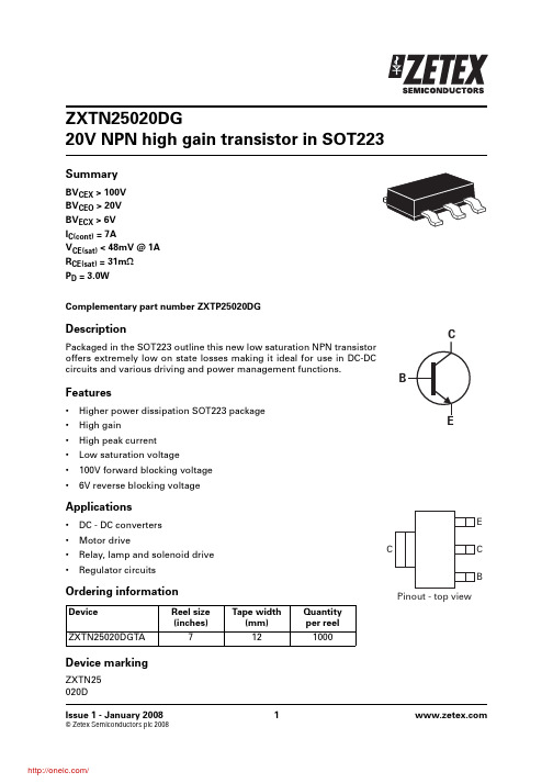
ZXTN25020DG20V NPN high gain transistor in SOT223SummaryBV CEX > 100V BV CEO > 20V BV ECX > 6V I C(cont) = 7AV CE(sat) < 48mV @ 1A R CE(sat) = 31m ΩP D = 3.0WComplementary part number ZXTP25020DGDescriptionPackaged in the SOT223 outline this new low saturation NPN transistor offers extremely low on state losses making it ideal for use in DC-DC circuits and various driving and power management functions.Features•Higher power dissipation SOT223 package •High gain •High peak current •Low saturation voltage •100V forward blocking voltage •6V reverse blocking voltageApplications•DC - DC converters •Motor drive•Relay, lamp and solenoid drive •Regulator circuitsOrdering informationDevice markingZXTN25020DDeviceReel size (inches)Tape width(mm)Quantity per reel ZXTN25020DGTA7121000Absolute maximum ratingsThermal resistanceNOTES:(a)For a device surface mounted on 15mm x 15mm x 0.6mm FR4 PCB with high coverage of single sided 1oz copper, in still air conditions.(b)Mounted on 25mm x 25mm x 0.6mm FR4 PCB with high coverage of single sided 1oz copper, in still air conditions.(c)Mounted on 50mm x 50mm x 0.6mm FR4 PCB with high coverage of single sided 2oz copper, in still air conditions.(d)As (c) above measured at t<5 seconds.(e)Junction to case (collector tab). TypicalParameterSymbol Limit Unit Collector-Base voltageV CBO 100V Collector-Emitter voltage (forward blocking)V CEX 100V Collector-Emitter voltageV CEO 20V Emitter-Collector voltage (reverse blocking)V ECX 6V Emitter-Base voltageV EBO 7V Continuous Collector current (c)I C 7A Base current I B 1A Peak pulse currentI CM 15A Power dissipation at T A =25°C (a)Linear derating factorP D1.29.6W mW/°C Power dissipation at T A =25°C (b)Linear derating factorP D 1.612.8W mW/°C Power dissipation at T A =25°C (c)Linear derating factorP D 3.024W mW/°C Power dissipation at T A =25°C (d)Linear derating factorP D 5.342W mW/°C Power dissipation at T C =25°C (e)Linear derating factorP D 7.358W mW/°C Operating and storage temperature rangeT j , T stg -55 to 150°CParameterSymbol Limit Unit Junction to ambient (a)R ⍜JA 104°C/W Junction to ambient (b)R ⍜JA 78°C/W Junction to ambient (c)R ⍜JA 42°C/W Junction to ambient (d)R ⍜JA 23.5°C/W Junction to case (e)R ⍜JC16°C/WThermal characteristicsElectrical characteristics (at T amb = 25°C unless otherwise stated).Parameter Symbol Min.Typ.Max.Unit Conditions Collector-Base breakdown voltageBV CBO 100125V I C = 100ACollector-Emitter breakdown voltage (forward blocking)BV CEX 100120VI C = 100A, R BE < 1k Ω or-1V < V BE < 0.25V Collector-Emitter breakdown voltage BV CEO 2035V I C = 10mA (*)NOTES:(*)Measured under pulsed conditions. Pulse width ≤ 300µs; duty cycle ≤ 2%.Emitter-Collector breakdown voltage (reverse blocking)BV ECX68.3VI E = 100A, R BC < 1k Ω or0.25V > V BC > -0.25V Emitter-Collector breakdown voltage (reverse blocking)BV ECO 5 6.1VI E = 100A Emitter-Base breakdown voltageBV EBO 78.35V I E = 100ACollector-Base cut-off currentI CBO <1500.5nA A V CB = 100VV CB = 100V, T amb = 100°C Collector-Emitter cut-off currentI CEX100nAV CE = 100V, R BE < 1k Ω or-1V < V BE < 0.25V Emitter cut-off current I EBO <150nA V EB = 5.6VCollector-Emitter saturation voltageV CE(sat)40601001302254875120180290mV mV mV mV mV I C = 1A, I B = 100mA (*)I C = 1A, I B = 20mA (*)I C = 2A, I B = 40mA (*)I C = 2A, I B = 20mA (*)I C = 7A, I B = 700mA (*)Base-Emitter saturation voltageV BE(sat)10901150mV I C = 7A, I B = 700mA (*)Base-Emitter turn-on voltageV BE(on)9501050mVI C = 7A, V CE = 2V (*)Static forward current transfer ratioh FE300250504503608515900I C = 10mA, V CE = 2V (*)I C = 2A, V CE = 2V (*)I C = 7A, V CE = 2V (*)I C = 15A, V CE = 2V (*)Transition frequency f T 215MHz I C = 50mA, V CE = 10V f = 100MHzInput capacitance C ibo 152pFV EB = 0.5V, f = 1MHz (*)Output capacitance C obo 16.525pF V CB = 10V, f = 1MHz (*)Delay time t d 67.7ns I C = 1A, V CC = 10V,I B1 = -I B2 = 10mA Rise time t r 72.2ns Storage time t s 361ns Fall timet f63.9nsZetex sales offices EuropeZetex GmbHKustermann-park Balanstraße 59D-81541 München GermanyTelefon: (49) 89 45 49 49 0Fax: (49) 89 45 49 49 49europe.sales@AmericasZetex Inc700 Veterans Memorial Highway Hauppauge, NY 11788USATelephone: (1) 631 360 2222Fax: (1) 631 360 8222usa.sales@Asia PacificZetex (Asia Ltd)3701-04 Metroplaza Tower 1Hing Fong Road, Kwai Fong Hong KongTelephone: (852) 26100 611Fax: (852) 24250 494asia.sales@Corporate HeadquartersZetex Semiconductors plcZetex Technology Park, Chadderton Oldham, OL9 9LL United KingdomTelephone: (44) 161 622 4444Fax: (44) 161 622 4446hq@© 2008 Published by Zetex Semiconductors plcDefinitionsProduct changeZetex Semiconductors reserves the right to alter, without notice, specifications, design, price or conditions of supply of any product or service. Customers are solely responsible for obtaining the latest relevant information before placing orders.Applications disclaimerThe circuits in this design/application note are offered as design ideas. It is the responsibility of the user to ensure that the circuit is fit for the user’s application and meets with the user’s requirements. No representation or warranty is given and no liability whatsoever is assumed by Zetex with respect to the accuracy or use of such information, or infringement of patents or other intellectual property rights arising from such use or otherwise. Zetex does not assume any legal responsibility or will not be held legally liable (whether in contract,tort (including negligence), breach of statutory duty, restriction or otherwise) for any damages, loss of profit, business, contract,opportunity or consequential loss in the use of these circuit applications, under any circumstances.Life supportZetex products are specifically not authorized for use as critical components in life support devices or systems without the express written approval of the Chief Executive Officer of Zetex Semiconductors plc. As used herein:A. Life support devices or systems are devices or systems which:1.are intended to implant into the body or2.support or sustain life and whose failure to perform when properly used in accordance with instructions for use provided in the labeling can be reasonably expected to result in significant injury to the user.B. A critical component is any component in a life support device or system whose failure to perform can be reasonably expected tocause the failure of the life support device or to affect its safety or effectiveness.ReproductionThe product specifications contained in this publication are issued to provide outline information only which (unless agreed by the company in writing) may not be used, applied or reproduced for any purpose or form part of any order or contract or be regarded as a representation relating to the products or services concerned. Terms and ConditionsAll products are sold subjects to Zetex’ terms and conditions of sale, and this disclaimer (save in the event of a conflict between the two when the terms of the contract shall prevail) according to region, supplied at the time of order acknowledgement.For the latest information on technology, delivery terms and conditions and prices, please contact your nearest Zetex sales office.Quality of productZetex is an ISO 9001 and TS16949 certified semiconductor manufacturer.To ensure quality of service and products we strongly advise the purchase of parts directly from Zetex Semiconductors or one of our regionally authorized distributors. For a complete listing of authorized distributors please visit: /salesnetworkZetex Semiconductors does not warrant or accept any liability whatsoever in respect of any parts purchased through unauthorized sales channels.ESD (Electrostatic discharge)Semiconductor devices are susceptible to damage by ESD. Suitable precautions should be taken when handling and transporting devices.The possible damage to devices depends on the circumstances of the handling and transporting, and the nature of the device. The extent of damage can vary from immediate functional or parametric malfunction to degradation of function or performance in use over time.Devices suspected of being affected should be replaced.Green complianceZetex Semiconductors is committed to environmental excellence in all aspects of its operations which includes meeting or exceeding reg-ulatory requirements with respect to the use of hazardous substances. Numerous successful programs have been implemented to reduce the use of hazardous substances and/or emissions.All Zetex components are compliant with the RoHS directive, and through this it is supporting its customers in their compliance with WEEE and ELV directives.Product status key:“Preview”Future device intended for production at some point. Samples may be available “Active”Product status recommended for new designs “Last time buy (LTB)”Device will be discontinued and last time buy period and delivery is in effect “Not recommended for new designs”Device is still in production to support existing designs and production “Obsolete”Production has been discontinued Datasheet status key:“Draft version”This term denotes a very early datasheet version and contains highly provisional information, whichmay change in any manner without notice.“Provisional version”This term denotes a pre-release datasheet. It provides a clear indication of anticipated performance.However, changes to the test conditions and specifications may occur, at any time and without notice.“Issue”This term denotes an issued datasheet containing finalized specifications. However, changes tospecifications may occur, at any time and without notice.分销商库存信息: DIODESZXTN25020DGTA。
ZXTN25100BFH中文资料(Zetex Semiconductors)中文数据手册「EasyDatasheet - 矽搜」
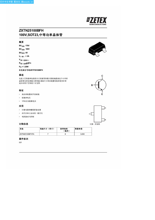
- 100 nA VCE = 136V; R 是
或
-1V V 是
50 nA VEB = 5.6V
40
55 毫伏I =C0,5A,I =50毫B安
(*)
100 135 毫伏I = 0,5A,I =10毫安
(*)
C
B
70
80 毫伏I =C1A,I =百毫B安
(*)
200 250 毫伏I =C3A,I =300B毫安
IC ICM PD
PD
PD
PD
T j, Tstg
限
170 170 100
6 7 3 9 0.73
5.84 1.05
8.4 1.25
9.6 1.81
14.5 - 55到150
热阻
参数
结到环境
(a)
结到环境
(b)
结到环境
(c)
结到环境
(d)
符号
R JA R JA R JA R JA
笔记:
(一)对于器件表面安装在尺寸仅为15mm×尺寸仅为15mm×1.6毫米FR4 PCB覆盖率高单面盎司镀铜,在 静止空气条件.
笔记:
(*)测量脉冲条件下.脉冲宽度
符号
BV CBO
Min. Typ. MAX.单位条件
170 220
V IC = 100 A
BV CEX 170 210
BV CEO 100 120
BV ECX
6
7
BV ECO
6
8.4
IC = 100 A, R 是
或
-1V V 是
V IC = 10mA (*)
V IE = 100 A, R BC 0.25V V BC -0.25V
250V22000uF电容的铝电解电容器
发布日期:2011年6月25日Issued date:DOC12,2011客户名称:Customer:产品规格书Products specification产品种类:铝电解电容器Products types:Aluminum Electrolytic Capacitors产品代码:UGF5AProducts code sigh:产品规格:250V22000μFφ90×170Specification深圳市雅达康电子科技有限公司YDK Technology Ltd.,Shenzhen拟制Designed审核Checked批准Approved刘小姐朱建平一、适用范围Adapt range本产品规格书适用于深圳市雅达康电子科技有限公司250V22000μF铝电解电容器产品。
The products specification is adapted to 250V22000μF Aluminum Electrolytic Capacitors ofYDK Technology Ltd.,Shenzhen二、技术性能Specifications项目Item 特性Performance characteristics使用温度范围(℃)Operation temperature range-40~+105额定电压(V)Rated voltage 250浪涌电压(V)Surge voltage 300标称电容量(μF)Nominal capacitance 22000标称电容量允许偏差(%)Capacitance tolerance±20%漏电流(mA)Leakage current(at 20℃,afer 5minutes)5损耗角正切值(tg δ)Dissipation factor (20℃,120Hz)0.25Ripple current (105℃120Hz)(Arms)56耐久性(105℃)Load life5000小时5000hours三、外形图及尺寸表Case size table(mm )四、纹波电流修正系数ripple current multipliers:频率修正系数Frequency Coefficient 温度修正系数Temperature coefficientφD ±0.7889L ±1.57170F ±0.4131.75频率Freq (Hz)50\601203001K ≥10K 系数factor0.81.001.101.301.40五、试验方法及要求Tests项目Item试验条件Test conditions性能要求Requirements浪涌电压Surge voltage 温度+15~+35℃,施加规定的浪涌电压,充电30秒,放电5分30秒,共循环1000次。
施耐德电气 Symmetra

技术数据 .......................................................................................................8
设备规划 .....................................................................................................22
输入规格 ..................................................................................................22 旁路规格 ..................................................................................................22 输出规格 ..................................................................................................22 电池规格 ..................................................................................................23 带维修旁路的系统概述 ..............................................................................23
T2A10资料
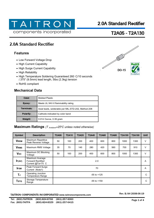
2.0A Standard Rectifier2.0A Standard RectifierFeatures• Low Forward Voltage Drop • High Current Capability• High Surge Current Capability • High Reliability• High Temperature Soldering Guaranteed 260°C/10 seconds /.375" (9.5mm) lead length, 5lbs (2.3kg) tension • RoHS compliantMechanical DataCase: Molded PlasticEpoxy: Meets UL 94V-0 flammability ratingTerminals: Axial leads, solderable per MIL-STD-202, Method 208 Polarity: Cathode indicated by color band Weight:0.014 Ounce, 0.39 gramMaximum Ratings (T Ambient =25ºC unless noted otherwise)SymbolDescription T2A05T2A10T2A20T2A40T2A60T2A80T2A100T2A130UnitV RRM Maximum Repetitive Peak Reverse Voltage 50 100 200 400 600 800 1000 1300 V V RMS Maximum RMS Voltage 3570140280420560700910VV DC Maximum DC Blocking Voltage50 100 200 400 600 800 1000 1300 VI F(AV) Maximum Average Forward Rectified Current @Ta=75° C 2.0 AI FSM Peak Forward Surge Current (Note1) 70 A T J Operating Junction Temperature Range -55 to +125 ° C T STGStorage Temperature Range-55 to +150° CT2A05 - T2A130Ambient Temperature T a (°C) Number of Cycles at 60HzElectrical Characteristics (T Ambient =25ºC unless noted otherwise)Note: 1. 8.3ms single half sine-wave superimposed on rated load (JEDEC method)2. Measured at 1MHz and applied reverse voltage of 4.0Volts D.C.3. Thermal resistance from junction to ambient at .375" (9.5mm) lead length.Typical Characteristics CurvesSymbolDescription T2A05T2A10T2A20T2A40T2A60T2A80T2A100 T2A130UnitV FMaximumForward Voltage @ I F=2.0A 1.0 VT A=25° C 5.0 µA I RMaximum DC Reverse Current at Rated DC Blocking Voltage T A=100° C 50µAC JTypical Junction Capacitance (Note2) 20 pFR θ-JAMaximum Thermal Resistance (Note3)50 °C/WI F (A V ) A v e r a g e F o r w a r d C u rr e n t (A )I F S M I n s t a n t a n e o u s F o r w a r d C u r r e n t (A )Fig.2-Max. Non-Repetitive Forward Surge CurrentFig.1- Forward Current Derating CurveT2A05 - T2A130Fig.4- Typical Reverse CharacteristicsFig.5-Typical Junction CapacitanceReverse Voltage (V)Fig.3-Typical Instantaneous ForwardCharacteristicsV F Instantaneous Forward Voltage (V)I F I n s t a n t a n e o u s F o r w a r d C u r r e n t (A )I R I n s t a n t a n e o u s R e v e r s e C u r r e n t (µA )Percentage of Peak Reverse Voltage (%)C J J u n c t i o n C a p a c i t a n c e (p F )T2A05 - T2A130 Dimensions in inches (mm)DO-15How to contact us:。
ZXTP25100BFH中文资料
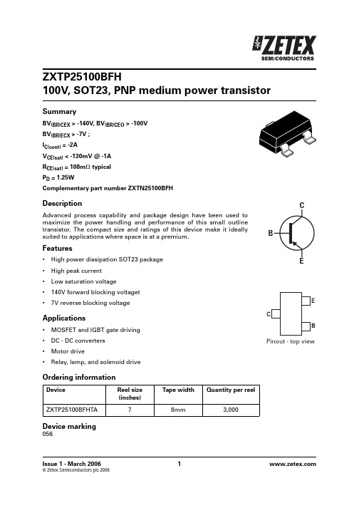
ZXTP25100BFH100V, SOT23, PNP medium power transistorSummaryBV (BR)CEX > -140V, BV (BR)CEO > -100VBV (BR)ECX > -7V ;I C(cont) = -2AV CE(sat) < -130mV @ -1A R CE(sat) = 108m ⍀ typical P D = 1.25WComplementary part number ZXTN25100BFHDescriptionAdvanced process capability and package design have been used to maximize the power handling and performance of this small outline transistor. The compact size and ratings of this device make it ideally suited to applications where space is at a premium.Features•High power dissipation SOT23 package •High peak current •Low saturation voltage •140V forward blocking voltaget •7V reverse blocking voltageApplications•MOSFET and IGBT gate driving •DC - DCconverters•Motor drive•Relay, lamp, and solenoid driveOrdering informationDevice marking056DeviceReel size (inches)Tape widthQuantity per reelZXTP25100BF HTA78mm 3,000Absolute maximum ratingsNOTES:(a)For a device surface mounted on 15mm x 15mm x 1.6mm FR4 PCB with high coverage of single sided 1oz copper, in still air conditions.(b)Mounted on 25mm x 25mm x 1.6mm FR4 PCB with a high coverage of single sided 2 oz copper in still air conditions. (c)Mounted on 50mm x 50mm x 1.6mm FR4 PCB with a high coverage of single sided 2 oz copper in still air conditions. (d)As (c) above measured at t<5secs.ParameterSymbol Limit Unit Collector-base voltageV CBO -140V Collector-emitter voltage (forward blocking)V CEX -140V Collector-emitter voltageV CEO -100V Emitter-collector voltage (reverse blocking)V ECX -7V Emitter-base voltageV EBO -7V Continuous collector current (b)I C -2A Peak pulse currentI CM -5A Power dissipation at T A =25°C (a)Linear derating factorP D 0.735.84W mW/°C Power dissipation at T A =25°C (b)Linear derating factorP D 1.058.4W mW/°C Power dissipation at T A =25°C (c)Linear derating factorP D 1.259.6W mW/°C Power dissipation at T A =25°C (d)Linear derating factorP D 1.8114.5W mW/°C Operating and storage temperature rangeT j , T stg-55 to 150°CThermal resistanceParameterSymbol Limit Unit Junction to ambient (a)R ⍜JA 171°C/W Junction to ambient (b)R ⍜JA 119°C/W Junction to ambient (c)R ⍜JA 100°C/W Junction to ambient (d)R ⍜JA69°C/WCharacteristicsElectrical characteristics (at T AMB = 25°C unless otherwise stated)ParameterSymbolMin.Typ.Max.Unit Conditions Collector-base breakdown voltageBV CBO -140-165V I C = -100A Collector-emitter breakdown voltage (forward blocking)BV CEX-140-165VI C = -100A, R BE < 1k ⍀ or-0.25V < V BE < 1V Collector-emitterbreakdown voltage (base open)BV CEO-100-125VI C = -10mA (*)Emitter-collector breakdown voltage (reverse blocking)BV ECX-78.2VI E = -100A, R BC < 1k ⍀ or-0.25V < V BC < 0.25V Emitter-base breakdown voltageBV EBO -7-8.2V I E = -100ACollector cut-off current I CBO <-1-50-20nA A V CB = -112VV CB = -112V, T AMB = 100°C Collector emitter cut-off currentI CEX--100nAV CE = -112V; R BE < 1k ⍀ or-0.25V < V BE < 1V Emitter cut-off current I EBO <-1-50nA V EB = -5.6VCollector-emitter saturation voltageV CE(sat)-60-90mV I C = -0.5A, I B = -50mA (*)NOTES:(*)Measured under pulsed conditions. Pulse width Յ 300s; duty cycle Յ2%.-240-350mV I C = -0.5A, I B = -10mA (*)-100-130mV I C = -1A, I B = -100mA (*)-215-295mV I C = -2A, I B = -200mA (*)Base-emitter saturation voltageV BE(sat)-900-1000mV I C = -2A, I B = -200mA (*)Base-emitter turn-on voltageV BE(on)-830-950mVI C = -2A, V CE = -2V (*)Static forward current transfer ratioh FE100200300I C = -10mA, V CE = -2V (*)55105I C = -1A, V CE = -2V (*)1525I C = -2A, V CE = -2V (*)Transition frequency f T 200MHzI C = -100mA, V CE = -5V f = 100MHzOutput capacitance C OBO 1525pF V CB = -10V, f = 1MHz (*)Turn-on time t (on)31ns V CC = -10V, I C = -500mA, I B1 = I B2= -50mATurn-off timet (off)384nsTypical characteristicsFor international sales offices visit /officesZetex products are distributed worldwide. For details, see /salesnetworkThis publication is issued to provide outline information only which (unless agreed by the company in writing) may not be used, applied or reproduced for any purpose or form part of any order or contact or be regarded as a representation relating to the products or services concerned.The company reserves the right to alter without notice the specification, design, price or conditions of supply of any product or service.EuropeZetex GmbHStreitfeldstraße 19D-81673 München GermanyTelefon: (49) 89 45 49 49 0Fax: (49) 89 45 49 49 49europe.sales@AmericasZetex Inc700 Veterans Memorial Highway Hauppauge, NY 11788USATelephone: (1) 631 360 2222Fax: (1) 631 360 8222usa.sales@Asia PacificZetex (Asia Ltd)3701-04 Metroplaza Tower 1Hing Fong Road, Kwai Fong Hong KongTelephone: (852) 26100 611Fax: (852) 24250 494asia.sales@Corporate HeadquartersZetex Semiconductors plcZetex Technology Park, Chadderton Oldham, OL9 9LL United KingdomTelephone: (44) 161 622 4444Fax: (44) 161 622 4446hq@Package outline - SOT23Note: Controlling dimensions are in millimeters. Approximate dimensions are provided in incheslimeters Inches limeters Inches Min.Max.Min.Max.Min.Max.Max.Max.A 2.67 3.050.1050.120H 0.330.510.0130.020B 1.20 1.400.0470.055K 0.010.100.00040.004C - 1.10-0.043L 2.10 2.500.0830.0985D 0.370.530.0150.021M 0.450.640.0180.025F 0.0850.150.00340.0059N 0.95 NOM 0.0375 NOMG1.90 NOM 0.075 NOM-----。
A2502系列连接器商品说明书

SpecificationsCurrent rating:3A AC,DC Voltage rating:250V AC,DCTemperature range:-40°C~+105°C Contact resistance:10m ΩMax.Insulation resistance:1000M ΩMin.Withstanding voltage:800V AC/minute *Compliant with RoHS and REACH**Meet the HF/Halogen Free,need to customize**Contact CJT for details*E326732StandardsE326732Ordering Information & DimensionsReference Informations:*Material:Nylon 66,UL94V-0*Suitable CJT A2502-T series Terminal*Mates with CJT A2502WV,WR-XP series Wafer*Color:WhiteReference Informations:*Used in CJT A2502H-XP,A2511H-XP series HousingOrdering information & SpecificationsUnit:mm SEC:A-AOrdering Information:A2502H-XP - *** - ** 1 2 31.Part No.2.Material:(Blank):Nylon 66,UL94V-0GWT:Nylon 66,UL94V-0,GWT 750℃3.Color:(Blank):WhiteRD:Red OR:Orange YL:Yellow GY:Gray BL:Blue PK:Pink BK:Black BR:Brown GN:Green VI:VioletTR:Tomato red LY:Lemon yellow LE:Light blue VY:Vivid yellowReference Informations:*Material:Pin:Brass/Tin over Nickel Insulator:Nylon 66,UL94V-0*Mates with CJT A2502H-XP series Housing *Color:WhiteP.C.B LAYOUTTYPE 2Ordering Information:A2502WV-XP - * - *** - ** - ** 1 2 3 4 51.Part No.2.Style(blank):Type 1 2:Type 23.Material:(Blank):Nylon 66,UL94V-0GWT:Nylon 66,UL94V-0,GWT 750℃4.Color:(Blank):WhiteRD:Red YL:Yellow BL:Blue BK:Black GN:Green 5.Finish:(blank):Tin over Nickel G:Gold over NickelTYPE 1Ordering Information & DimensionsOrdering Information & DimensionsReference Informations:*Material:Pin:Phosphor Bronze/Tin over Nickel Insulator:PBT,UL94V-0*Mates with CJT A2502WVA,WRA-XP,A2502WVB,WRB-XP,A2502WVA-N,WRA-N-XP,A2502WVB-N,WRB-N-XP series Wafer *Color:GrayOrdering Information:A2502HWV-XP - *** - ** 1 2 31.Part No.2.Material:(Blank):PBT,UL94V-0GWT:PBT,UL94V-0,GWT 750℃3.Finish:(blank):Tin over NickelG:Gold over Nickel2P~7P8P~15P16P~20PTYPE 1TYPE 2Reference Informations:*Material:Pin:Brass/Tin over NickelOrdering Information & DimensionsOrdering Information:A2502WR-XP - * - *** - ** - **1 2 3 4 51.Part No.2.Style(blank):Type 12:Type 23.Material:(Blank):Nylon 66,UL94V-0GWT:Nylon 66,UL94V-0,GWT 750℃4.Color:(Blank):WhiteRD:Red OR:OrangeYL:Yellow GY:GrayBL:Blue PK:PinkBK:Black BR:BrownGN:Green VI:VioletTR:Tomato red LY:Lemon yellowLE:Light blue VY:Vivid yellow5.Finish:(blank):Tin over NickelG:Gold over NickelReference Informations:*Material:Pin:Brass/Tin over NickelInsulator:PBT+15%GF,UL94V-0*Mates with CJT A2502HWV-XP series Housing*Color:GrayP.C.B LAYOUT Ordering Information & DimensionsOrdering Information:A2502WVA-XP - *** - **1 2 31.Part No.2.Material:(Blank):PBT,UL94V-0GWT:PBT,UL94V-0,GWT 750℃3.Finish:(blank):Tin over NickelG:Gold over NickelReference Informations:*Material:Pin:Brass/Tin over NickelInsulator:PBT+15%GF,UL94V-0Ordering Information & DimensionsOrdering Information:A2502WRA-XP - *** - ** 1 2 31.Part No.2.Material:(Blank):PBT,UL94V-0GWT:PBT,UL94V-0,GWT 750℃3.Finish:(blank):Tin over Nickel G:Gold over NickelReference Informations:*Material:Pin:Brass/Tin over NickelInsulator:PBT+15%GF,UL94V-0*Mates with CJT A2502HWV-XP series Housing *Color:GrayOrdering Information & DimensionsOrdering Information:A2502WVA-N-XP - *** - ** 1 2 31.Part No.2.Material:(Blank):PBT,UL94V-0GWT:PBT,UL94V-0,GWT 750℃3.Finish:(blank):Tin over Nickel G:Gold over NickelReference Informations:*Material:Pin:Brass/Tin over NickelInsulator:PBT+15%GF,UL94V-0*Mates with CJT A2502HWV-XP series Housing*Color:GrayReference Informations:Ordering Information:Ordering Information:A2502WRA-N-XP - *** - **1 2 31.Part No.2.Material:(Blank):PBT,UL94V-0GWT:PBT,UL94V-0,GWT 750Reference Informations:Reference Informations:Ordering Information:Reference Informations:。
厦门ABBZX2气体绝缘开关设备
厦门ABBZX2气体绝缘开关设备ABBZX2气体绝缘开关设备,是瑞士ABB集团生产的一种高压开关设备。
它采用了先进的气体绝缘技术,具有较小的占地面积、可靠运行、安全性高等特点,广泛应用于发电厂、变电站、装备制造等领域。
设备特点1. 高可靠性ABBZX2气体绝缘开关设备内部采用SF6气体作为绝缘介质,具有优异的绝缘性能,能有效防止漏电、短路等故障发生,维持设备的正常运行。
2. 安全节能ABBZX2气体绝缘开关设备采用先进的气体密封技术,能有效地避免SF6气体泄漏,避免了因SF6气体的温室效应对环境造成的污染。
同时,该设备还具有过载、短路等故障保护功能,能够保证设备的安全运行。
3. 高灵活性ABBZX2气体绝缘开关设备采用了模块化设计,具有结构简单、灵活性强的特点,能够方便地进行组合与拆卸,适用于各种不同场合的应用要求。
4. 低占地面积ABBZX2气体绝缘开关设备结构紧凑、体积小,可以在有限的空间内安装多个设备,大大减少了占地面积,节约了设备安装空间和成本。
技术参数1. 电压等级ABBZX2气体绝缘开关设备的电压等级主要有12kV、24kV和40.5kV三种,可以满足不同场景的应用需求。
2. 额定电流ABBZX2气体绝缘开关设备的额定电流范围为630A-4000A,适用于不同电网的接入需求。
3. 产品系列ABBZX2气体绝缘开关设备有6种不同的产品系列,分别是ZX2-12、ZX2-24、ZX2-40.5、ZX2-12D、ZX2-24D和ZX2-40.5D,覆盖了不同场景的应用需求。
应用范围ABBZX2气体绝缘开关设备已经广泛应用于发电厂、变电站、装备制造等领域,在建筑工程、铁路、工矿企业等重要领域也得到了广泛的应用。
ABBZX2气体绝缘开关设备具有高可靠性、安全节能、高灵活性和低占地面积等诸多优势,是一款极具竞争力的高压开关设备,值得推荐。
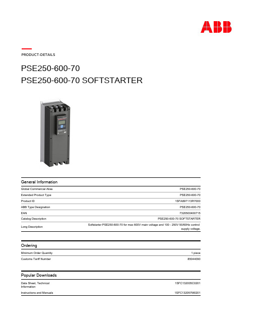
ABB PSE250-600-70 SOFTSTARTER 产品说明书
260 mm 600 mm
310 mm 14.7 kg
7320500400715 1 piece 1 piece
Classifications
Object Classification Code ETIM 4
Q EC002572 - Electronic motor control and protection device
PRODUCT-DETAILS
PSE250-600-70 PSE250-600-70 SOFTSTARTER
General Information
Global Commercial Alias Extended Product Type Product ID ABB Type Designation EAN Catalog Description Long Description
Ordering
Minimum Order Quantity Customs Tariff Number
Popular Downloads
Data Sheet, Technical Information Instructions and Manuals
PSE250-600-70 PSE250-600-70 1SFA897113R7000 PSE250-600-70 7320500400715 PSE250-600-70 SOFTSTARTER Softstarter PSE250-600-70 for max 600V main voltage and 100 - 250V 50/60Hz control supply voltage.
RoHS Status
Storage -40 ... +70 °C Operation -25 ... +60 °C
上海良信NDM3Z-250产品规格书
产品规格书产品名称:塑壳断路器产品型号:NDM3Z-250日期:20141022编制审核批准张颖孙从林李生爱文件名称产品规格书文件编号NDT500536产品型号及名称NDM3Z-250塑壳断路器版次第3版实施日期20141022 修订记录版次修订内容修订日期修订人员0 新增20130924 张颖1 1.去除(DC1000V)J4接线方式、修正通电操作性能:3000次2.新增附件内容20140301 孙从林2 1、增加自由接线产品2、更改海拔高度3、增加相间隔板放置位置20140916 朱乾坤3 增加扭矩值20141022 朱乾坤1、适用范围与用途NDM3Z系列塑料外壳式直流断路器(以下简称断路器),适用于额定工作直流电压1000V及以下,额定工作电流至800A的直流系统中。
断路器具有过载、短路、欠压等保护功能。
能保护线路和电源设备免受过压和过流造成的损坏。
广泛应用于电力发电、输变电、新能源、通讯、建筑等领域。
2、产品图片3级串 4级串3、规格型号说明ND M 3 Z -□□ / □□□□□接线方式(4P)(注1)断路器额定电流(注2)附件代号(见表1)脱扣器形式代号(注3)极数(2、3、4)操作方式(注4)壳架等级电流直流代号设计序号塑料外壳式断路器Nader牌低压电器注1:4P产品接线方式J1、J2、J3、自由接线(见DC1000V接线图),3P产品如需自由接线请备注;注2:额定电流为: 125A、140A、160A、180A、200A、225A、250A;注3:脱扣器形式代号;0:无脱扣器2:仅有瞬时脱扣器3:复式脱扣器表1:附件代号对照表:4、主要技术参数1)电气特性▲额定绝缘电压Ui:1000V额定工作电压Ue:DC500V(两极串) ,DC 750V(三极串), DC 1000V(四极串)▲壳架等级额定电流Inm:250A▲额定极限短路分断电流Icu:DC750V、DC1000V:40 KA,DC500V :35kA▲额定运行短路分断电流Ics:DC750V、DC1000V:25 KA,DC500V: 35kA▲辅助触点额定工作电流: 0.3A▲辅助触点约定发热电流: 3A2)操作性能▲通电:3000次▲不通电:7000次3)接线能力:额定电流 A 125/140 160 180/200/225 250导线截面积 mm250 70 95 1204)辅助触头①辅助触头及其组合②辅助触头接线图③辅助触头电流参数④辅助触头的电寿命⑤辅助触头的接通和分断能力5)报警触头①报警触头及其组合②报警触头接线图断路器正常合分时,触头不动作,只有在自由脱扣(或故障跳闸)后,触头方改变原始状态,及常开变闭合,常闭变打开,待断路器再扣后,触头恢复原来位置。
- 1、下载文档前请自行甄别文档内容的完整性,平台不提供额外的编辑、内容补充、找答案等附加服务。
- 2、"仅部分预览"的文档,不可在线预览部分如存在完整性等问题,可反馈申请退款(可完整预览的文档不适用该条件!)。
- 3、如文档侵犯您的权益,请联系客服反馈,我们会尽快为您处理(人工客服工作时间:9:00-18:30)。
ZXTN25020BFH20V, SOT23, NPN medium power transistorSummaryBV CEX > 50V BV CEO > 20V BV ECO > 3V I C(cont) = 4.5A V CE(sat) < 45 mV @ 1A R CE(sat) = 27 m ⍀P D = 1.25WComplementary part number ZXTP25020BFHDescriptionAdvanced process capability and package design have been used to maximize the power handling and performance of this small outline transistor. The compact size and ratings of this device make it ideally suited to applications where space is at a premium.Features•High power dissipation SOT23 package •High peak current •Low saturation voltage •50V forward blocking voltage •3V reverse blocking voltageApplications•MOSFET gate drivers •Motor control •DC-DC convertersOrdering informationDevice marking1B1DeviceReel size (inches)Tape width (mm)Quantity perreelZXTN25020BFHTA78 3,000Absolute maximum ratingsParameter Symbol Limit Unit Collector-base voltage V CBO50V Collector-emitter voltage (forward blocking)V CEX50V Collector-emitter voltage V CEO20V Emitter-collector voltage (reverse blocking)V ECO3V Emitter-base voltage V EBO7V Continuous collector current(c)I C 4.5A Base current I B1A Peak pulse current I CM10A Power dissipation at T amb =25°C(a)P D0.73W Linear derating factor 5.84mW/°C Power dissipation at T amb =25°C(b)P D 1.05W Linear derating factor8.4mW/°C Power dissipation at T amb =25°C(c)P D 1.25W Linear derating factor9.6mW/°C Power dissipation at T amb =25°C(d)P D 1.81W Linear derating factor14.5mW/°C Operating and storage temperature range T j, T stg- 55 to 150°CThermal graphsParameter Symbol Limit Unit Junction to ambient(a)R⍜JA171°C/W Junction to ambient(b)R⍜JA119°C/W Junction to ambient(c)R⍜JA100°C/W Junction to ambient(d)R⍜JA69°C/W NOTES:(a)For a device surface mounted on 15mm x 15mm x 1.6mm FR4 PCB with high coverage of single sided 1oz copper, instill air conditions.(b)Mounted on 25mm x 25mm x 1.6mm FR4 PCB with a high coverage of single sided 2 oz copper in still air conditions.(c)Mounted on 50mm x 50mm x 1.6mm FR4 PCB with a high coverage of single sided 2 oz copper in still air conditions.(d)As (c) above measured at t<5secs.CharacteristicsElectrical characteristics (at T amb = 25°C unless otherwise stated)ParameterSymbol Min.Typ.Max.Unit Conditions Collector-base breakdown voltageBV CBO 5090V I C = 100ACollector-emitter breakdown voltage (forward blocking)BV CEX 5090I C = 100A, R BE < 1k ⍀ or -1V < V BE < 0.25V Collector-emitter breakdown voltage (base open)BV CEO 2027V I C = 10mA (*) NOTES:(*)Measured under pulsed conditions. Pulse width Յ 300s; duty cycle Յ 2%.Emitter-base breakdown voltageBV EBO 78V I E = 100AEmitter-collector breakdown voltage (reverse blocking)BV ECX 67V I E = 100A, R BC < 1k ⍀ or 0.25V > V BC > -0.25V Emitter-collector breakdown voltage (base open)BV ECO 34.7V I E = 100A,Collector-base cut-off currentI CBO<15020nA A V CB = 40VV CB = 40V, T amb = 100°C Collector-emitter cut-off current I CEX -100nA V CE = 40V; R BE < 1k ⍀ or -1V < V BE < 0.25V Emitter-base cut-off current I EBO <150nAV EB = 5.6VCollector-emitter saturation voltageV CE(sat)3545mV I C = 1A, I B = 100mA (*)5580mV I C = 1A, I B = 20mA (*)90115mV I C = 2A, I B = 40mA (*)175240mV I C = 4.5A, I B = 90mA (*)120145mV I C = 4.5A, I B = 450mA (*)Base-emitter saturation voltage V BE(sat)9101000mV I C = 4.5A, I B = 90mA (*)Base-emitter turn-on voltage V BE(on)825900mV I C = 4.5A, V CE= 2V (*)Static forward current transfer ratioh FE100200300I C = 10mA, V CE = 2V (*)100210I C = 1A, V CE = 2V (*)75160I C = 4.5A, V CE = 2V (*)3070I C = 10A, V CE = 2V (*)Transition frequency f T 185MHz I C = 50mA, V CE = 10V f = 100MHz Output capacitance C OBO 22.730pF V CB = 10V, f = 1MHz (*)Delay time t d 87ns V CC = 10V. I C = 1A,I B1 = I B2= 10mA.Rise time t r 119ns Storage time t s 146ns Fall timet f61nsTypical characteristicsFor international sales offices visit /officesZetex products are distributed worldwide. For details, see /salesnetworkThis publication is issued to provide outline information only which (unless agreed by the company in writing) may not be used, applied or reproduced for any purpose or form part of any order or contact or be regarded as a representation relating to the products or services concerned.The company reserves the right to alter without notice the specification, design, price or conditions of supply of any product or service.EuropeZetex GmbHStreitfeldstraße 19D-81673 München GermanyTelefon: (49) 89 45 49 49 0Fax: (49) 89 45 49 49 49europe.sales@AmericasZetex Inc700 Veterans Memorial Highway Hauppauge, NY 11788USATelephone: (1) 631 360 2222Fax: (1) 631 360 8222usa.sales@Asia PacificZetex (Asia Ltd)3701-04 Metroplaza Tower 1Hing Fong Road, Kwai Fong Hong KongTelephone: (852) 26100 611Fax: (852) 24250 494asia.sales@Corporate HeadquartersZetex Semiconductors plcZetex Technology Park, Chadderton Oldham, OL9 9LL United KingdomTelephone: (44) 161 622 4444Fax: (44) 161 622 4446hq@Package outline - SOT23Note: Controlling dimensions are in millimeters. Approximate dimensions are provided in incheslimeters Inches limeters Inches Min.Max.Min.Max.Min.Max.Max.Max.A 2.67 3.050.1050.120H 0.330.510.0130.020B 1.20 1.400.0470.055K 0.010.100.00040.004C - 1.10-0.043L 2.10 2.500.0830.0985D 0.370.530.0150.021M 0.450.640.0180.025F 0.0850.150.00340.0059N 0.95 NOM 0.0375 NOMG1.90 NOM 0.075 NOM-----分销商库存信息: DIODESZXTN25020BFHTA。
