Fabrication of a hybrid graphenelayered double hydroxide material
石墨烯的制备及其在铅酸电池中的应用
石墨烯的制备及其在铅酸电池中的应用石沫;杨新新;周明明;吴亮;柯娃;李厚训;戴贵平【摘要】添加炭材料能够明显地提高铅酸电池的性能。
石墨烯是具有独特平面二维结构的炭材料,具有很多优异的性能,如良好的导电性和很高的比表面积。
本文综述了石墨烯的制备方法,并对目前石墨烯在铅酸电池中的应用情况进行了研究和总结。
%Carbon materials can significantly improve the performance of lead-acid batteries. Graphene is a kind of carbon materials with unique two-dimensional structure, which has a lot of excellent performance, such as good electrical conductivity and high speciifc surface area. This paper reviews the preparation methods of graphene, and its application in lead-acid batteries.【期刊名称】《蓄电池》【年(卷),期】2015(000)003【总页数】4页(P142-145)【关键词】炭材料;石墨烯;导电性;铅酸电池【作者】石沫;杨新新;周明明;吴亮;柯娃;李厚训;戴贵平【作者单位】超威电源有限公司研究院,浙江湖州313100;超威电源有限公司研究院,浙江湖州313100;超威电源有限公司研究院,浙江湖州313100;超威电源有限公司研究院,浙江湖州313100;超威电源有限公司研究院,浙江湖州313100;超威电源有限公司研究院,浙江湖州313100;超威电源有限公司研究院,浙江湖州313100【正文语种】中文【中图分类】TM912.1石墨烯是碳原子紧密堆积的二维蜂窝状晶格结构的碳质材料,碳原子排列呈平面六边形结构,在二维平面上每个碳原子以 sp2杂化轨道相连接[1]。
石墨烯光电子器件的应用研究进展
石墨烯光电子器件的应用研究进展李绍娟;甘胜;沐浩然;徐庆阳;乔虹;李鹏飞;薛运周;鲍桥梁【摘要】自2004年被发现以来,石墨烯因其卓越的光学和电学性能及其与硅基半导体工艺的兼容性,备受学术界和工业界的广泛关注。
作为一种独特的二维原子晶体薄膜材料,石墨烯有着优异的机械性能、超高的热导率和载流子迁移率、超宽带的光学响应谱及极强的非线性光学特性,使其在新型光学和光电器件领域具有得天独厚的优势。
一系列基于石墨烯的新型光电器件先后被研制出,已显示出优异的性能和良好的应用前景。
此外,近期石墨烯表面等离子体激元的发现及太赫兹器件的研究进一步促进了石墨烯基光电器件的蓬勃发展。
综述重点总结近年来石墨烯在超快脉冲激光器、光调制器、光探测器以及表面等离子体领域的应用研究进展,并进一步分析目前所面临的主要问题、挑战及其发展趋势。
%Graphene has very significant optical and electronic properties, which attract enormous attention. As a unique two-di-mensional crystal with one atom thickness, it has high electron and thermal conductivities in addition to ? exibility, robustness and impermeability to gases. Its ultra-broad band optical response and excellent non-linear optical properties make it a wonderful material for developing next generation photonic and optoelectronic devices. The fabrication of graphene-based devices is compatible with the existing semiconductor process, which has stimulated lots of graphene-based hybrid silicon-CMOS ( Complementary metal-oxide-semiconductor transistor) applications. Here we review the latest progress in graphene-based photonic and optoelectronic devices, ranging from pulsed lasers, modulators and photodetectors to optical sensors. Other exciting topicssuch as graphene surface plas-mons and their terahertz applications are also discussed.【期刊名称】《新型炭材料》【年(卷),期】2014(000)005【总页数】28页(P329-356)【关键词】石墨烯;脉冲激光器;光调制器;光探测器;表面等离子体;太赫兹【作者】李绍娟;甘胜;沐浩然;徐庆阳;乔虹;李鹏飞;薛运周;鲍桥梁【作者单位】苏州大学功能纳米与软物质研究院,苏州纳米科技协同创新中心,江苏省碳基功能材料与器件高技术研究重点实验室,江苏苏州 215123;苏州大学功能纳米与软物质研究院,苏州纳米科技协同创新中心,江苏省碳基功能材料与器件高技术研究重点实验室,江苏苏州 215123;苏州大学功能纳米与软物质研究院,苏州纳米科技协同创新中心,江苏省碳基功能材料与器件高技术研究重点实验室,江苏苏州 215123;苏州大学功能纳米与软物质研究院,苏州纳米科技协同创新中心,江苏省碳基功能材料与器件高技术研究重点实验室,江苏苏州 215123;苏州大学功能纳米与软物质研究院,苏州纳米科技协同创新中心,江苏省碳基功能材料与器件高技术研究重点实验室,江苏苏州 215123;苏州大学功能纳米与软物质研究院,苏州纳米科技协同创新中心,江苏省碳基功能材料与器件高技术研究重点实验室,江苏苏州 215123;苏州大学功能纳米与软物质研究院,苏州纳米科技协同创新中心,江苏省碳基功能材料与器件高技术研究重点实验室,江苏苏州215123;苏州大学功能纳米与软物质研究院,苏州纳米科技协同创新中心,江苏省碳基功能材料与器件高技术研究重点实验室,江苏苏州 215123【正文语种】中文【中图分类】TM9101 前言硅基光电子技术曾被寄希望于能够实现未来的超高速宽带数据通讯,然而,由于硅基器件目前面临着难以进一步微型化、集约化等问题,从而阻碍了其在高速、宽带数据计算和传输领域的应用。
物理学科常用单词
ensemble报错英[ɒn'sɒmb(ə)l]美[ɑn'sɑmbl]跟读口语练习∙n. 全体;总效果;全套服装;全套家具;合奏组∙adv. 同时∙oxide-assistant growth氧化物辅助生长penetration[pen·e·tra·tion || ‚penɪ'treɪʃn]n.穿透; 穿透深度; 穿透能力; 渗透electrode[e·lec·trode || ɪ'lektrəʊd]n.电极weak[wɪːk]adj.不牢固的, 虚弱的, 弱的trivial[ˈtriviəl]a.琐碎的,不重要的type[taɪp]n.类型, 模范, 典型hybrid['haibrid]n.混血儿, 杂种, 混合物a.混合的, 杂种的, 混合语的potential barrier penetration 势垒贯穿linear harmonic oscillator 线性谐振子zero proint energy 零点能Coulomb field 库仑场operator 算符angular momentum operator 角动量算符eigen value 本征值secular equation 久期方程dipole transition 偶极子跃迁filter[fil·ter || 'fɪltə(r)]n.过滤器, 用于分隔过滤的东西;v.过滤, 走漏, 渗透; 滤过; 走漏; 渗入thermionic[,θә:mi'ɒnik]a.热离子的[电]热离energy barrier2能障(能量位垒)trade off物物交换, 交换; 权衡, 让步parameter[pa·ram·e·ter || pə'ræmɪtə(r)]n.参数, 参量; 界限; 因素, 特征;external[ex'ter·nal || -nl]n.外部; 外面adj.外部的, 表面的, 客观的finite[fi·nite || 'faɪnaɪt]adj.有限的; 限定的; 有穷的an idealized quantum wirecomplementaryadj.补充的; 补足的seebeck coefficient[电]塞贝克系数generic[ge·ner·ic || dʒɪ'nerɪk]adj.属的; 一般的; 类的tuning[tun·ing || 'tuːnɪŋ/'tju-]n.调音, 调律, 调整coefficient[co·ef·fi·cient || ‚kəʊɪ'fɪʃnt]n.系数power factor[化]功率因数evaluate[e·val·u·ate || ɪ'væljʊeɪt]v.评估, 赋值, 评价open circuit[化]开路; 断路[医]断路, 切断电路operatinga.操作的, 工作的, 营业上的, 业务的, 关于收支的, 关于损益的, 外科手术的approach[əˈprəutʃ]v.靠近n.接近,临近;途径;方式,方法chemical potential化学势mechanism[mech·a·nism || 'mekənɪzm]n.机械, 结构, 机构be independent of temperature.compare our results across the three systems configuration[con·fig·u·ra·tion || kən‚fɪgjʊ'reɪʃn] n.结构; 形态; 表面配置; 行星的方位for simplicity为简单起见symmetrically[si'metikli]ad.匀称地, 对称地equilibrium[,i:kwi'libriәm]n.平衡, 平静, 均衡[化]平衡[医]平衡at equilibriumnonlinear operationnonlinear[ˈnɔnˈliniə]非线性; 非线性的; 非直线型的非线性运算division[di·vi·sion || dɪ'vɪʒn]n.区分, 分开, 除法; 部门magnetotransport磁运输measurement['meas·ure·ment || 'meʒə(r)mənt] n.测量法; 尺寸; 度量presence[pres·ence || 'prezns]n.出席, 存在, 到场the orbital motion of electrons电子轨道运动preserveda.喝醉的[计]保留的spin-orbit interaction[化]自旋轨道偶合interaction[ˌintəˈrækʃən]n.相互作用,相互影响fluctuation[fluc·tu·a·tion || ‚flʌktʃʊ'eɪʃn]n.波动; 动摇; 变动deduce[diˈdju:s]vt.推论,推断,演绎ground state基态first excited statea fixed number of electronspromising['prom·is·ing || 'prɑmɪsɪŋ/'prɒm-] adj.有希望的, 前途有望的spintronics自旋电子学effective mass[电]有效质量magnetic moment[化]磁矩concerning[con'cerning || -nɪŋ]prep.关于spin[spin]n.旋转, 自旋, 疾驰, 情绪低落fabrication[fab·ri·ca·tion || ‚fæbrɪ'keɪʃn] n.制作; 伪造物; 构成fabrication[fab·ri·ca·tion || ‚fæbrɪ'keɪʃn] n.制作; 伪造物; 构成epitaxial[ˏepɪˋtæksɪəl]外延的render[ˈrendə]vt.使得,致使;给予,提供;翻译magnetic field磁场spectrum[spec·trum || 'spektrəm]n.谱; 频谱; 光谱; 射频频谱the quenching of the orbital momentum轨道动量的淬灭quantum devices量子器件nanomaterialparticle[par·ti·cle || 'pɑrtɪkl /'pɑːt-]n.粒子, 极小量, 点A strongreduction in the effective electron or hole g factor toward 2 ultra[ul·tra || 'ʌltrə]adj.过度的, 极端的, 过激的heterostructure[ˏhetərəʊˋstrʌktʃə(r)]异晶结构; 异质结构exceed[ex·ceed || ɪk'siːd]v.超过, 胜过, 超越magnetic field splitting磁场劈裂complementaryadj.补充的; 补足的blockade[block·ade || blɒ'keɪd]n.封锁; 障碍物, 阻碍物; 道路阻塞v.封锁; 挡住; 阻塞chargestabilitydiagram电荷稳定性图conductance ridges电导脊fabricate['fab·ri·cate || 'fæbrɪkeɪt]v.制造; 伪造; 组装; 杜撰reactor[riˈæktə]n.反应堆aerosol['єәrәusɒl]n.烟, 雾[化]气溶胶; 烟雾剂diameter[di·am·e·ter || daɪ'æmɪtə]n.直径substraten.底层, 地层, 衬底, 基底, 基质, 酶作用物, 酶解物[计]衬底; 基片[化]反应物nucleation[化]成核作用with respect to关于,至于indiumn.铟antimony[an·ti·mo·ny || 'æntɪmənɪ]n.锑blende[blend]n.闪锌矿stacking faults,twin boundarieswithatomically flat {110}doped[dəupt]掺杂的; 掺杂过的thick[θɪk]adj.厚的, 浓的, 粗壮的adv.厚厚地; 浓浓地; 密集地; 强烈地capping layer覆盖层lithography[li'θɒgrәfi]n.平版印刷术electron beam.电子束etch[etʃ]v.蚀刻, 蚀镂; 施行蚀刻法solution[so·lu·tion || sə'luːʃn]n.解决, 溶液, 解答evaporation[e·vap·o·ra·tion || ɪ‚væpə'reɪʃn]n.蒸发; 消失; 发散rinse[rɪns]n.冲洗; 染发; 漂洗; 染发剂v.以清水冲洗, 漂清, 漱arebriefly etched in a (NH4)2S x solution followed by a rinse inH2Ofabricate['fab·ri·cate || 'fæbrɪkeɪt]v.制造; 伪造; 组装; 杜撰probe[prəʊb]n.探针, 探测针, 调查v.用探针测, 详细调查; 用探针探查, 探测; 调查; 查究probe station探针台cryostat['kraiәstæt]n.低温恒温器versus[ˈvə:səs]prep.以…为对手,对;与…相比之下source-drain voltageback gate voltage, V bgcontact separation[电]接触分离diamond-shaped[ˋdaɪəməndˋʃeɪpt]菱形even['i:vәn]a.平坦的, 相等的, 连贯的, 均等的, 公平的, 偶数的, 平均的, 平衡的, 恰好的vt.使平坦, 使相等vi.变平, 成为相等ad.甚至, 实际上, 完全, 十分odd[ɑd /ɒd]adj.奇数的, 剩余的, 古怪的alternate['ɒ:ltәnәt]a.交替的, 轮流的, 间隔的vt.轮流, (使)交替vi.轮流, (使)交替alternating交替的; 更迭的spin degeneracy[化]自旋简并性degeneracy[diˈdʒenərəsi]蜕化; 退化; 简并度; 简并性lateral[lat·er·al || 'lætərəl]n.侧部; 边音; 支线adj.侧面的, 旁边的oscillation[os·cil·la·tion || ɑsɪ'leɪʃn /ɒs-] n.摆动; 振动评击]wurtzite[ˈwəːtsait]纤维锌矿; 纤锌矿in thewurtzite phase,in the zinc blende phasedetachment[diˈtætʃmənt]after detachment from the growthsubstratequantized量子化的topological拓扑的helical[ˈhelikəl]螺线; 螺旋; 螺旋形plateau[ˈplætəu]n.高原;(上升后的)稳定时期(或状态)subband次能带spin−orbit coupling自选轨道耦合in the presence of a strong spin−orbit coupling由于一个强的自旋轨道耦合quasi['kwɑ:zi:]a.类似的, 准的computation[com·pu·ta·tion || ‚kɒmpjuː'teɪʃn]n.计算, 计量, 计数platform[plat·form || 'plætfɔrm /-fɔːm]n.月台, 坛, 讲台polarization[po·lar·i·za·tion || ‚pəʊləraɪ'zeɪʃn]n.产生极性; 偏振; 极化; 对立, 给予两个相反的倾向;hybrid[ˈhaibrid]桥接; 桥接岔路; 杂化; 杂种; 间生; 混合; 混合; 混合物; 混频环; 混杂的fulfillment[ful'fill·ment || fʊl'fɪlmənt]n.完成, 履行; 满足, 成就; 实现extent[ikˈstent]n.程度,范围,限度;广度,宽度,大小signature['signәtʃә]n.签字, 识别标志, 调号diffusive[di'fju:siv]a.散播的, 冗长的, 扩散的The formation of subbandsspin-degenerate自旋简并suppression[sup'pres·sion || sə'preʃn]n.压制; 禁止; 镇压; 抑制micrometer[mai'krɒmitә]n.测微计[医]微米imperfection[im·per·fec·tion || ‚ɪmpə(r)'fekʃn]n.不完美; 瑕疵; 缺点scatteringn.分散; 散落backscattering[ˋbækˏskætərɪŋ]geometry[ge'om·e·try || dʒɪ'ɑmɪtrɪ/-'ɒm-]n.几何学constriction[kәn'strikʃәn]n.压缩, 收缩, 紧压的感觉trajectory[trəˈdʒektəri]n.(抛射物)弹道轨道indication[in·di·ca·tion || ‚ɪndɪ'keɪʃn]n.指出; 迹象; 指示quasi['kwɑ:zi:]a.类似的, 准的spectroscopy[spek'trɒskәpi]n.光谱学lock(-)in同步intermediate[,in·ter'me·di·ate || ‚ɪntə(r)'mɪːdɪeɪtd] n.中间物, 调停者v.作中间人; 干预adj.中间的, 中级的fraction[frac·tion || 'frækʃn]n.分数, 破片, 小部分confirmation[con·fir·ma·tion || ‚kɒnfə'meɪʃn]n.证实, 批准, 巩固; 确认derivative[diˈrivətiv]变型; 导数; 从变量; 派生的; 派生物; 衍化物; 衍生物; 诱导剂The derivative of conductance to gate voltage电导对于栅电压的导数transconductance[计]跨导intersect[ˌintəˈsekt ; -ər-]交叉; 相交schematicallyadv.纲要性地; 图表式地pronounced[pro'nounced || prə'naʊnst]adj.显著的, 明白的, 断然的dominate['domi·nate || 'dɑmɪneɪt /'dɒm]v.支配, 控制, 统治; 高耸于dominated中等的; 中等木obscure[əbˈskjuə]a.不著名的;费解的vt.使变模糊,掩盖enabling observation of the 0.5g Qplateau for B ≥2 T and the 1.0g Q plateau for B ≥3 T.schematic[sche·mat·ic || skɪː'mætɪk]adj.概要的, 图解的macroscopic英[,mækrə(ʊ)'skɒpɪk]美[,mækrə'skɑpɪk]adj. 宏观的;肉眼可见的coherent transport line for microscopic quantum system 微观量子系统的相干输运过程intersection英[ɪntə'sekʃ(ə)n]美[,ɪntɚ'sɛkʃən]∙n. 交叉;十字路口;交集;交叉点The schematic of Ohm’s law of classical transport for macroscopic system 对于宏观系统经典输运欧姆定律的图解discharge英[dɪs'tʃɑːdʒ]美[dɪs'tʃɑrdʒ]∙vt. 解雇;卸下;放出;免除∙vi. 排放;卸货;流出∙n. 排放;卸货;解雇放电the microstructure evolution of silicon nanowires during the charge/discharge process as severing for the anodematerialforlithium-ion batteries;thecharge-dischargecharacteristic curves.充放电特征曲线锂电池充放电过程中硅纳米线作为阳极的演化规律anode英['ænəʊd]美['ænod]∙n. [电子] 阳极,[电] 正极。
纤维素模板法制备多孔碳纳米棒及其超级电容器性能(英文)
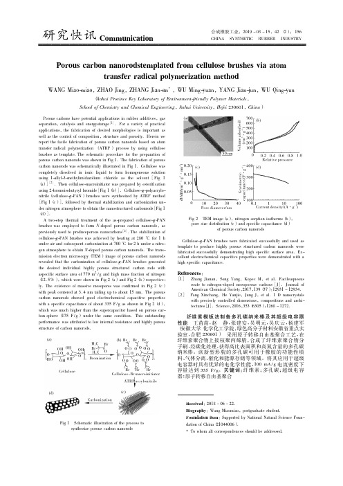
Porous carbons have potential applications in rubber additives,gas separation,catalysis and energystorage[1]. For a variety of practical applications,the fabrication of desired morphologies is important as well as the control of composition,structure and porosity. Herein we report the facile fabrication of porous carbon nanorods based on atom transfer radical polymerization ( ATRP ) process by using cellulose brushes as template. The schematic procedure for the preparation of porous carbon nanorods was shown in Fig 1. The fabrication of porous carbon nanorods was schematically illustrated in Fig 1. Cellulose was completely dissolved in ionic liquid to form homogeneous solution using 1-allyl-3-methylimidazolium chloride as the solvent [Fig 1 ( a) ][2]. Then cellulose-macroinitiator was prepared by esterification using 2-bromoisobutyryl bromide[Fig 1( b) ]. Cellulose-g-polyacrylonitrile( cellulose-g-PAN) brushes were synthesized by ATRP method [Fig 1( c) ],followed by thermal stabilization and carbonization under nitrogen atmosphere to obtain the nanostructured carbonrods[Fig 1 ( d) ].
细胞与材料存在多种相互作用关系
Ⅰ Materials as Protector
Gelatin was used to mimic the Extracellular Matrix (ECM) that provided a biocompatible environment for encapsulated cells
FIG.2 GB & Preparation scheme of cationic gelatin (GA).
The sucrose solution, which was 37 μm in diameter in air, spread out once it landed on the glass surface to a final diameter of 250 μm.
FIG.7 3T3 fibroblasts printed in 8.5% sucrose, 0.3% dextrose in DI water on a glass substrate. White field and fluorescent image (cell tracker die) as well as the overlap of these two images demonstrated that the captured entity is a cell
The focused beam causes the thermal and/or photomechanical volatilization of a small amount of solution near the interface, resulting in ejection of a small number of cells.
Ⅰ Laser assisted bioprinting of human osteosarcoma cells
石墨烯气凝胶保温材料

石墨烯气凝胶保温材料英文回答:Graphene aerogel is a highly efficient and lightweight insulating material that has gained significant attentionin recent years. As a three-dimensional network of graphene sheets, it possesses remarkable properties such as low density, high porosity, and excellent thermal conductivity. These unique characteristics make it an ideal candidate for various applications in the field of thermal insulation.One of the key advantages of graphene aerogel as a thermal insulation material is its exceptional thermal conductivity. Due to its highly porous structure, it can effectively trap and slow down the transfer of heat. This property enables it to provide excellent insulation and reduce heat loss. For example, when used as insulation in buildings, graphene aerogel can significantly improve energy efficiency by reducing the need for heating and cooling.Furthermore, graphene aerogel is also highly flexible and compressible, making it suitable for use in various forms and shapes. It can be easily molded into different structures, such as sheets, films, or even coatings, to fit specific applications. This versatility allows for its integration into existing insulation systems without major modifications.In addition to its thermal insulation properties, graphene aerogel also exhibits excellent mechanicalstrength and stability. It can withstand high temperatures and maintain its structural integrity, even under extreme conditions. This durability makes it a reliable and long-lasting insulation material.Moreover, graphene aerogel is environmentally friendly and sustainable. It is derived from graphene, which is a carbon-based material, and can be produced from renewable sources. Unlike traditional insulation materials, it does not release harmful gases or chemicals into the environment. This aspect aligns with the growing demand for eco-friendlysolutions in various industries.中文回答:石墨烯气凝胶是一种高效轻便的保温材料,在近年来引起了广泛的关注。
“Graphene”研究及翻译

“Graphene”研究及翻译摘要:查阅近5年我国SCI、EI期源刊有关石墨烯研究873篇,石墨烯研究的有关翻译存在很大差异。
从石墨烯的发现史及简介,谈石墨烯内涵及研究的相关翻译。
指出“石墨烯”有关术语翻译、英文题目、摘要撰写应注意的问题。
关键词:石墨烯;石墨烯术语;翻译石墨烯是目前发现的唯一存在的二维自由态原子晶体,它是构筑零维富勒烯、一维碳纳米管、三维体相石墨等sp2杂化碳的基本结构单元,具有很多奇异的电子及机械性能。
因而吸引了化学、材料等其他领域科学家的高度关注。
近5年我国SCI、EI期源刊研究论文873篇,论文质量良莠不齐,发表的论文有35.97%尚未被引用过,占国际论文被引的4.84%左右。
石墨烯研究的有关翻译也存在很大差异。
为了更好的进行国际学术交流,规范化专业术语。
本文就“graphene”的内涵及翻译谈以下看法。
l “Graphene”的发现史及简介1962年,Boehm等人在电镜上观察到了数层甚至单层石墨(氧化物)的存在,1975年van Bom-mel等人报道少层石墨片的外延生长研究,1999年德克萨斯大学奥斯汀分校的R Ruoff等人对用透明胶带从块体石墨剥离薄层石墨片的尝试进行相关报道。
2004年曼彻斯特大学的Novoselov和Geim小组以石墨为原料,通过微机械力剥离法得到一系列叫作二维原子晶体的新材料——石墨烯,并于10月22日在Sclence期刊上发表有关少层乃至单层石墨片的独特电学性质的文章,2010年Gelm和No-voselov获得了诺贝尔物理学奖。
石墨烯有着巨大的比表面积(2630 m2/g)、极高的杨氏模量(1.06 TPa)和断裂应力(~130GPa)、超高电导率(~106 S/cm)和热导率(5000W/m·K)。
石墨烯中的载流子迁移率远高于传统的硅材料,室温下载流子的本征迁移率高达200000 cm2/V.s),而典型的硅场效应晶体管的电子迁移率仅约1000 cm2/V.s。
一种噻吩基双偶极半菁与普鲁士蓝的静电自组装薄膜
一种噻吩基双偶极半菁与普鲁士蓝的静电自组装薄膜王志平;罗虹;高丽华;王科志【摘要】We successfully prepared a novel inorganic-organic hybrid electrostatically self-assembled multilayer film by alternately depositing Prussian blue (PB) and a thiophene-containing hemicyanine. The optical, electrochemical, and photoelectrochemical properties of the as-prepared films were studied by UV-visible absorption spectroscopy, cyclic voltammetry, and photoelectrochemical experiment. Linear increases in the absorbances at 376 and 698 nm with the number of deposited layers, up to at least 8 layers, indicated that film deposition was uniform and reproducible. The PB in the prepared films was found to occur surface-confined rather than diffusion-controlled redox reactions and the peak currents increased with an increase in the number of layers up to 5 layers. Upon irradiation with 100 mW· cm-2 white light the films exhibited stable and reproducible cathodic photocurrents, which increased as the number of layers increased up to 4 layers. A maximum photocurrent density of 0.28 μA· cm-2 was found for the four-layer film at a bias voltage of -0.4 V vs the saturated calomel electrode.%通过交替沉积普鲁士蓝和一种含噻吩的半菁,制备了一种新的无机-有机杂化静电自组装膜.用紫外-可见吸收光谱、循环伏安技术和光电化学实验对薄膜进行了表征或光电性质研究.376和698 nm处薄膜的吸光度随薄膜层数增加线性增加,表明薄膜的沉积是均匀和可重复的.薄膜中的普鲁士蓝具有良好的表面控制而非扩散控制的电化学活性.膜的层数从1增加至5时,阳极峰电流随膜层数增加而线性增加.100 mW·cm-2的白光照射下,薄膜产生稳定的阴极光电流,随层数增加线性增长,层数增加到4层时,光电流达到最大值.饱和甘汞电极为参比电极,-0.4 V偏压下,4层薄膜产生的光电流密度高达0.28 μA·cm-2.【期刊名称】《物理化学学报》【年(卷),期】2011(027)003【总页数】5页(P754-758)【关键词】半菁;自组装膜;循环伏安;紫外可见光谱;噻吩;光电化学性质【作者】王志平;罗虹;高丽华;王科志【作者单位】北京师范大学化学学院,北京100875;集宁师范学院,内蒙古集宁012000;北京师范大学化学学院,北京100875;北京工商大学化学与环境工程学院,北京100048;北京师范大学化学学院,北京100875【正文语种】中文【中图分类】O646Abstract: We successfully prepared a novel inorganic-organic hybrid electrostatically self-assembled multilayer film by alternately depositing Prussian blue(PB)and a thiophene-containing hemicyanine.Theoptical,electrochemical,and photoelectrochemical properties of the as-prepared films were studied by UV-visible absorption spectroscopy,cyclic voltammetry,and photoelectrochemical experiment.Linear increases in the absorbances at 376 and 698 nm with the number of deposited layers,up to at least 8 layers,indicated that film deposition was uniform and reproducible.The PB in the prepared films was found to occur surface-confined rather than diffusion-controlled redox reactions and the peak currents increased with an increase in the number of layers up to 5 layers.Upon irradiation with 100 mW·cm-2white light the films exhibited stable and reproducible cathodic photocurrents,which increased as the number of layers increased up to 4 layers.A maximum photocurrent density of 0.28 μA·cm-2was found for the four-layer film at a bias voltage of-0.4 Vvsthe saturated calomel electrode.Key Words:Hemicyanine;Self-assembled film;Cyclic voltammetry;UV-visible spectrum;Thiophene;Photoelectrochemical propertyDecher1发展的以静电作用力为驱动、将阴阳离子交替沉积吸附制备自组装膜的技术,由于具有方法简单、厚度可控、性质稳定和高度的分子水平组装能力的特点,已引起科学工作者的广泛关注,而有机-无机杂化材料的静电自组装膜已成为目前研究的热点.2,3半菁化合物是备受关注的二阶非线性光学和光电转换材料,过去的十几年的时间里主要采用Langmuir-Blodgett(LB)技术制备多层薄膜,4-10但LB技术具有仪器昂贵、制备费时和薄膜不够稳定等缺点.近年我们曾报道了双偶极半菁和Ru(II)配合物与杂多/同多阴离子、普鲁士蓝和WO3形成的静电自组装多层薄膜,表现出诱人的二阶非线性光学性质和光电转换性质.11-19噻吩是重要的导电聚合物单体,在发光二极管、太阳能电池和场效应晶体管领域有重要应用前景.20普鲁士蓝是一类重要的电致变色、传感和磁学材料.21-24但含噻吩的半菁静电自组装膜未见文献报道.本文报道一种含噻吩基的新双偶极半菁衍生物与普鲁士蓝形成的静电自组装膜以及薄膜的氧化还原和光电化学性质,旨在为这种原料易得、制备简单的有机-无机复合的纳米薄膜材料在多领域的应用提供重要的基础实验数据.用于成膜的含噻吩基双偶极半菁(分子结构示于图1,简记为ABr2),按文献5,11报道的方法合成,经元素分析和核磁共振谱表征.普鲁士蓝{KFeIII4[FeII(CN)6]3}(简记为KFeIII-FeII)按文献14报道的方法合成.GBC Cintra 10e型紫外-可见分光光度计(澳大利亚);pHS3酸度计(上海精密科学仪器有限公司);CHI420电化学分析仪(上海辰华仪器公司);采用三电极系统,覆盖有自组装膜的氧化铟-氧化锡(ITO)玻璃为工作电极,铂丝为对电极,饱和甘汞电极为参比电极,支持电解质为0.5 mol·L-1的Na2SO4溶液(pH=1.93).白光光源(光强为100 mW·cm-2)为配有红外和紫外截止滤光片的500 W高压氙灯光源系统(北京畅拓科技有限公司),薄膜光照的有效面积为0.28 cm2.将石英和玻璃基片分别用98%浓硫酸:30%双氧水(体积比为3:1)和25%氨水:30%双氧水:水(体积比为1:1:5)清洁和亲水处理;ITO玻璃用氢氧化钠的饱和乙醇溶液清洁和亲水处理.处理后的石英和ITO基片按图2所示的途径途组装薄膜.首先按文献3,7,8方法进行表面硅烷化和氨基质子化,然后依次分别浸入1.0 mmol·L-1普鲁士蓝水溶液30 min和1.0 mmol·L-1ABr2水溶液50 min,每次取出后用pH=3.0的去离子水冲洗干净,空气吹干;重复图2所示的步骤2、3即可得到静电自组装多层膜.普鲁士蓝水溶液、半菁ABr2水溶液和9层[(FeIII-FeII)-/A2+]9膜的紫外-可见吸收光谱的比较如图3所示.从图中可见,ABr2在378 nm处出现了1个π→π*吸收峰,4普鲁士蓝在684 nm处出现了Fe(II)与Fe(III)间的电荷转移跃迁吸收峰,25而自组装多层膜在376和698 nm处明显出现了两个最大吸收峰,其中376 nm处的吸收峰和ABr2水溶液的吸收特征相似,698 nm处的吸收峰与普鲁士蓝的吸收特征相似,说明阴阳离子已组装到基片上.值得注意的是薄膜的吸收峰较普鲁士蓝发生了近14 nm的红移,可能源于膜中A2+与普鲁士蓝间发生电荷转移.21图4为不同层数[(FeIII-FeII)-/A2+]n(n=1-8)膜的紫外可见吸收光谱.从图中可见,不同层数的薄膜的吸收峰基本保持不变,表明层间分子的相互作用不随膜层数的增加而变化;在376和698 nm处的吸光度随着膜层数的增加而线性增加(见图4插图),表明两种成膜组分已被成功组装上去,且薄膜的沉积是均匀和可重复的.因为基片的两面均有膜,由376 nm处的吸光度随层数增加的直线斜率0.00576除以2,可得出单层膜[(FeIII-FeII)-/A2+]1膜的吸光度A=2.9×10-3,由ABr2水溶液在376 nm处的摩尔消光系数ε=5.4×10⁴L·mol-1·cm-1,根据朗伯-比耳定律可推出半菁分子表面覆盖率Γ=10-3A/ε,其中A为每层的吸光度,ε为ABr2水溶液的摩尔消光系数.求得Γ=5.3×10-11mol·cm-2,此值大于我们最近报道的双核钌配合物与普鲁士蓝形成的静电自组装膜的表面覆盖率3.7×10-11mol·cm-2,14表明薄膜的致密性较好.同理,由在698 nm处单层膜的吸光度值4.0×10⁻³以及普鲁士蓝水溶液的摩尔消光系数值3.0×10⁴L·mol-1·cm-1,求得普鲁士蓝在膜中的表面覆盖率为1.3×10⁻¹⁰mol·cm-2,约为半菁分子表面覆盖率值的2.5倍.显然,成膜材料的分子体积是控制每个成膜组分多少的关键因素,另外膜中组分间的电荷转移通常也是导致膜中组分非整比的因素.图5为以覆盖有4层[(FeIII-FeII)-/A2+]4膜的ITO基片为工作电极,饱和甘汞电极为参比电极,铂丝为对电极,电解液为0.5 mol·L-1的Na2SO4溶液(pH=1.93),在60-200 mV·s-1的扫描速率下的循环伏安曲线.可见薄膜分别在半波电位E1/2=0.015和0.97 V处出现两对氧化还原峰,可分别指认为如方程(1)和(2)所示普鲁士蓝PB被还原为Everitt盐ES(过程I)和PB被氧化为普鲁士黄PY(过程II)的两个过程:26如图5内插图所示,峰电流与扫描速率成正比,表明为表面控制而非扩散控制的氧化还原过程.图6为不同层数薄膜[(FeIII-FeII)-/A2+]n(n=1,2,3,5)的循环伏安曲线.由图6及其插图所示,膜的层数从1增加到5时,普鲁士蓝在膜中的氧化还原反应阳极峰电流随膜层数增加而线性增加.如图7(A)所示,-0.4 V偏压下,100 mW·cm-2白光照射2层薄膜[(FeIII-FeII)-/A2+]2产生较为稳定的阴极光电流,光电流达37 nA,明显有别于没有沉积薄膜的空白ITO电极产生的可忽略的微弱光电信号,可证实光电信号来自组装的薄膜.但光电流信号强度较我们最近研究的几种光电化学体系产生的光电流低.14,15,18可能源于本文研究的半菁吸光能力较差.偏压对光电流的影响研究表明,偏压越负,光电流越大,进一步证实为阴极光电流.薄膜产生的阴极光电流随膜层数增加而增加(光电流密度可达0.28 μA·cm-2),膜层数达4层后进一步增加层数,光电流减小(图7(B)). 紫外-可见吸收光谱、循环伏安技术和光电化学实验表明,能成功地通过静电自组装技术制备含有新型噻吩双偶极半菁和普鲁士蓝的多层超薄膜.薄膜在376和698 nm处的吸光度随着膜层数的增加而线性增加,测得膜中半菁和普鲁士蓝的表面覆盖率分别为5.3×10⁻¹¹和1.3×10⁻¹⁰mol·cm-2,表明薄膜沉积均匀致密.循环伏安实验观察到两对分别指认为普鲁士蓝PB被还原为Everitt盐和PB被氧化为普鲁士黄的两对氧化还原峰,氧化还原过程为表面控制,且峰电流随层数增加而增加.白光照射下,薄膜能产生稳定的阴极光电流,4层薄膜的光电流密度可达0.28 μA·cm-2.【相关文献】(1) Decher,G.Science 1997,277,1232.(2)Zhang,X.;Chen,H.;Zhang,mun.2007,1395.(3)Wang,K.Z.;Gao,L.H.Mater.Res.Bull.2002,37,2447.(4)Lang,A.D.;Zhai,J.;Huang,C.H.;Gan,L.B.;Zhao,Y.L.;Zhou,D.J.;Chen,Z.D.J.Phys.Chem.B 1998,102,1424.(5)Yao,Q.H.;Shan,L.;Li,F.Y.;Yin,D.D.;Huang,C.H.Acta Phys.-Chim.Sin.2003,19,635.[姚巧红,单路,李富有,尹冬冬,黄春辉.物理化学学报,2003,19,635.](6)Wang,K.Z.;Huang,C.H.;Xu,G.X.;Xu,Y.;Liu,Y.Q.;Zhu,D.B.;Zhao,X.S.;Xie,X.M.;Wu.N.Z.Chem.Ma ter.1994,6,1986.(7)Wang,K.Z.;Huang,C.H.;Xu,G.X.;Zhao,X.S.;Xia,X.H.;Wu,N.Z.;Xu,L.G.;Li,T.K.Thin Solid Films 1994,252,139.(8)Wang,K.Z.;Huang,C.H.;Xu,G.X.;Wang,R.J.Polyhedron 1995,14,3669.(9)Wang,K.Z.;Jiang,W.;Huang,C.H.;Xu,G.X.;Xu,L.G.;Li,T.K.;Zhao,X.S.;Xie,X.M.Chem.Lett.1995,1 761.(10)Wang,K.Z.;Huang,C.H.;Zhou,D.J.;Xu,G.X.;Xu,Y.;Li,Y.Q.;Zhu,D.B.;Zhao,X.S.;Xie,X.M.Solid State Commun.1995,93,189.(11)Wang,L.Y.;Wang,K.Z.;Gao,L.H.Acta Chim.Sin.2003,61,1877.[王丽颖,王科志,高丽华.化学学报,2003,61,1877.](12)Gao,L.H.;Hu,X.J.;Zheng,D.S.;Guo,Y.;Wang,K.Z.J.Nanosci.Nanotechnol.2008,8,1355.(13)Gao,L.H.;Wang,K.Z.;Wang,L.Y.J.Nanosci.Nanotechnol.2010,10,2018.(14)Ju,C.C.;Luo,H.;Wang,K.Z.J.Nanosci.Nanotechnol.2010,10,2053.(15)Zou,X.;Fan,Y.;Zhuang,M.Y.;Peng,J.;Wang,K.Z.J.Nanosci.Nanotechnol.2010,10,2203.(16)Zhang,Y.Q.;Gao,L.H.;Wang,K.Z.;Gao,H.J.;Wang,Y.L.J.Nanosci.Nanotechnol.2008,8,1248.(17)Wang,Y.B.;Xia,J.Y.;Gao,L.H.;Wang,K.Z.Chem.J.Chin.Univ.2007,28,1175.[王宜冰,夏即雅,高丽华,王科志.高等学校化学学报,2007,28,1175.](18)Zhou,X.;Fan,Y.;Zhuang,M.Y.;Peng,J.;Gao,L.H.;Wang,K.Z.Acta Chim.Sin.2010,68,2250.[邹旭,范娅,庄敏阳,彭景,高丽华,王科志.化学学报,2010,68,2250.](19)Zhang,Y.Q.;Gao,L.H.;Duan,Z.M.;Wang,K.Z.;Wang,Y.L.;Gao,H.J.Acta Chim.Sin.2004,62,738. [张玉琦,高丽华,段智明,王科志,王业亮,高鸿均.化学学报2004,62,738.](20) Mishra,A.;Ma,C.Q.;Baeuerle,P.Chem.Rev.2009,109,1141.(21) Karyakin,A.A.Electroanalysis 2001,13,813.(22) Dei,A.Angew.Chem.Int.Edit.2005,44,1160.(23) Ricci,F.;Palleschi,G.Biosens.Bioelectron.2005,21,389.(24) Itaya,K.;Uchida,I.;Neff,V.D.Accounts Chem.Res.1986,19,162.(25) Robin,M.B.Inorg.Chem.1962,1,337.(26) Dostal,A.;Meyer,B.;Scholz,F.;Bond,A.M.;Marken,F.;Shaw,S.J.J.Phys.Chem.1995,99,2096.。
毕业论文外文翻译-负载银的掺氮石墨烯概论
学号:10401604常州大学毕业设计(论文)外文翻译(2014届)外文题目Easy synthesis of nitrogen-doped graphene–silvernanoparticle hybrids by thermal treatment ofgraphiteoxide with glycine and silver nitrate 译文题目通过水热处理氧化石墨烯、甘氨酸和硝酸银简便地合成掺氮石墨烯-银纳米粒子复合物外文出处CARBON50(2012)5148–5155学生王冰学院石油化工学院专业班级化工106校内指导教师罗士平专业技术职务副教授校外指导老师专业技术职务二○一四年二月通过水热处理氧化石墨烯、甘氨酸和硝酸银简便地合成氮杂石墨烯-银纳米粒子杂合物Sundar Mayavan,Jun-Bo Sim,Sung-Min Choi摘要:氮杂石墨烯-银纳米粒子杂合物在500℃通过水热处理氧化石墨烯(GO)、甘氨酸和硝酸银制得。
甘氨酸用于还原硝酸根离子,甘氨酸和硝酸根混合物在大约200℃分解。
分解的产物可作为掺杂氮的来源。
水热处理GO、甘氨酸和硝酸银混合物在100℃可形成银纳米粒子,200℃时GO还原,300℃时产生吡咯型掺氮石墨烯,500℃时生成吡咯型掺氮石墨烯。
合成物质中氮原子所占百分比为13.5%.在合成各种纳米金属粒子修饰的氮杂石墨烯方面,该合成方法可能开辟了一个新的路径,其在能量储存和能量转换设备方面很有应用价值。
1.引言石墨烯是所有石墨材料的基本构件,其蜂窝状晶格由单层碳原子排列而成。
它表现出与结构有关的独特电子、机械和化学性质,具有较高的比表面积(2630-2965m2g-1)[1–3]。
化学掺杂杂原子石墨烯像掺杂氮原子,极大地引起了人们的兴趣,因其在传感器、燃料电池的催化剂和锂离子电池的电极等方面具有应用潜力[4–6]。
氮原子的掺杂改变了石墨烯的电子特性和结构特性,导致其电子移动性更强,产生更多的表面缺位。
2016 SID 74-1 混合显示 柔性OLED+反射式液晶-----日本半导体能源所

Application of Transfer Technology to Manufacturing of Transmissive OLED and Reflective LC Hybrid (TR-Hybrid) Display Takayuki Ohide*, Seiji Yasumoto*, Masataka Nakada*, Hiroki Adachi*, Satoru Idojiri*, Kenichi Okazaki*, Yoshiharu Hirakata**, Johan Bergquist**, and Shunpei Yamazaki***Advanced Film Device Inc., Tochigi, Japan**Semiconductor Energy Laboratory Co., Ltd., Kanagawa, JapanAbstractOur previously established transfer technology using an inorganic separation layer was applied to enable a novel through electrode structure including a conductive material exposed after separation. Using this structure, we succeeded in fabricating a transmissive OLED and reflective LC hybrid display.Author KeywordsTR-Hybrid display; through electrode structure; reflective LCD; OLED display; inorganic separation layer; transfer technology.1. IntroductionRecently, small- to medium-sized mobile devices such as smartphones and tablet PCs have become increasingly popular. Such mobile devices require some of the same properties as general displays, including high image quality and moving image function, and low power consumption. With a focus on reducing power consumption, we fabricated a display that includes two types of display devices between two glass substrates. This display exhibits sufficient display quality in both the reflective and transmissive modes. However, the general structure of the display requires four glass substrates to bond an organic light-emitting diode (OLED) panel to a reflective liquid-crystal display (LCD) panel, making the product heavy. Moreover, since the light-emitting portion of the structure is far from the opening, the light-extraction efficiency cannot be improved.We fabricated a semiconductor device on our novel through electrode structure in which a pixel, terminal, and common contact are exposed after separation through the inorganic-separation-layer process. The combination of the through electrode structure and OLED and reflective LCD processes enabled the fabrication of a display that includes a reflective LCD and an OLED between two glass substrates. In this structure, the distance between a light-emitting portion and the opening is several micrometers or smaller, leading to an improvement in light-extraction efficiency or a reduction in power consumption.This study applies a transfer technology [1–8] to establish a through electrode technique in which a conductive material serving as an electrode is exposed after separation. The through electrode technique is used to expose a pixel electrode, an extraction terminal, and a common contact of a device fabricated over a separation layer on a substrate after separation.2. Structure of TR-Hybrid DisplayFigure 1 is a schematic of a transmissive OLED and reflective LC hybrid (TR-Hybrid) display that includes two types of display devices between two glass substrates. In the pixel, a reflective LCD and a bottom-emission OLED are individually fabricated. To increase the visibility of the display with low power consumption, display is performed by the reflective LCD under outside light [9,10] and by the OLED in dark environments. The transfer technology and through electrode technique are employed for these two different display devices. The through electrode structure, which involves an electrode being exposed after separation, enables the OLED and LCD in the TR-Hybrid display to be driven by one circuit.Figure 1. Schematic of TR-Hybrid display.3. Application of Transfer Technology to ThroughElectrode StructureFigure 2 shows general flexibilization processes. We fabricated flexible displays using an inorganic-separation-layer process using a separation layer containing an inorganic material [6–8]. In the fabrication of a flexible display, the inorganic separation layer lies over a glass substrate, and a passivation layer lies on the flat surface of the separation layer. The passivation layer protects an element layer, which includes field-effect transistors (FETs) and wiring, and an organic electroluminescent layer over the element layer from moisture and oxygen. In the TR-Hybrid display, the passivation layer also protects FETs and an OLED from damage during the LCD process. Owing to the inorganic separation layer, the passivation and element layers can be formed in a general manufacturing process using a glass substrate, and high workability can be obtained. Furthermore, the process temperature can be as high as that for the general manufacturing process in which a glass substrate is used, which provides favorable FET characteristics and a high-quality passivation layer.74-1 / T. Ohide1002 • SID 2016 DIGEST ISSN 0097-966X/16/4702-1002-$1.00 © 2016 SIDFigure 2. Flexibilization processes.Our transfer technology uses a highly reliable passivation layer. By combining the through electrode structure and the inorganic-separation-layer process having these advantages, we developed FET boards for TR-Hybrid displays.Figure 3 provides an overview of the manufacturing process for a TR-Hybrid display employing the through electrode structure. As illustrated in Fig. 3(a), an inorganic separation layer and a passivation layer containing through electrodes are formed on a glass substrate. Subsequently, an FET element is formed through a general FET process. Then, a bottom-emission OLED that emits light through the FET is formed on the board (Fig. 3(b)). Figure 3(c) shows a structure in which the OLED panel is provided on the FET board including the through electrodes; a glass substrate lies beneath the OLED, and the highly reliable passivation layer lies above the OLED. Separation at the passivation–separation layer interface is performed by applying the transfer technology (Fig. 3(d)). Consequently, the glass substrate is separated, and the conductive materials that pass through the passivation layer are exposed. This enables the extraction of FET signals. Using the exposed electrode, extraction terminal, and common contact, the reflective LCD can be fabricated (Fig. 3(e)). Thus, a TR-Hybrid display with the OLED below the FET element and the LCD over the FET element is completed (Fig. 3(f)). As we can see from the structure, the display includes just two glass substrates for supporting the two types of display devices: the reflective LCD and the OLED.The separation force was evaluated using a compact table-top tester (EZ-Test, Shimadzu Corporation). Each sample for evaluation was fabricated as follows: a separation layer and a passivation layer were formed over a glass substrate, the substrate was then cut to dimensions of 25 mm 126 mm, and a film was bonded to the substrate. The perpendicular force required to separate the film was measured for each sample. Figure 4 shows the results for (a) the conventional structure and (b) the through electrode structure. The separation force required for the through electrode structure was similar to that for the conventional structure. This indicates that the through electrode structure can be formed through the conventional separation process.Figure 3. Schematics of manufacturing process ofTR-Hybrid display.Figure 4. Separation force results.74-1 / T. OhideSID 2016 DIGEST • 1003To manufacture the TR-Hybrid display, glass separation was performed after the formation of the OLED panel. Thus, the FET characteristics were evaluated before and after the separation (Figs. 5(a) and 5(b), respectively). No significant differences were observed in the FET characteristics, indicating that the separation did not affect the FET element. This suggests that favorable FET characteristics are retained after the separation process.(a) (b)Figure 5. FET (L/W= 3/3 μm) characteristics (a) before separation and (b) after separation.4. Fabrication of TR-Hybrid Display usingThrough Electrode StructureWe produced a prototype 4.38-inch TR-Hybrid display including a reflective LCD and an OLED using an FET board with the through electrode structure. Table 1 lists the display specifications. The pixel density was 292 ppi. Figure 6 shows photographs of the display. The display can be used in a reflective LCD mode in bright environments (outdoors) and in an OLED display mode in dark environments (indoors). The display can also be used in a hybrid mode, a combination of the two modes. We promote the development of large-sized panels and aim to achieve large and high-definition panels with low power consumption.Table 1. Display specifications.SpecificationScreen Diagonal 4.38 inchEffective Pixels 768 ⨯ RGB ⨯ 1024Pixel Pitch 29 μm ⨯ 87 μmPanel Size 76 mm ⨯ 140.1 mmPixel Density 292 ppiOLED Bottom-emissionOLED LCD ReflectiveLCD (a)(b)Figure 6. Photographs of prototype TR-Hybrid display(a) under outside light and (b) in dark environment.5. ConclusionBy applying a transfer technology using an inorganic separationlayer, we established a novel through electrode technique in whichan electrode is exposed after separation. The technique led to thesuccessful fabrication of a TR-Hybrid display in which an OLEDand a reflective LCD can be driven by one circuit. We expect thatthe application of the display technology will lead to thedevelopment of large-sized panels with high visibility underoutside light and low power consumption.6. References[1]R. Kataishi et al., SID Digest 45, 187 (2014).[2]Y. Jimbo et al., SID Digest 45, 322 (2014).[3]R. Komatsu et al., SID Digest 45, 326 (2014).[4] D. Nakamura et al., SID Digest 46, 1031 (2015).[5] A. Chida et al., SID Digest 44, 196 (2013).[6]S. Idojiri et al., SID Digest 46, 8 (2015).[7]K. Hatano et al., SID Digest 42, 498 (2011).[8]T. Aoyama et al., AM-FPD’13, 223 (2013).[9]S. Fukai et al., SID Digest 45, 1496 (2014).[10]D. Kubota et al., SID Digest 46, 1084 (2015).74-1 / T. Ohide1004 • SID 2016 DIGEST。
外文译文
用固态碳源生长石墨烯摘要:单层石墨烯作为一种可转移材料在2004年第一次被获得并且引起了物理学家、化学家、材料学家强烈地关注。
很多研究都致力于找到获得大面积单层或双层石墨烯的方法。
最近这种方法已经被找到,是通过在铜或镍基底上化学气象沉积(CVD)甲烷或乙炔。
但是CVD方法仅限于未加工的气体原料,而很难应用于更加广泛的潜在的原料。
在这里我们论证一种方法:利用固态碳源—比如聚合物薄膜或小分子,最低只要800℃就能够在金属触媒基底上生长出大面积、高质量、可控制厚度的石墨烯。
原始石墨烯和掺杂石墨烯都是用这种一步工序在同样的设备上生产的。
正文:石墨烯有着非凡的电学和机械性能在很多应用方面都表现出很好的前景。
现在有很多获得石墨烯的方法。
最原始的机械剥离法可以从高取向性的热分解石墨上获得少量高质量的石墨烯。
液体剥落并还原氧化了的石墨烯已经被用于化学转化获取大量石墨烯。
热处理SiC,用无定形碳和CVD方法已被应用在晶片上生长大尺寸石墨烯。
通过引进Ni和Cu作为CVD生长的基底,石墨烯的尺寸、厚度、质量正在接近工业化使用标准。
然而石墨烯本质上是零带隙材料表现出很弱的二极性;基于石墨烯的二极管表现出和低的“开/关”电流比,因此它们被用于电子器件设计时很像金属。
为了改变石墨烯的费米能级以及利用它的电学和光学属性,给石墨烯掺杂得到n型,p型或混合型掺杂石墨烯一直是我们奋斗的目标。
当前,用固态碳源在金属触媒基底上生长单层原始石墨烯已被论证(图1a)第一种被使用的固态碳源是旋涂的聚合物(聚甲基丙烯酸甲酯)(PMMA)薄膜(~100nm),金属触媒基底是铜薄片。
在最低为800℃最高为1000℃(测试上限)的温度,伴随着还原性气流(H2/Ar)的低压条件下生长10分钟,单层一致的石墨烯就在基底上生成了。
因此石墨烯材料被成功的转移的不同的基底上有更多的特性(见Supplementary Materials and Supplem entary Methods)这种源于PMMA的单层石墨烯的拉曼光谱如图1b所示,这个光谱表征了样品1 cm2范围内大于10个位置的情况。
层间共价增强石墨烯材料的构筑、性能与应用
物 理 化 学 学 报Acta Phys. -Chim. Sin. 2022, 38 (1), 2011059 (1 of 16)Received: November 23, 2020; Revised: December 11, 2020; Accepted: December 14, 2020; Published online: December 21, 2020.*Corresponding author. Email: wangb@. © Editorial office of Acta Physico-Chimica Sinica[Review] doi: 10.3866/PKU.WHXB202011059 Interlayer Covalently Enhanced Graphene Materials: Construction, Properties, and ApplicationsTao Liang, Bin Wang *CAS Key Laboratory of Nanosystem and Hierarchical Fabrication, CAS Center for Excellence in Nanoscience, National Center for Nanoscience and Technology, Beijing 100190, China.Abstract: The development of large-scale and controlled grapheneproduction lays the foundation for macroscopic assembly. Among the diverseassembly strategies, modulating the interlayer interaction of graphenenanosheets is of vital importance because it determines the mechanical,electrical, thermal, and permeation properties of the macroscopic objects.Depending on the nature and strength of the interlayer interaction, covalent andnoncovalent bondings, such as hydrogen bonding, ionic interaction, π–πinteraction, and van der Waals force, are classified as two main types ofinterlayer connection methods, which solely or synergistically link the individualgraphene nanosheets for practical macroscopic materials. Among them, thecovalent bonding within the interlayer space renders graphene assemblyadjusted interlayer distance, strong interlayer interaction, a rich diversity of functionalities, and potential atomic configuration reconstruction, which has attracted considerable research attention. Compared with other noncovalent assembly methods, covalent connections are stronger and thus more stable; however, there are some issues that remain. First, the covalent modification of the graphene surface depends on the defects and/or functional groups, which becomes difficult for graphene films free of surface imperfections. Second, the covalent connection partly alters the sp 2 hybrid carbon atoms to sp 3, resulting in a deteriorated electrical conductivity. Thus, the electrical properties of the macroscopic assembly are far inferior to those of the constituent nanosheets, thereby restricting their applications. Lastly, covalent bonding is naturally rigid, rendering high modulus and strength to the graphene assembly while impairing the toughness. As in certain applications, both high strength and toughness are required; thus, a balanced covalent and noncovalent interaction is required. In this review, we discuss the recent progress in the construction method, properties, and applications of the interlayer covalently connected graphene materials. In the construction method, graphene is classified according to the synthesis method as oxidation-reduction and chemical vapor deposition method, wherein the latter represents graphene without abundant surface bonding sites and is hard to be covalently connected. For the former graphene produced by the oxidation-reduction method, the paper and fiber assembly forms are discussed. Then, the influence of covalent bonding on the mechanical and electrical properties is studied. Note that both the enhancement and potential impairments caused by covalent bonding are addressed. Finally, the applications in electrical devices, energy storage, and ion separation are summarized. The interlayer covalently connected macroscopic graphene material unifies the exceptional properties of graphene and the advantages of assembly strategy and will find applications in related fields. Moreover, it will also inspire the assembly of other graphene-like two-dimensional materials for a richer diversity of applications.Key Words: Graphene; Covalent bond; Diamane; Assembly; Mechanical property. All Rights Reserved.层间共价增强石墨烯材料的构筑、性能与应用梁涛,王斌*中国科学院纳米系统与多级次制造重点实验室,中国科学院纳米科学卓越创新中心,国家纳米科学中心,北京 100190摘要:大批量石墨烯可控制备技术的逐渐成熟为实现其宏观组装和应用提供了基础。
SPE-159919译文
SPE 159919裂缝型页岩气藏中多尺度流动的扩展有限元建模M. Sheng1, SPE, G. Li, SPE,中国石油大学(北京), S.N. Shah, SPE, and X. Jin, SPE, 俄克拉何马大学版权所有2012,石油工程师学会这篇是准备在美国德克萨斯州圣安东尼奥2012年10月8-10日举行的SPE年度技术会议和展览上进行发表的文章。
本文是SPE程序委员会选定审查的,当中未确认作者所提交的摘要信息。
本文的内容没有被石油工程师学会审查的,也未进行作者更正。
材料不一定反映石油工程师在社会的任何位置,管理人员或成员。
在没有石油工程师的社会的书面同意的情况下禁止电子复制、分发、或储存该文章的任何部分。
印刷复制许可限制在300字以内的摘要;插图不可以被复制。
摘要必须明显包含和承认SPE所有的版权。
摘要一个页岩气的经济生产方案需要更好地了解其气体流动方式和建立合适的油气藏模型。
在复杂的裂缝中和多尺度流动通道中气体流动行为的复杂程度加强。
这篇文章结合改进页岩气运输模型和扩展有限元建模(XFEM)来描述页岩气的主要流动机制和其离散裂隙网络。
页岩气的被视为具有离散裂缝的双重渗透介质。
离散裂缝不需要划分网格,它可以将给定的位置、长度和取向放在任何地方。
岩石变形与瓦斯流动的隐式耦合反映页岩气的应力敏感性。
此外,在破碎断裂中的置换和基质孔隙水压力被视为不连续的近似函数集合。
用计算机编码的开发一个模型,此模型以双渗介质固结问题为验证代码。
结果表明与常规压力场的连续裂缝模型的比较,页岩气的压力场明显被离散裂缝干扰。
因此,将页岩气所处裂隙认为是多孔介质离散裂缝是很重要的。
为提高上述模型的应用,页岩气储层提出了一个案例研究。
模拟在裂缝性储层中以双模式网络为基础。
因为前者使孔隙水压力场耗尽对称,显而易见正交裂隙网络是一个与斜裂缝相反的理想模式。
此外,敏感区域是控制压力衰减的主要因素。
结果表明,所提出的模型和代码是能够模拟页岩气藏所处的离散裂隙网络的。
环境领域的二氧化钛基光催化剂负载和改性技术研究进展

2017年第36卷第11期 CHEMICAL INDUSTRY AND ENGINEERING PROGRESS·4043·化 工 进展环境领域的二氧化钛基光催化剂负载和改性技术研究进展阿山,于丹丹,白杰,郑家威,李春萍(内蒙古工业大学化工学院,内蒙古 呼和浩特 010051)摘要:在环境问题日益加剧的今天,二氧化钛基光催化剂因其具有优异的性质,是光催化领域中人们研究的热点。
二氧化钛基光催化剂研究包括能源领域的光解水制氢、太阳能电池、水体内污染物的去除以及CO 2资源化利用等方面。
本文综述了近年来国内外二氧化钛的负载和改性技术的研究进展。
通过硅土类、聚合物类、玻璃类和碳材料等载体来负载二氧化钛,可有效解决其易流失、难回收和容易团聚的问题;以非金属掺杂、贵金属沉积、过渡金属离子掺杂、染料敏化和半导体材料复合等对二氧化钛进行改性研究,可有效减小二氧化钛半导体材料禁带宽度,能够有效降低电子和空穴复合的概率,增强二氧化钛基催化剂的可见光活性。
并对未来的二氧化钛基光催化剂在环境中污水处理及大气有机污染物治理应用研究方面进行了展望。
关键词:二氧化钛;共掺杂;制备;载体;光催化剂;催化中图分类号:O643 文献标志码:A 文章编号:1000–6613(2017)11–4043–08 DOI :10.16085/j.issn.1000-6613.2017-0432Research progress on loading and modification of TiO 2 basedphotocatalyst in environmental fieldA Shan ,YU Dandan ,BAI Jie ,ZHENG Jiawei ,LI Chunping(School of Chemical Engineering ,Inner Mongolia University of Technology ,Hohhot 010051,Inner Mongolia ,China )Abstract: As the ever increasing environmental problems ,TiO 2 based photocatalyst becomes a hot spot ,due to its various excellent properties. TiO 2 based photocatalyst researches include the energy-based photolysis of water splitting ,solar cells ,water pollutants removal ,and utilization of CO 2 and so on. The research progress of loading and modification of TiO 2 at home and abroad in recent years is reviewed. The use of silicates ,polymers ,glass and carbon materials and other carriers to load titanium dioxide ,can effectively avoid the problems of easy loss ,difficult to recycle and easy agglomeration. The modification of titanium dioxide by nonmetallic doping ,precious metal deposition ,transition metal ion doping ,dye sensitization and semiconductor material composites can effectively reduce the band gap of titanium dioxide semiconductor materials as well as the compound probability of electron and hole ,and enhance the visible light activity of the TiO 2 based catalyst. And the future applications of TiO 2 based photocatalyst in sewage treatment and atmospheric organic pollutants treatment are also prospected.Key words :titanium dioxide ;codoped ;preparation ;support ;photocatalyst ;catalysis随着工业化的迅猛发展与人口的不断增长,全球范围内的环境污染问题逐步加剧。
石墨烯

1.2 Multitude of striking properties of single-and few layer graphene
5. Optimal mechanical properties 石墨是矿物质中最软的,其莫氏硬度只有1-2 级,但被分离成一个碳原子 厚度的石墨烯后,性能则发生突变,其硬度将比莫氏硬度10 级的金刚石还高, 却又拥有很好的韧性,且可以弯曲。 据测算如果用石墨烯制成厚度相当于普通食品塑料包装袋厚度的薄膜(厚 度约100 纳米),那么它将能承受大约两吨重物品的压力,而不至于断裂
1.2 Multitude of striking properties of single-and few layer graphene
1. High carrier mobility and the quantum Hall effect ② quantum Hall effect 石墨烯还表现出了异常的整数量子霍尔行为。其霍尔电导为量子电导的奇数倍, 且可以在室温下观测到。这个行为已被科学家解释为“电子在石墨烯里遵守相对论量 子力学,没有静质量。
DMF, NMP, ionic liquid, ortho-dichlorobenzene, benzylamine, surfactant-water solutions 离子液体, 正-二氯代苯, 苄胺
DEG: Diethylene glycol 三亚乙基 DMAc: dimethylacetamide 二甲基乙酰胺 DMF: N,N-dimethylformamide 二甲基甲酰胺 Hexane: 乙烷 NMP: N-methylpyrrolidone N甲基吡咯烷酮 SDBS: sodium dodecylbenzene sulfonate 十二烷基苯磺酸钠(surfactant) SDS: Sodium dodecyl sulfate 十二烷基硫酸钠 Toluene: 甲苯 DCM: dichloromethane 二氯甲烷
Microfluidic channel fabrication method
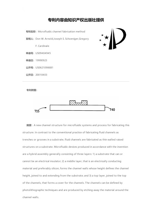
专利名称:Microfluidic channel fabrication method发明人:Don W. Arnold,Joseph S. Schoeniger,GregoryF. Cardinale申请号:US09404945申请日:19990923公开号:US06210986B1公开日:20010403专利内容由知识产权出版社提供专利附图:摘要:A new channel structure for microfluidic systems and process for fabricating this structure. In contrast to the conventional practice of fabricating fluid channels as trenches or grooves in a substrate, fluid channels are fabricated as thin walled raised structures on a substrate. Microfluidic devices produced in accordance with the invention are a hybrid assembly generally consisting of three layers: 1) a substrate that can or cannot be an electrical insulator; 2) a middle layer, that is an electrically conductingmaterial and preferably silicon, forms the channel walls whose height defines the channel height, joined to and extending from the substrate; and 3) a top layer, joined to the top of the channels, that forms a cover for the channels. The channels can be defined byphotolithographic techniques and are produced by etching away the material around the channel walls.申请人:SANDIA CORPORATION 代理人:D. A. Nissen更多信息请下载全文后查看。
聚酰亚胺基底上双光子直写负性光刻胶
第42卷第4期2021年4月激光杂志LASER JOURNALVol.42,No.4April,2021聚酰亚胺基底上双光子直写负性光刻胶杨公瑾,毛彦超,吴亚南,张宝森,刘建,毛淼,陈述郑州大学物理学院,郑卅450001摘要:近年来,聚酰亚胺薄膜因其良好的柔韧性、透明度、耐辐射等优点,逐渐成为制备柔性电子器件的重要材料。
利用飞秒激光双光子直写技术,以聚酰亚胺薄膜为基底,对负性光刻胶进行加工。
研究发现线条分辨率随着激光功率的降低和扫描速度的增加而提高,并获得了115nm最小线宽。
柔韧性测试实验表明,在聚酰亚胺薄膜上制备的亚波长线条具有很好的柔韧性。
这项工作证明了在聚酰亚胺薄膜上进行飞秒激光双光子直写的可行性,为进一步制造柔性电子器件提供了实验基础。
关键词:激光光学;飞秒激光;聚酰亚胺;双光子;光刻胶中图分类号:TN249文献标识码:A doi:10.14016/ki.jgzz.2021.04.021Two-photon direct writing of negative photoresist on a polyimide substrateYANG Gongjin,MAO Yanchao,WU Yanan,ZHANG Baosen,LIU Jian,MAO Miao,CHEN ShuSchool of Physics,Zhengzhou University,Zhengzhou450001,ChinaAbstract:In recent years,polyimide(PI)film has become an essential material for flexible electronic devices due to its advantages such as good flexibility,transparency,and radiation resistance.In this paper,femtosecond laser two-photon direct writing technology was employed for damaging photoresist fabrication on the PI substrate.The line resolution increases with decreasing laser power and increasing scanning speed,and a115nm lateral resolution was obtained.The flexibility test shows the excellent flexibility of the sub-wavelength lines fabricated on PI film.This work proves two-photon direct writing feasibility on PI film and provides fundamental experiments for further flexible electronic devices manufacture.Key words:laser optics;femtosecond laser;polyimide;two-photon;photoresist1引言近年来,柔性电子技术以其独特的柔性、延展性、高效性、低成本等特点,受到了人们的广泛关注。
石墨烯英文版
术语石墨烯首次出现在1987年,描述单石墨作为石墨层间化合物(GIC)的成分之一。 更大的石墨烯 分子或片(使得它们可以被认为是真正隔离的2D晶体)甚至在原理上也不能生长。 在20世纪30年代, Landau和Peierls(和Mermin,后来)显示热力学阻止2-d晶体在自由状态,物理今天的一篇文章
Introduction
Properties of graphene
Mechanical properties
- High Young’s modulus (~1,100 Gpa)高杨氏模量 High fracture strength (125 Gpa)高断裂强度 - Graphene is as the strongest material ever measured, some 200 times stronger than structural steel
• In 2004: Andre Geim and Kostya Novoselov at Manchester University managed to extract single-atom-thick crystallites (graphene) from bulk graphite: Pulled out graphene layers from graphite and transferred them onto thin silicon dioxide on a silicon wafer in a process sometimes called micromechanical cleavage or, simply, the Scotch tape technique. Since 2004, an explosion in the investigation of graphene in term of synthesis, characterization, properties as well as specifical potential application were reported. • 在2004年:曼彻斯特大学的Andre Geim和Kostya Novoselov设法从 块状石墨中提取单原子厚的微晶(石墨烯):从石墨中拉出石墨烯层 ,并将其转移到硅晶片上的薄二氧化硅上,有时称为微机械 切割, 或简单地,苏格兰带技术。 自2004年以来,报告了石墨烯在合成, 表征,性质以及特异性潜在应用方面的研究中的爆炸。
高分子专业英语课文翻译

A 高分子化学和高分子物理UNIT 1 What are Polymer?第一单元什么是高聚物?What are polymers? For one thing, they are complex and giant molecules and are different from low molecular weight compounds like, say, common salt. To contrast the difference, the molecular weight of common salt is only 58.5, while that of a polymer can be as high as several hundred thousand, even more than thousand thousands. These big molecules or ‘macro-molecules’ are made up of much smaller molecules, can be of one or more chemical compounds. To illustrate, imagine that a set of rings has the same size and is made of the same material. When these things are interlinked, the chain formed can be considered as representing a polymer from molecules of the same compound. Alternatively, individual rings could be of different sizes and materials, and interlinked to represent a polymer from molecules of different compounds.什么是高聚物?首先,他们是合成物和大分子,而且不同于低分子化合物,譬如说普通的盐。
- 1、下载文档前请自行甄别文档内容的完整性,平台不提供额外的编辑、内容补充、找答案等附加服务。
- 2、"仅部分预览"的文档,不可在线预览部分如存在完整性等问题,可反馈申请退款(可完整预览的文档不适用该条件!)。
- 3、如文档侵犯您的权益,请联系客服反馈,我们会尽快为您处理(人工客服工作时间:9:00-18:30)。
Fabrication of a hybrid graphene/layered double hydroxide materialHongjuan Li,Gang Zhu,Zong-Huai Liu *,Zupei Yang,Zenglin WangKey Laboratory of Applied Surface and Colloid Chemistry (Shaanxi Normal University),Ministry of Education,Xi’an 710062,PR China School of Chemistry and Materials Science,Shaanxi Normal University,Xi’an 710062,PR ChinaA R T I C L E I N F O Article history:Received 7May 2010Accepted 29July 2010Available online 5August 2010A B S T R A C TA hybrid graphene/Ni 2+–Fe 3+layered double hydroxide material has been fabricated by the hydrothermal treatment of a mixed suspension of the exfoliated graphite oxide,Ni(NO 3)26H 2O,Fe(NO 3)3Æ9H 2O,urea and trisodium citrate.The Ni 2+–Fe 3+layered double hydroxide platelets are first homogeneously grown on the surface of GO nanosheets which are then reduced to graphene under a mild hydrothermal treatment.In the hybrid graphene/Ni 2+–Fe 3+layered double hydroxide material,the restacking of graphene nanosheets is effec-tively prevented by the formation of Ni 2+–Fe 3+layered double hydroxide platelets,and the graphene nanosheets exist in a complete exfoliation state.Ó2010Elsevier Ltd.All rights reserved.1.IntroductionSince the isolation of single-layer graphene in 2004,the prep-aration,structure and application of graphene have been widely researched because of its good electrical and thermal conductivity [1–3].In company with the recent achievement of large-area,free-standing graphenes,graphenes show pro-spective application in many fields,particularly in electronic and optoelectronic systems [4,5].However,some disadvan-tages are also found in the intrinsic property of graphene [6],which limit its applicability.Graphene-based hybrid mate-rials are quite intriguing from the perspectives of both funda-mental science and technology because the hybrid can enable versatile and tailor-made properties with performances far beyond those of the individual materials.Up to now,many graphene-based hybrid materials from graphene and certain functional particles such as polymers,metal oxides,metal particles,and organic molecules have been prepared.They present unique features and can be used in potential elec-trode materials,catalysts,biosensors,and methanol fuel cells,and so on [7–13].Ni and Fe are important transition metals due to their no-vel electronic,magnetic and optical properties.The compounds that they consist of such as layered double hydroxide (LDH)show a wide application in electro-and photoactive materi-als,catalysts,flame retardants,acid absorbents,anion exchangers,and so forth [14–16].Research results show that the composition and degree of crystallinity,the crystallite size and the size distribution affect the potential applications of LDH materials [17,18].Thus the synthesis of the transition metal layered composites such as Ni 2+–Fe 3+(or Ni 2+–Co 2+–Fe 3+)LDH with high crystallinity and well-defined hexagonal shape is of interest to probe LDH materials with novel elec-tronic,magnetic and optical properties.We have prepared Ni 2+–Fe 3+LDH material with high crystallinity and well-de-fined hexagonal shape by using urea as hydrolysis agent and trisodium citrate as complexing agent [19].In this work,we reported a simple synthesis of a hybrid graphene/Ni 2+–Fe 3+LDH material under mild hydrothermal condition.In the synthesis procedure,the exfoliated graphite oxide (GO)is simultaneously reduced to graphene in company with the homogeneous precipitation of Ni 2+–Fe 3+LDH.0008-6223/$-see front matter Ó2010Elsevier Ltd.All rights reserved.doi:10.1016/j.carbon.2010.07.053*Corresponding author at:Key Laboratory of Applied Surface and Colloid Chemistry (Shaanxi Normal University),Ministry of Education,Xi’an 710062,PR China.Tel.:+862985308442;fax:+862985307774.E-mail address:zhliu@ (Z.-H.Liu).2.Experimental2.1.MaterialsCrudeflake graphite(carbon content:99.9%)was purchased from Qingdao Aoke Co.,China.Tetramethylammonium hydroxide(TMAOH)(25wt.%)was purchased from Alfa Aesar Co.,H2O2(30%),H2SO4(98%),KMnO4,NaNO3,Ni(NO3)2Æ6H2O, Fe(NO3)3Æ9H2O,urea and trisodium citrate(TSC)were analyti-cal grade and used without further purification.Deionized water was used throughout the experiments.2.2.Synthesis and delamination of graphite oxideThe starting material,GO,was prepared from natural graphite by the Hummers method[20].GO sample(0.5g)was soaked in an aqueous solution of TMAOH(100mL,0.22mol LÀ1)for 7days at room temperature.After soaking,the colloidal sus-pension was separated by centrifugation and washing with deionized water several times until the pH was7,and the del-aminated GO slurry was obtained.2.3.Synthesis of the hybrid graphene/Ni2+–Fe3+LDH materialT ypically,Ni(NO3)2Æ6H2O,Fe(NO3)3Æ9H2O,urea and TSC were mixed together and dissolved in80mL of deionized water to give thefinal concentrations of16,respectively.The mixture wasminated GO slurry with vigorousinto Teflon-lined stainless steelmally treated at150°C for2days.Thewas centrifuged and washed within air,which was abbreviated asTo compare with the aboveexfoliated GO suspension was150°C for2days at the sameresulting product wasfiltered,washedand dried in air,which was2.4.CharacterizationX-ray diffraction(XRD)analysis was3c X-ray diffractometer with Cu K a(operation voltage and current of40tively.Transmission electroncollected using a JEOL-JEM-3010120kV.Specimens for observationing the samples into alcohol bydropped on carbon–copper grids.Theken at room temperature in theusing an ALMEGA–TM Ramanspectra were recorded using a532nmmogravimetry(TG)and differential(DSC)measurements were obtained(Q1000DSC+LNCS+FACS Q600SDT)10°C min–1.Ni and Fe contents weretively coupled plasma(ICP)atomic(IRIS Advantage)after dissolving awith an aqueous HCl solution.XPS formed with an Axis Ultra,kratos(UK)spectrometer using Al K a radiation(1486eV)at a power of150W(accelerating voltage15kV)in a vacuum of10À9Tom.The pH titration mea-surements were performed with an Orion960automatic titra-tor,and volumetric standard NaOH(0.01mol LÀ1)was used as the titrant.Before the titration experiment,GO sample(about 20mg)was dispersed in0.1mol LÀ1aqueous solution of NaCl (50mL)and then stirred for3h.3.Results and discussionThe XRD patterns of the precursor GO,the delaminated GO slurry,and the hybrid RGO–Ni–Fe LDH material are shown in Fig.1.The precursor,GO,has a layered structure with a basal spacing of0.82nm,showing the complete oxidation of graph-ite into the graphite oxide[21].After GO is treated with TMAOH solution at a molar ratio of the TMA l/GO s=5(added TMA+ion amount in the solution to the ion exchange capacity of GO)for7days,the obtained suspensions are centrifuged, and the colloidal sediments are subjected to XRD measure-ment in the wet state.The XRD pattern of the sediments ob-tained gives no clear peaks but only abroad diffraction halo in a2h range of20°–40°,in striking contrast to that of starting GO.The broad halo is most likely related to scattering from dispersed single sheets of GO and water as a solvent,which is similar to the case of layered titanic acid and manganese oxide[22,23].The broad halo indicates that the stacked sheetsFig.1–XRD patterns of the precursor GO,the delaminated GO slurry,and the hybrid RGO–Ni–Fe LDH material, respectively.4392C A R B O N48(2010)4391–4396GO is mainly reduced to graphene in the hybrid RGO–Ni–Fe LDH material.The result is also supported by the C1s XPSspectra of GO and the hybrid RGO–Ni–Fe LDH material (Fig.2).The C1s XPS spectrum of GO clearly indicates a con-siderable degree of oxidation,with three different compo-nents corresponding to carbon atoms in different functional groups:the non-oxygenated ring C(C–C),the C in C–O bonds (C–O),and the carboxylate carbon(O–C@O)[30,31].The areas of the three C1s components of graphite oxide show that the non-oxygenated ring C is about41%(284.5eV),while that of ponent is dissolved and the residual sediment is used to investigate the reduction behavior of GO to graphene.The residual sediment is washed with distilled water and dried for1day at room temperature.The XRD pattern of the ob-tained sample is shown in Fig.3.A broad peak with a basal spacing of0.36nm at2h=24.8°is observed,and it can be as-cribed to the characteristic peak of graphene[32].This result suggests that GO nanosheets are completely reduced into graphene in the hybrid RGO–Ni–Fe LDH material.In contrast, only the colloidal dispersion of GO is hydrothermally treated at150°C for2days,and the XRD pattern of the obtained sam-ple is shown in Fig.3.A clear change of the XRD patterns can be observed,and the basal spacing is reduced from0.82nm of the pristine GO to0.34nm.Meanwhile,the broad peak is very similar to that of the obtained sample after the hybrid RGO–Ni–Fe LDH material is treated with HCl solution.This result also directly proves the reduction of the GO to graphene and the formation of the RGO–Ni–Fe LDH hybrid material.The Raman spectra of the pristine GO,RGO,and the hybrid RGO–Ni–Fe LDH material in the range from400to3000cm–1 are shown in Fig.4.The G line around1597cm–1and the D line around1344cm–1are observed in the Raman spectrum of the pristine GO.In general,the G line is assigned to the E2g phonon of C sp2atoms,while the D line is a breathing mode of r-point phonons of A1g symmetry[33,34].Meanwhile, the second-order band(2D band)around2895cm–1is also ob-served,which results from a double-resonance process and links the phonon wave vectors to the electronic band struc-ture[35].On the other hand,two obvious change of Raman spectrum are found for the samples of RGO and the hybrid RGO–Ni–Fe LDH material.The second-order band around 2895cm–1disappears and the relative peak intensity of the D line to G line(I D/I G intensity)changes.In general,the I D/I G intensity ratio is a measure of disorder degree and average size of the sp2domains in graphite materials[36].The exper-imental results show that the I D/I G intensity ratio is higher than that of the pristine GO for the samples of RGO and the hybrid RGO–Ni–Fe LDH material.We think that two reasons cause the changes.One is the significant decrease of the sizeFig.2–The C1s XPS spectra of GO and the hybrid RGO–Ni–Fe LDH material.Fig.3–XRD patterns of the residual sediment obtained from the HCl leaching of the hybrid RGO–Ni–Fe LDH material and RGO.the in-plane sp 2domains due to the reduction of the exfo-liated GO [37],and the other is the remove of the oxygen func-tional groups in graphite oxide sheets and the restablishment the conjugated graphene network (sp 2carbon)[32].In addi-tion,the weak band around 563cm –1for the lattice vibration the hydroxyl layers is observed in the hybrid RGO–Ni–Fe LDH material.TEM image of the hybrid RGO–Ni–Fe LDH material shows that both irregular and thin hexagonal platelets with a mean lateral size of 350nm of Ni 2+–Fe 3+LDH nanosheets and the corrugation and scrolling image of graphene nanosheets can be observed (Fig.5).The result indicates that the platelets of Ni 2+–Fe 3+LDH are decorated in the graphene nanosheets to form the hybrid RGO–Ni–Fe LDH material.Since Ni 2+–Fe 3+LDH nanosheets are distributed on the surfaces of graphene nanosheets,the restacking of graphene nanosheets will be effectively prevented and the XRD pattern characteristic peak of graphene is not observed.For the reduced graphene,the similar crumpled silk-like image of graphene nanosheets is also observed in sample RGO in the control experiment.The result also supports the conclusion that the GO nanosheets in hybrid RGO–Ni–Fe LDH material are reduced to graphene.From the HRTEM image of the hybrid RGO–Ni–Fe LDH mate-rial,two kinds of contrast fringes can be observed.The lattice fringe with an interplanar distance of 0.23nm is ascribed to the (015)plane of the hexagonal Ni 2+–Fe 3+LDH,while the lat-tice fringe with a relative wide d -spacing of 0.52nm is caused by the ordered graphite lattices embed in the Ni 2+–Fe 3+LDH lattice fringes.The relative wide d-spacing between graphene nanosheets (0.52nm)is larger than that of graphite (0.34nm),indicating an interlayer distance increase of graphene nano-sheets after the reassembling reaction.The thermal behaviors of the pristine GO,RGO,and the hy-brid RGO–Ni–Fe LDH material are investigated by thermograv-metric analysis (TGA)in dry air.The pristine GO exhibits two steps of significant drops in mass at 229and 637°C (Fig.6),which are attributed to the removal of oxygen–functional groups and the combustion of the carbon skeleton of GO,respectively [6,24].As shown in Fig.6,RGO prepared in theFig.4–The Raman spectra of the hybrid RGO–Ni–Fe LDH material,RGO and GO.Fig.5–TEM images of the hybrid RGO–Ni–Fe LDH material,RGO and HRTEM image of the hybrid RGO–Ni–Fe LDH material,respectively.6–TGA curves of the precursor GO,RGO and the hybrid RGO–Ni–Fe LDH material,respectively.control experiment exhibits only one step of mass loss at 558°C,which corresponds to the combustion of the carbon skeleton[25].The result suggests that most of the oxygen-containing groups of the pristine GO have been removed dur-ing the hydrothermal reduction process,and it is probably an-other prove of the reduction of the pristine GO to graphene. On the other hand,some obvious changes can be observed in the DSC curve of the hybrid RGO–Ni–Fe LDH material. The two new endothermic peaks at around167and304°C are ascribed to the release of the interlayer water and the dehydroxylation of Ni2+–Fe3+LDH nanolayers in the hybrid RGO–Ni–Fe LDH material,respectively[38].Meanwhile,the exothermic peak at about398°C is attributed to the combus-tion of the carbon skeleton,which shifts to a relative lower temperature in compare with that of the pristine GO.The re-sult suggests that both the oxygenated functional groups and the thermal stability are decreased in compare with the bulk graphite powder.Similar results are observed in the litera-tures[25,39],and the reason may be attributed to the interac-tion between graphene nanosheets and Ni2+–Fe3+LDH nanosheets.The weight loss between270and520°C is about 25.3%,which corresponds to the combustion of the reduced graphene.The value is similar to the experiment one(about 26.6%)from the residual sediment obtained after the acid treatment of the hybrid RGO–Ni–Fe LDH material.According to the above results,a schematic representation of the formation process of the hybrid RGO–Ni–Fe LDH mate-rial is given in Fig.7.The pristine,GO,has a layered structure with a basal spacing of0.82nm,containing one molecular layer of water between the graphite oxide sheets.The TMA+ ions are intercalated into the interlayers of GO and followed by water washing,which results in an exfoliation of GO nano-sheets.When the slurry of exfoliated GO is soaked in a mixed solution of Ni(NO3)2Æ6H2O,Fe(NO3)3Æ9H2O,urea and TSC,metal salts can be adsorbed on the surface of GO nanosheets,and Ni2+–Fe3+LDH platelets are grown on the surface of graphene nanosheets in company with a reduction process of the pris-tine GO to graphene under a hydrothermal treatment.The Ni2+–Fe3+LDH platelets are intercalated into the nanosheets of graphene,which effectively prevents the restacking of the as-reduced graphene nanosheets[25]and the hybrid RGO–Ni–Fe LDH material isfinally obtained.4.ConclusionsA hybrid graphene/Ni2+–Fe3+LDH material has been fabri-cated by the hydrothermal treatment of a mixed suspension of the exfoliated GO,Ni(NO3)2Æ6H2O,Fe(NO3)3Æ9H2O,urea and trisodium citrate.In company with the homogeneously pre-cipitation of Ni2+–Fe3+LDH platelets on the surface of GO nanosheets,GO nanosheets are simultaneously reduced into graphene.The as-reduced graphene nanosheets exist in a complete exfoliation state in the hybrid RGO–Ni–Fe LDH material due to the formation of Ni2+–Fe3+LDH platelets, which are deposited randomly on the graphene nanosheets and prevent the restacking of the as-reduced graphene nanosheets.AcknowledgmentsWe thank National High Technology Research and Develop-ment Program of China(2007AA03Z248)and National Natural Science Foundation of China(20971082)forfinancial support this research.R E F E R E N C E S[1]Rao CNR,Biswas K,Subrahmanyama KS,Govindaraj A.Graphene,the new nanocarbon.J Mater Chem2009;19(17):2457–69.[2]Geim AK.Graphene:status and prospects.Science2009;324(5934):1530–4.[3]Rao CNR,Sood AK,Subrahmanyam KS,Govindaraj A.Graphene:the new two-dimensional nanomaterial.Angew Chem Int Ed2009;48(42):7752–78.[4]Mattevi C,Eda G,Agnoli S,Miller S,Mkhoyan KA,Celik O,et al.Evolution of electrical,chemical,and structuralproperties of transparent and conducting chemically derived graphene thinfilms.Adv Funct Mater2009;19(16):2577–83. [5]Novoselov KS,Geim AK,Morozov SV,Jiang D,Katsnelson MI,Grigorieva IV,et al.T wo-dimensional gas of massless dirac fermions in graphene.Nature2005;438(7065):197–200.[6]Meyer JC,Geim AK,Katsnelson MI,Novoselov KS,Booth TJ,Roth S.The structure of suspended graphene sheets.Nature 2007;446(7131):60–3.[7]Kong BS,Geng JX,Jung yer-by-layer assembly ofgraphene and gold nanoparticles by vacuumfiltration and spontaneous reduction of gold ions.Chem Commun2009;16:2174–6.[8]Muszynski R,Seger B,Kamat PV.Decorating graphene sheetswith gold nanoparticles.J Phys Chem C2008;112(14):5263–6.[9]Williams G,Seger B,Kamat PV.TiO2–graphenenanocomposites.UV-assisted photocatalytic reduction ofgraphene oxide.ACS Nano2008;2(7):1487–91.[10]Lu J,Do I,Drzal LT,Worden RM,Lee I.Nanometal-decoratedexfoliated graphite nanoplatelet based glucose biosensorsFig.7–A schematic representation of the formation process of the hybrid RGO–Ni–Fe LDH material.with high sensitivity and fast response.ACS Nano2008;2(9):1825–32.[11]Xu C,Wang X,Zhu JW,Yang XJ,Lu LD.Deposition of Co3O4nanoparticles onto exfoliated graphite oxide sheets.J Mater Chem2008;18(46):5625–9.[12]Wang DW,Li F,Zhao JP,Ren WC,Chen ZG,Tan J,et al.Fabrication of graphene/polyaniline composite paper viain situ anodic electropolymerization for high-performance flexible electrode.ACS Nano2009;3(7):1745–52.[13]Si Y,Samulski ET.Exfoliated graphene separated by platinumnanoparticles.Chem Mater2008;20(21):6792–6.[14]Li F,Liu JJ,Evans DG,Duan X.Stoichiometric synthesis ofpure MFe2O4(M@Mg,Co,and Ni)spinel ferrites from tailored layered double hydroxide(hydrotalcite-like)precursors.Chem Mater2004;16(8):1597–602.[15]Kumbhar PS,Sanchez-Valente J,Millet JMM,Figueras F.Mg–Fehydrotalcite as a catalyst for the reduction of aromatic nitro compounds with hydrazine hydrate.J Catal2000;191(2):467–73.[16]Xiang X,Hima HI,Wang H,Li F.Facile synthesis and catalyticproperties of nickel-based mixed-metal oxides withmesopore networks from a novel hybrid compositeprecursor.Chem Mater2008;20(3):1173–82.[17]Liu ZP,Ma RZ,Ebina Y,Iyi N,Takada K,Sasaki T.Generalsynthesis and delamination of highly crystalline transition-metal-bearing layered double ngmuir2007;23(2):861–7.[18]Iyi N,Fujii K,Okamoto K,Sasaki T.Factors influencing thehydration of layered double hydroxides(LDHs)and theappearance of an intermediate second staging phase.Appl Clay Sci2007;35(3–4):218–27.[19]Han YF,Liu ZH,Yang ZP,Wang ZL,Tang XH,Wang T,et al.Preparation of Ni2+ÀFe3+layered double hydroxide material with high crystallinity and well-defined hexagonal shapes.Chem Mater2008;20(2):360–3.[20]Hummers WS,Offeman RE.Preparation of graphitic oxide.JAm Chem Soc1958;80(6):1339.[21]Liu ZH,Wang ZM,Yang XJ,Ooi K.Intercalation of organicammonium ions into layered graphite ngmuir2002;18(12):4926–32.[22]Liu ZH,Ooi K,Kanoh H,Tang W,Tomida T.Swelling anddelamination behaviors of birnessite-type manganese oxide by intercalation of tetraalkylammonium ngmuir2000;16(9):4154–64.[23]Sasaki T,Watanabe M.Osmotic swelling to exfoliation.Exceptionally high degrees of hydration of a layered titanate.J Am Chem Soc1998;120(19):4682–9.[24]Matsuo Y,Tahara K,Sugie Y.Structure and thermalproperties of poly(ethylene oxide)-intercalated graphiteoxide.Carbon1997;35(1):113–20.[25]Xu C,Wang X,Zhu JW.Graphene-metal particlenanocomposites.J Phys Chem C2008;112(50):19841–5. [26]Cai DY,Song M.Preparation of fully exfoliated graphite oxidenanoplatelets in organic solvents.J Mater Chem2007;17(35):3678–80.[27]Nethravathi C,Nisha T,Ravishankar N,Shivakumara C,Rajamathi M.Graphene-nanocrystalline metal sulphidecomposites produced by a one-pot reaction starting fromgraphite oxide.Carbon2009;47(8):2054–9.[28]Lambert TN,Chavez CA,Hernandez–Sanchez B,Lu P,Bell NS,Ambrosini A,et al.Sonochemical one-pot synthesis ofcarbon nanotube-supported rhodium nanoparticles forroom-temperature hydrogenation of arenes.J Phys Chem C 2009;113(40):19812–23.[29]Xu C,Wu XD,Zhu JW,Wang X.Synthesis of amphiphilicgraphite oxide.Carbon2008;46(2):386–9.[30]Briggs D,Beamson G.High resolution XPS of organicpolymers:the Scienta ESCA300database.New York:JohnWiley and Sons;1992.[31]Waltman RJ,Pacansky J,Bates Jr CW.X-ray photoelectronspectroscopic studies on organic photoconductors:evaluation of atomic charges on chlorodiane blue andp-(diethylamino)benzaldehyde diphenylhydrazone.ChemMater1993;5(12):1799–804.[32]Wang GX,Yang J,Park JS,Gou XL,Wang B,Liu H,et al.Facilesynthesis and characterization of graphene nanosheets.J Phys Chem C2008;112(22):8192–5.[33]T uinstra F,Koenig JL.Raman spectrum of graphite.J ChemPhys1970;53(3):1126–30.[34]Ferrari AC,Robertson J.Interpretation of Raman spectra ofdisordered and amorphous carbon.Phys Rev B2000;61(20):14095–107.[35]Reina A,Jia XT,Ho J,Nezich D,Son H,Bulovic V,et rgearea,few-layer graphenefilms on arbitrary substrates bychemical vapor deposition.Nano Lett2009;9(1):30–5.[36]Navarro C,Weitz RT,Bittner AM,Scolari M,Mews A,BurghardM,et al.Electronic transport properties of individualchemically reduced graphene oxide sheets.Nano Lett2007;7(11):3499–503.[37]Stankovich S,Dikin AA,Piner RD,Kohlhass KA,Kleinhammes A,Jia YY,et al.Synthesis of graphene-based nanosheets via chemical reduction of exfoliated graphiteoxide.Carbon2007;45(7):1558–65.[38]Kovanda F,Grygar T,Dornicˇca´k V.Thermal behaviour ofNi–Mn layered double hydroxide and characterization offormed oxides.Solid State Sci2003;5(7):1019–26.[39]Wu JL,Shen XP,Jiang L,Wang K,Chen KM.Solvothermalsynthesis and characterization of sandwich-like graphene/ ZnO nanocomposites.Appl Surf Sci2010;256(9):2826–30.4396C A R B O N48(2010)4391–4396。
