WP4060VH2YD;中文规格书,Datasheet资料
B0540WS-7;中文规格书,Datasheet资料
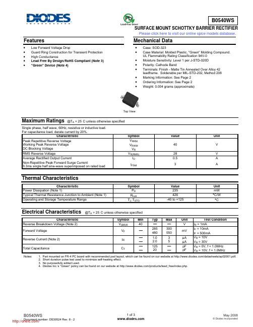
SURFACE MOUNT SCHOTTKY BARRIER RECTIFIERFeatures• Low Forward Voltage Drop• Guard Ring Construction for Transient Protection • High Conductance• Lead Free By Design/RoHS Compliant (Note 3) • "Green" Device (Note 4)Mechanical Data• Case: SOD-323• Case Material: Molded Plastic, "Green" Molding Compound.UL Flammability Rating Classification 94V-0• Moisture Sensitivity: Level 1 per J-STD-020D• Polarity: Cathode Band• Terminals: Finish - Matte Tin Annealed Over Alloy 42leadframe. Solderable per MIL-STD-202, Method 208 • Marking Information: See Page 2• Ordering Information: See Page 2• Weight: 0.004 grams (approximate)Top ViewMaximum Ratings@T A = 25°C unless otherwise specifiedSingle phase, half wave, 60Hz, resistive or inductive load.For capacitance load, derate current by 20%.Characteristic Symbol Value UnitPeak Repetitive Reverse Voltage Working Peak Reverse Voltage DC Blocking Voltage V RRMV RWMV R40 VRMS Reverse Voltage V R(RMS)28 V Average Rectified Output Current I O0.5 ANon-Repetitive Peak Forward Surge Current8.3ms single half sine-wave superimposed on rated load I FSM3 A Thermal CharacteristicsCharacteristic Symbol Value Unit Power Dissipation (Note 1) P D235 mW Typical Thermal Resistance Junction to Ambient (Note 1) RθJA426 °C/W Operating and Storage Temperature Range T J, T STG-40 to +125 °CElectrical Characteristics@T A = 25°C unless otherwise specifiedCharacteristic Symbol Min Typ Max Unit Test Condition Reverse Breakdown Voltage (Note 2) V(BR)R40 ⎯⎯V I R = 1mAForward Voltage V F⎯285480300550mVI F = 10mAI F = 500mAReverse Current (Note 2) I R ⎯⎯1.02.035μAμAV R = 10VV R = 30VTotal Capacitance C T ⎯⎯12520⎯⎯pFpFV R = 0V, f = 1.0MHzV R = 10V, f = 1.0MHzNotes: 1. Part mounted on FR-4 PC board with recommended pad layout, which can be found on our website at /datasheets/ap02001.pdf.2. Short duration pulse test used to minimize self-heating effect.3. No purposefully added Lead.4. Diodes Inc.'s "Green" policy can be found on our website at /products/lead_free/index.php.Please click here to visit our online spice models database.10100V, INSTANTANEOUS REVERSE VOLTAGE (V)Fig. 2 Typical Reverse CharacteristicsRI,INSTANTANEOUSFORWARDCURRENT(mA)FV, INSTANTANEOUS FORWARD VOLTAGE (V)Fig. 1 Typical Forward CharacteristicsF100C,TOTALCAPACITANCE(pF)TV, DC REVERSE VOLTAGE (V)Fig. 3 Total Capacitance vs. Reverse VoltageR0.250.50050100I,AVE150RAGEFORWARDCURRENT(A)F(AV)T, TERMINAL TEMPERATURE (C)Fig. 4 Forward Current Derating CurveT°0.751.02575125Ordering Information(Note 5)Part Number Case PackagingB0540WS-7 SOD-323 3000/Tape & ReelNotes: 5. For packaging details, go to our website at /datasheets/ap02007.pdf.Marking InformationSF SF = Product Type Marking CodePackage Outline DimensionsSuggested Pad LayoutIMPORTANT NOTICEDiodes Incorporated and its subsidiaries reserve the right to make modifications, enhancements, improvements, corrections or other changes without further notice to any product herein. Diodes Incorporated does not assume any liability arising out of the application or use of any product described herein; neither does it convey any license under its patent rights, nor the rights of others. The user of products in such applications shall assume all risks of such use and will agree to hold Diodes Incorporated and all the companies whose products are represented on our website, harmless against all damages.LIFE SUPPORTDiodes Incorporated products are not authorized for use as critical components in life support devices or systems without the expressed written approval of the President of Diodes Incorporated.SOD-323 Dim Min Max A 0.25 0.35 B 1.20 1.40 C 2.30 2.70 H 1.60 1.80 J 0.00 0.10 K 1.0 1.1 L0.20 0.40 M 0.10 0.15α0° 8°All Dimensions in mmDimensions Value (in mm)Z 3.75 G 1.05 X 0.65 Y 1.35 C 2.40分销商库存信息: DIODESB0540WS-7。
FGH40N60SMD;中文规格书,Datasheet资料

Typ.
-
Max.
0.43 1.5 40
Package Marking and Ordering Information
Device Marking
Device
FGH40N60SMD
FGH40N60SMD
Package
TO-247
Reel Size
-
Tape Width
-
Units
oC/W oC/W oC/W
IF = 20A
TC = 25oC TC = 175oC
Erec
Reverse Recovery Energy
TC = 175oC
trr
Diode Reverse Recovery Time IF =20A, dIF/dt = 200A/ms
TC = 25oC TC = 175oC
Qrr
Diode Reverse Recovery Charge
TC = 25oC TC = 175oC
Min.
-
Typ.
2.3 1.67 48.9 36 110 46.8 445
Max
2.8 -
Unit s
V uJ ns
nC
FGH40N60SMD Rev. A
3
/
FGH40N60SMD 600V, 40A Field Stop IGBT
100
20V
12V
15V
10V
Collector Current, IC [A]
Collector Current, IC [A]
80
80
60
60
VGE = 8V
VGE = 8V
40
WP4060VH2GD;中文规格书,Datasheet资料
PACKING & LABEL SPECIFICATIONS
ቤተ መጻሕፍቲ ባይዱ
WP4060VH/2GD
SPEC NO: DSAE9382 APPROVED: WYNEC
REV NO: V.11 CHECKED: Allen Liu
DATE: APR/07/2011 DRAWN: J.Yu
PAGE: 4 OF 5 ERP: 1102013558
SPEC NO: DSAE9382 APPROVED: WYNEC
REV NO: V.11 CHECKED: Allen Liu
DATE: APR/07/2011 DRAWN: J.Yu
PAGE: 1 OF 5 ERP: 1102013558
/
Selection Guide
Notes: 1.Wavelength: +/-1nm. 2. Forward Voltage: +/-0.1V.
Absolute Maximum Ratings at TA=25°C
Parameter Power dissipation DC Forward Current Peak Forward Current [1] Reverse Voltage Operating/Storage Temperature Lead Solder Temperature [2] Lead Solder Temperature [3]
/
SPEC NO: DSAE9382 APPROVED: WYNEC
REV NO: V.11 CHECKED: Allen Liu
DATE: APR/07/2011 DRAWN: J.Yu
PAGE: 5 OF 5 ERP: 1102013558
WSL40261L000FEB;WSL40262L000FEB;WSL4026L5000FEB;WSL4026L3000FEB;中文规格书,Datasheet资料
GLOBAL PART NUMBER INFORMATION
Global Part Numbering example: WSL4026L5000FEA (WSL4026, 0.0005 , ± 1 %)
W
S
L
4
0
2
6
L
5
0
0
0
F
E
A
SPECIAL (Dash number) (Up to 2 digits) From 1 to 99 as applicable
TECHNICAL SPECIFICATIONS
PARAMETER Temperature coefficient Operating temperature range Maximum working voltage UNIT ppm/°C °C V RESISTOR CHARACTERISTICS ± 75 over temperature of + 20 °C to + 60 °C - 65 to + 170 (P x R)1/2
Legal Disclaimer Notice
Vishay
Disclaimer
ALL PRODUCT, PRODUCT SPECIFICATIONS AND DATA ARE SUBJECT TO CHANGE WITHOUT NOTICE TO IMPROVE RELIABILITY, FUNCTION OR DESIGN OR OTHERWISE. Vishay Intertechnology, Inc., its affiliates, agents, and employees, and all persons acting on its or their behalf (collectively, “Vishay”), disclaim any and all liability for any errors, inaccuracies or incompleteness contained in any datasheet or in any other disclosure relating to any product. Vishay makes no warranty, representation or guarantee regarding the suitability of the products for any particular purpose or the continuing production of any product. To the maximum extent permitted by applicable law, Vishay disclaims (i) any and all liability arising out of the application or use of any product, (ii) any and all liability, including without limitation special, consequential or incidental damages, and (iii) any and all implied warranties, including warranties of fitness for particular purpose, non-infringement and merchantability. Statements regarding the suitability of products for certain types of applications are based on Vishay’s knowledge of typical requirements that are often placed on Vishay products in generic applications. Such statements are not binding statements about the suitability of products for a particular application. It is the customer’s responsibility to validate that a particular product with the properties described in the product specification is suitable for use in a particular application. Parameters provided in datasheets and/or specifications may vary in different applications and performance may vary over time. All operating parameters, including typical parameters, must be validated for each customer application by the customer’s technical experts. Product specifications do not expand or otherwise modify Vishay’s terms and conditions of purchase, including but not limited to the warranty expressed therein. Except as expressly indicated in writing, Vishay products are not designed for use in medical, life-saving, or life-sustaining applications or for any other application in which the failure of the Vishay product could result in personal injury or death. Customers using or selling Vishay products not expressly indicated for use in such applications do so at their own risk and agree to fully indemnify and hold Vishay and its distributors harmless from and against any and all claims, liabilities, expenses and damages arising or resulting in connection with such use or sale, including attorneys fees, even if such claim alleges that Vishay or its distributor was negligent regarding the design or manufacture of the part. Please contact authorized Vishay personnel to obtain written terms and conditions regarding products designed for such applications. No license, express or implied, by estoppel or otherwise, to any intellectual property rights is granted by this document or by any conduct of Vishay. Product names and markings noted herein may be trademarks of their respective owners.
slf系列贴片电感datasheet
特点 ●是最适用于电源系统的低直流电阻,大电流,节能型产品。 ●因采用磁力屏蔽结构,所以可实现高密度安装。 ●底面为平直的低背型 , 可稳定地安装在电路板上。 ●采用卷带仕样,支持自动插入机。 用途 手机,计算机,硬盘驱动器,其他各种电子设备 仕样
工作温度范围 保存温度范围 –20 to +85°C [包括自身温度上升] –40 to +85°C [产品单体]
电气特性
电感 (H) 4.7 6.8 10 15 22 33 47 68 100 150 220 电感容差 ±20% ±20% ±20% ±20% ±20% ±20% ±20% ±20% ±20% ±20% ±20% L 测定频率 (kHz) 100 100 100 100 100 100 100 100 100 100 100 直流电阻 ( )±20% 0.0284 0.0354 0.0532 0.0745 0.104 0.148 0.21 0.29 0.43 0.65 0.98 额定电流 (A) 基于电感 变化率时 1.6max. 1.5max. 1.3max. 1max. 0.77max. 0.69max. 0.59max. 0.5max. 0.42max. 0.34max. 0.26max. 基于温度 上升时 2.5typ. 2.2typ. 1.8typ. 1.4typ. 1.3typ. 1.1typ. 0.92typ. 0.78typ. 0.64typ. 0.5typ. 0.38typ. 品名 SLF6028T-4R7M1R6-PF SLF6028T-6R8M1R5-PF SLF6028T-100M1R3-PF SLF6028T-150M1R0-PF SLF6028T-220MR77-PF SLF6028T-330MR69-PF SLF6028T-470MR59-PF SLF6028T-680MR50-PF SLF6028T-101MR42-PF SLF6028T-151MR34-PF SLF6028T-221MR26-PF
SI2302-TP;中文规格书,Datasheet资料

Revision: A
/
3 of 5
2011/01/01
VGS, Gate to Source Voltage (V) ID, Drain Current (A)
VTH, Normalized Gate-Source Threshold Voltage
RDS(ON), Normalized RDS(ON), On-Resistance(Ohms)
IS, Source-drain current (A)
ID, Drain Current (A)
SI2302
10 25 C
Maximum Ratings @ 25OC Unless Otherwise Specified
Symbol VDS ID IDM VGS
PD R©JA
TJ
TSTG
Parameter Drain-source Voltage Drain Current-Continuous Drain Current-Pulsed a Gate-source Voltage
MCC
TM
Micro Commercial Components
5 VDS=10V ID=3.6A
4
3
2
1
0
0
2
4
6
Qg, Total Gate Charge (nC)
Figure 7. Gate Charge
VDD
RL VIN
D
VOUT
VGS
RGEN G
S
Figure 9. Switching Test Circuit
DMN4060SVT-7;中文规格书,Datasheet资料

2011 Y
Jan
Feb
1
2
2012 Z
Mar 3
2013 A
Apr
May
45Biblioteka 2014 BJun
Jul
6
7
2015 C
Aug
Sep
8
9
2016 D
Oct O
2017 E
Nov
Dec
N
D
DMN4060SVT
http://onDeocicum.ceonmt n/umber: DS35702 Rev. 2 - 2
Units
W
°C/W °C/W
W
°C/W °C/W °C/W
°C
P(PK), PEAK TRANSIENT POIWER (W)
100 80 60
Single Pulse RθJA = 72°C/W RθJA(t) = r(t) * RθJA TJ - TA = P * RθJA(t)
40
20
0 0.0001 0.001 0.01 0.1 1 10 100 1,000
Source
Equivalent Circuit
Ordering Information (Note 3)
Notes:
Part Number DMN4060SVT-7
Case TSOT26
Packaging 3,000/Tape & Reel
1. EU Directive 2002/95/EC (RoHS) & 2011/65/EU (RoHS 2) compliant. No purposely added lead. Halogen and Antimony free. 2. Diodes Inc.’s “Green” policy can be found on our website at . 3. For packaging details, go to our website at .
wp一40数显表说明书

wp一40数显表说明书WP-140 Digital Display Meter User ManualIntroduction:The WP-140 digital display meter is a versatile and reliable tool used in various industries for precise measurement and monitoring. This user manual aims to provide a comprehensive understanding of the functions and operations of the WP-140, empowering users to make the most of this advanced measurement instrument.1. Overview of the WP-140 Digital Display Meter:The WP-140 digital display meter features a high-resolution LCD screen with clear and easy-to-read numerical values. It supports multiple measurement parameters, including voltage, current, resistance, frequency, and temperature. The compact and lightweight design ensures portability while maintaining accuracy in measurements.2. Basic Operations:2.1 Power On/Off:To turn on the WP-140 meter, press and hold the power button for a few seconds until the LCD screen illuminates. To power off the device, press the power button again and hold it until the screen goes dark.2.3 Mode Selection:The WP-140 offers various measurement modes. Using the mode selection buttons, users can switch between voltage, current, resistance, frequency, and temperature measurements.2.4 Measurement Range Selection:For each mode, the WP-140 allows users to select the appropriate measurement range. This ensures accurate readings by matching the scale to the magnitude of the measured signal.2.5 Data Hold and Clear:To freeze a measured value on the screen, press the data hold button. Pressing the button again will release the freeze and update the display with the current value.2.6 Backlight and Contrast Adjustments:The WP-140 comes with a backlight feature for enhanced visibility in dimly lit environments. To activate the backlight, press the backlight button. Additionally, users can adjust the contrast level on the LCD screen using the contrast adjustment knob.3. Advanced Functions:3.1 Relative Measurement:The WP-140 allows for relative measurements, enabling users to measure the difference between two values. This feature is particularly useful when comparing readings or calculating deviations.3.2 Auto and Manual Ranging:The meter's auto-ranging option automatically selects the most suitable measurement range based on the input signal. However, users can also manually set the range for better control and accuracy.3.3 Data Logging:By utilizing the data logging function, the WP-140 can record and store measurement data for future analysis. This feature is beneficial in applications that require continuous monitoring or long-term data collection.3.4 Diode and Continuity Test:The meter includes a diode test mode to check the functionality of diodes and transistors. It also provides a continuity test to verify if a circuit is complete or if there is a break in the connection.3.5 Low Battery Indication:When the battery level drops below a certain threshold, the WP-140 displays a low battery indicator. This feature helps users plan for battery replacements or charging in a proactive manner.Conclusion:The WP-140 digital display meter is a versatile and user-friendly measurement instrument. With its comprehensive functions and easy-to-use interface, it empowers professionals in various industries to perform accurate and reliable measurements. By referring to this user manual, users can explore all the features and capabilities of the WP-140, maximizing its potential and ensuring successful measurement tasks.。
IXYB82N120C3H1;中文规格书,Datasheet资料

CES I C110= 82A V CE(sat) ≤ 3.2V t fi(typ)= 93nsHigh-Speed IGBTfor 20-50 kHz SwitchingFeaturesz Optimized for Low Switching Losses zSquare RBSOA zAnti-Parallel Ultra Fast Diode zPositive Thermal Coefficient of Vce(sat)zAvalanche Rated zHigh Current Handling Capability zInternational Standard PackageAdvantagesz High Power DensityzLow Gate Drive RequirementApplicationsz High Frequency Power Inverters z UPSz Motor Drives z SMPSz PFC Circuits z Battery Chargers z Welding Machines zLamp BallastsSymbol Test Conditions Characteristic Values (T J = 25°C, Unless Otherwise Specified) Min. Typ. Max.BV CES I C = 250μA, V GE = 0V 1200 VV GE(th)I C= 250μA, V CE = V GE3.05.0VI CES V CE = V CES , V GE = 0V50μA T J = 125°C 3 mA I GES V CE = 0V, V GE = ±20V±100 nAV CE(sat)I C = 82A, V GE = 15V, Note 12.753.20 V T J = 125°C3.50 VSymbol Test ConditionsMaximum Ratings V CES T J = 25°C to 150°C1200V V CGR T J = 25°C to 150°C, R GE = 1M Ω 1200V V GES Continuous ±20V V GEM Transient ±30V I C25T C = 25°C 160A I C110T C = 110°C 82A I F110T C = 110°C 42A I CM T C= 25°C, 1ms 320AI A T C = 25°C 41 A E AST C = 25°C 800 mJSSOA V GE = 15V, T VJ = 125°C, RG = 2Ω I CM = 164A (RBSOA) Clamped Inductive Load @V CE ≤ V CES P C T C = 25°C1040W T J -55 ... +150°C T JM 150°C T stg -55 ... +150°CT LMaximum Lead Temperature for Soldering 300°CT SOLD 1.6 mm (0.062in.) from Case for 10s 260°CF C Mounting Force 30..120 / 6.7..27N/lb.Weight10g1200V XPT TM IGBT GenX3TM w/ DiodeG = Gate C = Collector E = EmitterTab = CollectorEPLUS264TMG CIXYS Reserves the Right to Change Limits, Test Conditions, and Dimensions.Symbol Test Conditions (T J = 25°C Unless Otherwise Specified)fs I C = 60A, V CE = 10V, Note 1 30 50C ie sC oes V CE = 25V, V GE C resQ g(on)Q ge I C = 82A, V GE = 15V, V Q gc d(on)Pin 1 = Gate Pin 2,4 = Emitter Pin 3 = CollectorNotes:1. Pulse test, t ≤ 300μs, duty cycle, d ≤ 2%.2. Switching times & energy losses may increase for higher V CE (clamp), T J or R G .Reverse Diode (FRED)Symbol Test ConditionsCharacteristic ValuesFig. 1. Output Characteristics @ T 6080100120140160I C - A m p e r e sIXYS Reserves the Right to Change Limits, Test Conditions, and Dimensions.Fig. 7. Transconductance304050607080g f s - S i e m e n sFig. 12. Inductive Switching Energy Loss vs.Gate Resistance345678E o f f - M i l l i J o u l e sE off E on - - - - T J = 125ºC , V GE = 15V V CE = 600VIXYS Reserves the Right to Change Limits, Test Conditions, and Dimensions.Fig. 18. Inductive Turn-on Switching Times vs.Gate Resistance6080100120140160r i - N a n o s e c o n d st r i t d(on) - - - -T J = 125ºC, V GE = 15V V CE = 600VI CFig. 21.Fig. 22.Fig. 23.Fig. 24.Fig. 25.Fig. 26. transient thermal impedance分销商库存信息: IXYSIXYB82N120C3H1。
传感器说明书

也称气缸开关,是由舌簧管和放大器组成,当外磁场靠近传感器迫使簧片磁化而动作,再经放大电路放大,增大开关 容量,经实现对外接电路的通断控制。适用于气动、液动、气缸和活塞泵的位置测定,但此类传感器也有其不利的一面, 强磁钢长时间与大地接触,其磁场随着时间推移逐渐消退,最后失去工作效应,请用户在选型时给予充分考虑。
每种类型的光电开关均具备对射型、反馈反射型、扩散反射型(除个别的外形外)。使用电源有交流和直流二种,检 测距离从0.05m-100m,另有灵敏度调节,动作前后延时等功能。
3
上海贝福电器
接近开关术语解释
差动距离
标
准
检
接近开关
测
物
体
e
a
接a 近 传 感 器 t 指定的检测物体
形状 尺寸 材料
指规定材料、尺
2 3 4 5 6 7-39 40 41-42 43 44 45 46-47 48 49-64 65-67 68-70 71-72 73 73
1
上海贝福电器
产品型号构成及含义
I N 4 - M1260 · - 1P 3 X - H1 - T1
①② ③
④
⑤
⑥ ⑦⑧ ⑨
⑩
I:电感式 ;C: 电容式 ;M: 磁式; H: 霍尔
2 /白
0V
AC 继电器输出回路图
棕 +V/C
J
黑
主
灰 触点输出
回 路
白
0V/N 蓝
5
对射型 回归反射型 漫反射型 检测距离
上海贝福电器
光电开关术语解释
光电开关术语解释
最
检测距离
发射器
接收器
小
检
测
FGH40N60UFDTU;中文规格书,Datasheet资料

©2009 Fairchild Semiconductor Corporation
1
FGH40N60UFD Rev. C1
C
G
E
Ratings 600 ± 20 80 40 120 40 20 80 290 116
-55 to +150 -55 to +150
300
Units V V A A A A A A
W W oC oC
oC
Typ.
-
Max.
0.43 1.45 40
Units
oC/W oC/W oC/W
/
FGH40N60UFD 600V, 40A Field Stop IGBT
Package Marking and Ordering Information
TC = 25oC TC = 125oC TC = 25oC TC = 125oC
Min.
-
Typ.
1.95 1.85 45 140 75 375
Max
2.6 -
Units
V ns nC
FGH40N60UFD Rev. C1
3
/
Symbol
Parameter
Test Conditions
VFM
Diode Forward Voltage
IF = 20A
TC = 25oC TC = 125oC
trr Qrr
Diode Reverse Recovery Time
IES =20A, dIES/dt = 200A/µs Diode Reverse Recovery Charge
FGH40N60UFD 600V, 40A Field Stop IGBT
4056;4057;4058;4059;4060;中文规格书,Datasheet资料
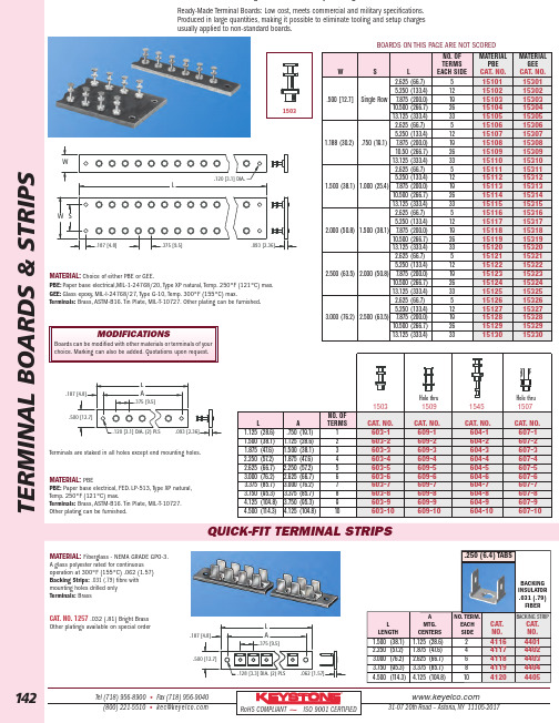
T E R M I N A L B O A R D S &S T R I P S142Tel (718)956-8900•Fax (718)956-9040(800)221-5510•kec@31-0720th Road –Astoria,NY 11105-2017RoHS COMPLIANT ~ISO 9001CERTIFIED®QUICK-FIT TERMINAL STRIPSA.375[9.5].187[4.8]L .500[12.7].128[3.3] DIA .(2)PLS.062 [1.57]BACKING INSULATOR .031(.79)FIBERA NO.TERM.BACKING STRIPL MTG.EACH CAT.CAT.LENGTHCENTERS SIDENO.NO.1.500(38.1) 1.125(28.6)2411644012.250(57.2) 1.875(47.6)4411744023.000(76.2) 2.625(66.7)6411844033.750(95.3) 3.375(85.7)8411944044.500(114.3) 4.125(104.8)1041204405MATERIAL:Fiberglass -NEMA GRADE GPO-3.A glass polyester rated for continuous operation at 300°F (155°C).062(1.57)Backing Strips:.031(.79)fibre with mounting holes drilled only Terminals:BrassCAT.NO.1257.032(.81)Bright Brass Other platings available on special orderNO.OF L A TERMS CAT.NO.CAT.NO.CAT.NO.CAT.NO.1.125(28.6).750(19.1)1603-1609-1604-1607-11.500(38.1) 1.125(28.6)2603-2609-2604-2607-21.875(47.6) 1.500(38.1)3603-3609-3604-3607-32.250(57.2) 1.875(47.6)4603-4609-4604-4607-42.625(66.7) 2.250(57.2)5603-5609-5604-5607-53.000(76.2) 2.625(66.7)6603-6609-6604-6607-63.375(85.7) 3.000(76.2)7603-7609-7604-7607-73.750(95.3) 3.375(85.7)8603-8609-8604-8607-84.125(104.8) 3.750(95.3)9603-9609-9604-9607-94.500(114.3)4.125(104.8)10603-10609-10604-10607-10NO.OF MATERIAL MATERIAL TERMS PBEGEE W S L EACH SIDE CAT.NO.CAT.NO.2.625(66.7)515101153015.250(133.4)121510215302.500[12.7]Single Row 7.875(200.0)19151031530310.500(266.7)26151041530413.125(333.4)3315105153052.625(66.7)515106153065.250(133.4)1215107153071.188(30.2).750(19.1)7.875(200.0)19151081530810.50(266.7)26151091530913.125(333.4)3315110153102.625(66.7)515111153115.250(133.4)1215112153121.500(38.1)1.000(25.4)7.875(200.0)19151131531310.500(266.7)26151141531413.125(333.4)3315115153152.625(66.7)515116153165.250(133.4)1215117153172.000(50.8)1.500(38.1)7.875(200.0)19151181531810.500(266.7)26151191531913.125(333.4)3315120153202.625(66.7)515121153215.250(133.4)1215122153222.500(63.5)2.000(50.8)7.875(200.0)19151231532310.500(266.7)26151241532413.125(333.4)3315125153252.625(66.7)515126153265.250(133.4)1215127153273.000(76.2)2.500(63.5)7.875(200.0)19151281532810.500(266.7)26151291532913.125(333.4)331513015330BOARDS ON THIS PAGE ARE NOT SCOREDReady-Made Terminal Boards:Low cost,meets commercial and military specifications.Produced in large quantities,making it possible to eliminate tooling and setup charges usually applied to non-standard boards.Terminals are staked in all holes except end mounting holes.Hole thru 1503W S.375[9.5].187[4.8].093 [2.36].120[3.1]DIA.WLA.375[9.5].187[4.8]L .500[12.7].120[3.1]DIA .(2)PLS.093[2.36]Hole thru1503150915451507MATERIAL:Choice of either PBE or GEE.PBE:Paper base electrical,MIL-1-24768/20,Type XP natural,Temp.250°F (121°C)max.GEE:Glass epoxy,MIL-I-24768/27,Type G-10,Temp.300ºF (155°C)max.Terminals:Brass,ASTM-B16.Tin Plate,MIL-T-10727.Other plating can be furnished .MATERIAL:PBEPBE:Paper base electrical,FED.LP-513,Type XP natural,Temp.250°F (121°C)max.Terminals:Brass,ASTM-B16.Tin Plate,MIL-T-10727.Other plating can be furnished .MODIFICATIONSBoards can be modified with other materials or terminals of your choice.Marking can also be added.Quotations upon request..250(6.4)TABS分销商库存信息:KEYSTONE-ELECTRONICS405640574058 40594060603-1 609-1604-1607-1 603-2609-2607-2 603-3607-3604-2 609-3603-4609-4 607-415101603-5 609-5604-3609-6 603-615301607-5 609-7603-7607-6 604-4609-8603-8 609-9603-9607-8 609-10604-5603-10 607-91510615102 15111604-6607-10 607-71511615121 153021********* 604-715126604-8 1531615103604-9 1532115326604-10 153031********* 151041511715122 153071********* 153121531715105 153221532715108 153051511315118 151231512815308 153181531315109 151141511915323 153091512415328 151291********* 153141512015319 151251513015324 153291********* 153201532515330。
AP4060规格书
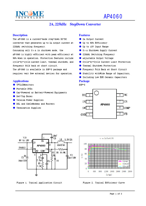
2A, 225kHz StepDown ConverterFigure 1. Typical Application Circuit Figure 2. Typical Efficiency CurveDescription The AP4060 is a current-mode step-down DC-DC converter that generates up to 2A output current at 225kHz switching frequency. Consuming only 8μA in shutdown mode, the AP4060 is highly efficient with peak efficiency at 95% when in operation. Protection features include cycle-by-cycle current limit, thermal shutdown, and frequency fold back at short circuit. The AP4060 is available in SOP-8 package and requires very few external devices for operation. Applications ● TFTLCDMonitors ● Portable DVDs ● Car-Powered or Battery-Powered Equipments ● Set-Top Boxes ● Telecom Power Supplies ● DSL and CableModems and Routers ● Termination Supplies Features ● 2A Output Current ● Up to 95% Efficiency ● Up to 18V Input Range ● 8μA Shutdown Supply Current ● 225kHz Switching Frequency ● Adjustable Output Voltage ● Cycle-by-Cycle Current Limit Protection ● Thermal Shutdown Protection ● Frequency Fold Back at Short Circuit ● Stability withWide Range of Capacitors, ● Including Low ESR Ceramic Capacitors PackageSOP-8AbsoluteMaximumRatings(Note: Do not exceed these limits to prevent damage to the device. Exposure to absolute maximum rating conditions for long periods may affect device reliability.)PARAMETER VALUE UNITIN Supply Voltage -0.3 to 18VSW Voltage-1 to V IN + 1VBS Voltage V SW–0.3 to V SW+ 8VEN, FB, COMP Voltage-0.3 to 6VContinuous SW Current Internally limited AJunction to Ambient Thermal Resistance (θJA)105°C/WOperating Junction Temperature-40 to 150°CStorage Temperature-55 to 1°CLead Temperature (Soldering, 10 sec)300°CElectricalCharacteristics(V IN = 12V, T J = 25 C unless otherwise specified)PARAMETER SYMBO TEST CONDITIONS MIN TYP MAX UNIT Input Voltage VIN V OUT = 5V, I LOAD = 1A 6 18 V Input UVLO 4.0 V Feedback Voltage VFB V COMP= 1.5V 1.196 1.22 1.244VHigh-Side Switch On Resistance RONH 0.3 ΩLow-Side Switch On Resistance RONL 8 ΩSW Leakage V EN = 0 0 10 µA Current Limit ILIM 3 3.3 ACOMP to Current Limit Transconductance GCOMP1.8 A/VError Amplifier Transconductance GEA ∆I COMP= ±10µA 550 µA/V Error Amplifier DC Gain AVEA 4000V/V Switching Frequency fSW 190 225240kHz Short Circuit Switching Frequency V FB= 050kHz Maximum Duty Cycle DMAX V FB= 1.1V92% Minimum Duty Cycle V FB= 1.3V0% Enable Threshold Voltage Hysteresis = 0.2V0.51 1.3V Enable Pull Up Current Pin pulled up to 4.5V typicallywhen left unconnected1µA Supply Current in Shutdown V EN = 0 8 20 µA IC Supply Current in Operation V EN =3V, V FB=1.3V 0.7 mA Soft-start Period 10 ms Thermal Shutdown 150 °CFigure 3. Functional Block DiagramFunctional DescriptionAs seen in Figure 2, Functional Block Diagram,the AP4060 is a current mode pulse widthmodulation (PWM) converter. The converter operatesas follows:A switching cycle starts when the rising edgeof the Oscillator clock output causes the High- Side Power Switch to turn on and the Low-Side Power Switch to turn off. With the SW side of the inductor now connected to IN, the inductor current ramps up to store energy in the its magnetic field. The inductor current level is measured by the Current Sense Amplifier and added to the Oscillator ramp signal. If the resulting summation is higher than the COMP voltage, the output of the PWM Comparator goes high.Whenthis happens or when Oscillatorclock output goes low, the High-Side Power Switch turns off and the Low-Side Power Switch turns on. At this point, the SW side of the inductor swings to a diode voltage below ground, causing the inductor current to decrease and magnetic energy to be transferred to output. This state continues until the cycle starts again.The High-Side Power Switch is driven by logicusing BS bootstrap pin as the positive rail. This pin is charged to V SW + 6V when the Low-Side Power Switch turns on.The COMP voltage is the integration of the error between FB input and the internal 1.293Vreference. If FB is lower than the reference voltage, COMP tends to go higher to increase current to the output. Current limit happens when COMP reachesits maximum clamp value of 2.55V.The Oscillator normally switches at 225kHz. However, if FB voltage is less than 0.7V, then the switching frequency decreases until it reaches a minimum of 50kHz at V FB = 0.5V.SHUTDOWN CONTROLThe AP4060 has an enable input EN for turning theIC on or off. When EN is less than 0.7V, the IC is in 8μA low current shutdown mode. When EN is higher than 1.3V, the IC is in normal operation mode. EN is internally pulled up with a 1μA current source and can be left unconnected for always-on operation. Note that EN is a low voltage input with a maximum voltage of 6V; it should never be directly connected to IN. THERMAL SHUTDOWNThe AP4060 automatically turns off when itsjunction temperature exceeds 150°C.Application InformationOUTPUT VOLTAGE SETTINGFigure 3. Output Voltage SettingFigure 3 shows the connections for setting theoutput voltage. Select the proper ratio of the twofeedback resistors R FB1 and R FB2 based on theoutput voltage. Typically, use R FB2≈10kΩ anddetermine R FB1 from the output voltage:INPUT CAPACITORThe input capacitor needs to be carefully selectedto maintain sufficiently low ripple at the supplyinputof the converter. A low ESR capacitor is highlyrecommended. Since large current flows in and out ofthis capacitor during switching, its ESR also affectsefficiency.The input capacitance needs to be higher than10μF. The best choice is the ceramic type; however,low ESR tantalum or electrolytic types may also beused provided that the RMS ripple current rating ishigher than 50% of the output current. The inputcapacitor should be placed close to the IN and Gpins of the IC, with shortest traces possible. In thecase of tantalum or electrolytic types, they can befurther away if a small parallel 0.1μF ceramiccapacitor is placed right next to the IC.OUTPUT CAPACITORThe output capacitor also needs to have low ESRto keep low output voltage ripple. The outputripple voltage is:INDUCTOR SELECTIONThe inductor maintains a continuous current tothe output load. This inductor current has a ripplethat is dependent on the inductance value: higherinductance reduces the peak-to-peak ripplecurrent. The trade off for high inductance value isthe increase in inductor core size and seriesresistance, and the reduction in current handlingcapability. In general, select an inductance value Lbased on ripple current requirement:where V IN is the input voltage, V OUT is the outputvoltage, f SW is the switching frequency, I OUTMAX is themaximum output current, and K RIPPLE is the ripplefactor. Typically, choose K RIPPLE= 30%to correspond tothe peak-to-peak ripple current being 30% of themaximum output current.With this inductor value (Table 1), the peakinductor current is I OUT•(1+K RIPPLE / 2). Make surethat this peak inductor current is less that the 3Acurrent limit. Finally, select the inductor core sizeso that it does not saturate at 3A.Table 1. Typical Inductor ValuesV OUT 1.5V 1.8V 2.5V 3.3V 5VL 10μH10μH15μH22μH33μHwhere I OUTMAX is the maximum output current,K RIPPLE is the ripple factor, R ESR is the ESRresistance of the output capacitor, f SW is theswitching frequency,L in the inductor value, C OUTis the output capacitance.In the case of ceramicoutput capacitors, R ESR is very small and does notcontribute to the ripple. Therefore, a lowercapacitance value can be used for ceramic type.In the case of tantalum or electrolytic type,the ripple is dominated by R ESR multiplied by theripple current. In that case, the output capacitorischosen to have sufficiently low ESR.For ceramic output type, typically choose acapacitance of about 22μF. For tantalum orelectrolytic type, choose a capacitor with lessthan 50mΩ ESR.RECTIFIER DIODEUse a Schottky diode as the rectifier toconduct current when the High-Side Power Switchis off. The Schottky diode must have currentrating input voltage.STABILITY COMPENSATIONFigure 4. Stability CompensationThe dominant pole P1 is due to CCOMPThe second pole P2 is the output pole:The first zero Z1 is due to R COMP and C COMP:And finally, the third pole is due to R COMP and C COMP2 (if C COMP2 is used):Follow the following steps to compensate the IC:STEP 1. Set the cross over frequency at 1/5 of the switching frequency via R COMP :but limit R COMP to 15kΩ maximum.STEP 2. Set the zero f Z1 at 1/4 of the cross over frequency. If R COMP is less than 15kΩ, the equation for C COMP is: The feedback system of the IC is stabilized by the components at COMP pin, as shown in Figure 4.The DC loop gain of the system is determined by the following equation:If R COMP is limited to 15kΩ, then the actual cross over frequency is 3.4 / (V OUT C OUT).Therefore:STEP 3. If the output capacitor’s ESR is high enoughto cause a zero at lower than 4 times the cross over frequency, an additional compensationcapacitor C COMP2 is required. The condition for using C COMP2 is:And the proper value for Ccomp2 is:Though C COMP2 is unnecessary when the output capacitor has sufficiently low ESR, a small value C COMP2 such as 100pF may improve stability against PCB layout parasitic effects.Table 2. Typical Compensation for Different Output Voltages and Output Capacitors V outC outR compC compC comp22.5V 22µF Ceramic 5.6 k Ω 6.8 nF None3.3V 22µF Ceramic 7.2 k Ω 2.2 nF None 5V 22µF Ceramic 10k Ω 1.5nF None 2.5V 47µF SP Cap 15k Ω1.5nFNone 3.3V 47µF SP Cap 15K Ω 1.8nF None 5V 47µF SP Cap 15k Ω 2.7nF None 2.5V470µF/6.3V/30m Ω 15k Ω 15nF 1nF 3.3V 470µF/6.3V/30m Ω 15k Ω 22nF 1nF 5V 470µF/10V/30m Ω15k Ω27nFNoneFigure 4 shows a sample AP4060 application circuit generating 2.5V/2A output.Figure 4. AP4060 2.5V/2A Output ApplicationTypical Performence CharacteristicsOrdering InformationPART NUMBER MARK1TEMPERATURERANGEPACKAGE PINSAP40602920YYWW1-40℃to 85℃SOP-881. Y= Year.W = Week.Pin ConfigurationPin DescriptionPIN NUMBERPINNAMEPIN DESCRIPTION1 BS Bootstrap. This pin acts as the positive rail for the high-side switch’s gate driver.Connect a 10nF between this pin and SW.2 IN Input Supply. Bypass this pin to G with a low ESR capacitor. See Input Capacitor inApplication Information section.3 SWSwitch Output. Connect this pin to the switching end of the inductor.4 GGround.5 FBFeedback Input. The voltage at this pin is regulated to 1.22V. Connect to the resistordivider between output and ground to set output voltage.6 COMPCompensation Pin. See Compensation Technique in Application Information section.7 ENEnable Input. When higher than 1.3V, this pin turns the IC on. When lower than 0.7V,this pin turns the IC off. Output voltage is discharged when the IC is off. This pin has asmall internal pull up current to a high level voltage when pin is not connected.8 N/CNot Connected.PackageOutlineSOP-8 PACKAGEOUTLINEAND DIMENSIONSSYMBOL DIMENSION IN MILIMETERS DIMENSION IN INCHESA 1.350 1.750 0.053 0.069A 0.100 0.250 0.004 0.010A 1.350 1.550 0.053 0.061B 0.330 0.510 0.013 0.020C 0.190 0.250 0.007 0.010D 4.780 5.000 0.188 0.197E 3.800 4.000 0.150 0.157E 5.800 6.300 0.228 0.248e 1.270 TYP 0.050 TYPL 0.400 1.270 0.016 0.0500 0 8 0 8。
HCF4060M013TR,HCF4060BEY, 规格书,Datasheet 资料
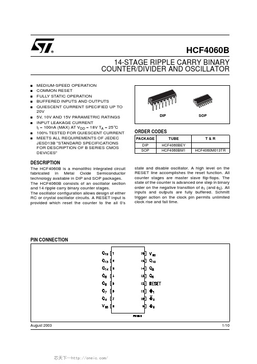
1/10August 2003s MEDIUM-SPEED OPERATION s COMMON RESETs FULLY STATIC OPERATIONs BUFFERED INPUTS AND OUTPUTSsQUIESCENT CURRENT SPECIFIED UP TO 20Vs 5V,10V AND 15V PARAMETRIC RATINGS sINPUT LEAKAGE CURRENTI I =100nA (MAX)AT V DD =18V T A =25°C s 100%TESTED FOR QUIESCENT CURRENT sMEETS ALL REQUIREMENTS OF JEDEC JESD13B "STANDARD SPECIFICATIONS FOR DESCRIPTION OF B SERIES CMOS DEVICES"DESCRIPTIONThe HCF4060B is a monolithic integrated circuit fabricated in Metal Oxide Semiconductor technology available in DIP and SOP packages.The HCF4060B consists of an oscillator section and 14ripple carry binary counter stages.The oscillator configuration allows design of either RC or crystal oscillator circuits.A RESET input is provided which reset the counter to the all 0’sstate and disable oscillator.A high level on the RESET line accomplishes the reset function.All counter stages are master slave flip-flops.The state of the counter is advanced one step in binary order on the negative transition of φ1(and φ0).All inputs and outputs are fully buffered.Schmitt trigger action on the clock pin permits unlimited clock rise and fall time.HCF4060B14-STAGE RIPPLE CARRY BINARY COUNTER/DIVIDER ANDOSCILLATORORDER CODESPACKAGE TUBE T &R DIP HCF4060BEY SOPHCF4060BM1HCF4060M013TRHCF4060B2/10INPUT EQUIVALENT CIRCUITPIN DESCRIPTIONFUNCTIONAL DIAGRAMLOGICDIAGRAMPIN No SYMBOLNAME AND FUNCTION1,2,3,4,5,6,7,13,14,15Q 12,Q 13,Q 14,Q 6,Q 5,Q 7,Q 4,Q 9,Q 8,Q 10Outputs 9,10,11Φ0,Φ0,Φ1Oscillator Input 12RESET Reset8V SS Negative Supply Volt-age16V DDPositive Supply Volt-ageHCF4060B3/10ABSOLUTE MAXIMUM RATINGSAbsolute Maximum Ratings are those values beyond which damage to the device may occur.Functional operation under these conditions is not implied.All voltage values are referred to V SS pin voltage.RECOMMENDED OPERATING CONDITIONSSymbol ParameterValue Unit V DD Supply Voltage -0.5to +22V V I DC Input Voltage -0.5to V DD +0.5V I I DC Input Current±10mA P D Power Dissipation per Package200mW Power Dissipation per Output Transistor 100mW T op Operating Temperature -55to +125°C T stgStorage Temperature-65to +150°CSymbol ParameterValue Unit V DD Supply Voltage 3to 20V V I Input Voltage0to V DD V T opOperating Temperature-55to 125°CHCF4060B4/10DC SPECIFICATIONSThe Noise Margin for both "1"and "0"level is:1V min.with V DD =5V,2V min.with V DD =10V,2.5V min.with V DD =15VSymbolParameterTest ConditionValue UnitV I (V)V O (V)|I O |(µA)V DD (V)T A =25°C -40to 85°C -55to 125°C Min.Typ.Max.Min.Max.Min.Max.I LQuiescent Current0/550.0455150µA0/10100.0410103000/15150.0420206000/20200.081001003000V OHHigh Level Output Voltage0/5<15 4.95 4.95 4.95V0/10<1109.959.959.950/15<11514.9514.9514.95V OLLow Level Output Voltage 5/0<150.050.050.05V10/0<1100.050.050.0515/0<1150.050.050.05V IHHigh Level Input Voltage 0.5/4.5<15 3.5 3.5 3.5V1/9<1107771.5/13.5<115111111V ILLow Level Input Voltage 4.5/0.5<15 1.5 1.5 1.5V9/1<11033313.5/1.5<115444I OHOutput Drive Current0/5 2.5<15-1.36-3.2-1.15-1.1mA0/5 4.6<15-0.44-1-0.36-0.360/109.5<110-1.1-2.6-0.9-0.90/1513.5<115-3.0-6.8-2.4-2.4I OLOutput Sink Current0/50.4<150.4410.360.36mA 0/100.5<110 1.1 2.60.90.90/15 1.5<115 3.06.8 2.42.4I I Input Leakage Current0/18Any Input 18±10-5±0.3±0.3±1µA C IInput CapacitanceAny Input57.5pFHCF4060B5/10DYNAMIC ELECTRICAL CHARACTERISTICS (T amb =25°C,C L =50pF,R L =200K Ω,t r =t f =20ns)(*)Typical temperature coefficient for all V DD values is 0.3%/°C,all input rise and fall times=20ns.(**)RC Oscillator applications are not recommended at supply voltages below 7V for R X <50K ΩSymbolParameterTest ConditionValue (*)UnitV DD (V)Min.Typ.Max.t TLH t THL Output Transition Time5100200ns 1050100154080t PLH t PHL Propagation Delay Time (φto Q 4out)5370740ns1015030015100200t PLH t PHL Propagation Delay Time(Q n to Q n+1)5100200ns1050100154080t WInput Pulse Width5f =100KHz 50100ns102040151530t r t fInput Pulse Rise and Fall Time5Unlimited µs1015f maxMaximum Clock Input Frequency5 3.57MHz10816151224RESET OPERATION t PHL Propagation Delay Time5180360ns10801601550100t WInput Pulse Width560120ns103060152040RC OPERATIONVariation of Frequency (Unit-to-Unit)5C X =200pF,R S =560K Ω, R X =50K Ω1821.525KHz102023261521.12427Variation of Frequency With Voltage Change (Same Unit)5to 10C X =200pF,R S =560K Ω, R X =50K Ω2KHz10to 151R X5C X =10µF 20M Ω10C X =50µF 2015C X =10µF 10C X5R X =500K Ω1000µF 10R X =300K Ω5015R X =300K Ω50Maximum Oscillator Frequency (**)10R X =5K Ω, C X =15pF530650810KHz 15690800940HCF4060B6/10DETAIL OF TYPICAL FLIP-FLOP STAGETYPICAL RC OSCILLATOR CIRCUITTYPICAL CRYSTAL OSCILLATORCIRCUITHCF4060BInformation furnished is believed to be accurate and reliable. However, STMicroelectronics assumes no responsibility for the consequences of use of such information nor for any infringement of patents or other rights of third parties which may result from its use. No license is granted by implication or otherwise under any patent or patent rights of STMicroelectronics. Specifications mentioned in this publication are subject to change without notice. This publication supersedes and replaces all information previously supplied. STMicroelectronics products are not authorized for use as critical components in life support devices or systems without express written approval of STMicroelectronics.© The ST logo is a registered trademark of STMicroelectronics© 2003 STMicroelectronics - Printed in Italy - All Rights ReservedSTMicroelectronics GROUP OF COMPANIESAustralia - Brazil - Canada - China - Finland - France - Germany - Hong Kong - India - Israel - Italy - Japan - Malaysia - Malta - Morocco Singapore - Spain - Sweden - Switzerland - United Kingdom - United States.© 10/10。
TC4426MJA;TC4427MJA;TC4428MJA;中文规格书,Datasheet资料
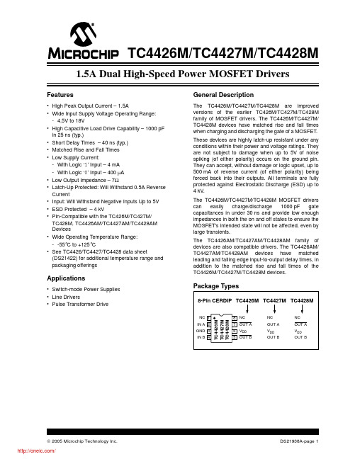
• Switch-mode Power Supplies • Line Drivers • Pulse Transformer Drive
General Description
The TC4426M/TC4427M/TC4428M are improved versions of the earlier TC426M/TC427M/TC428M family of MOSFET drivers. The TC4426M/TC4427M/ TC4428M devices have matched rise and fall times when charging and discharging the gate of a MOSFET.
Package Types
8-Pin CERDIP TC4426M TC4427M TC4428M
NC 1 IN A 2 GND 3 IN B 4
8 NC 7 OUT A 6 VDD 5 OUT B
NC
OUT A VDD OUT B
NC
OUT A VDD OUT B
TC4426M TC4427M TC4428M
1.5A Dual High-Speed Power MOSFET Drivers
Featuresቤተ መጻሕፍቲ ባይዱ
• High Peak Output Current – 1.5A • Wide Input Supply Voltage Operating Range:
- 4.5V to 18V • High Capacitive Load Drive Capability – 1000 pF
© 2005 Microchip Technology Inc.
HEF4060BD中文资料

HEF4060BD中文资料DATA SHEETProduct speci?cationFile under Integrated Circuits, IC04January 1995INTEGRATED CIRCUITSHEF4060B MSI14-stage ripple-carry binary counter/divider and oscillator For a complete data sheet, please also download:The IC04 LOCMOS HE4000B Logic Family Specifications HEF, HEC ?The IC04 LOCMOS HE4000B LogicPackage Outlines/Information HEF, HECPhilips Semiconductors Product speci?cation14-stage ripple-carry binary counter/divider and oscillator HEF4060BMSIDESCRIPTIONThe HEF4060B is a 14-stage ripple-carry binarycounter/divider and oscillator with three oscillator terminals (RS, R TC and C TC ), ten buffered outputs (O 3to O 9and O 11to O 13)and an overriding asynchronous master reset input (MR). The oscillator configuration allows design of either RC or crystal oscillator circuits. The oscillator maybe replaced by an external clock signal at input RS. The counter advances on the negative-going transition of RS.A HIGH level on MR resets the counter (O 3to O 9and O 11to O 13= LOW), independent of other input conditions.Schmitt-trigger action in the clock input makes the circuit highly tolerant to slower clock rise and fall times.Fig.1 Functional diagram.Fig.2 Pinning diagram.PINNING FAMILY DATA, I DD LIMITS category MSI See Family SpecificationsMR master resetRS clock input/oscillator pin R TC oscillator pinC TC external capacitor connection O 3to O 9counter outputsO 11to O 13HEF4060BP(N):16-lead DIL; plastic (SOT38-1)HEF4060BD(F): 16-lead DIL; ceramic (cerdip)(SOT74)HEF4060BT(D):16-lead SO; plastic (SOT109-1)(): Package Designator North AmericaPhilips Semiconductors Product speci?cation14-stage ripple-carry binary counter/dividerand oscillator HEF4060B MSIFig.3 Logic diagram.and oscillator MSIAC CHARACTERISTICSV SS=0 V; T amb=25°C;C L= 50 pF; input transition times≤20 nsV DD V SYMBOL MIN.TYP.MAX.TYPICAL EXTRAPOLATIONFORMULAPropagation delaysRS→O35210420ns183ns+(0,55 ns/pF) C L HIGH to LOW10t PHL80160ns69ns+(0,23 ns/pF) C L1550100ns42ns+(0,16 ns/pF) C L5210420ns183ns+(0,55 ns/pF) C L LOW to HIGH10t PLH80160ns69ns+(0,23 ns/pF) C L1550100ns42ns+(0,16 ns/pF) C L O n→O n+152550nsHIGH to LOW10t PHL1020ns15612ns52550nsLOW to HIGH10t PLH1020ns15612nsMR→O n5100200ns73ns+(0,55 ns/pF) C L HIGH to LOW10t PHL4080ns29ns+(0,23 ns/pF) C L153060ns22ns+(0,16 ns/pF) C L Output transition560120ns10ns+(1,0 ns/pF) C L times10t THL3060ns9ns+(0,42 ns/pF) C L HIGH to LOW152040ns6ns+(0,28 ns/pF) C L560120ns10ns+(1,0 ns/pF) C L LOW to HIGH10t TLH3060ns9ns+(0,42 ns/pF) C L152040ns6ns+(0,28 ns/pF) C L Minimum clock pulse512060nswidth input RS10t WRSH5025nsHIGH153015nsMinimum MR pulse55025nswidth; HIGH10t WMRH3015ns152010nsRecovery time516080nsfor MR10t RMR8040ns156030nsMaximum clock pulse548MHzfrequency input RS10f max1020MHz151530MHzand oscillatorMSIAC CHARACTERISTICSV SS =0 V; T amb =25°C; input transition times ≤20 nsNotes 1.where:f i =input frequency (MHz)f o =output frequency (MHz)C L =load capacitance (pF)V DD =supply voltage (V)C t =timing capacitance (pF)f osc =oscillator frequency (MHz)RC oscillatorV DD VTYPICAL FORMULA FOR P (μW)(1)Dynamic power dissipation5700f i +f o C L V DD 2per package 103300f i +f o C L V DD 2(P)158900f i+f o C L V DD 2Total power dissipation5700f osc +f o C L V DD 2+2C t V DD 2f osc +690V DD when using the 103300f osc +f o C L V DD 2+2C t V DD 2f osc + 6900V DDon-chip oscillator (P)158900f osc +f o C L V DD 2+2C t V DD 2f osc +22000V DDFig.4 External component connection for RC oscillator.Typical formula for oscillator frequency:f osc 12,3R t C t××--------------------------------=and oscillator MSITiming component limitationsThe oscillator frequency is mainly determined byR t C t,provided R t<<="" p="" r2c2<of R2 is to minimize the influence of the forward voltageacross the input protection diodes on the frequency. Thestray capacitance C2 should be kept as small as possible.In consideration of accuracy, C t must be larger than theinherent stray capacitance. R t must be larger than theLOCMOS ‘ON’ resistance in series with it, which typically is 500?at V DD=5 V, 300?at V DD=10 V and 200?atV DD=15 V.The recommended values for these components tomaintain agreement with the typical oscillation formula are:C t≥100 pF, up to any practical value,10 k?≤R t≤1 M?.Typical crystal oscillator circuitIn Fig.5, R2 is the power limiting resistor. For starting andmaintaining oscillation a minimum transconductance isnecessary.Fig.5External component connection for crystaloscillator.Fig.6Test set-up for measuring forward transconductance g fs=di o/dv i at v o is constant (see also graph Fig.7);MR = LOW.and oscillator MSIFig.7Typical forward transconductance g fs as a function of the supply voltage at T amb = 25°C.A: averageB: average + 2 s,C: average ?2 s, where ‘s’ is the observed standard deviation.Fig.8RC oscillator frequency as a function of R t and C t at V DD = 5 to 15 V; T amb =25°C.C t curve at R t =100 k ?; R2 = 470 k ?.R t curve at C t =1 nF; R2 = 5 R t .Fig.9Oscillator frequency deviation (?f osc )as a function of ambient temperature; referenced at: f osc at T amb =25°C and V DD =10 V.___R t =100 k ?; C t =1 nF; R2=0.---R t =100 k ?;C t =1 nF; R2= 300 k ?.。
NSR0620P2T5G;中文规格书,Datasheet资料
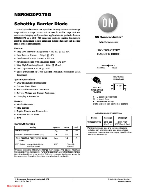
NSR0620P2T5GSchottky Barrier DiodeSchottky barrier diodes are optimized for very low forward voltage drop and low leakage current and are used in a wide range of dc−dc converter, clamping and protection applications in portable devices. NSR0620P2 in a SOD−923 miniature package enables designers to meet the challenging task of achieving higher efficiency and meeting reduced space requirements.Features•Very Low Forward V oltage Drop − 350 mV @ 100 mA •Low Reverse Current − 2.0 m A @ 10 V•Continuous Forward Current − 500 mA•Power Dissipation with Minimum Trace − 190 mW•Very High Switching Speed − 4.0 ns @ 10 mA•Low Capacitance − 12 pF @ 1.0 V•These Devices are Pb−Free, Halogen Free/BFR Free and are RoHS CompliantTypical Applications•LCD and Keypad Backlighting•Camera Photo Flash•Buck and Boost dc−dc Converters•Reverse V oltage and Current Protection•Clamping & ProtectionMarkets•Mobile Handsets•MP3 Players•Digital Camera and Camcorders•Notebook PCs & PDAs•GPSMAXIMUM RATINGSRating Symbol Value Unit Reverse Voltage VR20VdcForward Continuous Current (DC)I F500mA Non−Repetitive Peak Forward SurgeCurrentI FSM 1.0AESD Rating:Human Body ModelMachine Model ESD Class 3BClass CStresses exceeding Maximum Ratings may damage the device. Maximum Ratings are stress ratings only. Functional operation above the Recommended Operating Conditions is not implied. Extended exposure to stresses above the Recommended Operating Conditions may affect device reliability.20 V SCHOTTKYBARRIER DIODE12Device Package Shipping†ORDERING INFORMATIONNSR0620P2T5G SOD−923(Pb−Free)2 mm Pitch8000/T ape & Reel †For information on tape and reel specifications, including part orientation and tape sizes, please refer to our Tape and Reel Packaging Specifications Brochure, BRD8011/D.SOD−923CASE 514ABPLASTICF= Specific Device CodeM=Month CodeG= Pb−Free Package(Note: Microdot may be in either location)MARKINGDIAGRAMTHERMAL CHARACTERISTICSCharacteristicSymbol Max Unit Thermal ResistanceJunction −to −Ambient (Note 1)Total Power Dissipation @ T A = 25°C R q JA P D 520190°C/W mW Thermal ResistanceJunction −to −Ambient (Note 2)Total Power Dissipation @ T A = 25°C R q JA P D 175570°C/W mW Junction and Storage Temperature RangeT J , T stg−55 to +125°C1.Mounted onto a 4 in square FR −4 board 10 mm sq. 1 oz. Cu 0.06” thick single −sided. Operating to steady state.2.Mounted onto a 4 in square FR −4 board 1 in sq. 1 oz. Cu 0.06” thick single −sided. Operating to steady state.ELECTRICAL CHARACTERISTICS (T A = 25°C unless otherwise noted)CharacteristicSymbol MinTyp Max Unit Reverse Leakage (V R = 10 V)(V R = 20 V)I R2.09.010m AForward Voltage (I F = 10 mA)(I F = 100 mA)(I F = 500 mA)V F270350480310390520mVTotal Capacitance(V R = 1.0 V, f = 1 MHz)CT12pF Reverse Recovery Time(I F = I R = 10 mA, I R= 1.0 mA)trr4.0nsF ) of 10 mA.2.Pulse Generator Output is adjusted for a Peak Reverse Recovery Current I RM of 10 mA.3.Pulse Generator transition time << t rr .4.I R(REC) is measured at 1 mA. Typically 0.1 X I RM or 0.25 X I RM .5.t p » t rrt 10%90%I FI RMOutput Pulse(I F = I RM = 10 mA; measuredat i R(REC) = 1 mA)Pulse GeneratorOutputFigure 1. Recovery Time Equivalent Test CircuitV R0.11101001000V F , FORWARD VOLTAGE (V)Figure 2. I F , F O R W A R D C U R R E N T (m A )V R , REVERSE VOLTAGE (V)Figure 3.I R , R E V E R S E C U R R E N T (m A)0.00010.0010.010.111010010001000024681012141618202202468101214161820V R , REVERSE VOLTAGE (V)Figure 4.C t , T O T A L C A P A C I T A N C E (p F )PACKAGE DIMENSIONSSOD −923CASE 514AB ISSUE CNOTES:1.DIMENSIONING AND TOLERANCING PER ASME Y14.5M, 1994.2.CONTROLLING DIMENSION: MILLIMETERS.3.MAXIMUM LEAD THICKNESS INCLUDES LEAD FINISH. MINIMUM LEAD THICKNESS IS THE MINIMUM THICKNESS OF BASE MATERIAL.4.DIMENSIONS D AND E DO NOT INCLUDE MOLD FLASH, PROTRUSIONS, OR GATE BURRS.DIM MIN NOM MAX MILLIMETERS A 0.340.370.40b 0.150.200.25c 0.070.120.17D 0.750.800.85E 0.550.600.650.95 1.00 1.05L 0.19 REF H E 0.0130.0150.0160.0060.0080.0100.0030.0050.0070.0300.0310.0330.0220.0240.0260.0370.0390.0410.007 REFMIN NOM MAX INCHEScADIMENSIONS: MILLIMETERS*For additional information on our Pb −Free strategy and soldering details, please download the ON Semiconductor Soldering and Mounting Techniques Reference Manual, SOLDERRM/D.SOLDERING FOOTPRINT*See Application Note AND8455/D for more mounting details 2X2XOUTLINEb 2X0.08X YTOP VIEW2XBOTTOM VIEWLL20.050.100.150.0020.0040.006ON Semiconductor and are registered trademarks of Semiconductor Components Industries, LLC (SCILLC). SCILLC reserves the right to make changes without further notice to any products herein. SCILLC makes no warranty, representation or guarantee regarding the suitability of its products for any particular purpose, nor does SCILLC assume any liability arising out of the application or use of any product or circuit, and specifically disclaims any and all liability, including without limitation special, consequential or incidental damages.“Typical” parameters which may be provided in SCILLC data sheets and/or specifications can and do vary in different applications and actual performance may vary over time. All operating parameters, including “Typicals” must be validated for each customer application by customer’s technical experts. SCILLC does not convey any license under its patent rights nor the rights of others. SCILLC products are not designed, intended, or authorized for use as components in systems intended for surgical implant into the body, or other applications intended to support or sustain life, or for any other application in which the failure of the SCILLC product could create a situation where personal injury or death may occur. Should Buyer purchase or use SCILLC products for any such unintended or unauthorized application, Buyer shall indemnify and hold SCILLC and its officers, employees, subsidiaries, affiliates,and distributors harmless against all claims, costs, damages, and expenses, and reasonable attorney fees arising out of, directly or indirectly, any claim of personal injury or death associated with such unintended or unauthorized use, even if such claim alleges that SCILLC was negligent regarding the design or manufacture of the part. SCILLC is an Equal Opportunity/Affirmative Action Employer. This literature is subject to all applicable copyright laws and is not for resale in any manner.PUBLICATION ORDERING INFORMATION分销商库存信息: ONSEMINSR0620P2T5G。
- 1、下载文档前请自行甄别文档内容的完整性,平台不提供额外的编辑、内容补充、找答案等附加服务。
- 2、"仅部分预览"的文档,不可在线预览部分如存在完整性等问题,可反馈申请退款(可完整预览的文档不适用该条件!)。
- 3、如文档侵犯您的权益,请联系客服反馈,我们会尽快为您处理(人工客服工作时间:9:00-18:30)。
Notes: 1. θ1/2 is the angle from optical centerline where the luminous intensity is 1/2 of the optical peak value. 2. Luminous intensity/ luminous Flux: +/-15%.
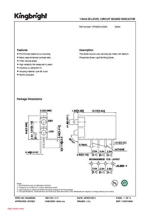
1.8mm BI-LEVEL CIRCUIT BOARD INDICATOR
Part Number: WP4060VH/2YD Yellow
Features
z Pre-trimmed leads for pc mounting. z Black case enhances contrast ratio. z Wide viewing angle. z High reliability life measured in years. z Housing UL rating:94V-0. z Housing material: type 66 nylon. z RoHS compliant.
SPEC NO: DSAE9385 APPROVED: WYNEC
REV NO: V.10 CHECKED: Allen Liu
DATE: APR/07/2011 DRAWN: J.Yu
PAGE: 1 OF 5 ERP: 1102013561
/
Selection Guide
Yellow
WP4060VH/2YD
SPEC NO: DSAE9385 APPROVED: WYNEC
REV NO: V.10 CHECKED: Allen Liu
DATE: APR/07/2011 DRAWN: J.Yu
PAGE: 3 OF 5 ERP: 1102013561
/
Notes: 1. 1/10 Duty Cycle, 0.1ms Pulse Width. 2. 2mm below package base. 3. 5mm below package base.
Yellow 75 30 140 5 -40°C To +85°C 260°C For 3 Seconds 260°C For 5 Seconds
Notes: 1.Wavelength: +/-1nm. 2. Forward Voltage: +/-0.1V.
Absolute Maximum Ratings at TA=25°C
Parameter Power dissipation DC Forward Current Peak Forward Current [1] Reverse Voltage Operating/Storage Temperature Lead Solder Temperature [2] Lead Solder Temperature [3]
Notes: 1. All dimensions are in millimeters (inches). 2. Tolerance is ±0.25(0.01") unless otherwise noted. 3. Lead spacing is measured where the leads emerge from the package. 4. The specifications, characteristics and technical data described in the datasheet are subject to change without prior notice.
Description
The Yellow source color devices are made with Gallium Arsenide Phosphide on Gallium Phosphide Yellow Light Emitting Diode.
Package Dimensions
Electrical / Optical Characteristics at TA=25°C
Symbol λpeak λD [1] Δλ1/2 C VF [2] IR Parameter Peak Wavelength Dominant Wavelength Spectral Line Half-width Capacitance Forward Voltage Reverse Current Device Yellow Yellow Yellow Yellow Yellow Yellow Typ. 590 588 35 20 2.1 2.5 10 Max. Units nm nm nm pF V uA Test Conditions IF=20mA IF=20mA IF=20mA VF=0V;f=1MHz IF=20mA VR = 5V
Units mW mA mA V
SPEC NO: DSAE9385 APPROVED: WYNEC
REV NO: V.10 CHECKED: Allen Liu
DATE: APR/07/2011 DRAWN: J.Yu
PAGE: 2 OF 5 ERP: 1102013561
/
/
SPห้องสมุดไป่ตู้C NO: DSAE9385 APPROVED: WYNEC
REV NO: V.10 CHECKED: Allen Liu
DATE: APR/07/2011 DRAWN: J.Yu
PAGE: 5 OF 5 ERP: 1102013561
/
PACKING & LABEL SPECIFICATIONS
WP4060VH/2YD
SPEC NO: DSAE9385 APPROVED: WYNEC
REV NO: V.10 CHECKED: Allen Liu
DATE: APR/07/2011 DRAWN: J.Yu
PAGE: 4 OF 5 ERP: 1102013561
分销商库存信息:
KINGBRIGHT WP4060VH/2YD