MA3J745中文资料
MMA7455角速度模块简介

MMA7455 角速度模块简介
一、MMA7455 角速度模块简介
MMA745 是一款数字输出(I2C/SPI)、低功耗、紧凑型电容式微机械加速度计,具有信号调理、低通滤波器、温度补偿、自测、可配置通过中断引脚(INT1 或INT2)检测0g、以及脉冲检测。
偏置和灵敏度是出厂配置,无需外部器件。
客户可使用指定的0g 寄存器和g-Select 量程选择对0g 偏置进行校准,量程可通过命令选择3 个加速度范围(2g/4g/8g)。
MMA745xL 系列具备待机模式,使它成为以电池为电源的手持式电子器件的理想选择。
MMA7455 数字三轴加速度传感器模块核心为飞思卡尔公司的
MMA7455L 数字三轴加速度传感器,该模块设计使用官方推荐设计,板卡线路经过高电磁兼容设计和优化,具有输出精确,体积小,工作可靠,各种标识清晰,扩展性好等特点。
MMA7455L 芯片安装在带DIP 插脚的印刷电路板(PCB)上,它允许客户将其集成到特定的设计应用对产品进行评估。
这样客户就能够在他们自己硬件和软件环境内灵活地评估器件。
模块参数:。
MAX4475

概述MAX4575/MAX4576/MAX4577是低电压,高静电放电(ESD)保护,双单极/单掷(SPST)模拟开关。
常关闭(NO)和常开(NC)引脚对± 15kV的ESD保护而不闭锁或损坏。
每个交换机可以处理轨到轨®模拟信号。
关断漏电流0.5nA在25 ° C。
这些适合低失真音频模拟开关应用和首选的解决方案在自动化测试设备或机械继电器开关电流所需的应用程序。
他们具有低功耗的要求(0.5μW),需要更少的电路板空间,比机械更可靠继电器。
每个设备控制的TTL / CMOS输入电压等级是双边的。
这些开关的功能保证操作+2 V至+12 V单电源供电,使他们的理想使用电池供电的应用。
电阻70Ω(最大),交换机之间的匹配,0.5Ω(典型值)单位在指定的信号范围内(2Ω典型)。
MAX4575有两个无开关,MAX4576两个NC交换机和MAX4577有一个NO和一个NC开关。
这些器件采用8引脚μMAX和SO封装。
应用电池供电系统音频和视频信号路由低电压数据采集系统采样和保持电路通信电路继电器替代品____________________________Features?NO / NC引脚的ESD保护± 15kV的(人体模型)± 15KV(IEC 1000-4-2气隙放电)± 8千伏(IEC 1000-4-2接触放电)?与MAX4541/MAX4542/MAX4543引脚兼容?保证电阻+5 V时的70Ω(最大)在+3 V,150Ω(最大)?通电阻平坦度2Ω(典型值)为+5 V在+3 V,6Ω(典型值)?电阻匹配0.5Ω(典型值)为+5 V在+3 V,0.6Ω(典型值)?保证0.5nA漏电流在TA = +25 ° C?2 V至+12 V单电源电压?TTL / CMOS逻辑兼容?低失真:0.015%?- 3dB带宽> 300MHz的?轨到轨信号范围MAX4575/MAX4576/MAX4577± 15kV ESD保护,低电压,双通道,单刀单掷,CMOS模拟开关______________________________________________________________ __马克西姆综合产品119-1762;冯0 7 / 00;对于免费样品和最新文献,参观访问www.maxim - 或电话1-800-998-8800。
MBRB745中文资料
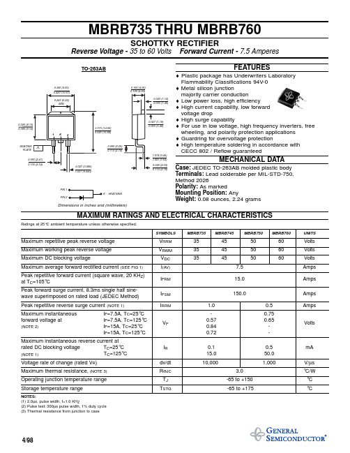
MBRB735 THRU MBRB760SCHOTTKY RECTIFIERReverse Voltage - 35 to 60 Volts Forward Current -7.5 AmperesFEATURESRatings at 25°C ambient temperature unless otherwise specified.SYMBOLS MBRB735MBRB745MBRB750MBRB760UNITS Maximum repetitive peak reverse voltage V RRM35455060Volts Maximum working peak reverse voltage V RWM35455060Volts Maximum DC blocking voltage V DC35455060Volts Maximum average forward rectified current (SEE FIG 1)I(AV)7.5Amps Peak repetitive forward current (square wave, 20 KH Z)at T C=105°CI FRM15.0Amps Peak forward surge current, 8.3ms single half sine-wave superimposed on rated load (JEDEC Method)I FSM150.0Amps Peak repetitive reverse surge current (NOTE 1)I RRM 1.00.5Amps Maximum instantaneous I F=7.5A, T C=25°C-0.75forward voltage at I F=7.5A, T C=125°CV F 0.570.65Volts(NOTE2)I F=15A, T C=25°C0.84-I F=15A, T C=125°C0.72-Maximum instantaneous reverse current atrated DC blocking voltage T C=25°C I R0.10.5mA (NOTE 1)T C=125°C15.050.0Voltage rate of change (rated V R)dv/dt10,0001,000V/µs Maximum thermal resistance,(NOTE 3)RΘJC 3.0°C/W Operating junction temperature range T J-65 to +150°C Storage temperature range T STG-65 to +175°C NOTES:(1) 2.0µs, pulse width, f=1.0 KH Z(2) Pulse test: 300µs pulse width, 1% duty cycle(3) Thermal resistance from junction to case4/98TO-263AB11010025507510012515017500.10.20.30.40.50.60.70.80.9 1.01.1 1.20.010.1110500.1110100401001,0004,0000.010.11101000.11101000501001500246810204060801000.0010.010.111050FIG. 1 - FORWARD CURRENT DERATING CURVECASE TEMPERATURE, °CA V E R A G E F O R W A R D C U R R E N T ,A M P E R E SFIG. 2 - MAXIMUM NON-REPETITIVE PEAK FORWARDSURGE CURRENTNUMBER OF CYCLES AT 60 H ZP E A K F O R W A R D S U R G E C U R R E N T ,A M P E R E SFIG. 3 - TYPICAL INSTANTANEOUS FORWARDCHARACTERISTICSFIG. 4 - TYPICAL REVERSE CHARACTERISTICSI N S T A N T A N E O U S F O R W A R D C U R R E N T , A M P E R E SI N S T A N T A N E O U S R E V E R S E C U R R E N T , M I L L I A M P E R E SINSTANTANEOUS FORWARD VOLTAGE,VOLTSPERCENT OF RATED PEAK REVERSEVOLTAGE, %FIG. 5 - TYPICAL JUNCTION CAPACITANCEJ U N C T I O N C A P A C I T A N C E , p FREVERSE VOLTAGE, VOLTST J =T J max.8.3ms SINGLE HALF SINE-WAVE (JEDEC Method)T J =75°CT J =25°CT J =25°CT J =125°CPULSE WIDTH = 300µsT J =25°C f=1.0 MHz Vsig=50mVp-pRESISTIVE OR INDUCTIVE LOADT J =125°CFIG. 6 - TYPICAL TRANSIENT THERMAL IMPEDANCEt, PULSE DURATION, sec.T R A N S I E N T T H E R M A L I M P E D A N C E , °C /WMBR735 - MBR745MBR750 & MBR760MBRB735 - MBRB745MBRB750 & MBBR760MBRB735 - MBRB745MBRB750 & MBBR760MBRB735 - MBRB745MBRB750 & MBBR760RATINGS AND CHARACTERISTIC CURVES MBRB735 THRU MBRB760。
7454中文资料

线译码器74LS154引脚,参数,及功能介绍
--------------------------------------------------------------------------------
4 线-16 线译码器 74LS154/54LS154引脚图,参数,及功能介绍
74ls154功能简介:
54/74154 为 4 线-16 线译码器,当选通端(G1、G2)均为低电平时,可将地址端(ABCD)的二进制编码在一个对应的输出端,以低电平译出。
如果将G1和G2中的一个作为数据输入端,由ABCD对输出寻址,74LS154还可作1线-16线数据分配器。
74LS154管脚图:
引脚功能介绍
A、B、C、D 译码地址输入端(低电平有效)
G1、G2 选通端(低电平有效)
0-15 输出端(低电平有效)
74ls154真值表:
推荐工作条件
74ls154电气参数
极限值
电源电压: 7V
输入电压:
工作环境温度
54154:-55~125℃
74154:0~70℃
贮存温度:-65~150℃
本文来自: 原文网址:
74ls154芯片资料
2007-08-20 20:48
74ls138译码器
74ls139 跟74ls138类似,区别在于139内部是2个独立的2-4译码器。
74ls154跟74LS138很类似,差别就在于,138是3-8译码器,154是4-16译码器。
| | | 浏览(1104) | ?(1)
上一篇:????下一篇:
最近读者:
后,您就
出现在
这里。
2018-2019-mma7455资料word版本 (10页)

本文部分内容来自网络整理,本司不为其真实性负责,如有异议或侵权请及时联系,本司将立即删除!== 本文为word格式,下载后可方便编辑和修改! ==mma7455资料篇一:MMA7455L资料汇总一、模块介绍模块的主芯片运用freescale公司的MMA7455L芯片,模块设计在主芯片的基础上加入了简单的外围电路,使用者只需做简单的改动就可以在I2C和SPI两种接口方式之间简单变换,不需另外加入电路,让使用者使用起来更加方便。
它可以实现基于运动的功能,如游戏控制、手持终端和倾斜滚动的自由落体硬盘保护等。
具有更高的封装高度、但价格却更低。
MMA7455L是一款三轴的加速度传感器,它能检测物体的运动和方向,它根据物体的运动和方向来改变输出信号的电压值。
各个轴在不运动或者失重的状态下(0g),其输出为1.65V。
如果沿着某个方向运动,或者受到重力作用,输出电压就会根据设定的灵敏度相应的改变。
然后通过I2C或者SPI的方式读取代表物体运动和方向的数值MMA7455L是一款数字输出、低功耗、紧凑型电容式微机械加速度计,具有信号调理、低通滤波器、温度补偿、自测、可配置通过中断引脚(INT1 或 INT2)检测 0g、以及脉冲检测(用于快速运动检测)等功能。
0g偏置和灵敏度是出厂配置,无需外部器件。
客户可使用指定的0g寄存器和g-Select量程选择对0g偏置进行校准,量程可通过命令选择 3个加速度范围(2g/4g/8g)。
二、模块主要参数? Z 轴自测? 低压操作:2.4V – 3.6V ? 用于偏置校准的用户指定寄存器 ? 可编程阀值中断输出? 电平检测模式运动识别(冲击、震动、自由下落) ? 脉冲检测模式单脉冲或双脉冲识别 ? 灵敏度 64 LSB/g @ 2g /8g 10位模式 ? 8位模式的可选灵敏度(±2g、±4g、±8g) ? 环境温度:-40-85摄氏度 ? 可靠的设计、高抗震性(5000g) ? 外形尺寸:3mm*5mm*1mm? 环保型产品 ? 低成本三.XYZ三轴加速度传感器的工作原理简介MMA7455L加速度传感器主要由两部分组成:G-单元和信号调理ASIC电路(见上图)。
PWS745中文资料

PWS745-1
VIN
DRIVE
GATE
TTLIN TTLOUT
GND
Oscillator
Driver
Soft Start DRIVE
GATE
PWS745-1 also allows the user to select varying levels of power, isolation voltage, mounting technology and system configuration by choosing among the several component families. For example, the PWS745-1 can directly drive the PWS740, PWS745, or PWS750 transformers. It also can drive the FETs of a PWS750 distributed power system. The operating frequency is compatible with the ISO120 family of isolation amplifiers and is capable of multi-channel synchronized operation to eliminate troublesome beat frequencies.
© 1990 Burr-Brown Corporation
PDS1-1095
®
PWS745 Printed in U.S.A. March, 1992
元器件交易网
SPECIFICATIONS
ELECTRICAL
At
V IN
=
NCR 7453号工作站Release 3.1硬件用户指南说明书

7453 hardware user ManualNCR 7453 WorkstationRelease 3.1Hardware User's GuideBD20-1424-BIssue Hv Table of ContentsChapter 1: Product OverviewIntroduction..................................................................1-1Hardware Modules......................................................1-4Processor Board......................................................1-4Features Unique to the 586 (Class 1xxx)..........1-5Features Unique to the 686 (Class 2xxx)..........1-5Features Unique to the Class 3500....................1-6Features Unique to the Series 4xxx...................1-6Graphics (other than Series 4000).....................1-7Graphics (Series 4000)........................................1-8Power Management...........................................1-9NCR 5952 Wedge DynaKey Module........................1-10NCR 5953 12.1" DynaKey..........................................1-11NCR 5962 Wedge Touch Screen................................1-13NCR 5963 Wedge Touch Screen................................1-14Operator Displays......................................................1-169" Monochrome CRT............................................1-1610" Color CRT.......................................................1-1615" Monitor...........................................................1-179.4" Monochrome LCD........................................1-17NCR 5982 LCD Display.......................................1-18NCR 15" Color Display........................................1-18NCR 5932 Keyboards.................................................1-19115-key Big Ticket Keyboard...............................1-1968-key Keyboard...................................................1-20176-key Micro Motion Keyboard........................1-21Features.......................................................................1-22viKeylock..................................................................1-23Speaker..................................................................1-23Buzzer....................................................................1-23System Status Indicator LED...............................1-24MSR (Magnetic Stripe Reader)............................1-24External Decoded Scanner Port...........................1-25Special "PC Setup" Keypad Layout for 68-keyKeyboard...............................................................1-25POS and PC Scan Mode for Micro MotionKeyboard...............................................................1-25NCR 5972 2x20 Customer Display............................1-26Features.................................................................1-26NCR 5973 International VFD Customer Display.....1-29Features.................................................................1-29NCR 5942 10.4" Customer Display...........................1-32Features.................................................................1-32Printer Options...........................................................1-337140 Printer...........................................................1-337141 Printer...........................................................1-347156 Printer...........................................................1-347158 Printer...........................................................1-357161 Printer...........................................................1-357162 Printer...........................................................1-367193 Printer...........................................................1-367194 Printer...........................................................1-37System Configuration Diagrams...............................1-38Chapter 2: Hardware InstallationIntroduction..................................................................2-1Installation Restrictions.........................................2-1Cautions..................................................................2-1viiOut-of-Box Hardware Installation..............................2-2Installing an NCR 9" Monochrome, 10" Color CRT,or 15" Monitor...............................................................2-9Installing an NCR 5952 DynaKey Module...............2-11 Installing a Checkstand-Mounted 5952DynaKey...............................................................2-12Installing a Remote DynaKey.............................2-20Installing a Wall-Mounted 5952 DynaKey.........2-24Installing an NCR 5962 Touch Screen Module........2-25 Installing a Remote 5962 Touch Screen Module2-26Wall-Mounting a 5962 Touch Screen Module....2-33Adding a 2x20 or International CustomerDisplay..................................................................2-35Installing a 5953 DynaKey.........................................2-40 Installing a Table-Top Mounted 5953 DynaKey2-42Adding a 2x20 Customer Display..................2-43Installing a Wall Mounted 5953 DynaKey.........2-45Installing a Checkstand-Mounted 5953DynaKey...............................................................2-46Installing a Weighted Base Checkstand.........2-46Installing a Checkstand Base...........................2-47Connecting the 5953 DynaKey (2xxx, 35xx).......2-50Installing a PCI LCD Board.............................2-50Connecting a 5953 DynaKey without TouchScreen................................................................2-53Connecting a 5953 DynaKey with TouchScreen................................................................2-53Connecting the 5953 DynaKey (4xxx)................2-54Installing a K148 Parallel or K156Parallel/RS-232 Port Harness..........................2-55Installing an NCR 5963 Touch Screen Module........2-57 Installing the PCI LCD Board.............................2-57viiiEquipment........................................................2-58Tools Needed....................................................2-58Connector/Strapping Identification...............2-59Cables................................................................2-60Installation in Terminal...................................2-61Connection to 5963 LCD Touch ScreenDisplay and Keyboard.....................................2-64Wall-Mounting a 5963 Touch Screen Module....2-65Installing an NCR 5972 2x20 Customer Display......2-66Installing a High-Post Table-Top Mounted 2x20Customer Display................................................2-69Installing an International VFD Customer Display.2-72Installing a Table Top Mount InternationalCustomer Display................................................2-72Installing a 16" High Post Mount InternationalCustomer Display................................................2-73Installing an NCR 5982 5" Operator Display.....2-75Installing a 5942 10.4" LCD CID................................2-77Installing a 7453-K148 on a 35xx...............................2-78Installing a Win95 Intel EtherExpress Pro AdapterDriver...........................................................................2-79Installing a Win2000 AMD Ethernet Driver.............2-81Installing an External CD-ROM Drive......................2-83Installing the Hardware.......................................2-84Installing the Drivers...........................................2-85Four-Port PCI RS-232 Board......................................2-87Hardware Installation..........................................2-87Software Installation............................................2-87Windows 95......................................................2-87Windows 98......................................................2-88Windows 2000..................................................2-88Windows NT....................................................2-89ix Default I/O Address and Interrupt Settingsfor Win95/NT...................................................2-90Default I/O Address and Interrupt Settingsfor Win98...........................................................2-91Chapter 3: SetupRunning Setup..............................................................3-1Entering Setup........................................................3-1Setting the Date and Time.....................................3-2Setting Passwords..................................................3-2Configuring a Hard Drive.....................................3-3Configuring a Flex Drive.......................................3-3Setting Memory Cache...........................................3-4Setting Memory Shadow.......................................3-4Setting Boot Options..............................................3-5Allocating Interrupts (Series 4xxx).......................3-5Resolving COM 5 and COM 6 (Series 4xxx)........3-6Restoring Factory Settings.....................................3-6 BIOS Default CMOS Values (586)...............................3-7Main Values............................................................3-7Advanced Values...................................................3-9Security Values.....................................................3-11Power Values........................................................3-11Exit Values............................................................3-13 BIOS Default CMOS Values (686).............................3-14Main Values..........................................................3-14Advanced Values.................................................3-16Security Values.....................................................3-17Power Values........................................................3-18Exit Values............................................................3-19 BIOS Default CMOS Values (3500)...........................3-21xMain Values..........................................................3-21Advanced Values.................................................3-23Security Values.....................................................3-24Power Values........................................................3-24Boot Values...........................................................3-27Exit Values............................................................3-27BIOS Default CMOS Values (4000)...........................3-28Main Values..........................................................3-28Advanced Values.................................................3-29Security Values.....................................................3-33Power Values........................................................3-33Boot Values...........................................................3-34Exit Values............................................................3-34IRQ and Port Addresses............................................3-35586 Processor Board.............................................3-35686 Processor Board.............................................3-35Series 4000 Processor Board................................3-37Memory Map (586, 3xxx 686, and 35xx 686)............3-39Memory Map (4xxx)...................................................3-40DMA Channels (586, 3xxx 686, and 35xx 686).........3-42DMA Channels (4xxx)................................................3-43Setup Tips....................................................................3-44Chapter 4: Operating System RecoveryIntroduction..................................................................4-1Prerequisites...........................................................4-1Updating Procedures.............................................4-2Completing the OS Installation (WinNT)........4-4Completing the OS Installation (Win98)..........4-5Completing the OS Installation (Win95)..........4-6Completing the OS Installation (DOS).............4-6xiGold Disk Contents......................................................4-7NCR 7452/7453-4000 Win95 OS RecoverySoftware...................................................................4-7NCR 7452/7453-4000 Win98 OS RecoverySoftware...................................................................4-8NCR 7452/7453-4000 NT Operating SystemRecovery Software..................................................4-9Chapter 5: BIOS Updating ProceduresIntroduction..................................................................5-1Disk Updating Procedures..........................................5-1Updating Procedure: 7453-10xx............................5-2Updating the PC BIOS.......................................5-2Updating the Memory Dump ROM.................5-3Updating Procedure: 7453-20xx............................5-4Updating the PC BIOS.......................................5-4Updating the Memory Dump ROM.................5-5Updating the LAN Boot ROM..........................5-6Updating Procedure: 7453-35xx............................5-7Updating the PC BIOS.......................................5-7Updating the Memory Dump ROM.................5-7Updating the LAN Boot ROM..........................5-9Updating Procedure: 7453-40xx..........................5-10Updating the PC BIOS.....................................5-10Updating the Memory Dump ROM...............5-11 CD-ROM Updating Procedure..................................5-12Prerequisites.........................................................5-12Updating Procedures...........................................5-13Appendix A: Retail Keyboard Key Layouts68-Key Keyboard.........................................................A-168-Key Keyboard Special Keypad Mode.........A-3xiiSpecial PC Setup Keypad Mode Activated(68-Key Keyboard)............................................A-4DynaKey................................................................A-5Special DynaKey Keypad Mode......................A-5Normal DynaKey Keypad Operating Mode...A-7Appendix B: RS-232 Port AssignmentOverview.......................................................................B-1686 Processor Board......................................................B-2Port Assignments in the BIOS Setup....................B-2Dual Port RS-232 Board.........................................B-3Port Assignments in the SERIALDD.DOSSetup File.................................................................B-3Port Assignments during Boot Up (MachineBIOS)........................................................................B-3Summary.................................................................B-4Touch Screen...........................................................B-410.4-Inch Touch Screen Example......................B-52x20 Customer Display..........................................B-5586 Processor Board......................................................B-7Port Assignments in the BIOS Setup....................B-7Dual Port RS-232 Board.........................................B-8Port Assignments in the SERIALDD.DOSSetup File.................................................................B-8Port Assignments during Boot Up (MachineBIOS)........................................................................B-810.4-Inch Touch Screen..........................................B-92x20 Customer Display........................................B-11CRT Configuration...............................................B-12Appendix C: Kits and CablesKits................................................................................C-1xiii Cables...........................................................................C-5IndexThis is a “Table of Contents preview” for quality assuranceThe full manual can be found at /estore/catalog/ We also offer free downloads, a free keyboard layout designer, cable diagrams, free help andsupport. : the biggest supplier of cash register and scale manuals on the net。
7457性能参数分析

随着IC芯片的日益复杂和性能的不断提高,芯片的测试速度和引脚数都不断攀升,对测试的要求也向着高速的数模混合测试方向发展。
特别是IC工作频率、封装密度的提高及SoC、ASIC高性能芯片的大量涌现,对高速、高密度、低功耗、高性价比测试系统的需求会不断提高,对被测芯片与测试仪的可靠性连接技术提出了新的挑战。
同时,随着IC测试设备的测试能力的大幅提高,测试的速度越来越快(测试速度大于500Mhz),测试精度越来越高,测试设备与被测芯片的可靠性连接也越来越显得重要。
芯片测试是集成电路产业不可或缺的一个重要环节,而测试时间和测试效能是制约集成电路产业发展的两个重要因素。
与迅速发展的设计业相比之下,我国测试业的发展却相对滞后,目前能够独立承担专业测试服务的公司寥寥无几,不能满足众多IC设计公司的验证分析和产业化测试需求,已日益成为我国集成电路产业发展的一个瓶颈。
目前,对于高端集成电路产品,主要还是送到国外去测试,国内的测试能力远远满足不了市场的需求。
公司产品的推出,将大大缩短测试时间,提高测试效能,从而达到降低测试成本,解决国内测试能力存在的问题,加速整个集成电路产业的发展。
在SoC测试方面,客户亟待能全面对应从低端到高端应用的测试解决方案,而削减影响芯片单价的测试成本更是芯片制造商要解决的课题,测试服务公司或测试设备供应商必须拿出针对各个芯片的低成本测试解决方案。
进入SoC时代以后,SoC所需的测试验证费用越来越高,IC供应商在测试上的花费接近产品总成本的三成,这也意味着将带来巨大的商机。
从上图可以看出缺乏足够的测试服务能力是大陆IC设计企业面临的主要困难之一。
全球半导体业发展到今天,集成电路测试业贯穿在集成电路设计、芯片制造、封装及集成电路应用的全过程,以前它被合并在制造业或封装业中,但随着人们对集成电路品质的重视,再加上技术、成本和知识产权保护等诸多因素,测试业目前正成为集成电路产业中一个不可或缺的独立行业。
JD745A培训(简)-GSM
12
© 2007 JDSU. All rights reserved.
用于退回到前一屏的菜单 放弃更改当前设置
删除刚才输入的数字或字符 确认输入
JDSU CONFIDENTIAL & PROPRIETARY INFORMATION
按键说明 四 硬功能键 详细解释
频率/信道设置
设置频率,信道标准,以及用户自定义频段
包括:中心频率,扫宽,频率步长,信道标准以及 使用的频率单位
幅度/量程设置
用于设置和幅度相关的参数。
可设置:参考电平,量程,自动量程,射频输入衰减 步长及外加电缆衰减值
迹线/显示 设置
13
© 2007 JDSU. All rights reserved.
可以捕捉多达6条迹线:T1~T6。 Trace view:显示或隐藏踪迹(on/off) Capture:捕捉当前的踪迹并赋予一个 T,(T1~T6)。这些踪迹可用于 Save 和 Load
设置频谱分析的分辨率带宽和视频带宽 Average:设置测量平均值
6 设置浮标
23
© 2007 JDSU. All rights reserved.
浮标可用来得到当前踪迹上的具体信息。一共可设置6个独立的浮 标。在每个浮标上可读出其相应的横坐标/纵坐标参数
可激活或去激活选定的浮标,当激活时,浮标会在屏幕上显示, 反之,消失
无线信号的物理测试
射频频谱分析 天馈线系统测试 干扰分析 发射机性能测试 射频功率测量
3
© 2007 JDSU. All rights reserved.
JDSU CONFIDENTIAL & PROPRIETARY INFORMATION
测试仪 正面图
七星7453 实验室发布 3.2 硬件诊断手册版本C说明书

7453 hardware service ManualNCR 7453 WorkstationRelease 3.2Hardware Service GuideB005-0000-1343Issue Cv Table of ContentsChapter 1: Product OverviewIntroduction......................................................................1-1Chapter 2: POST DiagnosticsPower-On Self-Test (POST) Errors................................2-1Recoverable POST Errors.........................................2-2Error and Beep Codes...............................................2-2Terminal POST Errors..............................................2-5Test Points and Beep Codes....................................2-6Chapter 3: TroubleshootingIntroduction......................................................................3-1Getting Started.................................................................3-1Diagnostic LEDs..............................................................3-3Aux Power.................................................................3-4 Problem Solving...............................................................3-4General Suggestions.................................................3-5Application Software Problems..............................3-6CMOS RAM Settings Are Wrong...........................3-6Workstation Clock Loses Time and DateSettings.......................................................................3-6System Reboots When Plug & Play Config.MgrIs Loaded High..........................................................3-7Power-On Light Is Not Lit.......................................3-7Workstation Requires a Power-On Password......3-7Workstation Will Not Run POST............................3-7Power-On Self-Test (POST) Errors.........................3-90-vi Chapter 1: Product OverviewHard Drive Light Does Not Light........................3-11System Halts before Completing POST...............3-11Problems after a New Hardware Device IsInstalled....................................................................3-11Crisis Situation and Crisis Recovery....................3-12Service Tips....................................................................3-13Power the Unit Down.............................................3-13Powering Up After Replacing a Board................3-13Error and Information Messages..........................3-13Add-on Boards........................................................3-14Lithium Battery.......................................................3-14Memory....................................................................3-14Wake-On LAN not Working (7453-4xxx)............3-15Monitor Problems..........................................................3-16Chapter 4: Hardware ServiceIntroduction......................................................................4-1Safety Requirements.................................................4-1Fuse Replacement.................................................4-1Power Supply Cord Used as DisconnectMeans.....................................................................4-2Lithium Battery Warning....................................4-2Disassembly Procedures.................................................4-3Cable Connector Identification...............................4-3Workstation Disassembly Procedures...................4-5Removing the Cover............................................4-5Removing an Adapter Board..............................4-6Removing the Internal UPS BatteryAssembly...............................................................4-7Removing the Disk Drive Assembly..................4-8Removing the Tree Card......................................4-9viiRemoving the Fan...............................................4-10Removing the Power Supply............................4-11Removing the Auxiliary Power Board............4-13Removing the Main Processor Board..............4-14Circuit Boards................................................................4-16 Series 4000 Processor Board..................................4-16DIMM Memory...................................................4-17Installing the DIMM Memory...........................4-17686 Processor Board................................................4-18Adding Memory.................................................4-19Replacing the Lithium Battery..........................4-20Replacing Processors (486, 586, 2xxx and3xxx).....................................................................4-21Replacing Processors (7453-4xxx).....................4-23Setting DIP Switches (486, 586, 2xxx and3xxx).....................................................................4-27Setting DIP Switches (7453-4xxx).....................4-29586 Processor Board................................................4-30SW1 Block............................................................4-30Adding Memory.................................................4-31Replacing the Lithium Battery..........................4-33Changing or Installing 586 Processors.............4-34Active Tree Card (2xxx, 3xxx, 35xx 686 andsome 4xxx)................................................................4-36Passive Tree Card (7453-4xxx)..............................4-39Passive Tree Card (586)..........................................4-40Dual Port RS-232 Board (New Style)....................4-41Dual Port RS-232 Board (Old Style).....................4-434-Port PCI Serial Board..........................................4-46Hardware Installation........................................4-46Software Installation..........................................4-470-viii Chapter 1: Product OverviewDefault I/O Address and Interrupt Settings..4-47Ethernet Circuitry...................................................4-498-Port RS-232 Board................................................4-50General.................................................................4-50Description and Location of Switches andJumpers................................................................4-52Hardware Installation........................................4-60Software Setup for DOS.....................................4-61Software Setup for Windows NT 4.0...............4-62Software Setup for Windows 95 or Windows98...........................................................................4-64Auxiliary Power Board (without Cash DrawerConnector)................................................................4-67Auxiliary Power Board (with Cash DrawerConnector)................................................................4-68PCI LCD Board (VGA)...........................................4-70Setting the Panel Select Switch (SW1)..............4-70PCI LCD Board (SVGA).........................................4-71Power Supply..........................................................4-72Clearing the Password..................................................4-74586 Processor Board................................................4-74686 Processor Board................................................4-75Series 4000 Processor Board..................................4-76This is a “Table of Contents preview” for quality assuranceThe full manual can be found at /estore/catalog/ We also offer free downloads, a free keyboard layout designer, cable diagrams, free help andsupport. : the biggest supplier of cash register and scale manuals on the net。
mma7455
mma7455简介mma7455是一种三轴加速度传感器芯片,可用于测量物体在三个方向上的加速度。
它采用数字输出,支持多种通信接口,适用于各种应用领域,如运动检测、姿态测量、智能手机、游戏控制器等。
特性•三轴加速度测量:mma7455能够同时测量物体在X 轴、Y轴和Z轴方向上的加速度。
•数字输出:采用SPI和I2C通信接口,数字信号输出,方便与其他模块或微控制器进行通信。
•高精度:具有较高的精度,能够提供准确的加速度测量结果。
•低功耗:低功耗设计,适用于长时间运行的应用。
•可编程功能:芯片内部集成了一些可编程功能,如自由落体检测、运动检测等。
接口mma7455支持SPI和I2C两种主要通信接口。
通过这些接口,可以与微控制器进行通信,并获取物体加速度的测量结果。
SPI接口对于SPI接口,mma7455采用标准的SPI通信协议。
具体的引脚定义如下:•SCLK:时钟信号,用于同步数据传输。
•MISO:主从输出线,从芯片输出数据给主控制器。
•MOSI:主从输入线,从主控制器输入数据给芯片。
•CS:片选信号,用于选择芯片进行通信。
I2C接口对于I2C接口,mma7455采用标准的I2C通信协议。
具体的引脚定义如下:•SCL:时钟线,用于同步数据传输。
•SDA:数据线,用于传输数据。
应用示例运动检测由于mma7455能够准确测量物体的加速度,因此它可以应用于运动检测领域。
例如,可以将mma7455嵌入智能手环或运动手表中,用于监测运动员的运动状态。
通过测量手部的加速度变化,可以分析运动员的运动类型、强度和节奏等。
这对于体育训练和健身活动都是非常有用的。
姿态测量由于mma7455能够同时测量物体在X轴、Y轴和Z轴方向上的加速度,因此它可以用于测量物体的姿态。
例如,可以将mma7455嵌入到机器人身上,用于测量机器人的姿态变化。
通过分析机器人的加速度数据,可以确定机器人的倾斜角度和方向,从而实现精准的动作控制。
智能手机由于mma7455具有较小的体积和低功耗设计,因此它非常适合嵌入到智能手机中。
testo 745 说明书

testo 745 · Non-contact voltage testerInstruction manual [en]0970 7450 de en 01OverviewInstrument1 Test tips for voltage testing2 Voltage indicator (LED red)3 On/Off key, change sensitivity4 Measuring point illumination key5 Battery compartment cap6 Handle7 Measuring point illumination (LED white)Explanation of iconsCaution! Warning about a danger spot, refer to instruc-tion manualConformity mark, verifies compliance with the valid EU Directives: EMC Directive (2014/30/EU) with the stand-ard EN 61326-1, Low-Voltage Directive (2014/35/EU) withthe standard EN 61010-1Caution! Dangerous voltage,risk of electric shock Continuous double or reinforced insulation inaccordance with Category IIDIN EN 61140The instrument complies with the WEEE Directive (2012/19/EU)Observe prior to use!• The instruction manual contains information and instructions which are necessary foroperating and using the instrument safely. Before using the instrument, read the instruction manual carefully and comply with all aspects of it. Keep this document to hand so that you can refer to it when necessary. Forward this documentation to any subsequent users of the instrument.• If the manual is not followed, or if you fail to observe the warnings and instructions, there is a risk of fatal injury to the user and damage to the instrument.Safety instructions• The instrument may only be used by trained personnel. During all operations, pleaseobserve the Employers' Liability Insurance Association provisions for health and safety at work.• In order to prevent electric shock, take safety precautions when working with voltages greater than 120 V (60 V) DC or 50 V (25 V) rms. AC. These values are the limit for contact voltages in accordance with DIN VDE (values in brackets apply to restricted areas, for example agricultural sectors).• The instrument may only be touched at the designated grip areas, the display elements must not be covered.• Maintenance work that is not described in this documentation must only be carried out by trained service technicians.• If the instrument is modified in any way, operational safety can no longer be guaranteed.• If there is any battery leakage, the instrument must no longer be used until it has been checked by our Customer Service.• The battery acid (electrolyte) is highly alkaline and electrically conductive. Risk of acid burn! If the battery acid comes into contact with your skin or clothing, thoroughly rinse the areas affected immediately with plenty of water. If battery acid gets into your eyes, rinse them immediately with plenty of water and seek medical advice.Intended useThe instrument may only be used under the conditions and for the purpose for which it was designed:• Testing the voltage at insulated cables (non-contact, with no direct galvanic contact) in the 12 to 1000 V range• Checking cable breakage • Phase testing at sockets• The instrument may only be used within the specified measuring ranges and in low-voltage installations of up to 1000 V (measuring range category CAT IV 1000)The instrument must not be used for the following:• To verify that no voltages are present: only use two-pole voltage testers in accordance with EN 61243-3 to verify that no voltages are present!• In potentially explosive environments: the instrument is not explosion-proof!• When it rains: risk of electric shock!Technical dataSpecifications valid at 23 °C ± 5 °C, < 80 % relative humidity:Feature Value Voltage indicator Red LED and buzzer Sensitivities 50 to 1000 V (standard setting)12 to 50 V (high sensitivity, also displays voltages of 50 to 1000 V)Frequency range 40 to 400 Hz Temperature range Operation: -10 to 50 °CStorage: -15 to 60 °CRelative humidity < 80 %Height < 2000 m Batteries 2x 1.5 V IEC LR03 (AAA)Power consumption Approx. 80 mA Dimensions (WxHxD)Approx. 155 x 25 x 23 mm Weight Approx. 55 g Standards EN 61326-1, EN 61010-1Protection class IP 67 (IEC 60529)Authorizations CE Warranty Duration: 2 yearsTerms of warranty: see website /warrantyOperating the instrumentSwitching the instrument on >Briefly press the On/Off key.-After switching it on, the test range 50 V - 1000 V is set. >Briefly press the On/Off key to change the sensitivity range.Within the 12 - 50 V range, voltages between 50 V and 1000 V are also displayed. If a voltage in excess of 50 V is near a voltage between 12 V and 50 V , the higher voltage might be dis-played.-The slowly flashing red LED indicates that the instrument is ready: single flash within the sensitivity range 50 V - 1000 V , double flash within the sensitivity range 12 - 50 V .Measuring point illumination>Press the measuring point illumination key.-The illumination remains on as long as the key is pressed.Switching the instrument off>Press and hold down the On/Off key.Automatic switch-off: if no button is pressed for approx. 3 minutes, the instrument switches off automatically.Carrying out a testPreparing the voltage testPrior to every test, please ensure that the instrument is in perfect condition: • For example, keep an eye out for a broken housing or leaking batteries.• Check that the instrument is functioning properly (for example at a known voltage source) before and after every test.• If the safety of the user cannot be guaranteed, switch off the instrument and secure it to prevent unintentional usage.Carrying out a voltage testWhen carrying out the test, please note:• The signal during the voltage test does not provide any information about the type or level of the voltage being applied.• The location of the earth conductor in the test object may affect the readings.• The instrument has a complex digital filter for eliminating interference due to high-frequency electrical fields (for example from computers or fluorescent tube starters). Nevertheless, incorrect readings may occur in the vicinity of such sources of interference. >Move the instrument slowly along the test object, for example a cable.-When the instrument detects an AC voltage in the range 12 - 50 V , the red LED flashes and the buzzer emits a signal.-When the instrument detects an AC voltage in the range 50 V - 1000 V , the red LED is per-manently on and the buzzer emits a signal.Service and maintenanceChanging the batteryWhen the red LED is permanently on with no audio signal, the batteries need to be changed. Change the batteries without delay, because reliable readings can no longer be guaranteed. >Open the battery compartment: undo the screw and remove the battery compartment cap. >Remove the spent batteries.>Insert new batteries in accordance with the battery icon.>Close the battery compartment: put the battery compartment cap on and tighten the screw. MaintenanceWhen operated in accordance with the instruction manual, the instrument does not require any particular maintenance. Storage>If the instrument is not in use for a significant period of time: remove the batteries in order to prevent any danger or damage due to any potential leaking of the batteries.CleaningPrior to cleaning, the instrument must be disconnected from all measuring circuits.>Wipe the instrument with a damp cloth and a small amount of mild household detergent. Never use any harsh cleaning agents or solvents to clean the instrument! After being cleaned, the instrument must not be used until it has completely dried.Protecting the environment>Dispose of faulty rechargeable batteries/spent batteries in accordance with the valid legal specifications.>At the end of its useful life, send the product to the separate collection for electric and electronic devices (observe local regulations) or return the product to Testo for disposal.。
MAXIM MAX7453 数据手册

General DescriptionThe MAX7453 is a low-cost, triple-channel video recon-struction filter for S-video and CVBS video-signal appli-cations. This device is ideal for anti-aliasing and DAC smoothing video applications such as set-top boxes,DVD players, hard-disk recorders (HDRs), and personal video recorders. This filter operates from a single +5V supply. It is optimized for NTSC, PAL, and standard-defi-nition TV (SDTV) video systems.Each channel consists of a lowpass filter and an output buffer capable of driving one (YOUT, COUT) or two (CVOUT) standard 150Ωvideo loads. The output buffers can drive either an AC or a DC load such that the blank-ing level voltage after the backmatch resistor is less than 1V. The Y and C video inputs are summed to produce the composite video output. The MAX7453 has a maxi-mally flat frequency response.The MAX7453 is available in an 8-pin SO package and is fully specified over the commercial (0°C to +70°C) tem-perature range.ApplicationsSet-Top Boxes/HDRs/DVDs Security Cameras/Digital Cameras Game Consoles Digital VCRsEvery Composite, S-Video Output for NTSC, PAL, and SDTVFeatures♦Triple-Channel Filter and Buffer for CVBS and Y/C (S-Video) Video Signals ♦Filter Response Ideal for NTSC, PAL, and Interlaced SDTV Signals♦42dB (typ) Stopband Attenuation at 27MHz ♦-0.3dB (typ) Passband Response ♦<1V Blanking Level Allows DC-Coupled Output ♦CVOUT Drives Two 150ΩVideo Loads♦YOUT and COUT Drive One 150ΩVideo Load ♦+5V Single-Supply Voltage ♦8-Pin SO PackageMAX7453Buffer for Composite and Y/C Outputs________________________________________________________________Maxim Integrated Products 119-3269; Rev 0; 6/05For pricing, delivery, and ordering information,please contact Maxim/Dallas Direct!at 1-888-629-4642, or visit Maxim’s website at .Functional DiagramOrdering InformationM A X 7453Buffer for Composite and Y/C Outputs 2_______________________________________________________________________________________ABSOLUTE MAXIMUM RATINGSStresses beyond those listed under “Absolute Maximum Ratings” may cause permanent damage to the device. These are stress ratings only, and functional operation of the device at these or any other conditions beyond those indicated in the operational sections of the specifications is not implied. Exposure to absolute maximum rating conditions for extended periods may affect device reliability.V CC to GND...........................................................................+6V All Other Pins to GND.................................-0.3V to (V CC + 0.3V)Maximum Current into Any Pin Except V CC and GND.....±50mA Continuous Power Dissipation (T A = +70°C)8-Pin SO....................................................................522.8mWOperating Temperature Range...............................0°C to +70°C Storage Temperature Range.............................-65°C to +150°C Junction Temperature......................................................+150°C Lead Temperature (soldering, 10s).................................+300°CELECTRICAL CHARACTERISTICS(V CC = +5V ±5%, C L = 0 to 20pF, all loads to GND for DC-couple, all loads to V CC / 2 for AC-couple, C YIN = C CIN = 0.1µF, R YOUT = 150Ω, R COUT = 150Ω, R CVOUT = 75Ω, T A = T MIN to T MAX , unless otherwise noted. Typical values are at T A = +25°C.)MAX7453Buffer for Composite and Y/C Outputs_______________________________________________________________________________________3AMPLITUDE vs. FREQUENCYFREQUENCY (MHz)A M P L I T U D E (dB )10-70-60-50-40-30-20-10010-801100PASSBAND AMPLITUDE vs. FREQUENCYFREQUENCY (MHz)A M P L I T U D E (dB )1-2.5-2.0-1.5-1.0-0.500.51.0-3.00.110PHASE RESPONSE vs. FREQUENCYM A X 7453 t o c 03FREQUENCY (MHz)P H A S E (D E G R E E S )1-240-200-160-120-80-40040-2800.110GROUP DELAY vs. FREQUENCYM A X 7453 t o c 04FREQUENCY (MHz)G R O U P D E LA Y (n s )150556065707580859040450.1102T RESPONSE (1IRE = 7.4mV)100ns/divYIN200mV/divYOUT 200mV/divMEASURE AT TERMINATIONMODULATED 12.5T RESPONSE(1IRE = 7.14mV)400ns/divYIN500mV/divYOUT 500mV/divSUPPLY CURRENT vs. TEMPERATUREM A X 7453 t o c 07TEMPERATURE (°C)S U P P L Y C U R R E N T (m A )603510-155254565860626466687050-4085DIFFERENTIAL GAINDIFFERENTIAL PHASEM A X 7453 t o c 08D I F FE R E N T I A L G A I N (%)-0.3-0.20.2-0.10.100.31st 2nd 3rd 4th 5th 6thD I F FE R E N T I A L P H A S E (D E G R E E S )-0.3-0.20.2-0.10.100.31st2nd3rd4th5th6thMULTIBURST RESPONSE10μs/divYIN500mV/divYOUT 500mV/divMEASURED AT TERMINATIONTypical Operating Characteristics(V CC = +5V, T A = +25°C, unless otherwise noted.)Detailed DescriptionThe primary function of the MAX7453 is to filter and buffer the encoder DAC outputs that contain digital video information in applications such as set-top boxes,HDRs, DVD players, and digital VCRs. This device reconstructs and cleans up analog video signals. The MAX7453 consists of a lowpass filter and a +6dB-gain output video buffer. The luma (YIN) and chroma (CIN)video inputs are summed internally to provide the com-posite (CVOUT) video output.These devices operate from a single +5V supply. The filters have a nominal cutoff frequency optimized for NTSC, PAL, and SDTV.FilterFilter ResponseThe reconstruction filter consists of two 2nd-order Sallen-Key stages. The Butterworth-type response fea-tures a maximally flat passband for NTSC and PAL bandwidths. The stopband offers 42dB (typ) of attenua-tion at sampling frequencies of 27MHz and above (see the Typical Operating Characteristics ).Output BufferThe YOUT and COUT buffers have a fixed +6dB gain capable of driving one standard 150Ωvideo load with a 2V P-P signal. The CVOUT buffer has a fixed +6dB gain,capable of driving two 150Ωvideo loads. The MAX7453can drive an AC load or drive the video load directly without using the large output capacitor. The output buffer of all the channels drives a DC load with an out-put blanking level of less than 1V.Output Clamp LevelWhen sync pulses in the luma signal (Y) are detected,the DC restore loop is activated. The function of the loop is to set the sync tip of the video signal to the desired DC level of 0.8V for YOUT and COUT, and to set the average DC voltage of COUT at 1.6V.Applications InformationInput ConsiderationsUse a 0.1µF ceramic capacitor to AC-couple the input to the MAX7453. This input capacitor stores a DC level such that the outputs are clamped to the appropriate DC voltage level.Output ConsiderationsThe outputs of the MAX7453 are typically connected to a 75Ωseries back-match resistor followed by the video cable. Because of the inherent divide-by-two of this con-figuration, the blanking level of the video cable is always less than 1V, which complies with industry-standard video requirements. The video buffer can also drive an AC-coupled video load. Good video performance is achieved with an output capacitor as low as 220µF.Power-Supply Bypassing and LayoutThe MAX7453 operates from a single +5V supply.Bypass V CC to GND with a 0.1µF capacitor. Place all external components as close to the device as possible.The maximum power dissipation listed in the Absolute Maximum Ratings section assumes that the PC board is a multilayer board with ground and power planes.Chip InformationTRANSISTOR COUNT: 4100PROCESS: BiCMOSM A X 7453Buffer for Composite and Y/C Outputs 4_______________________________________________________________________________________MAX7453 Buffer for Composite and Y/C OutputsMaxim cannot assume responsibil ity for use of any circuitry other than circuitry entirel y embodied in a Maxim product. No circuit patent l icenses are implied. Maxim reserves the right to change the circuitry and specifications without notice at any time.Maxim Integrated Products, 120 San Gabriel Drive, Sunnyvale, CA 94086 408-737-7600 _____________________5©2005 Maxim Integrated Products Printed USAis a registered trademark of Maxim Integrated Products, Inc.Package Information(The package drawing(s) in this data sheet may not reflect the most current specifications. For the latest package outline information, go to /packages.)。
ma4p7455使用原理

ma4p7455使用原理Ma4p7455 is a sophisticated technology that utilizes various principles to achieve its functionality. Ma4p7455使用多种原理来实现其功能的技术。
It is primarily based on the principles of microwave and radar technology, combined with advanced algorithms and artificial intelligence. 它主要基于微波和雷达技术的原理,结合先进的算法和人工智能。
These principles work together to enable ma4p7455 to accurately detect and track objects in its surroundings. 这些原理共同作用,使得ma4p7455能够准确地检测和跟踪其周围的物体。
The technology is used in various applications, such as autonomous vehicles, surveillance systems, and industrial automation. 这项技术被应用在各种领域,比如自动驾驶汽车、监控系统和工业自动化。
The core principle behind ma4p7455 is the use of microwave and radar technology. ma4p7455的核心原理是使用微波和雷达技术。
Microwave technology is used to transmit and receive signals, which are then analyzed to detect the presence of objects in the environment. 微波技术用于发送和接收信号,然后对其进行分析,以检测环境中物体的存在。
ANALOG DEVICES AN-745 数据手册

AN-745APPLICATION NOTEOne Technology Way • P.O. Box 9106 • Norwood, MA 02062-9106 • Tel: 781/329-4700 • Fax: 781/326-8703 • OVERVIEWThe AD9985 incorporates an auto-offset function. TheAuto-Offset works by monitoring the output of each ADCduring the clamp period and then calculating the requiredoffset setting to yield a given output code. When auto-offset is enabled (Reg. 0x1D:7 = 1), the settings in thetarget code registers (0x19 to 0x1B) are used by theauto-offset circuitry as desired clamp codes. The circuitcompares the output code during clamp to the targetcode and adjusts the offset up or down to compensate.In auto-offset mode, the target code is an 8-bit, twoscomplement word, with Bit 7 of their respective registersbeing the sign bit.Implementing the Auto-Offset Function on the AD9985by Del JonesREGISTER DEFINITIONS The definition of the offset registers does not change depending on whether the auto-offset function is enabled, or not. The target code and offset adjust registers are independent. The target code registers are disabled when auto-offset is turned off. However, the function-ality of the offset registers (0x0B to 0x0D) is slightly different when the auto-offset function is enabled. This change is defined in Table 1.In addition to the offset registers, the registers defined in Table 2 also support the auto-offset function.T able 1. Offset Register Definitions Normal Function Auto-Offset FunctionAD9985 Register Bits (Manual Offset Mode) (Auto-Offset Mode)0x0B 7:1 Red Channel Offset Red Channel Offset from T arget Code(in binary notation) (value in twos complement notation)0x0C 7:1 Green Channel Offset Green Channel Offset from Target Code(in binary notation) (value in twos complement notation)0x0D 7:1 Blue Channel Offset Blue Channel Offset from T arget Code(in binary notation) (value in twos complement notation)T able 2. Auto-Offset Related Register DefinitionsRegister Function Bits Description0x19 Red T arget Code 7:0 Sets desired output code for red channel during black reference when auto-offset is enabled 0x1A Green T arget Code 7:0 Sets desired output code for green channel during black reference when auto-offset is enabled 0x1B Blue T arget Code 7:0 Sets desired output code for blue channel during black reference when auto-offset is enabled 0x1C Test Bits 7:0 Must be set to 0x11 for proper operation0x1D Auto-Offset Control 7 Auto-Offset Enable1 = Auto-offset enabled0 = Auto-offset disabled 6 Hold Auto-Offset0 = Update auto-offset according to bits 0x1D to 1:01 = Hold the current auto-offset value 5:2 Control BitsMust be set to 01001 for proper operation 1:0 Update Mode00 = Update every clamp01 = Update every 16 clamps10 = Update every 64 clamps 11 = Not validREV. 0A N 05036–0–8/04(0)–2–© 2004 Analog Devices, Inc. All rights reserved. T rademarks and registered trademarks are the property of their respective owners.AN-745BRIGHTNESS ADJUSTMENT If auto-offset is disabled, the offset registers control the absolute offset added to the channel. The offset control provides a +63 LSBs to –64 LSBs of adjustment range(code 128 = 0 offset, code 255 = +63, etc.), with one LSB of offset corresponding to one LSB of output code.With auto-offset enabled, Registers 0x19 to 0x1B contain target codes for the autoclamp feedback circuit. The offset registers (0x0B to 0x0D) are still used to adjust brightness. The difference is, when auto-offset is enabled, the offset register values are in twos complement notation. The effec-tive range for adjusting offset (used for brightness control) is +63 LSBs to –64 LSBs. When developing software to control brightness, this must be taken into ING AUTO-OFFSET To activate the auto-offset mode, set Register 1Dh, Bit 7 to 1. Next, the target code registers (19h through 1Bh) must be programmed. The values programmed into the target code registers should be the output code desired from the AD9985 during the back porch reference time. For example, for RGB signals, all three registers would normally be programmed to a very small code (4 is recom-mended), while, for YPbPr signals, the green (Y) channel would normally be programmed to a very small code and the blue and red channels (Pb and Pr) would normally be set to 128. Any target code value between 1 and 254 can be set, although the AD9985’s offset range may not be able to reach every value. Intended target code values range from (but are not limited to) 1 to 40 when ground clamping and 90 to 170 when midscale clamping.The ability to program a target code for each channel gives users a large degree of freedom and flexibility.While, in most cases, all channels will either be set to4 or 128, the flexibility to select other values allows for the possibility of inserting intentional skews between channels. It also allows for the ADC range to be skewed so that voltages outside of the normal range can be digi-tized. (For example, setting the target code to 40 would allow the sync tip, which is normally below black level, to be digitized and evaluated.)Lastly, when in auto-offset mode, the manual offset registers (0Bh to 0Dh) have new functionality. The val-ues in these registers are digitally added to the value of the ADC output. The purpose of doing this is to match a benefit that is present with manual offset adjustment. Adjusting these registers is an easy way to make bright-ness adjustments. Although some signal range is lost with this method, it has proven to be a very popular function. In order to be able to increase and decrease brightness, the values in these registers in this mode are signed twos complement. The digital adder is only used when in auto-offset mode. Although it cannot be disabled, setting the offset registers to all 0s will effec-tively disable it by always adding 0.REV. 0。
msp430的倾角传感器mma7455

#include <msp430x16x.h>#include <math.h>#define LCD_CTL P5OUT //P5为控制口#define PSB_L ~BIT5 //数据串口(S)工作方式选择#define PSB_H BIT5 //数据并口(P)工作方式选择#define EN_L ~BIT4#define EN_H BIT4 // ENABLE P5.4#define RW_L ~BIT3 // WRITE P5.3#define RW_H BIT3 // READ#define RS_L ~BIT2 // DATA 5.2#define RS_H BIT2 // COMMAND#define RST_L ~BIT0 // P5.0 LCD复位#define RST_H BIT0#define BLIGHT_ON BIT1 // 开背光P5.1#define BLIGHT_OFF ~BIT1#define LCD_DATA_IN P4OUT //P4为数据口#define LCD_DATA_OUT P4IN //P4为数据口#define LCD_DATA_DIR P4DIR //数据口方向选择#define x1 0x80#define x2 0x90#define x3 0x88#define x4 0x98#define comm 0#define dat 1#define uint unsigned int#define uchar unsigned char#define ulong unsigned long#define CSS BIT0unsigned int XDATA_L,YDATA_L,ZDATA_L,XDATA_H,YDATA_H,ZDATA_H,XDATA,YDATA,ZDATA,X_D ATA,Y_DATA,Z_DATA;unsigned int count=0,count1=0,c=0,cc=0;unsigned int x,y,z;unsigned int xsign,ysign,zsign;float angle;///////////////////////////////////////////////////////////////////////////////子程序名:int_colok()//功能:时钟初始化子程序void init_clock(){unsigned char i;//定义局部变量iBCSCTL1&=~XT2OFF;//打开高频晶体震荡器BCSCTL2|=SELM1+SELS;//MCLK和SMCLK的时钟源都选择XT2CLK,即都是8MHZ do//(至少执行一次DO循环){IFG1&=~OFIFG;//清除晶体震荡出错标志位for(i=0;i<100;i++)_NOP();//简单的延时等待}while((IFG1&OFIFG));//判断晶体震荡是否出错,如果还是出错,则继续执行DO循环IFG1&=~OFIFG;}void chk_busy(void){LCD_DATA_DIR=0x00;_NOP();LCD_CTL&=RS_L; //rs=H; //DATALCD_CTL|=RW_H; //rw=1; //readLCD_CTL|=EN_H; //LCD_E=1;_NOP();while(LCD_DATA_OUT&0x80); //DB7:buy;LCD_CTL&=EN_L; //LCD_E=0;}void wr_lcd(uchar dat_comm,uchar content){chk_busy();LCD_DATA_DIR=0xff;LCD_DATA_IN =0x00;if(dat_comm){LCD_CTL|=RS_H; //rs=1; //dataLCD_CTL&=RW_L; //rw=0; //write}else{LCD_CTL&=RS_L; //rs=0; //commandLCD_CTL&=RW_L; //rw=0; //write}_NOP();LCD_DATA_IN =content; //output data or comm_NOP();LCD_CTL|=EN_H; // LCD_E=1; __delay_cycles(50);LCD_CTL&=EN_L; // LCD_E=0; }/*------------------初始化-----------------*/void init_lcd (void){LCD_CTL&=RST_L; //复位LCD屏_NOP();LCD_CTL|=RST_H;LCD_CTL|=PSB_H;LCD_CTL|=BLIGHT_ON; //开背景灯_NOP();wr_lcd (comm,0x30); /*30---基本指令动作*/wr_lcd (comm,0x01); /*清屏,地址指针指向00H*/wr_lcd (comm,0x06); /*光标的移动方向*/wr_lcd (comm,0x0c); /*开显示,关游标*/}void display_en(uchar *en,uint add,uint n) //ch[]为要显示的字符数组//add为显示的初始位置,第一行最左端为0x80,第二行最左端为0x90//num为要显示字母或数字的个数{ // uchar en1[]={"10000Hz"};uchar i;wr_lcd (comm,add); //显示下列字符的初始位置,在第一行最左端for(i=0;i<n;i++)wr_lcd (dat,en[i]);}void display_numz(uint num,uint add,uint n) //整数{uchar i,df[5]={0},z;uint m=1;for(i=0;i<n-1;i++)m=m*10;for(i=0;i<n;i++){z=(uchar)(num/m);df[i]=z+'0';num=num-z*m;m = m/10;}display_en(df,add,n);}void display_numc(uchar num,uint add,uint n) //整数{uchar i,df[5]={0},z;uint m=1;for(i=0;i<n-1;i++)m=m*10;for(i=0;i<n;i++){z=(uchar)(num/m);df[i]=z+'0';num=num-z*m;m = m/10;}display_en(df,add,n);}void display_numf(float nuf,uint add,uint n) //显示带两位小数的浮点数{uchar i,df[6]={0},z;uint m=1000,num,data;data=(uint)nuf;if(data>=100){num=(uint)(nuf*10);for(i=0;i<3;i++){z=(uchar)(num/m);df[i]=z+'0';num=num-z*m;m = m/10;}df[3]='.';for(i=4;i<=n;i++){z=(uchar)(num/m);df[i]=z+'0';num=num-z*m;m = m/10;}display_en(df,add,n+1);}if(data<100&data>=10){num=(uint)(nuf*100);for(i=0;i<2;i++){z=(uchar)(num/m);df[i]=z+'0';num=num-z*m;m = m/10;}df[2]='.';for(i=3;i<=n;i++){z=(uchar)(num/m);df[i]=z+'0';num=num-z*m;m = m/10;}display_en(df,add,n+1);}if(data<10){num=(uint)(nuf*1000);z=(uchar)(num/m);df[0]=z+'0';num=num-z*m;m = m/10;df[1]='.';for(i=2;i<=n;i++){z=(uchar)(num/m);df[i]=z+'0';num=num-z*m;m = m/10;}display_en(df,add,n+1);}}void display_ch(uint *ch,uint add,uint n) //ch[]为要显示的汉字国标编号//add为显示的初始位置,第一行最左端为0x80,第二行最左端为0x90//num为要显示汉字的个数{ //uint ch[]={0xC6B5,0xC2CA}; //频率uchar i;wr_lcd (comm,add); //显示下列字符的初始位置,在第一行最左端for(i=0;i<n;i++){wr_lcd (dat, ch[i]/256);wr_lcd (dat, ch[i]%256);}}void xianshi(){unsigned char en1[]={"角度传感器"};unsigned char en2[]={"X"};unsigned char en3[]={"Y"};unsigned char en4[]={"Z"};display_en(en1,0x82,10);display_en(en2,0x90,2);display_en(en3,0x88,2);display_en(en4,0x98,2);}/***************************************************//*I/O初始化子程序*//***************************************************/void IOInit() //1--OUT;0--IN{P3DIR = 0XFB; // P3.3--CLK; P3.2--MISO; P3.1--MOSI; P3.0--/CS 1011 P3SEL = 0X0E;}void SensorWrite_add (unsigned int add){TXBUF0 = ((add&0Xff)<<1)|0x80; //0--read; 1--write; bit0--don't care bit//选择地址,8位地址P3OUT &= ~ CSS;while(0==(UTCTL0&TXEPT));_NOP();P3OUT |= CSS;}void SensorWrite (unsigned int addr,unsigned int data){//SensorWrite_add (0x3a);TXBUF0 = ((addr&0Xff)<<1)|0x80; //0--read; 1--write; bit0--don't care bit//选择地址,8位地P3OUT &= ~ CSS; //Clear Chip Selectwhile(0==(UTCTL0&TXEPT));_NOP();TXBUF0 = data;while (0==(UTCTL0&TXEPT));_NOP();P3OUT |= CSS;}unsigned int SensorRead(unsigned int addr){P3OUT &= ~ CSS; //Clear Chip SelectTXBUF0 = ((addr&0Xff)<<1); //0--read; 1--write; bit0--don't care bit while (0==(UTCTL0&TXEPT));_NOP();TXBUF0 = 0x00;while (0==(UTCTL0&TXEPT));// count=0;// while(!(UTCTL0&TXEPT)&&(count<100));_NOP();//while (!(IFG1&URXIFG0));P3OUT |= CSS;return RXBUF0;}void judge(){if((x&0x0080)==0x00){xsign=0x2b;}else{xsign=0x2d;x=~x+1;x&=0x00ff;}if((z&0x0080)==0x00){zsign=0x2b;}else{zsign=0x2d;z=~z+1;z&=0x00ff;}}unsigned int MMA_mesure() {x=SensorRead(0x06);z=SensorRead(0x08);judge();angle=((float)x/94)*90;return 1;}void MMA_calibrate() // 校验{x=SensorRead(0x06);y=SensorRead(0x07);z=SensorRead(0x08);x=0-x;y=0-y;z=0-z;SensorWrite(0x10,x);SensorWrite(0x12,y);SensorWrite(0x14,z);}void SensorInit(void){SensorWrite(0x0D,0x80); //I2C总线关闭,spi使能SensorWrite(0x16,0x05); //0x51--4线SPImode,INT2读取数据准备状态,2g测试,自测未使能//testd=SensorRead(0x16);SensorWrite(0x17,0x03); //清除INT1、INT2的标志位//SensorWrite(0x17,0x00);SensorWrite(0x18,0x90); //0X80--250 Hz; 0X00--125Hz , 0XC0 -- +/-禁止Y轴读数/* SensorWrite(0x1A,0x00);//设置0x1A寄存器:Level detection threshold limit value SensorWrite(0x19,0x00);SensorWrite(0x10,0x00); //XOFFSET(0x20),更改后结果不对SensorWrite(0x11,0x00);SensorWrite(0x12,0x00); //YOFFSET(0x60),更改后结果不对SensorWrite(0x13,0x00);SensorWrite(0x14,0x00); //ZOFFSET(0x1c),更改后结果不对SensorWrite(0x15,0x00);SensorWrite(0x1D,0x00);//设置0x1d寄存器:Latency time valueSensorWrite(0x1E,0x00);//设置0x1e寄存器:Time window for 2nd pulse value*/ /*SensorWrite(0x1B,0x00);//设置0x1B寄存器:Pulse detection threshold limit value SensorWrite(0x1C,0x00);//设置0x1C寄存器:Pulse duration value*/}void SPI_ctl(){//UART1 配置U0CTL = SWRST;U0CTL |= CHAR +SYNC +MM; //设置为SPI主机,8位发送;SPI复位U0TCTL = 0x00;U0TCTL |= CKPH+SSEL1+STC; // 时钟边沿选择,并选SMCLK为时钟源,设置为3线SPIU0BR0 = 0X00;U0BR1 = 0X7d; //波特率:0X7D00对应250HZ;0XfA00对应125HZ;U0MCTL = 0X00; //同步时设为0X00;异步时为小数调整部分ME1 = USPIE0; //SPI模块使能U0CTL &= ~SWRST; //SPI复位置零// IE1 |= URXIE0; //+ UTXIE0接收中断使能int i =500;do (i--);while (i != 0); //等待一段时间,使SPI同步}void init_timer(){TACTL=TASSEL_1+TACLR+MC_1;CCTL0=CCIE;CCR0=1000;}void main(){WDTCTL=WDTPW+WDTHOLD;P5DIR=0xff;P5OUT=0x00;init_clock();IOInit();SPI_ctl();SensorInit();init_lcd();xianshi();init_timer();MMA_calibrate();_EINT();while(1){MMA_mesure();display_numf(angle,0X92,6);display_numf(x,0X9a,6);}}#pragma vector=TIMERA0_VECTOR __interrupt void timera0 (){count1++;}。
MMA7455芯片中文资料

1.1 MMA7455简要介绍MMA7455 是一款数字输出(I2C/SPI)、低功耗、紧凑型电容式微机械三轴加速度计,具有信号调理、低通滤波器、温度补偿、自测、可配置通过中断引脚(INT1或INT2)检测0g、以及脉冲检测(用于快速运动检测)等功能。
0g 偏置和灵敏度是出厂配置,无需外部器件。
客户可使用指定的0g 寄存器和g-Select 量程选择对0g 偏置进行校准,量程可通过命令选择 3 个加速度范围(2g/4g/8g)。
其功能概要如图1.1所示。
图1.1 简化加速度计功能框图1.2 MMA7455的主要特性指标●数字输出(带有I2C/SPI总线)●3mm x 5mm x 1mm LGA-14封装●低电流消耗●Z轴向自我检测●低工作电压2.4 V – 3.6 V●用户配置偏移校准寄存器●可编程阈值中断输出●运动识别水平检测(冲击,震荡,自由落体)●单脉冲和双脉冲识别的脉冲检测●灵敏度(64 LSB/g @ 2g and @ 8g in 10-Bit Mode)●可选灵敏度±2g, ±4g, ±8g●结构坚固,高抗冲击性(5000g)●通过ROHS认证●环保,廉价2外部数字接口2.1 MMA7455引脚说明MMA7455包括14个引脚,,够同时测量X / Y /Z 3个轴的加速度,它支持SP I/ I2C总线,通过引脚CS进行选择。
各引脚具体功能如表2.1.1所示,其引脚排列如图2.1.2所示。
表2.1.1 MMA7455引脚功能表图2.1.2 MMA7455引脚图2.2 SPI与I2C总线MMA7455L采用串行外设接口的通信,数字通信。
SPI通信是主要用于一个主设备和一个或多个从设备之间的同步串行通信。
MMA7455L常常作为从设备操作。
通常情况下,主设备是一个微控制器,它会驱动时钟(SPC)和片选(CS)信号。
SPI(串行外设接口)总线系统是一种同步串行外设接口,允许MCU与各种外围设备以串行方式进行通信、数据交换。
NCR 7454 lawsuit商品说明书

7454 hardware user ManualNCR 7454 Retail TerminalRelease 2.2Hardware User’s Guide18004B005-0000-1256Issue Hv Table of ContentsChapter 1: Product OverviewIntroduction..................................................................1-1Serial Number/Model Number Label........................1-2Hardware Modules......................................................1-3Base Unit.................................................................1-3Hardware Options.................................................1-4Terminal Components not Supported..............1-6 System Configuration Diagram...................................1-7Hardware Module Descriptions..................................1-8Processor Board......................................................1-8Processor/Chip Set............................................1-8Video Subsystem................................................1-9Ethernet 10/100Base-T LANCommunications..............................................1-10Wireless LAN Communications.....................1-11Universal Serial Bus.........................................1-12Serial Ports........................................................1-13Hardware Monitor...........................................1-13PCI Expansion Header....................................1-14IDE Header.......................................................1-14Audio................................................................1-14Magnetic Stripe Reader...................................1-14Touch Screen Controller..................................1-15Processor Board Connectors...........................1-15Compact Flash..................................................1-16NCR Retail Specific Hardware........................1-16Board BIOS.......................................................1-18viBIOS Upgrades................................................. 1-19Operator Display..................................................1-20LCD Adapter Board.........................................1-21LCD Backlight Inverter Module.....................1-21Touch Screen....................................................1-22-22NCR 7454 Integrated Customer Display (1)NCR 5973 International VFD Customer Display1-23Table Top Mount..............................................1-2316" High Post Mount........................................1-23Features.......................................................................1-24Magnetic Stripe Reader........................................1-24Printer Options.....................................................1-252214 Printer.......................................................1-257158 Printer.......................................................1-267166 Printer.......................................................1-267167 Printer.......................................................1-277194 Printer.......................................................1-277196 Printer.......................................................1-287197 Printer.......................................................1-28Other Integrated Devices and Indicators...........1-29Hard Disk Drive...............................................1-29Reset Switch......................................................1-29Internal Speaker...............................................1-29POS Connector Board......................................1-30Motion Sensor..................................................1-30Power/Status LED...........................................1-31Power OK LED.................................................1-31LAN Status LEDs.............................................1-31Power Supply...................................................1-32Integrated Speaker Module (Optional)..........1-32USB RS-232 Port Server...................................1-33vii Additional Pentium III and CeleronConnectors........................................................1-34Chapter 2: Hardware InstallationIntroduction..................................................................2-1Installation Summary.............................................2-1 Installation Restrictions................................................2-2Connecting the Cables..................................................2-3Accessing the Cable Connectors...........................2-3Routing the Cables.................................................2-4Identifying the Cable Connectors.........................2-5 Installing Peripherals...................................................2-6Installing a Transaction Printer.............................2-6RS-232 Installation.............................................2-7USB Installation..................................................2-82214 Printer.........................................................2-9Installing a Remote Customer Display...............2-105974 Remote Customer Display......................2-105972-1100 Remote Customer Display.............2-125973 International VFD Customer Display....2-14Installing a High-Post Integrated CustomerDisplay..................................................................2-16Installing an Integrated Customer Display(5972-F039)........................................................2-17Installing a Cash Drawer.....................................2-22Installing a Second Cash Drawer....................2-23 Mounting the 7454......................................................2-24Wall Mounting a Tilt Mount...............................2-25 Finalizing the Installation..........................................2-26Completing the OS Installation (Win2000)....2-26Completing the OS Installation (WinXPe).....2-26Completing the OS Installation (WinNT).......2-27viiiCompleting the OS Installation (Win98)........2-27Completing the OS Installation (Win95)........2-28Completing the OS Installation (DOS)...........2-28Setting Auto-Logon (WinNT Terminal)....................2-29Installing a Serial Mouse............................................2-34Guidelines for Calibrating the Touch Screen...........2-35Calibration Procedure..........................................2-35Summary...............................................................2-37Out-of-Box Failures....................................................2-37Chapter 3: SetupIntroduction..................................................................3-1BIOS Versions.........................................................3-1Entering Setup Without a Keyboard.....................3-1Entering Setup Using a Keyboard.........................3-2How to Select Menu Options................................3-2Restoring Factory Settings.....................................3-3BIOS Default CMOS Values (Pentium)................3-4Main Values........................................................3-4Advanced Values...............................................3-6I/O Device Configuration.................................3-6PCI Configuration..............................................3-7Interrupts (Pentium)..............................................3-8Memory Map (Pentium)........................................3-9BIOS Default CMOS Values (PentiumIII/Celeron)..........................................................3-10Main Values......................................................3-10Advanced Values.............................................3-11Security Values.................................................3-15Power Values....................................................3-16Boot Values.......................................................3-16Exit Values........................................................3-16ixInterrupts (Pentium III/Celeron)........................3-17Memory Map (Pentium III/Celeron)..................3-19Chapter 4: Operating System RecoveryIntroduction..................................................................4-1Prerequisites...........................................................4-1Updating Procedures.............................................4-2Completing the OS Installation (Win2000)......4-5Completing the OS Installation (WinXPe).......4-5Completing the OS Installation (WinNT).........4-6Completing the OS Installation (Win98)..........4-6Completing the OS Installation (Win95)..........4-7Completing the OS Installation (DOS).............4-7 Gold Disk Contents......................................................4-8Microsoft Operating System LicenseAgreements.............................................................4-8Operating System Restrictions..............................4-9Standby and Hibernate Mode Restriction........4-9NCR 7454-32xx Win2000 Operating SystemRecovery Software (Version 02.02.00.02).............4-10NCR 7454-3xxx WinXPe Operating SystemRecovery Software (Version 02.02.00.01)............4-12NCR 7454-22xx Win2000 Operating SystemRecovery Software (Version 01.01.00.00..............4-13NCR 7454-32xx NT Operating System RecoverySoftware (Version 02.02.00.01...............................4-15NCR 7454-22xx NT Operating System RecoverySoftware (Version 01.04.01.00...............................4-17NCR 7454-32xx Win98 Operating SystemRecovery Software (Version 02.02.00.01).............4-19NCR 7454-22xx Win98 Operating SystemRecovery Software (Version 01.01.00.00).............4-21xNCR 7454-32xx Win95 Operating SystemRecovery Software (Version 02.01.00.01).............4-22NCR 7454-22xx Win95 Operating SystemRecovery Software (Version 01.02.00.00).............4-24OS Recovery from a Larger Disk Image...................4-25Chapter 5: BIOS Updating ProceduresIntroduction..................................................................5-1Prerequisites...........................................................5-1Updating Procedures.............................................5-2BIOS Crisis Recovery...................................................5-4Recovery Procedures.............................................5-5Cable/Connector Pin-Out Information......................5-8Chapter 6: NCR 7454 4x20 Customer DisplayIntroduction..................................................................6-1Viewing Area..........................................................6-1Diagnostics..............................................................6-2Character Set.................................................................6-3Page 1 – International........................................6-3Page 2 – Japanese...............................................6-4Page 3 – Code Page 850.....................................6-5Command Descriptions...............................................6-6Structure/Logic Description.................................6-6Host/Retail VFD Command Interface..................6-6Reset Display......................................................6-8Erase Display......................................................6-8Invalid Command..............................................6-8Set Diagnostic State............................................6-9Set Display State On...........................................6-9Set Low Power State On..................................6-10Enable Cursor...................................................6-10xiDisable Cursor..................................................6-10Set Screen Save Blank......................................6-11Set Screen Save Walk.......................................6-11Turn On Screen Save........................................6-11Disable Screen Save Option.............................6-12Enable Character Blink....................................6-12Disable Character Blink...................................6-12Move Cursor Left.............................................6-13Move Cursor Right..........................................6-13Move Cursor Up..............................................6-13Move Cursor Down.........................................6-14Move Cursor To Specified Position................6-14Brightness Adjustment....................................6-15Read Display ID Byte.......................................6-15Read Display ID String....................................6-15Display ESC Character....................................6-16Select Character Set n.......................................6-16Read Display Data String................................6-16Appendix A: CablesAppendix B: Feature Kits7454 Kits..................................................................B-1 Kit Index........................................................................B-2This is a “Table of Contents preview” for quality assuranceThe full manual can be found at /estore/catalog/ We also offer free downloads, a free keyboard layout designer, cable diagrams, free help andsupport. : the biggest supplier of cash register and scale manuals on the net。
- 1、下载文档前请自行甄别文档内容的完整性,平台不提供额外的编辑、内容补充、找答案等附加服务。
- 2、"仅部分预览"的文档,不可在线预览部分如存在完整性等问题,可反馈申请退款(可完整预览的文档不适用该条件!)。
- 3、如文档侵犯您的权益,请联系客服反馈,我们会尽快为您处理(人工客服工作时间:9:00-18:30)。
Detection efficiency
65
0.15 −Hale Waihona Puke 0.05+ 0.1
0.3 − 0
I Features
%
Note) 1. Schottky barrier diode is sensitive to electric shock (static electricity, etc.). Due attention must be paid on the charge of a human body and the leakage of current from the operating equipment. 2. Rated input/output frequency: 2 000 MHz 3. * : trr measuring instrument Bias Application Unit N-50BU Input Pulse Output Pulse
Ambient temperature Ta (°C)
Reverse voltage VR (V)
Ct VR
3.2 2.8 f = 1 MHz Ta = 25°C
IR T a
104
Terminal capacitance Ct (pF)
103
VR = 30 V 3V 1V
2.0 1.6 1.2 0.8 0.4 0
0.9 ± 0.1
1 : Anode 2 : NC 3 : Cathode EIAJ : SC-70 Flat S- Mini Type Package (3-pin)
Marking Symbol: M2M Internal Connection
1 3 2
I Electrical Characteristics Ta = 25°C
I Absolute Maximum Ratings Ta = 25°C
Parameter Reverse voltage (DC) Peak reverse voltage Forward current (DC) Peak forward current Junction temperature Storage temperature Symbol VR VRM IF IFM Tj Tstg Rating 30 30 30 150 125 −55 to +125 Unit V V mA mA °C °C
Reverse current IR (µA)
Ta = 125°C
0.8 IF = 30 mA 0.6
103 75°C 102
10
10 mA 0.4
1
10
25°C
10−1
0.2 1 mA
1
10−2
0
0.4
0.8
1.2
1.6
2.0
2.4
0 −40
10−1
0
40
80
120
160
0
5
10
15
20
25
30
Forward voltage VF (V)
元器件交易网
Schottky Barrier Diodes (SBD)
MA3J745
Silicon epitaxial planar type
Unit : mm
For switching circuits
0.425
2.1 ± 0.1 1.25 ± 0.1 0.425
+ 0.1
Parameter Reverse current (DC) Forward voltage (DC) Symbol IR VF1 VF2 Terminal capacitance Reverse recovery time* Ct trr η VR = 30 V IF = 1 mA IF = 30 mA VR = 1 V, f = 1 MHz IF = IR = 10 mA Irr = 1 mA, RL = 100 Ω Vin = 3 V(peak), f = 30 MHz RL = 3.9 kΩ, CL = 10 pF 1.5 1.0 Conditions Min Typ Max 30 0.3 1.0 Unit µA V V pF ns
1
元器件交易网
MA3J745
IF V F
103
Schottky Barrier Diodes (SBD)
VF Ta
1.0
IR VR
104 Ta = 125°C
Forward voltage IF (mA)
102
75°C 25°C − 20°C
Forward voltage VF (V)
Reverse current IR (µA)
0 5 10 15 20 25 30
2.4
102
10
1
10−1 −40
0
40
80
120
160
200
Reverse voltage VR (V)
Ambient temperature Ta (°C)
2
tr 10% tp t IF trr t Irr = 1 mA IF = 10 mA IR = 10 mA RL = 100 Ω
A
VR Pulse Generator (PG-10N) Rs = 50 Ω W.F.Analyzer (SAS-8130) Ri = 50 Ω
90% tp = 2 µs tr = 0.35 ns δ = 0.05
2.0 ± 0.2 1.3 ± 0.1 0.65 0.65
1 3 2
• Optimum for low-voltage rectification because of its low forward rise voltage (VF) (Low VF type of MA3X704A) • Optimum for high-frequency rectification because of its short reverse recovery time (trr)