1SMA5943
nRF24L01_datasheet
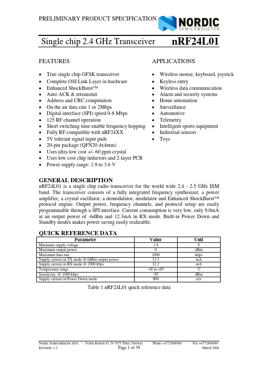
nRF24L01Single chip 2.4 GHz TransceiverFEATURES APPLICATIONS•True single chip GFSK transceiver •Wireless mouse, keyboard, joystick •Complete OSI Link Layer in hardware •Keyless entry•Enhanced ShockBurst™ •Wireless data communication•Auto ACK & retransmit •Alarm and security systems•Address and CRC computation •Home automation•On the air data rate 1 or 2Mbps •Surveillance•Digital interface (SPI) speed 0-8 Mbps •Automotive•125 RF channel operation •Telemetry•Short switching time enable frequency hopping •Intelligent sports equipment•Fully RF compatible with nRF24XX •Industrial sensors•5V tolerant signal input pads •Toys•20-pin package (QFN20 4x4mm)•Uses ultra low cost +/- 60 ppm crystal•Uses low cost chip inductors and 2-layer PCB•Power supply range: 1.9 to 3.6 VGENERAL DESCRIPTIONnRF24L01 is a single chip radio transceiver for the world wide 2.4 - 2.5 GHz ISMband. The transceiver consists of a fully integrated frequency synthesizer, a poweramplifier, a crystal oscillator, a demodulator, modulator and Enhanced ShockBurst™protocol engine. Output power, frequency channels, and protocol setup are easily programmable through a SPI interface. Current consumption is very low, only 9.0mAat an output power of -6dBm and 12.3mA in RX mode. Built-in Power Down andStandby modes makes power saving easily realizable.QUICK REFERENCE DATAUnit Parameter ValueMinimum supply voltage 1.9 VMaximum output power 0 dBmMaximum data rate 2000 kbpsSupply current in TX mode @ 0dBm output power 11.3 mASupply current in RX mode @ 2000 kbps 12.3 mATemperature range -40 to +85 °CSensitivity @ 1000 kbps -85 dBmSupply current in Power Down mode 900 nATable 1 nRF24L01 quick reference dataType NumberDescriptionVersionnRF24L01 20 pin QFN 4x4, RoHS & SS-00259 compliantD nRF24L01 IC Bare DiceD nRF24L01-EVKITEvaluation kit (2 test PCB, 2 configuration PCB, SW)1.0Table 2 nRF24L01 ordering informationBLOCK DIAGRAMDDD=0VD=0V=0VFigure 1 nRF24L01 with external components.PIN FUNCTIONSPin NamePin function Description1 CEDigital InputChip Enable Activates RX or TX mode2 CSN Digital InputSPI Chip Select 3SCK Digital InputSPI Clock4 MOSIDigital InputSPI Slave Data Input5 MISO Digital Output SPI Slave Data Output, with tri-state option6 IRQ Digital Output Maskable interrupt pin7 VDDPowerPower Supply (+3V DC) 8 VSS Power Ground (0V) 9 XC2 Analog Output Crystal Pin 2 10 XC1 Analog Input Crystal Pin 111 VDD_PA Power Output Power Supply (+1.8V) to Power Amplifier 12 ANT1 RF Antenna interface 1 13 ANT2 RFAntenna interface 2 14 VSS Power Ground (0V)15 VDD PowerPower Supply (+3V DC) 16 IREF Analog Input Reference current 17 VSS Power Ground (0V)18 VDD PowerPower Supply (+3V DC)19 DVDD Power Output Positive Digital Supply output for de-coupling purposes 20 VSSPowerGround (0V)Table 3 nRF24L01 pin functionPIN ASSIGNMENTVDDVSSANT2VSSCEVDD_PAANT1CSNMISO MOSI VDDIREFVSSIRQDVDDVSSXC2XC1VDDSCKFigure 2 nRF24L01 pin assignment (top view) for a QFN20 4x4 package.ELECTRICAL SPECIFICATIONSConditions: VDD = +3V, VSS = 0V, T A = - 40ºC to + 85ºCymbol Parameter (condition)NotesMin.Typ.Max. UnitsOperating conditionsVDD Supply voltage1.9 3.0 3.6 V TEMP Operating Temperature-40+27+85ºCDigital input pinV IH HIGH level input voltage 10.7VDD 5.25 VV IL LOW level input voltageVSS 0.3VDD VDigital output pinV OH HIGH level output voltage (I OH =-0.25m A ) VDD- 0.3 VDD VV OL LOW level output voltage (I OL =0.25m A) VSS 0.3 VGeneral RF conditionsf OP Operating frequency22400 2525 MHzf XTAL Crystal frequency16 MHz ∆f 1MFrequency deviation @ 1000kbps ±160 kHz ∆f 2MFrequency deviation @ 2000kbps ±320 kHz R GFSK Data rate ShockBurst™>0 2000 kbps F CHANNEL Channel spacing @ 1000kbps1 MHz F CHANNEL Channel spacing @ 2000kbps2 MHzTransmitter operationP RF Maximum Output Power30 +4 dBmP RFC RF Power Control Range 16 18 20 dB P RFCR RF Power A ccuracy ±4 dB P BW 20dB Bandwidth for Modulated Carrier(2000kbps)1800 2000 kHzP RF1 1st Adjacent Channel Transmit Power 2MHz -20 dBm P RF2 2nd Adjacent Channel Transmit Power 4MHz -50 dBm I VDD Supply current @ 0dBm output power 4 11.3 m AI VDD Supply current @ -18dBm output power 7.0m A I VDD Average Supply current @ -6dBm outputpower, Enhanced ShockBurst™50.05 m AI VDD Supply current in Standby-I mode 632 µA I VDD Supply current in power down900 nA1All digital inputs handle up to 5.25V signal inputs. Keep in mind that the VDD of the nRF24L01 must match theV IH of the driving device for output pins.2 Usable band is determined by local regulations 3Antenna load impedance = 15Ω+j88Ω 4Antenna load impedance = 15Ω+j88Ω. Effective data rate 1000kbps or 2000 kbps 5Antenna load impedance = 15Ω+j88Ω. Effective data rate 10kbps and full packets6Given for a 12pF crystal. Current when using external clock is dependent on signal swing.Receiver operationI VDD Supply current one channel 2000kbps 12.3 mAI VDD Supply current one channel 1000kbps 11.8 mARX SENS Sensitivity at 0.1%BER (@2000kbps) -82 dBm RX SENS Sensitivity at 0.1%BER (@1000kbps) -85 dBm C/I CO C/I Co-channel (@2000kbps) 778/119dB C/I1ST1st Adjacent Channel Selectivity C/I 2MHz 1/4 dB C/I2ND2nd Adjacent Channel Selectivity C/I 4MHz -21/-20 dB C/I3RD3rd Adjacent Channel Selectivity C/I 6MHz -27/-27 dB C/I CO C/I Co-channel (@1000kbps) 10911/1212dB C/I1ST1st Adjacent Channel Selectivity C/I 1MHz 8/8 dB C/I2ND2nd Adjacent Channel Selectivity C/I 2MHz -22/-21 dB C/I3RD3rd Adjacent Channel Selectivity C/I 3MHz -30/-30 dBTable 4 nRF24L01 RF specifications7Data rate is 2000kbps for the following C/I measurements8 According to ETSI EN 300 440-1 V1.3.1 (2001-09) page 279 nRF24L01 equal modulation on interfering signal10Data rate is 1000kbps for the following C/I measurements11 According to ETSI EN 300 440-1 V1.3.1 (2001-09) page 2712 nRF24L01 equal modulation on interfering signalPACKAGE OUTLINEnRF24L01 uses the QFN20 4x4 package, with matt tin plating.Package Type A A1 A3 K D/E e D2/E2 L L1 bSaw QFN20 (4x4 mm) MinTyp.Max0.800.850.950.000.020.050.20REF.0.20min4.0 BSC130.5 BSC2.502.602.700.350.400.450.15max0.180.250.30Figure 3 nRF24L01 Package Outline.13 BSC: Basic Spacing between Centers, ref. JEDEC standard 95, page 4.17-11/APackage marking:Abbreviations: B – Build Code, i.e. unique code for production sites, package type and test platform X – "X" grade, i.e. Engineering Samples (optional) YY – 2 digit Year number WW – 2 digit Week numberLL – 2 letter wafer lot number codeAbsolute Maximum RatingsSupply voltagesVDD............................- 0.3V to + 3.6V VSS..................................................0V Input voltageV I ..................................- 0.3V to 5.25V Output voltageV O .....................................VSS to VDDTotal Power DissipationP D (T A =85°C).............................60mWTemperaturesOperating Temperature…. - 40°C to + 85°C Storage Temperature….… - 40°C to + 125°CNote: Stress exceeding one or more of the limiting values may cause permanent damage to the device.ATTENTION!Electrostatic Sensitive Device Observe Precaution for handling.Glossary of Termsn R FB X2 4 L0 1 Y Y W W L LTerm DescriptionA CKAcknowledgementARTAutoRe-TransmitCE ChipEnableCLK ClockCRC Cyclic Redundancy CheckCSN ChipSelectNOTESB EnhancedShockBurst™ GFSK Gaussian Frequency Shift KeyingIRQ InterruptRequestISM Industrial-Scientific-Medical LNA LowNoiseAmplifierLSB Least Significant BitLSByte Least Significant ByteMbps Megabit per secondMCU Micro Controller UnitMISO Master In Slave OutMOSI Master Out Slave InMSB Most Significant BitMSByte Most Significant BytePCB Printed Circuit BoardPER Packet Error RatePID Packet Identity BitsPLD PayloadPRX PrimaryRXPTX PrimaryTXPWR_DWN PowerDownPWR_UP PowerUpRoHS Restriction of use of Certain Hazardous Substances RX ReceiveRX_DR Receive Data ReadySPI SerialPeripheralInterfaceTX TransmitTX_DS Transmit Data SentTable 5 GlossaryFUNCTIONAL DESCRIPTIONModes of operationThe nRF24L01 can be set in the following main modes depending on the level of the following primary I/Os and configuration registers:Mode PWR_UPregisterPRIM_RXregisterCE FIFOstateRX mode 1 1 1 -TX mode 1 0 1 Data in TX FIFOTX mode 1 0 1Î0 Stays in TX mode until packettransmission is finishedStandby-II 1 0 1 TX FIFO emptyStandby-I 1 - 0 No ongoing packet transmissionPower Down 0 - - -Table 6 nRF24L01 main modesAn overview of the nRF24L01 I/O pins in different modes is given in Table 7.Pin functions in the different modes of nRF24L01Pin Name Direction TX Mode RX Mode Standby Modes Power Down CE Input High Pulse >10µs High Low - CSN Input SPI Chip Select, active lowSCK Input SPIClock MOSI Input SPI Serial InputMISO Tri-stateOutputSPI Serial OutputIRQ Output Interrupt, active lowTable 7 Pin functions of the nRF24L01Standby ModesStandby-I mode is used to minimize average current consumption while maintaining short start up times. In this mode, part of the crystal oscillator is active. In Standby-II mode some extra clock buffers are active compared to Standby-I mode. Standby-II occurs when CE is held high on a PTX device with empty TX FIFO. The configuration word content is maintained during Standby modes. SPI interface may be activated. For start up time see Table 13.Power Down ModeIn power down nRF24L01 is disabled with minimal current consumption. When entering this mode the device is not active, but all registers values available from theSPI interface are maintained during power down and the SPI interface may be activated (CSN=0). For start up time see Table 13. The power down is controlled bythe PWR_UP bit in the CONFIG register.PRELIMINARY PRODUCT SPECIFICATIONnRF24L01 Single Chip 2.4 GHz Radio TransceiverPacket Handling MethodsnRF24L01 has the following Packet Handling Methods: • ShockBurst™ (compatible with nRF2401, nRF24E1, nRF2402 and nRF24E2 with 1Mbps data rate, see page 26) • Enhanced ShockBurst™ShockBurst™ShockBurst™ makes it possible to use the high data rate offered by nRF24L01 without the need of a costly, high-speed microcontroller (MCU) for data processing/clock recovery. By placing all high speed signal processing related to RF protocol on-chip, nRF24L01 offers the application microcontroller a simple SPI compatible interface, the data rate is decided by the interface-speed the micro controller itself sets up. By allowing the digital part of the application to run at low speed, while maximizing the data rate on the RF link, ShockBurst™ reduces the average current consumption in applications. In ShockBurst™ RX, IRQ notifies the MCU when a valid address and payload is received respectively. The MCU can then clock out the received payload from an nRF24L01 RX FIFO. In ShockBurst™ TX, nRF24L01 automatically generates preamble and CRC, see Table 12. IRQ notifies the MCU that the transmission is completed. All together, this means reduced memory demand in the MCU resulting in a low cost MCU, as well as reduced software development time. nRF24L01 has a three level deep RX FIFO (shared between 6 pipes) and a three level deep TX FIFO. The MCU can access the FIFOs at any time, in power down mode, in standby modes, and during RF packet transmission. This allows the slowest possible SPI interface compared to the average data-rate, and may enable usage of an MCU without hardware SPI.Enhanced ShockBurst™Enhanced ShockBurst™ is a packet handling method with functionality that makes bidirectional link protocol implementation easier and more efficient. In a typical bidirectional link, one will let the terminating part acknowledge received packets from the originating part in order to make it possible to detect data loss. Data loss can then be recovered by retransmission. The idea with Enhanced ShockBurst™ is to let nRF24L01 handle both acknowledgement of received packets and retransmissions of lost packets, without involvement from the microcontroller.Nordic Semiconductor ASA Revision: 1.2- Vestre Rosten 81, N-7075 Tiller, Norway-Phone +4772898900-Page 11 of 39Fax +4772898989 March 2006PRELIMINARY PRODUCT SPECIFICATIONnRF24L01 Single Chip 2.4 GHz Radio TransceiverTX3 TX2ipe 4P DataTX4 TX5Data PData PDa taTX1ipe 1PipeFigure 4: nRF24L01 in a star network configuration An nRF24L01 configured as primary RX (PRX) will be able to receive data trough 6 different data pipes, see Figure 4. A data pipe will have a unique address but share the same frequency channel. This means that up to 6 different nRF24L01 configured as primary TX (PTX) can communicate with one nRF24L01 configured as PRX, and the nRF24L01 configured as PRX will be able to distinguish between them. Data pipe 0 has a unique 40 bit configurable address. Each of data pipe 1-5 has an 8 bit unique address and shares the 32 most significant address bits. All data pipes can perform full Enhanced ShockBurst™ functionality. nRF24L01 will use the data pipe address when acknowledging a received packet. This means that nRF24L01 will transmit ACK with the same address as it receives payload at. In the PTX device data pipe 0 is used to received the acknowledgement, and therefore the receive address for data pipe 0 has to be equal to the transmit address to be able to receive the acknowledgement. See Figure 5 for addressing example.t Da a pe Pi 25Frequency Channel Nipe 3TX6Da 0 ipe ta PRXNordic Semiconductor ASA Revision: 1.2- Vestre Rosten 81, N-7075 Tiller, Norway-Phone +4772898900-Page 12 of 39Fax +4772898989 March 2006PRELIMINARY PRODUCT SPECIFICATIONnRF24L01 Single Chip 2.4 GHz Radio TransceiverFigure 5: Example on how the acknowledgement addressing is done An nRF24L01 configured as PTX with Enhanced ShockBurst™ enabled, will use the ShockBurst™ feature to send a packet whenever the microcontroller wants to. After the packet has been transmitted, nRF24L01 will switch on its receiver and expect an acknowledgement to arrive from the terminating part. If this acknowledgement fails to arrive, nRF24L01 will retransmit the same packet until it receives an acknowledgement or the number of retries exceeds the number of allowed retries given in the SETUP_RETR_ARC register. If the number of retries exceeds the number of allowed retries, this will be showed by the STATUS register bit MAX_RT which gives an interrupt. Whenever an acknowledgement is received by an nRF24L01 it will consider the last transmitted packet as delivered. It will then be cleared from the TX FIFO, and the TX_DS IRQ source will be set high. With Enhanced ShockBurst™ nRF24L01 offers the following benefits: • Highly reduced current consumption due to short time on air and sharp timing when operating with acknowledgement traffic • Lower system cost. Since the nRF24L01 handles all the high-speed link layer operations, like re-transmission of lost packet and generating acknowledgement to received packets, it is no need for hardware SPI on the system microcontroller to interface the nRF24L01. The interface can be done by using general purpose IO pins on a low cost microcontroller where the SPI is emulated in firmware. With the nRF24L01 this will be sufficient speed even when running a bi-directional link. • Greatly reduced risk of “on-air” collisions due to short time on air • Easier firmware development since the link layer is integrated on chipNordic Semiconductor ASA Revision: 1.2 - Vestre Rosten 81, N-7075 Tiller, Norway Phone +4772898900 -Page 13 of 39Fax +4772898989 March 2006PRELIMINARY PRODUCT SPECIFICATIONnRF24L01 Single Chip 2.4 GHz Radio TransceiverEnhanced ShockBurst™ Transmitting Payload:1. The configuration bit PRIM_RX has to be low. 2. When the application MCU has data to send, the address for receiving node (TX_ADDR) and payload data (TX_PLD) has to be clocked into nRF24L01 via the SPI interface. The width of TX-payload is counted from number of bytes written into the TX FIFO from the MCU. TX_PLD must be written continuously while holding CSN low. TX_ADDR does not have to be rewritten if it is unchanged from last transmit. If the PTX device shall receive acknowledge, data pipe 0 has to be configured to receive the acknowledgement. The receive address for data pipe 0 (RX_ADDR_P0) has to be equal to the transmit address (TX_ADDR) in the PTX device. For the example in Figure 5 the following address settings have to be performed for the TX5 device and the RX device: TX5 device: TX_ADDR = 0xB3B4B5B605 TX5 device: RX_ADDR_P0 = 0xB3B4B5B605 RX device: RX_ADDR_P5 = 0xB3B4B5B605 3. A high pulse on CE starts the transmission. The minimum pulse width on CE is 10 µs. 4. nRF24L01 ShockBurst™: • Radio is powered up • 16 MHz internal clock is started. • RF packet is completed (see the packet description) • Data is transmitted at high speed (1 Mbps or 2 Mbps configured by MCU). 5. If auto acknowledgement is activated (ENAA_P0=1) the radio goes into RX mode immediately. If a valid packet has been received in the valid acknowledgement time window, the transmission is considered a success. The TX_DS bit in the status register is set high and the payload is removed from TX FIFO. If a valid acknowledgement is not received in the specified time window, the payload is resent (if auto retransmit is enabled). If the auto retransmit counter (ARC_CNT) exceeds the programmed maximum limit (ARC), the MAX_RT bit in the status register is set high. The payload in TX FIFO is NOT removed. The IRQ pin will be active when MAX_RT or TX_DS is high. To turn off the IRQ pin, the interrupt source must be reset by writing to the status register (see Interrupt chapter). If no acknowledgement is received for a packet after the maximum number of retries, no further packets can be sent before the MAX_RX interrupt is cleared. The packet loss counter (PLOS_CNT) is incremented at each MAX_RT interrupt. I.e. ARC_CNT counts the number of retries that was required to get a single packet through. PLOS_CNT counts the number of packets that did not get through after maximum number of retries. 6. The device goes into Standby-I mode if CE is low. Otherwise next payload in TX FIFO will be sent. If TX FIFO is empty and CE is still high, the device will enter Standby-II mode. 7. If the device is in Standby-II mode, it will go to Standby-I mode immediately if CE is set low.Enhanced ShockBurstTM Receive Payload:1. RX is selected by setting the PRIM_RX bit in the configuration register to high. All data pipes that shall receive data must be enabled (EN_RXADDR register),Nordic Semiconductor ASA Revision: 1.2 - Vestre Rosten 81, N-7075 Tiller, Norway Phone +4772898900 Fax +4772898989 March 2006Page 14 of 39PRELIMINARY PRODUCT SPECIFICATIONnRF24L01 Single Chip 2.4 GHz Radio Transceiver2. 3. 4.5. 6. 7. 8.auto acknowledgement for all pipes running Enhanced ShockBurst™ has to be enabled (EN_AA register), and the correct payload widths must be set (RX_PW_Px registers). Addresses have to be set up as described in item 2 in the Enhanced ShockBurst™ transmit payload chapter above. Active RX mode is started by setting CE high. After 130µs nRF24L01 is monitoring the air for incoming communication. When a valid packet has been received (matching address and correct CRC), the payload is stored in the RX-FIFO, and the RX_DR bit in status register is set high. The IRQ pin will be active when RX_DR is high. RX_P_NO in status register will indicate what data pipe the payload has been received in. If auto acknowledgement is enabled, an acknowledgement is sent back. MCU sets the CE pin low to enter Standby-I mode (low current mode). MCU can clock out the payload data at a suitable rate via the SPI interface. The device is now ready for entering TX or RX mode or power down mode.Two way communication with payload in both directionsIf payload shall be sent in both directions, the PRIM_RX register must be toggled by redefining the device from PRX to PTX or vice versa. The controlling processors must handle the synchronicity between a PTX and a PRX. Data buffering in both RX FIFO and TX FIFO simultaneously is possible, but restricted to data pipes 1 to 5. The third level in TX FIFO shall only be written in RX, TX or Standby-II mode if data is stored in RX FIFOAuto Acknowledgement (RX)The auto acknowledgement function reduces the load of the external microcontroller, and may remove the need for dedicated SPI hardware in a mouse/keyboard or comparable systems, and hence reduce cost and average current consumption. Auto acknowledgement can be configured individually for each data pipe via the SPI interface. If auto acknowledgement is enabled and a valid packet (correct data pipe address and CRC) is received, the device will enter TX mode and send an acknowledgement packet. After the device has sent the acknowledgement packet, normal operation resumes, and the mode is determined by the PRIM_RX register and CE pin.Auto Re-Transmission (ART) (TX)An auto retransmission function is available. It will be used at the TX side in an auto acknowledgement system. In the SETUP_RETR register it will be possible to state how many times the data in the data register will be resent if data is not acknowledged. After each sending, the device will enter RX mode and wait a specified time period for acknowledgement. When the acknowledgement packet is received, the device will return to normal transmit function. If there is no more unsent data in the TX FIFO and the CE pin is low, the device will go into Standby-I mode. If the acknowledgement is not received, the device will go back to TX mode and resend the data. This will continue until acknowledgment is received, or a time out occursNordic Semiconductor ASA Revision: 1.2 - Vestre Rosten 81, N-7075 Tiller, Norway Phone +4772898900 Fax +4772898989 March 2006Page 15 of 39PRELIMINARY PRODUCT SPECIFICATIONnRF24L01 Single Chip 2.4 GHz Radio Transceiver(i.e. the maximum number of sending is reached). The only way to reset this is to set the PWR_UP bit low or let the auto retransmission finish. A packet loss counter will be incremented each time a packet does not succeed to reach the destination before time out. (Time out is indicated by the MAX_RT interrupt.) The packet loss counter is reset when writing to the RF channel register.Packet Identity (PID) and CRC used by Enhanced ShockBurstTMEach packet contains a two bit wide PID field to detect if the received packet is new or resent. The PID will prevent that the PRX device presents the same payload more than once to the microcontroller. This PID field is incremented at the TX side for each new packet received via the SPI interface. The PID and CRC field is used by the PRX device to determine whether a packet is resent or new. When several data is lost on the link, the PID fields may in some cases become equal to last received PID. If a packet has the same PID as the previous packet, nRF24L01 will compare the CRC sums from both packets. If they also are equal, the last received packet is considered as a copy of the previous and is discarded. 1: PRX device: The PRX device compares the received PID with the last PID. If the PID fields are different, the packet is considered to be new. If the PID is equal to last received PID, the received packet might be the same as last time. The receiver must check if the CRC is equal to the previous CRC. If the CRC is equal to the previous one, the packet is probably the same, and will be discarded. 2: PTX device: The transmitter increments the PID field each time it sends a new packet.TX side functionalityStartRX side functionalityStartNew packet from MCU?YesPID equal last PID?YesCRC equal last CRC?increment PID No No New packet is valid for MCUYes NoDiscard packet as a copyEndEndFigure 6 PID generation/detectionNordic Semiconductor ASA Revision: 1.2 - Vestre Rosten 81, N-7075 Tiller, Norway Phone +4772898900 Fax +4772898989 March 2006Page 16 of 39PRELIMINARY PRODUCT SPECIFICATIONnRF24L01 Single Chip 2.4 GHz Radio TransceiverThe length of the CRC is configurable through the SPI interface. It is important to notice that the CRC is calculated over the whole packet including address, PID and payload. No packet is accepted as correct if the CRC fails. This is an extra requirement for packet acceptance that is not illustrated in the figure above.Stationary Disturbance Detection – CDCarrier Detect (CD) is set high when an in-band RF signal is detected in RX mode, otherwise CD is low. The internal CD signal is filtered before presented to CD register. The internal CD signal must be high for at least 128µs. In Enhanced ShockBurst™ it is recommended to use the Carrier Detect functionality only when the PTX device does not succeed to get packets through, as indicated by the MAX_RT interrupt for single packets and by the packet loss counter (PLOS_CNT) if several packets are lost. If the PLOS_CNT in the PTX device indicates to high rate of packet losses, the device can be configured to a PRX device for a short time (Tstbt2a + CD-filter delay = 130µs+128µs = 258µs) to check CD. If CD was high (jam situation), the frequency channel should be changed. If CD was low (out of range), it may continue on the same frequency channel, but perform other adjustments. (A dummy write to the RF_CH will clear the PLOS_CNT.)Data PipesnRF24L01 configured as PRX can receive data addressed to 6 different data pipes in one physical frequency channel. Each data pipe has its own unique address and can be configured to have individual behavior. The data pipes are enabled with the bits in the EN_RXADDR register. By default only data pipe 0 and 1 are enabled. The address for each data pipe is configured in the RX_ADDR_Px registers. Always ensure that none of the data pipes have the exact same address. Data pipe 0 has a unique 40 bit configurable address. Data pipes 1-5 share the 32 most significant address bits and have only the LSByte unique for each data pipe. Figure 7 shows an example of how data pipes 0-5 are addressed. All pipes can have up to 40 bit address, but for pipe 1-5 only the LSByte is different, and the LSByte must be unique for all pipes.Nordic Semiconductor ASA Revision: 1.2- Vestre Rosten 81, N-7075 Tiller, Norway-Phone +4772898900-Page 17 of 39Fax +4772898989 March 2006PRELIMINARY PRODUCT SPECIFICATIONnRF24L01 Single Chip 2.4 GHz Radio TransceiverByte 4 Data pipe 0 (RX_ADDR_P0) Data pipe 1 (RX_ADDR_P1) Data pipe 2 (RX_ADDR_P2) Data pipe 3 (RX_ADDR_P3) Data pipe 4 (RX_ADDR_P4) Data pipe 5 (RX_ADDR_P5) 0xE7 0xC2 0xC2 0xC2 0xC2 0xC2 Byte 3 0xD3 0xC2 0xC2 0xC2 0xC2 0xC2 Byte 2 0xF0 0xC2 0xC2 0xC2 0xC2 0xC2 Byte 1 0x35 0xC2 0xC2 0xC2 0xC2 0xC2 Byte 0 0x77 0xC2 0xC3 0xC4 0xC5 0xC6Figure 7: Addressing data pipes 0-5 When a packet has been received at one of the data pipes and the data pipe is setup to generate acknowledgement, nRF24L01 will generate an acknowledgement with an address that equals the data pipe address where the packet was received. Some configuration settings are common to all data pipes and some are individual. The following settings are common to all data pipes: • CRC enabled/disabled (CRC always enabled when ESB is enabled) • CRC encoding scheme • RX address width • Frequency channel • RF data rate • LNA gain • RF output powerNordic Semiconductor ASA Revision: 1.2- Vestre Rosten 81, N-7075 Tiller, Norway-Phone +4772898900-Page 18 of 39Fax +4772898989 March 2006。
含表皮生长因子受体(EGFR)启动子萤光素酶报告基因的三阴性乳腺癌细胞模型的建立
918细胞与分子免疫学杂志(Chin J Cell M ol ImmU n〇l)2020, 36(10) .论著•文章编号:1007 -8738(2020)10 -0918 -06含表皮生长因子受体(E G FR)启动子萤光素酶报告基因的三阴性乳腺癌 细胞模型的建立梁丹丹、王春苗\李俊莹、覃良淑\粟正英2,侯华新|+G广西医科大学药物分析教研室,广西南宁530021; 2广西国际壮医医院药学部,广西南宁530201)[摘要]目的建立稳定表达人表皮生长因子受体(EGFR)启动子及萤光素酶(Luc)报告基因的三阴性乳腺癌细胞系,并对其 应用进行初步验证。
方法采用基因重组技术,构建含有EGFR启动子以及Luc报告基因的慢病毒载体,并感染MDA-M B231 细胞,经过嘌呤霉素筛选获得能稳定表达Luc活性的MDA-M B231-EGFR-Luc2细胞系;分别采用EGFR激活剂EG F以及抑制剂 吉非替尼处理细胞后检测Luc活性变化。
结果通过基因测序和质粒双酶切鉴定,EGFR基因启动子Luc报告基因-慢病毒表 达载体构建成功,经过嘌呤霉素筛选获得稳定表达Luc的MDA-MB231-EGFR-LU C2细胞;EGF可剂量依赖性的增加细胞中Luc 的活性,而吉非替尼则相反。
结论建立了MDA-M B231-EGFR-Luc2稳定表达EGFR启动子及Luc报告基因细胞系,为高通量 筛选靶向EGFR的抗肿瘤药物提供一类新的细胞模型。
[关键词]表皮生长因子受体;启动子;萤光素酶报告基因;三阴性乳腺癌;MDA-MB231细胞[中图分类号]Q279, R737.9, R392-33, R965 [文献标志码]A表皮生长因子受体(epidermal growth factor receptor,E G F R)为跨膜酪氨酸激酶蛋白,是酪氨酸 激酶受体超家族的成员之一。
E G F R调控的信号通 路在细胞增殖、存活、分化、迁移中发挥着关键作 用[1_3],E G F R在肺癌、卵巢癌、鼻咽癌、乳腺癌等 多种恶性肿瘤中均呈高表达且与患者的预后不良密 切相关[4_6]。
HMGB1MMP-9及VEGF-C在老年肺癌患者组织中水平变化及意义研究
HMGB1MMP-9及VEGF-C在老年肺癌患者组织中水平变化及意义研究【摘要】本研究旨在探讨HMGB1、MMP-9及VEGF-C在老年肺癌患者组织中的水平变化及意义。
研究发现HMGB1、MMP-9和VEGF-C在老年肺癌组织中的表达水平均显著升高,且三者之间存在相关性。
进一步的分析表明,这些蛋白的水平变化可能与老年肺癌的发生和发展密切相关。
HMGB1MMP-9及VEGF-C在老年肺癌中可能扮演着重要作用,并成为潜在的治疗靶点。
未来的研究应该进一步阐明这些蛋白在老年肺癌中的作用机制,为临床治疗提供更多的依据。
本研究为老年肺癌的治疗和预防提供了有益的参考。
【关键词】关键词:老年肺癌、HMGB1、MMP-9、VEGF-C、组织水平、相关性、治疗靶点、作用机制。
1. 引言1.1 研究背景肺癌是老年人群中常见的恶性肿瘤之一,其发病率和死亡率均位居各种癌症之首。
随着人口老龄化趋势的加剧,老年肺癌的发病率也在不断增加。
对老年肺癌的病理生物学机制进行深入研究,对于早期诊断和治疗具有极其重要的意义。
高迁移率族蛋白1(HMGB1)、基质金属蛋白酶-9(MMP-9)和血管内皮生长因子C(VEGF-C)作为肿瘤相关蛋白,在肿瘤的发生发展过程中发挥着重要作用。
近年来的研究表明,这三种蛋白在肺癌中的表达水平与肿瘤的浸润、转移和预后密切相关。
在老年肺癌患者中,关于HMGB1、MMP-9和VEGF-C的表达变化及其临床意义的研究还相对较少。
本研究旨在探讨HMGB1、MMP-9和VEGF-C在老年肺癌患者组织中的表达水平及其相关性,进一步揭示这些蛋白在老年肺癌发生发展中的作用机制。
通过深入研究这些生物标志物的变化,有望为老年肺癌的早期诊断、治疗和预后评估提供新的指导和策略。
1.2 研究目的本研究的主要目的是探讨HMGB1、MMP-9和VEGF-C在老年肺癌患者组织中的表达水平及其相关性,以及对老年肺癌的病理生理学机制进行初步探讨。
1SMA5913BT3中文资料(motorola)中文数据手册「EasyDatasheet-矽搜」
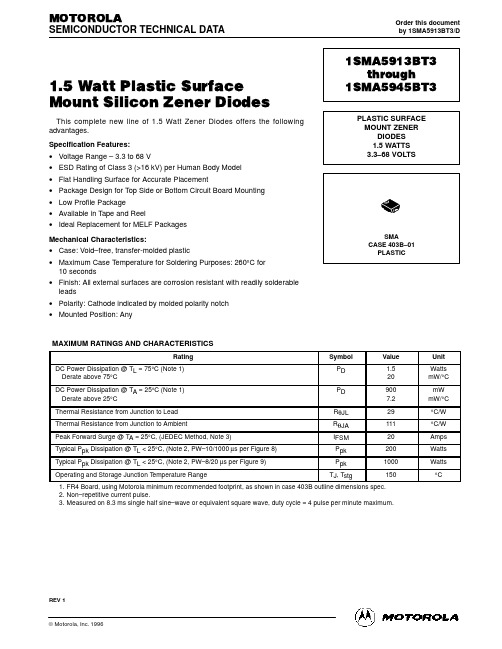
1SMA5913BT3中文资料(motorola)中文数据手册「EasyDatasheet-矽搜」摩托罗拉半导体技术资料订购此文件通过1SMA5913BT3 / D1SMA5913BT3通过1.5瓦塑料表面安装硅齐纳二极管1.5瓦齐纳二极管这个完整新行提供以下优点.规格特点:电压范围 - 3.3至68五ESD额定值3级(16千伏)每人体模型平操作面精确定位包装设计顶部侧面或底部电路电路板安装薄型封装可在磁带和卷轴理想替代MELF软件包机械特性:案例:无空洞,转移模塑塑料最大外壳焊接温度目:260℃,10秒表面处理:所有外部表面耐腐蚀用随手可焊leads极性:负极通过模压极性缺口指示安装位置:任何1SMA5945BT3塑料表面MOUNT ZENER二极管1.5瓦3.3-68伏SMACASE 403B–01塑料最大额定值和特性等级DC功率耗散@ TL = 75°C(注1)减免上述75℃DC功耗@ TA = 25°C(注1)减免上述25℃热阻结到铅从结到环境热阻峰值正向浪涌@ TA = 25°C,(JEDEC方法,注3)典型Ppk耗散@ TL 25°C,(注2,PW-10/1000μs每图8)典型Ppk耗散@ TL 25°C,(注2,PW-8/20μs按照图9)工作和存储结温范围符号PDPDR JLR JAIFSMPpkPpkTJ, Tstg值1.5209007.229111202001000150单元WattsmW/°CmWmW/°C°C/W°C/WA mpsWattsWatts°C1. FR4电路板,采用摩托罗拉最低推荐足迹,如图情况403B外形尺寸规格.2.不重复电流脉冲.3.在测量8.3ms单一正弦半波或等效方波,占空比=每分钟最多4个脉冲.REV 1Motorola, Inc. 19961SMA5913BT3通过1SMA5945BT31电气特性(V F = 1.5伏特@ IF = 200 mA时所有类型)最大齐纳阻抗设备额定齐纳电压VZ @IZT伏特3.3 3.63.94.34.75.15.66.26.87.58.29.11011121315161820222427303336394347566268测试当前IZT毫安113.6 104.2 96.1 87.2 79.8 73.5 66.9 60.5 55.1 50 45.7 41.2 37.5 34.1 31.2 28.8 25 23.4 20.8 18.7 17 15.6 13.911.4 10.49.68.78.07.36.76.05.5ZZT @ IZT Ohms109.07.56.05.04.02.02.02.53.03.54.04.55.56.57.09.01014 17.5 19 23 26 33 38 45 53 67 70 86 100 120 ZZK Ohms 500 500 500 500 500 350 250 200 200 400 400 500 500550 550 600 600 650 650 650 700 700 750 800 850 900 950 1000 1100 1300 1500 1700 IZK mA 1.0 1.0 1.0 1.0 1.0 1.0 1.0 1.00.50.50.50.250.250.250.250.250.250.250.250.250.250.250.250.250.250.250.250.250.250.250.250.25最大反向漏电流IRμA5035.52.5 2.5 2.5 2.5 2.5 2.5 2.5 2.5 2.5 0.5 0.5 0.5 0.5 0.5 0.5 0.5 0.5 0.5 0.5 0.5 0.5 0.5 0.5 0.5 0.5 0.5 0.5 0.5 0.5VR Volts 1.0 1.0 1.0 1.01.52.03.04.05.26.56.87.08.08.49.1 9.911.412.213.715.216.7 18.2 20.6 22.8 25.1 27.4 29.735.8 38.8 42.6 47.1 51.7最大DC 齐纳电流IZM mAdc 455 417 385 349 319 294 268 242 221 200 183 165 150 136 125 115 100948375635650454238353229272422Devce标志1SM A5913BT3 1SM A5914BT3 1SM A5915BT3 1SM A5916BT3 1SM A5917BT3 1SM A5918BT3 1SM A5919BT3 1SM A5920BT3 1SM A5921BT3 1SM A5922BT3 1SM A5923BT3 1SM A5924BT3 1SM A5925BT3 1SM A5926BT3 1SM A5927BT3 1SM A5928BT3 1SM A5929BT3 1SM A5930BT3 1SM A5931BT3 1SM A5932BT3 1SM A5933BT3 1SM A5934BT3 1SM A5935BT3 1SM A5936BT3 1SM A5937BT3 1SM A5938BT3 1SM A5939BT3 1SM A5940BT3 1SM A5941BT3 1SM A5942BT3 1SM A5943BT3 1SM A5944BT3 1SM A5945BT3813B 814B 815B 816B 817B 818B 819B 820B 821B 822B 823B 824B 825B 826B 827B 828B 829B 830B 831B 832B 833B 834B 835B 836B 837B 838B 839B 840B 841B 842B 843B 844B 845B注:公差和电压指定公差代号 - 列出型号数字表示公差±5%.24100PD,最大功耗(瓦)1251503.2102.4TL1.610.80025TA0.15075100T,温度(℃)0246V Z,齐纳电压(伏)810图1.稳态功率降额图2:VZ - 3.3通10伏86420–2–42V Z @ IZTV Z,温度系数(毫伏/°C) V Z,温度系数(毫伏/°C)10100V Z @ IZT468V Z,齐纳电压(伏)10121010100图3.齐纳电压 - 3.3?12伏特图4.齐纳电压 - 14到68伏特ZZ,动态阻抗(欧姆)100IZ(dc) = 1 mA1010毫安IZ (有效值)= 0.1 IZ (直流)100V Z,齐纳电压(伏)20毫安10图5.影响齐纳电压1SMA5913BT3通过1SMA5945BT3 31000测量@零偏置测量@V Z/210非重复,指数脉冲波形,TJ = 25°C1100PPK,峰值功率(KW )100C,电容(pF )0.1TJ = 25°C10击穿电压(V )0.010.010.11TP,脉冲宽度(毫秒)10图6.电容曲线图7.典型脉冲额定值曲线120IPPM ,峰值脉冲电流(%)= 10μs100806040200TA = 25°CPW (ID ),被定义为点峰值电流峰值衰减到伊普50%. Ippm半值 - IPP / 210/1000μs 波形A S 定义R.E.A . td123T,时间(ms )45120IPPM ,峰值脉冲0.9 IPEA K电流(%)806040200.1 IPEA KT = 8μs00T 20μs0.020.040.06T,时间(ms )0.080.18/20μs 波形A S 定义A NSI C62.1和IEC 801-5.0.5 IPEA K图8.脉冲波形图9.脉冲波形4外形尺寸S A0.1574.00.07872.0D B0.07872.0inchesmmSMACNOT ES:1.DIM ENSIONING AND T OLERANCING PER ANSI Y14.5M, 1982.2.CONT ROLLING DIM ENSION: INCH.INCHESMIN MA X0.1600.1800.0900.1150.0750.1050.0500.0640.0040.0080.0060.0160.0300.0600.1900.220MILLIMETERSMIN MA X4.06 4.572.29 2.921.912.671.27 1.630.100.200.150.410.76 1.524.835.59K J H DIMABCDHJKSCA SE 403B–01 发行?5。
植物病害诊断试剂盒
植物病害诊断试剂盒美国阿格迪agdia 公司是全球最大的植物病害诊断试剂生产商,产品品种最多,可检测项目多达200多个。
包装规格最全,不同的包装规格适合不同规模的实验室。
从中您一定能发现适合您使用的产品。
选购试剂说明,请仔细阅读。
1,kit, 订货号PSAxxxxx/xxxx 或PSPxxxxx/xxxx 为完整的试剂盒包装,包括样品提取缓冲液、包被好抗体的微孔板(可拆分)、酶标记物、稀释液、缓冲液、底物发色剂、阳性质控(如果应该供应)。
特别注明Indirect ELISA 方法的kit 包括未包被的微孔板及联接用的抗体,所含有的其他组分同上。
2, Reagent Set, 订货号SRAxxxxx/xxxx ,XRAxxxxx/xxxx或SRPxxxxx/xxxx 只含有未包被的微孔板、包被需要的抗体或联接用的抗体、酶标记物。
其他试剂如样品提取缓冲液、稀释液、缓冲液、底物发色剂、质控物需另外订购或自己配制。
我公司销售原厂的上述试剂,详见目录。
3, Bacterial Reagent Set, 订货号BRAxxxxx/xxxx 只含有未包被的微孔板、包被需要的抗体或联接用的抗体、酶标记物。
其他试剂如样品提取缓冲液、稀释液、缓冲液、底物发色剂、质控物需另外订购或自己配制。
我公司销售原厂的上述试剂,详见目录。
4, Bacterial ID订货号BIDxxxxx/xxxx 为完整的试剂盒包装,包括样品提取缓冲液、包被好抗体的微孔板(可拆分)、酶标记物、稀释液、缓冲液、底物发色剂、质控(如果应该供应)。
用于鉴定培养基中或有病症植物提取液中的细菌。
操作简便快速。
5, PS A或SR A中的A代表碱性磷酸酶标记;PS P或SR P中的P代表过氧化物酶标记。
6, Immunostrip test, 为检试纸条,操作简单,几分钟内得到结果,非常适合于现场检测。
该试条必须与相应的样品提取缓冲液配套使用。
实验室需要单独购买该样品提取缓冲液,详见目录。
BDPharmingen
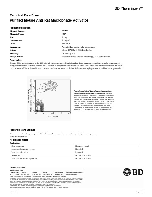
BD Pharmingen™Technical Data SheetPurified Mouse Anti-Rat Macrophage ActivatorProduct InformationMaterial Number:555020Alternate Name: RMASize: 0.5 mgConcentration:0.5 mg/mlClone: anti-RMAImmunogen:Activated Lewis rat alveolar macrophagesIsotype:Mouse (BALB/c X C57BL/6) IgG1, κQC Testing: RatReactivity:Aqueous buffered solution containing ≤0.09% sodium azide.Storage Buffer:DescriptionThe anti-RMA antibody reacts with a 120-kDa cell-surface antigen, which is found on tissue macrophages, resident alveolar macrophages,thioglycollate-elicited peritoneal exudate cells, a subset of peripheral blood monocytes, and a small subset of pulmonary interstitial dendriticcells. mAb anti-RMA activates DNA and protein synthesis and promotes fusion of alveolar macrophages to form multinucleated giant cells.Two-color analysis of Macrophage Activator antigenexpression on peripheral blood monocytes.Lewis ratperipheral blood leukocytes were incubated simultaneouslywith FITC-conjugated anti-rat CD11b mAb WT.5 (Cat. no.554982) and purified mAb anti-RMA. The purified antibodywas detected with biotinylated anti-mouse IgG1 mAb A85-1(Cat. no. 553441), followed by Streptavidin-PE (Cat. no.554061). Mononuclear cells were selected according totheir forward vs. side-scatter profile. Flow cytometry wasperformed on a BD FACScan™ flow cytometry system.Preparation and StorageThe monoclonal antibody was purified from tissue culture supernatant or ascites by affinity chromatography.Store undiluted at 4°C.Application NotesApplicationFlow cytometry Routinely TestedImmunohistochemistry-frozen ReportedImmunoprecipitation ReportedWestern blot Not RecommendedImmunohistochemistry-paraffin Not RecommendedSuggested Companion ProductsCatalog Number Size CloneName554982FITC Mouse Anti-Rat CD11b0.5 mg WT.5 553441Biotin Rat Anti-Mouse IgG10.5 mg A85-1 554061PE Streptavidin0.5 mg(none) 557273Purified Mouse IgG1, κ Isotype Control0.5 mg MOPC-31C Product Notices1.Since applications vary, each investigator should titrate the reagent to obtain optimal results.2.Please refer to /pharmingen/protocols for technical protocols.3.Sodium azide is a reversible inhibitor of oxidative metabolism; therefore, antibody preparations containing this preservative agent must not be used in cell cultures nor injected into animals. Sodium azide may be removed by washing stained cells or plate-bound antibody or dialyzing soluble antibody in sodium azide-free buffer. Since endotoxin may also affect the results of functional studies, we recommend the NA/LE (No Azide/Low Endotoxin) antibody format, if available, for in vitro and in vivo use.4.Caution: Sodium azide yields highly toxic hydrazoic acid under acidic conditions. Dilute azide compounds in running water before discarding to avoid accumulation of potentially explosive deposits in plumbing.ReferencesLazarus D, Yamin M, McCarthy K, Schneeberger EE, Kradin R. Anti-RMA, a murine monoclonal antibody, activates rat macrophages: II. Induction of DNA synthesis and formation of multinucleated giant cells.. Am J Respir Cell Mol Biol. 1990; 3(2):103-111.(Clone-specific: Activation)Xia WJ, Schneeberger EE, McCarthy K, Kradin RL. Accessory cells of the lung. II. Ia+ pulmonary dendritic cells display cell surface antigen heterogeneity. Am J Respir Cell Mol Biol. 1991; 5(3):276-283.(Biology)Yamin M, Lazarus D, Schneeberger EE, McCarthy K, Xia WJ, Kradin R. Anti-RMA: a murine monoclonal antibody that activates rat macrophages. I. Distribution and characterization of the RMA antigen. Cell Mol Biol (Noisy-le-grand). 1990; 2:207-215.(Immunogen: Activation, Immunohistochemistry, Immunoprecipitation, Western blot)。
1SMA5918中文资料
元器件交易网
Rating and Typical Characteristic Curves (TA = 25°C)
4 100
PD , MAXIMUM POWER DISSIPATION (WATTS)
IZ, ZENER CURRENT (mA) 125 150
3.2
10
100
Figure 3. Zener Voltage – 3.3 to 12 Volts
Figure 4. Zener Voltage – 14 to 68 Volts
ZZ, DYNAMIC IMPEDANCE (OHMS)
100 IZ(dc) = 1 mA
10
10 mA IZ(rms) = 0.1 IZ(dc) 100 VZ, ZENER VOLTAGE (VOLTS)
NOTE: Tolerance and Voltage Designation Tolerance designation – The type number listed indicates a tolerance of ±5%.
MOTOROLA 2
1SMA5913BT3 through 1SMA5945BT3
1000 MEASURED @ ZERO BIAS MEASURED @ VZ/2 10 NONREPETITIVE, EXPONENTIAL PULSE WAVEFORM, TJ = 25°C 1
100
Ppk , PEAK POWER (kW) 100
C, CAPACITANCE (pF)
0.1
TJ = 25°C 10 10 BREAKDOWN VOLTAGE (VOLTS) 0.01 0.01 0.1 1 TP, PULSE WIDTH (ms) 10
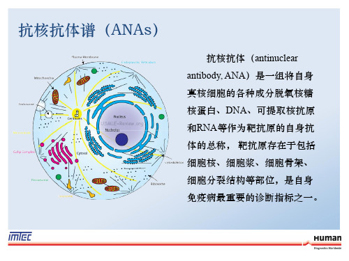
ANA检测
IMTEC ANA相关产品
ACR --ANA检测
100年前,保罗·艾尔利希首次提出“自身免疫”概念 60年前,ANA检测方法的诞生,临床免疫学的里程碑 ANA检测方法逐年更新,敏感性和特异性得以提高 2009年,将间接免疫荧光法(IIF)作为ANA检测的金标准 2014年,IIF法就已经被称为“参考方法” 2015年,Wener教授建议用特异性方法配合检测(ELISA 法或印迹法)
ANA实验室检测策略
多特异性实验 IFA(Hep-2)或ELISA筛查
阴性
阴性,临床症 状明显
阳性
推荐检测策略
单特异性靶抗原抗体 确认LIA或ELISA
报告结果
IMTEC ANA Elisa Screen
▪德国原装进口,品质保证 ▪全球首个ANA-ELISA定量检测试剂盒 ▪采用专利的细胞活化包板技术,包被 的是HeLa细胞核和纯化抗原混合物 ▪更高的特异性和敏感度 ▪校准品可溯源至美国CDC标准
自身免疫性疾病
“5D”疾病
自身免疫性疾病研究背景
1854-1915年, Paul Ehrlich 用(“horror auto-toxicus”) 描述 自身免疫性疾病
1940年, Waaler 描述了一种 因子(之后发现是类风湿因子)
1948年, Hargraves et al. 发现红斑狼疮细胞, 巨噬细胞吞噬 变性细胞
ANA检测已成为临床上的一个极重要的自身免疫病的筛查实验。
ANA检测的临床意义
相关疾病 系统性红斑狼疮 活动期 非活动期 药物诱导的红斑狼疮 混合性结缔组织病 类风湿性关节炎 进行性系统性硬化症 多发性肌炎及皮肌炎 干燥综合征 慢性活动性肝炎 溃疡性结肠炎 其它风湿病 正常人
SMAD4在血管瘤中的表达及意义

和阳性面积率 ( s 矗 )
1 Jn i stsi siaaTsy si o eEl n innMaao h.Ihh r u oh,B y ie ,oL E Bon e S N ir
R.R cn r g e si t de f n a t eh ma go .Th o r e e t o r s su iso f n i e n ima p n i l eJ u —
1 材 料 和 方 法 1 1 材 料 .
具体步骤 : 4 m 组织切片常规脱蜡 入水 ; 抗原修复 ( ① , u ② 柠檬 酸缓冲液微波抗原 修 复法 )③ 滴 加 3 过 氧化 氢 ,7 ; 3  ̄ 盒 C湿 孵育 1 mi 0 n以抑 制 内源性 过 氧化 物 酶活 性 ; 正 常 羊 血 清 ④ 3 ℃湿盒孵育 1 ri 7 0 n以减少非特异性背景 ; 分别滴加一抗 ; a ⑤ ⑥ 滴加链霉 素抗生物素蛋 白一 过氧化物复合物 3 ℃湿盒孵育 ; 7
片 随 机 选 取 5个 完 整 而 不 重 叠 的 高倍 镜 视 野 ( 0 ), 定 每 ×4 0 测 个视野下阳性反应 的平均 光密 度、 性反应 面积 和所 有细胞 阳
总面积 , 计算 阳性面积率 。以每例 5 视野 的平 均光密 度 、 个 阳
at e,C ni n P NA)按 Mul e 类标 准并 结合 P NA 的表 达 g , lkn分 i C 进行分组 : 石蜡标本 中增生期 血管瘤 2 , 6例 退化 期血 管瘤 2 4 例 。另取瘤组织周围正常皮肤组织 5例作对照 。
⑦ 滴加新鲜配置 的 D AB显色 液显 色 ; 苏木 素 复染 ; 梯 ⑧ ⑨
HLA-DQA1
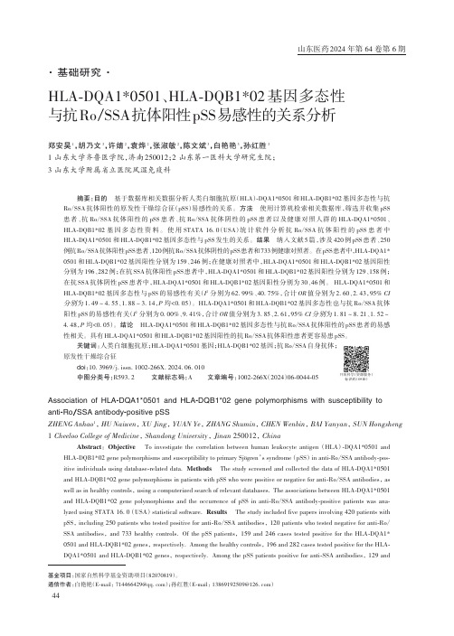
HLA -DQA1*0501、HLA -DQB1*02基因多态性与抗Ro /SSA 抗体阳性pSS 易感性的关系分析郑安昊1,胡乃文3,许婧2,袁烨2,张淑敏2,陈文斌3,白艳艳3,孙红胜31 山东大学齐鲁医学院,济南250012;2 山东第一医科大学研究生院;3 山东大学附属省立医院风湿免疫科摘要:目的 基于数据库相关数据分析人类白细胞抗原(HLA )-DQA1*0501和HLA -DQB1*02基因多态性与抗Ro /SSA 抗体阳性的原发性干燥综合征(pSS )易感性的关系。
方法 使用计算机检索相关数据库,筛选并收集pSS 患者、抗Ro /SSA 抗体阳性的pSS 患者、抗Ro /SSA 抗体阴性的pSS 患者以及健康对照人群的HLA -DQA1*0501、HLA -DQB1*02基因多态性资料。
使用STATA 16.0(USA )统计软件分析抗Ro /SSA 抗体阳性的pSS 患者中HLA -DQA1*0501和HLA -DQB1*02基因多态性与pSS 发生的关系。
结果 纳入文献5篇,涉及420例pSS 患者、250例抗Ro /SSA 抗体阳性pSS 患者、120例抗Ro /SSA 抗体阴性的pSS 患者和733例健康对照者。
在pSS 患者中,HLA -DQA1*0501和HLA -DQB1*02基因阳性分别为159、246例;在健康对照者中,HLA -DQA1*0501和HLA -DQB1*02基因阳性分别为196、282例;在抗SSA 抗体阳性pSS 患者中,HLA -DQA1*0501和HLA -DQB1*02基因阳性分别为129、158例;在抗SSA 抗体阴性pSS 患者中,HLA -DQA1*0501和HLA -DQB1*02基因阳性分别为30、46例。
HLA -DQA1*0501和HLA -DQB1*02基因多态性与pSS 的易感性有关(I 2 分别为62.99%、40.75%,合计OR 值分别为2.60、2.43,95% CI分别为1.49~4.55、1.88~3.14,P 均<0.05)。
碧云天生物技术(Beyotime Biotechnology)产品说明书

碧云天生物技术/Beyotime Biotechnology订货热线:400-168-3301或800-8283301订货e-mail:******************技术咨询:*****************网址:碧云天网站微信公众号Recombinant Murine IL-36α, 153a.a.产品编号产品名称包装P5979-2µg Recombinant Murine IL-36α, 153a.a. 2µgP5979-10µg Recombinant Murine IL-36α, 153a.a.10µgP5979-100µg Recombinant Murine IL-36α, 153a.a.100µgP5979-1mg Recombinant Murine IL-36α, 153a.a.1mg产品简介:Species Gene ID Accession Source Length MW Tag Mouse 54448 Q9JLA2 E. coli153aa 17.1kDa -About this proteinName Recombinant Murine IL-36α, 153a.a. (Recombinant Murine Interleukin-36α, 153a.a.; rMuIL-36α, 153a.a.);重组小鼠白细胞介素36α,153a.a.Synonyms FIL1 epsilon; IL-1E; IL1F6; IL36A; FIL1; FIL1 epsilon; FIL1(EPSILON); FIL1E; IL-1 epsilon; IL1(EPSILON); IL1E; IL1F6; IL-1F6; IL-1F6 (FIL-1-epsilon); interleukin 1 family, member 6 (epsilon); interleukin 1, epsilon; Interleukin 36, Alpha; Interleukin-1 epPurity >95% by SDS-PAGE and HPLC analyses.Biological Activity Fully biologically active when compared to standard. The ED50 as determined by inducing IL-6 secretion in murine NIH/3T3 cells is less than 25ng/ml, corresponding to a specific activity of >4.0×10^4IU/mg.PhysicalAppearanceSterile Filtered White lyophil ized (freeze-dried) powder.Formulation Lyophilized from a 0.2µM filtered concentrated solution in PBS, 1mM DTT, 3% trehalose. Endotoxin Less than 1EU/µg of rMuIL-36α, 153a.a. as determined by LAL method.Reconstitution We recommend that this vial be briefly centrifuged prior to opening to bring the contents to the bottom. Reconstitute in sterile distilled water or aqueous buffer containing 0.1% BSA to a concentration of0.1-1.0mg/ml. Stock solutions should be apportioned into working aliquots and stor ed at ≤-20ºC. Further dilutions should be made in appropriate buffered solutions.Category CytokineBackground Interleukin-36 (IL-36) is a pro-inflammatory cytokine which plays an important role in the pathophysiology of several diseases. IL-36α, IL-36β,and IL-36γ (formerly IL-1F6, IL-1F8, and IL-1F9) are IL-1 family members that signal through the IL-1 receptor family members IL-1Rrp2 (IL-1RL2) and IL-1RAcP. IL-36α is mainly found in skin and lymphoid tissues, but also in fetal brain, trachea, stomach a nd intestine. It is expressed by monocytes, B and T cells. Notably, IL-36 alpha is the only novel IL-1 family member expressed on T-cells. Recombinant murine interleukin-36 alpha contains 153 amino acids residues which is a single nonglycosylated polypepti de. Specifically, mouse IL-36α shares 83%a.a. sequence identity with rat IL-36α, 54-60% with human, rabbit, equine and bovine IL-36α.Amino Acid Sequence RAASPSLRHV QDLSSRVWIL QNNILTAVPR KEQTVPVTIT LLPCQYLDTL ETNRGDPTYM GVQRPMSCLF CTKDGEQPVL QLGEGNIMEM YNKKEPVKAS LFYHKKSGTT STFESAAFPG WFIAVCSKGS CPLILTQELG EIFITDFEMI VVH包装清单:产品编号产品名称包装P5979-2µg Recombinant Murine IL-36α, 153a.a.2µgP5979-10µg Recombinant Murine IL-36α, 153a.a.10µg P5979-100µg Recombinant Murine IL-36α, 153a.a.100µg P5979-1mg Recombinant Murine IL-36α, 153a.a.1mg — 说明书1份保存条件:-20ºC或更低温度保存,至少一年有效。
【CN109593881A】检测水稻低直链淀粉含量基因WxSupmqSup的KASP分子标记及方法【
(19)中华人民共和国国家知识产权局(12)发明专利申请(10)申请公布号 (43)申请公布日 (21)申请号 201910121479.7(22)申请日 2019.02.19(71)申请人 上海市农业科学院地址 201403 上海市奉贤区金齐路1000号(72)发明人 牛付安 储黄伟 曹黎明 程灿 周继华 涂荣剑 孙滨 胡雪娇 杨佳 (74)专利代理机构 杭州千克知识产权代理有限公司 33246代理人 黎双华(51)Int.Cl.C12Q 1/6895(2018.01)C12N 15/11(2006.01)(54)发明名称检测水稻低直链淀粉含量基因Wx mq 的KASP分子标记及方法(57)摘要本发明公开了一种检测水稻低直链淀粉含量基因Wx mq 的KASP分子标记及其方法,所述分子标记是根据Wx mq 基因第4外显子497bp处发生由G→A的突变而设计的,命名为Wx mq –KASP。
所述KASP标记引物包括两条正向特异性引物和一条反向通用引物。
根据本发明提供的KASP标记进行基因分型,在PCR扩增后不用酶切和电泳,可以高通量检测多个样品,快速检测Wx mq 等位基因在水稻分离群体中的分布情况,结果准确性好,与常规分子标记相比具有快捷、简便和成本较低等优点。
本发明对水稻低直链含量基因Wx mq 的分子标记辅助选择育种具有重要意义。
权利要求书1页 说明书5页序列表1页 附图1页CN 109593881 A 2019.04.09C N 109593881A权 利 要 求 书1/1页CN 109593881 A1.检测水稻低直链淀粉含量基因Wx mq的KASP分子标记,其特征在于,所述KASP分子标记(Wx mq–KASP)的引物序列为:正向引物1:5'-GATGAACACACGGTCGACTCCAT-3';正向引物2:5'-ATGAACACACGGTCGACTCCAC-3';反向通用引物:5'-GAGAGGGTGAGGTTTTTCCATTGCTA-3'。
onsemi 1SMA5913BT3 1.5瓦塑料表面贴装齐纳电压调节器 数据手册说明书
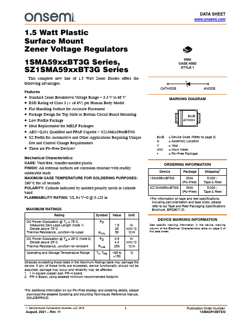
DATA SHEET 1.5 Watt PlasticSurface MountZener Voltage Regulators1SMA59xxBT3G Series,SZ1SMA59xxBT3G SeriesThis complete new line of 1.5 Watt Zener Diodes offers thefollowing advantages.Features•Standard Zener Breakdown V oltage Range − 3.3 V to 68 V•ESD Rating of Class 3 (> 16 kV) per Human Body Model•Flat Handling Surface for Accurate Placement•Package Design for Top Slide or Bottom Circuit Board Mounting•Low Profile Package•Ideal Replacement for MELF Packages•AEC−Q101 Qualified and PPAP Capable − SZ1SMA59xxBT3G•SZ Prefix for Automotive and Other Applications Requiring UniqueSite and Control Change Requirements•These are Pb−Free Devices*Mechanical Characteristics:CASE:V oid-free, transfer-molded plasticFINISH:All external surfaces are corrosion resistant with readilysolderable leadsMAXIMUM CASE TEMPERATURE FOR SOLDERING PURPOSES:260°C for 10 secondsPOLARITY:Cathode indicated by molded polarity notch or cathodebandFLAMMABILITY RATING:UL 94 V−*********MAXIMUM RATINGSRating Symbol Value UnitDC Power Dissipation @ T L = 75°C, Measured Zero Lead Length (Note 1) Derate above 75°CThermal Resistance, Junction−to−LeadP DRq JL1.52050WmW/°C°C/WDC Power Dissipation @ T A = 25°C (Note 2) Derate above 25°CThermal Resistance, Junction−to−AmbientP DR q JA0.54.0250WmW/°C°C/WOperating and Storage Temperature Range T J, T stg−65 to+150°CStresses exceeding those listed in the Maximum Ratings table may damage the device. If any of these limits are exceeded, device functionality should not be assumed, damage may occur and reliability may be affected.1. 1 in square copper pad, FR−4 board.2.FR−4 Board, using onsemi minimum recommended footprint.*For additional information on our Pb−Free strategy and soldering details, please download the onsemi Soldering and Mounting T echniques Reference Manual,SOLDERRM/D.Device Package Shipping†ORDERING INFORMATION1SMA59xxBT3G SMA(Pb−Free)5,000 /Tape & Reel†For information on tape and reel specifications, including part orientation and tape sizes, please refer to our T ape and Reel Packaging Specifications Brochure, BRD8011/D.SMACASE 403DSTYLE 1MARKING DIAGRAM8xxBAYWW G8xxB= Device Code (Refer to page 2)A= Assembly LocationY= YearWW= Work WeekG= Pb−Free PackageSee specific marking information in the device marking column of the Electrical Characteristics table on page 2 of this data sheet.DEVICE MARKING INFORMATIONSZ1SMA59xxBT3G SMA(Pb−Free)5,000 /Tape & ReelELECTRICAL CHARACTERISTICS (T A = 25°C unlessotherwise noted, V F = 1.2 V Max. @ I F = 200 mA for all types)Symbol ParameterV Z Reverse Zener Voltage @ I ZT I ZT Reverse CurrentZ ZT Maximum Zener Impedance @ I ZT I ZK Reverse CurrentZ ZK Maximum Zener Impedance @ I ZK I R Reverse Leakage Current @ V R V R Reverse Voltage I F Forward Current V F Forward Voltage @ I F I ZMMaximum DC Zener CurrentELECTRICAL CHARACTERISTICS (T A = 25°C unless otherwise noted, V F = 1.2 V Max. @ I F = 200 mA for all types)Device* (Note 3)Device Marking Zener Voltage (Note 4)Zener Impedance Leakage CurrentI ZM V Z (Volts)@ I ZT Z ZT @ I ZTZ ZK @ I ZK I R @ V R Min Nom Max mA W W mA m A Volts mA(dc)1SMA5913BT3G 813B 3.13 3.3 3.47113.610500 1.050 1.04551SMA5914BT3G 814B 3.42 3.6 3.78104.29.0500 1.035.5 1.04171SMA5915BT3G 815B 3.70 3.9 4.1096.17.5500 1.012.5 1.03851SMA5916BT3G 816B 4.08 4.3 4.5287.2 6.0500 1.0 2.5 1.03491SMA5917BT3G 817B 4.46 4.7 4.9479.8 5.0500 1.0 2.5 1.53191SMA5918BT3G 818B 4.84 5.1 5.3673.5 4.0350 1.0 2.5 2.02941SMA5919BT3G 819B 5.32 5.6 5.8866.9 2.0250 1.0 2.5 3.02681SMA5920BT3G 820B 5.89 6.2 6.5160.5 2.0200 1.0 2.5 4.02421SMA5921BT3G 821B 6.46 6.87.1455.1 2.5200 1.0 2.5 5.22211SMA5922BT3G 822B 7.127.57.8850 3.04000.5 2.5 6.02001SMA5923BT3G 823B 7.798.28.6145.7 3.54000.5 2.5 6.51831SMA5924BT3G 824B 8.649.19.5641.2 4.05000.5 2.57.01651SMA5925BT3G 825B 9.51010.537.5 4.55000.25 2.58.01501SMA5926BT3G 826B 10.451111.5534.1 5.55500.250.58.41361SMA5927BT3G 827B 11.41212.631.2 6.55500.250.59.11251SMA5928BT3G 828B 12.351313.6528.87.05500.250.59.91151SMA5929BT3G 829B 14.251515.75259.06000.250.511.41001SMA5930BT3G 830B 15.21616.823.4106000.250.512.2941SMA5931BT3G 831B 17.11818.920.8126500.250.513.7831SMA5932BT3G 832B 19202118.7146500.250.515.2751SMA5933BT3G 833B 20.92223.11717.56500.250.516.7681SMA5934BT3G 834B 22.82425.215.6197000.250.518.2631SMA5935BT3G 835B 25.652728.3513.9237000.250.520.6561SMA5936BT3G 836B 28.53031.512.5267500.250.522.8501SMA5937BT3G 837B 31.353334.6511.4338000.250.525.1451SMA5938BT3G 838B 34.23637.810.4388500.250.527.4421SMA5939BT3G 839B 37.053940.959.6459000.250.529.7381SMA5940BT3G840B40.854345.158.7539500.250.532.7351SMA5941BT3G 841B 44.654749.358.06710000.250.535.8321SMA5942BT3G 842B 48.455153.557.37011000.250.538.8291SMA5943BT3G 843B 53.25658.8 6.78613000.250.542.6271SMA5945BT3G 845B 64.66871.4 5.512017000.250.551.7223.Tolerance and Voltage Regulation Designation − The type number listed indicates a tolerance of ±5%.4.V Z limits are to be guaranteed at thermal equilibrium.*Include SZ-prefix devices where applicable.Figure 1. Steady State Power DeratingFigure 2. V Z − 3.3 thru 10 VoltsT, TEMPERATURE (°C)Figure 3. V Z = 12 thru 68 VoltsP D , M A X I M U M P O W E R D I S S I P A T I O N (W A T T S )I Z , Z E N E R C U R R E N T (m A )Z Z , DY N A M I C I M P E D A N C E (O H M S )1002468101010.1V Z , ZENER VOLTAGE (VOLTS)1001010.1010203040V Z , ZENER VOLTAGE (VOLTS)V Z , ZENER VOLTAGE (VOLTS)1001050Figure 4. Zener Voltage− 3.3 to 12 VoltsFigure 5. Zener Voltage − 12 to 68 Volts Figure 6. Effect of Zener VoltageI Z , Z E N E R C U R R E N T (m A )6070801086420-2-4V Z , ZENER VOLTAGE (VOLTS), T E M P E R A T U R E C O E F F I C I E N T (m V / C )°θV Z 10070503020101020305070100V Z , ZENER VOLTAGE (VOLTS), T E M P E R A T U R E C O E F F I C I E N T (m V / C )°θV ZFigure 7. Capacitance Curve Figure 8. Typical Pulse Rating CurveBREAKDOWN VOLTAGE (VOLTS)Figure 9. Pulse WaveformT P , PULSE WIDTH (ms)t, TIME (ms)C , C A P A C I T A N C E (p F )P p k 0.9 I 0.1 I I p p m , P E A K P U L S E, P E A K P O W E R (k W )SCALE 1:1SMA CASE 403D ISSUE JDATE 22 OCT 2021xxxx = Specific Device Code A = Assembly Location Y = YearWW = Work WeekG= Pb −Free PackageSTYLE 1:PIN 1.CATHODE (POLARITY BAND)2.ANODESTYLE 2:NO POLARITYSTYLE 1STYLE 2STYLE 1STYLE 2xxxx AYWWG xxxx AYWW G GENERICMARKING DIAGRAM**This information is generic. Please refer to device data sheet for actual part marking.Pb −Free indicator, “G” or microdot “G ”, may or may not be present. Some products maynot follow the Generic Marking.MECHANICAL CASE OUTLINEPACKAGE DIMENSIONSPUBLICATION ORDERING INFORMATIONTECHNICAL SUPPORTNorth American Technical Support:Voice Mail: 1 800−282−9855 Toll Free USA/Canada Phone: 011 421 33 790 2910LITERATURE FULFILLMENT :Email Requests to:*******************onsemi Website: Europe, Middle East and Africa Technical Support:Phone: 00421 33 790 2910For additional information, please contact your local Sales Representative。
柔木丹改善小鼠肝纤维化的TGF-β1/Smad4信号通路机制
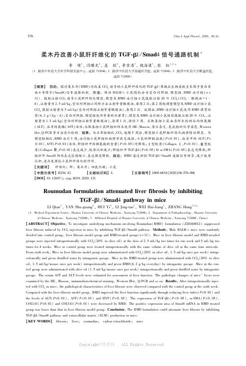
柔木丹改善小鼠肝纤维化的TGF β1/Smad4信号通路机制 李 倩1,闫曙光2,惠 毅2,李京涛3,魏海梁3,张 红1,2△(1.陕西中医药大学医学科研实验中心,咸阳712046;2.陕西中医药大学基础医学院,咸阳712046;3.陕西中医药大学附属医院,咸阳712000)【摘要】 目的:探讨柔木丹(RMD)对改善CCl4诱导的小鼠肝纤维化的TGF β1/果蝇抗生物皮肤生长因子蛋白家族4号因子(Smad4)信号通路机制。
方法:雄性BALB/c小鼠随机分为空白对照组、模型组、RMD治疗组(n=11)。
腹腔注射CCl4诱导小鼠肝纤维化模型,模型及RMD治疗组小鼠腹腔注射20%CCl4(CCl4∶橄榄油=1∶4),注射量为2.5ml/kg,空白对照组以同样方法注射等量橄榄油,每周2次;第2周起调整模型及RMD治疗组小鼠CCl4腹腔注射量为5ml/kg(空白对照组注射等量橄榄油),每周2次。
成模后,RMD治疗组小鼠使用RMD灌胃给药(6.2g/(kg·d);空白对照组、模型组使用等量的水灌胃),模型及RMD治疗组小鼠继续腹腔注射20%CCl4,注射量为1.5ml/kg(空白对照组注射等量橄榄油),每周1次,持续3周。
采取各组小鼠血清样本检测谷丙转氨酶(ALT)、谷草转氨酶(AST)活性;采取各组小鼠肝组织样本使用HE、Masson、原位杂交、免疫组织化学染色、Westernblot、Q PCR等方法进行检测。
结果:与正常组相比,CCl4造模5周后,模型组小鼠肝脏纤维化病理特征明显。
与模型组相比,RMD治疗3周,治疗组小鼠肝组织病理学改变减轻,小鼠的肝脏指数(P<0.01)、血清中的ALT(P<0.01)、AST(P<0.01)活性、肝组织中羟脯氨酸的含量(P<0.05)均降低;Ⅰ型胶原(CollagenⅠ,P<0.01)、Ⅲ型胶原(CollagenⅢ,P<0.01)表达减少,胶原沉积减少;肝组织中TGF β1(P<0.05)和α SMA(P<0.05)表达均降低;肝组织中Smad4阳性表达区域缩小、表达强度降低。
临床常用免疫组化指标

常用免疫组化指标的意义Ki-67为细胞增殖的一种标记,在细胞周期G1、S、G2、M期均有表达,G0期缺如,其和许多肿瘤分化程度、浸润、转移、预后密切相关。
PCNA(增殖细胞核抗原)。
多数腺癌表达CEARb (retinoblastoma视网膜母细胞瘤)基因是肿瘤抑制基因,调节细胞周期。
P53在免疫组化中均为突变型,阳性率越高,预后约差。
野生型半衰期很短Nm23是转移抑制基因,其阳性表达和肿瘤转移呈负相关。
E-Ca E钙粘附蛋白,介导细胞间粘连作用的跨膜糖蛋白,其功能丧失引起细胞之间连接的破坏,主要用于肿瘤侵袭和转移方面的研究.PS2 (雌激素调节蛋白),其表达和ER表达有关,可作为内分泌治疗和预后判断的指标之一。
CK18 低分子量角蛋白,主要标记各种单层上皮包括腺上皮,而复层鳞状上皮常阴性,主要用于腺癌诊断。
CK19 分布于单层上皮和间皮,常用于腺癌诊断,肝细胞不表达,而胆管为阳性反应Hep par 肝细胞抗原,正常肝细胞和高分化肝细胞癌阳性,低分化肝细胞癌多弱阳性或阴性.CK20 用于胃肠道腺癌、卵巢黏液性肿瘤、皮肤Merkel细胞癌诊断。
鳞癌、乳腺癌、肺癌、子宫内膜和卵巢非黏液性肿瘤常阴性。
CK7 卵巢、肺和乳腺上皮常阳性,结肠、前列腺、胃肠道上皮阴性.Villin 绒毛蛋白,正常组织中,villin通常只表达于有刷状缘的细胞上,如胃肠道上皮细胞、胰腺和胆管上皮细胞以及肾实质的上皮细胞中(特别是近曲小管)。
Villin在胃肠道癌、胰腺癌、胆囊癌和胆管癌组织中有很高的表达率,具有明显腺样结构的肿瘤上没有villin表达,则这个肿瘤为胃肠道、胰腺、胆囊或胆管来源的可能性极低.乳腺癌也经常成为女性患者未知原发部位转移癌要鉴别排除的一种疾病。
因为在转移癌组织上观察到明显的villin免疫组化阳性染色,则这个肿瘤就极不可能为乳腺来源.其他villin免疫组化染色通常为阴性表达的肿瘤还有:如卵巢浆液性癌、尿道移行细胞癌和前列腺癌。
- 1、下载文档前请自行甄别文档内容的完整性,平台不提供额外的编辑、内容补充、找答案等附加服务。
- 2、"仅部分预览"的文档,不可在线预览部分如存在完整性等问题,可反馈申请退款(可完整预览的文档不适用该条件!)。
- 3、如文档侵犯您的权益,请联系客服反馈,我们会尽快为您处理(人工客服工作时间:9:00-18:30)。
OVZ, TEMPERATURE COEFFICIENT (mV/oC)
FIG.4- EFFECT OF ZENER VOLTAGE
ZZ, DYNAMIC IMPEDANCE (OHMS)
VZ @ IZ1
100
IZ(dc) = 1 mA
10
10 mA IZ(ms) = 0.1 IZ(dc)
100
Rating at 25+ambient temperature unless otherwise specified. Type Number DC Power Dissipation at TL=75OC, measure at Zero Lead Length (Note 1) Derate 128 -
ELECTRICAL CHARACTERISTICS
(TA=25OC unless otherwise noted) VF=1.5V max, IF=200mA for all types.
Nominal Device Zener Voltage Test Zener Impedance Marking Vz @ Izt Current ZZK @ IZK Code Voltage IZT ZZT @ IZT (Notes 2) mA Ohms Ohms mA
1
100
0.1
TJ = 25 C
10 10
BREAKDOWN VOLTAGE (VOLTS)
o
100
0.01
0.01
0.1
Tp, PULSE WIDTH (ms)
1
10
FIG.7- PULSE WAVEFORM
120 120
FIG.8- PULSE WAVEFORM
10 s
Ippm, PEAK PULSE CURRENT (%)
.187(4.75) .167(4.25)
Mechanical Data
a a a a Case: Molded plastic over passivated junction Terminals: Solder plated, solderable per MIL-STD-750, Method 2026 Polarity: Color Band denotes positive end (cathode) Standard packaging: 12mm tape (EIA-481)
926A 927A 928A 929A 930A 931A 932A 933A 934A 935A 936A 937A 938A 939A 940A 941A 942A 943A 944A 945A 11 12 13 15 16 18 20 22 24 27 30 33 36 39 43 47 51 56 62 68 34.1 31.2 28.8 25.0 23.4 20.8 18.7 17.0 15.6 13.9 12.5 11.4 10.4 9.6 8.7 8.0 7.3 6.7 6.0 5.5 5.5 6.5 7.0 9.0 10.0 12 14 17.5 19 23 26 33 38 45 53 67 70 86 100 120.0 550 550 550 600 600 650 650 650 700 700 750 800 850 900 950 1000 1100 1300 1500 1700 0.25 0.25 0.25 0.25 0.25 0.25 0.25 0.25 0.25 0.25 0.25 0.25 0.25 0.25 0.25 0.25 0.25 0.25 0.25 0.25
100
Ippm, PEAK PULSE CURRENT (%)
80
PEAK VALUE Ippm
TA = 25oC PW (ID) IS DEFINED AS THE POINT WHERE THE PEAK CURRENT DECAYS TO 50% OF Ipp-
100
0.9 IPEAK
80
8/20 s WAVEFORM AS DEFINED BY ANSI C62.1 AND IEC 801-5,
T 20 s
- 131 -
Device (Note 1)
1SMA5926 1SMA5927 1SMA5928 1SMA5929 1SMA5930 1SMA5931 1SMA5932 1SMA5933 1SMA5934 1SMA5935 1SMA5936 1SMA5937 1SMA5938 1SMA5939 1SMA5940 1SMA5941 1SMA5942 1SMA5943 1SMA5944 1SMA5945
Maximum DC Zener Leakage Current Current IR @ VR IZM uA Volts mA (dc)
0.5 0.5 0.5 0.5 0.5 0.5 0.5 0.5 0.5 0.5 0.5 0.5 0.5 0.5 0.5 0.5 0.5 0.5 0.5 0.5 8.4 9.1 9.9 11.4 12.2 13.7 15.2 16.7 18.2 20.6 22.8 25.1 27.4 29.7 32.7 35.8 38.8 42.6 47.1 51.7 136 125 115 100 94 83 75 68 63 56 50 45 42 38 35 32 29 27 24 22
2
Symbol PD
Value 1.5 20
Units Watts mW/ OC
IFSM
10.0
Amps
O
TJ, TSTG -55 to + 150 Notes: 1. Mounted on 5.0mm (0.013mm thick) land areas. 2. Measured on 8.3ms Single Half Sine-wave or Equivalent Square Wave, Duty Cycle=4 Pulses Per Minute Maximum.
100
3.2
IZ, ZENER CURRENT (mA)
2.4
10
TL
1.6
1
0.8
TA
0 0 25 50 75
o
100
125
150
0.1 0 10 20
VZ, ZENER VOLTAGE (VOLTS)
T, TEMPERATURE( C)
30
40
50
60
70
80
FIG.3- ZENER VOLTAGE - 14 TO 68 VOLTS
1SMA5926 THRU 1SMA5945
Surface Mount Silicon Zener Diode
Voltage Range 11 to 68 Volts 1.5 Watts Peak Power
Features
a a a a a a a
a
SMA/DO-214AC
.062(1.58) .056(1.43) .111(2.83) .102(2.29)
For surface mounted applications in order to optimize board space Low profile package Built-in strain relief Glass passivated junction Low inductance Typical IR less than 0.5 A above 11V High temperature soldering guaranteed: 260OC / 10 seconds at terminals Plastic package has Underwriters Laboratory Flammability Classification 94V-0
Peak Forward Surge Current, 8.3 ms Single Half Sine-wave Superimposed on Rated Load (JEDEC method) (Note 1, 2) Operating and Storage Temperature Range
VZ, ZENER VOLTAGE (VOLTS)
20 mA
10
10 10
VZ, ZENER VOLTAGE (VOLTS)
100
- 130 -
RATINGS AND CHARACTERISTIC CURVES ( 1SMA5926 THRU 1SMA5945)
FIG.5- CAPACITANCE CURVE
1000
FIG.6- TYPICAL PULSE RATING CURVE
10
PPK, PEAK POWER (kW)
C, CAPACITANCE (pF)
MEASURED @ ZERO BIAS MEASURED @ VZ/2
NONREPETITIVE, EXPONENTIAL o PULSE WAVEFORM, TJ = 25 C
Notes: 1: Tolerance and Voltage Regulation Designation - the type number listed indicates a tolerance of ±5%. 2: VZ limits are to be guaranteed at thermal equilibrium.
60
60
HALF VALUE - Ipp/2
0.5 IPEAK
40
40
10/1000 s WAVEFORM AS DEFINED BY R.E.A. td 0.1 IPEAK
1 2
t, TIME (ms)
20
20
T=8 s
0 0 0.02 0.04
