HT2801规格书新
28015;中文规格书,Datasheet资料
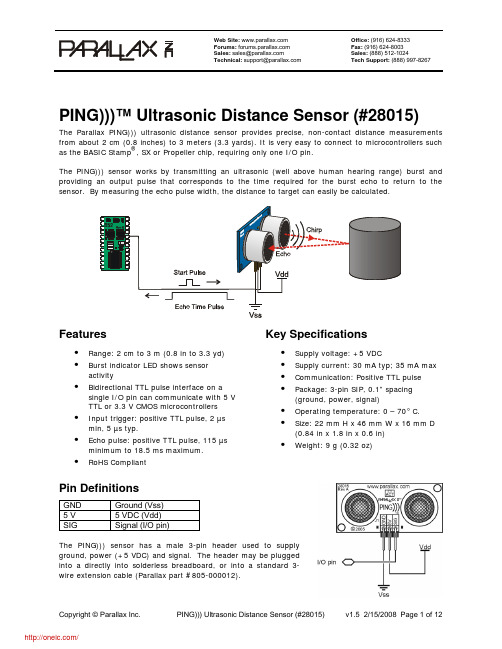
The percent error over the sensor’s operating range of 0 to 70 ° C is significant, in the magnitude of 11 to 12 percent. The use of conversion constants to account for air temperature may be incorporated into your program (as is the case in the example BS2 program given in the Example Programs section below). Percent error and conversion constant calculations are introduced in Chapter 2 of Smart Sensors and Applications, a Stamps in Class text available for download from the 28029 product page at .
v1.5 2/15/2008 Fra bibliotekage 2 of 12
Practical Considerations for Use
Object Positioning
The PING))) sensor cannot accurately measure the distance to an object that: a) is more than 3 meters away, b) that has its reflective surface at a shallow angle so that sound will not be reflected back towards the sensor, or c) is too small to reflect enough sound back to the sensor. In addition, if your PING))) sensor is mounted low on your device, you may detect sound reflecting off of the floor. a. b. c.
光耦资料PS2801
DATA SHEETThe information in this document is subject to change without notice. Document No. P12277EJ6V0DS00 (6th edition)Date Published May 1998 NS CP(K) Printed in Japan©1991 The mark • shows major revised points.DESCRIPTIONThe PS2801-1 and PS2801-4 are optically coupled isolators containing a GaAs light emitting diode and an NPN silicon phototransistor in a plastic SOP for high density applications.This package has shield effect to cut off ambient light.FEATURES•High isolation voltage (BV = 2 500 Vr.m.s.)•Small and thin package (4,16-pin SOP, Pin pitch 1.27 mm)•High collector to emitter voltage (V CEO = 80 V)•High-speed switching (t r = 3 µs TYP., t f = 5 µs TYP.)•UL approved: File No. E72422 (S)•VDE0884 approved (Option): PS2801-4 only•Operating number of taping product: PS2801-1-F3, F4, PS2801-4-F3, F4APPLICATIONS•Programmable logic controllers•Measuring instruments•Power supply•Hybrid ICPACKAGE DIMENSIONS (in millimeters)MARKING2ABSOLUTE MAXIMUM RATINGS (T A = 25 °C, unless otherwise specified)Parameter Symbol Ratings UnitPS2801-1PS2801-4Diode Forward Current (DC)I F50mAReverse Voltage V R6VPower Dissipation Derating∆P D/°C0.60.8mW/°CPower Dissipation P D6080mW/chPeak Forward Current*1I FP1ATransistor Collector to Emitter Voltage V CEO80VEmitter to Collector Voltage V ECO6VCollector Current I C50mA/chPower Dissipation Derating∆P C/°C 1.2mW/°CPower Dissipation P C120mW/chIsolation Voltage*2BV 2 500Vr.m.s.Operating Ambient Temperature T A−55 to +100°CStorage Temperature T stg−55 to +150°C*1PW = 100 µs, Duty Cycle = 1 %*2AC voltage for 1 minute at T A = 25 °C, RH = 60 % between input and output3ELECTRICAL CHARACTERISTICS (T A = 25 °C)Parameter Symbol Conditions MIN.TYP.MAX.UnitDiode Forward Voltage V F I F = 5 mA1.1 1.4VReverse Current I R V R = 5 V5µATerminal Capacitance C t V = 0 V, f = 1.0 MHz30pF Transistor Collector to EmitterDark CurrentI CEO V CE = 80 V, I F = 0 mA100nACoupled Current Transfer Ratio(I C/I F)CTR I F = 5 mA, V CE = 5 V80600%Collector SaturationVoltageV CE(sat)I F = 10 mA, I C = 2 mA0.3V Isolation Resistance R I-O V I-O = 1.0 kV DC1011ΩIsolation Capacitance C I-O V = 0 V, f = 1.0 MHz0.4pFRise Time*1t r V CC = 5 V, I C = 2 mA, R L = 100 Ω3µsFall Time*1t f5 *1Test circuit for switching timeV CC45TYPICAL CHARACTERISTICS (T A = 25 °C, unless otherwise specified)Ambient Temperature T A (˚C)D i o d e P o w e r D i s s i p a t i o n P D (m W )DIODE POWER DISSIPATION vs.AMBIENT TEMPERATUREAmbient Temperature T A ( ˚C)T r a ns i s t o r P o w e r D i s s i p a t i o n P C (m W )TRANSISTOR POWER DISSIPATION vs. AMBIENT TEMPERATUREForward Voltage V F (V)F o r w a r d C u r r e n t I F (m A )FORWARD CURRENT vs.FORWARD VOLTAGECollector to Emitter Voltage V CE (V)C o l l e c t o r C u r r e n t I C (m A )COLLECTOR CURRENT vs.COLLECTOR TO EMITTER VOLTAGEAmbient Temperature T A (˚C)C o l l e c t o r t o E m i t t er D a r k C u r r e n t I C E O (n A )COLLECTOR TO EMITTER DARKCURRENT vs. AMBIENT TEMPERATURECollector Saturation Voltage V CE(sat) (V)C o l l e c t o r C u r r e n t I C (m A )COLLECTOR CURRENT vs.COLLECTOR SATURATION VOLTAGE6FREQUENCY RESPONSEFrequency f (kHz)NormalizedGainGvLONG TERM CTR DEGRADATIONTime (Hr)CTR(RelativeValue)V CE = 5 V,n = 30.021000.1 1.01010020050150250300Forward Current I F (mA)CurrentTransferRatioCTR(%)CURRENT TRANSFER RATIO vs.FORWARD CURRENTNormalized to 1.0at T A = 25 ˚C,I F = 5 mA, V CE = 5 V,,,,,,,,,,,,,,,,,,,,,,,,,,,,,,,,,,,,,,,,,,,,,,,,,,,,,,,,,,,,,,,,,,,,,,,,,,,–500100–252550750.00.61.20.20.41.00.8Ambient Temperature T A (˚C)NormalizedCurrentTransferRatioCTRNORMALIZED CURRENT TRANSFERRATIO vs. AMBIENT TEMPERATURESwitchingTimet(s)µLoad Resistance R L (kΩ)SWITCHING TIME vs.LOAD RESISTANCELoad Resistance R L (kΩ)SWITCHING TIME vs.LOAD RESISTANCESwitchingTimet(s)µRemark The graphs indicate nominal characteristics.TAPING SPECIFICATIONS (in millimeters)PS2801-17PS2801-489RECOMMENDED SOLDERING CONDITIONS(1) Infrared reflow soldering •Peak reflow temperature235 °C (package surface temperature)•Time of temperature higher than 210 °C 30 seconds or less •Number of reflows Three•FluxRosin flux containing small amount of chlorine (The flux with a maximum chlorine content of 0.2 Wt % is recommended.)P a c k ag e S u r f a c e T e m p e r a t u r e T (˚C )Time (s)Recommended Temperature Profile of Infrared ReflowCaution Avoid removing the residual flux with chlorine-based cleaning solvent after a reflow process.(2) Dip soldering •Temperature 260 °C or below (molten solder temperature)•Time10 seconds or less •Number of times One•FluxRosin flux containing small amount of chlorine (The flux with a maximum chlorine content of 0.2 Wt % is recommended.)PROGRAMMABLE LOGIC CONTROLLERS EXAMPLE Purpose: In-out interface10[MEMO]11CAUTIONWithin this device there exists GaAs (Gallium Arsenide) material which is aharmful substance if ingested. Please do not under any circumstances break thehermetic seal.NEPOC is a trademark of NEC Corporation.No part of this document may be copied or reproduced in any form or by any means without the prior written consent of NEC Corporation. NEC Corporation assumes no responsibility for any errors which may appear in this document.NEC Corporation does not assume any liability for infringement of patents, copyrights or other intellectual property rights of third parties by or arising from use of a device described herein or any other liability arising from use of such device. No license, either express, implied or otherwise, is granted under any patents, copyrights or other intellectual property rights of NEC Corporation or others.While NEC Corporation has been making continuous effort to enhance the reliability of its semiconductor devices, the possibility of defects cannot be eliminated entirely. To minimize risks of damage or injury to persons or property arising from a defect in an NEC semiconductor device, customers must incorporate sufficient safety measures in its design, such as redundancy, fire-containment, and anti-failure features.NEC devices are classified into the following three quality grades:"Standard", "Special", and "Specific". The Specific quality grade applies only to devices developed based on a customer designated "quality assurance program" for a specific application. The recommended applications of a device depend on its quality grade, as indicated below. Customers must check the quality grade of each device before using it in a particular application.Standard: Computers, office equipment, communications equipment, test and measurement equipment, audio and visual equipment, home electronic appliances, machine tools, personal electronicequipment and industrial robotsSpecial: Transportation equipment (automobiles, trains, ships, etc.), traffic control systems, anti-disaster systems, anti-crime systems, safety equipment and medical equipment (not specifically designedfor life support)Specific: Aircrafts, aerospace equipment, submersible repeaters, nuclear reactor control systems, life support systems or medical equipment for life support, etc.The quality grade of NEC devices is "Standard" unless otherwise specified in NEC's Data Sheets or Data Books. If customers intend to use NEC devices for applications other than those specified for Standard quality grade, they should contact an NEC sales representative in advance.Anti-radioactive design is not implemented in this product.M4 96. 5。
福士科铸造涂料产品说明书
福士科铸造涂料产品说明书全文共四篇示例,供读者参考第一篇示例:【福士科铸造涂料产品说明书】一、产品简介福士科铸造涂料是一种专为金属铸造领域设计的高性能涂料,具有优良的耐热性、耐磨性和耐腐蚀性。
该涂料采用先进的技术配方,具有优异的抗高温性能,能有效提高金属铸造件的表面质量和使用寿命。
福士科铸造涂料涂布均匀,易于涂抹,能够有效遮盖铸造件表面的缺陷,提高铸造件的整体质量和外观。
二、产品特点1. 高耐热性:福士科铸造涂料采用特殊的热稳定配方,能够在高温环境下保持良好的性能,不会出现脱落、开裂等问题。
2. 耐磨性强:该涂料具有良好的耐磨性能,能够有效保护铸造件表面,延长使用寿命。
3. 耐腐蚀性好:福士科铸造涂料具有优异的耐腐蚀性能,能够抵抗酸碱及其他腐蚀物质的侵蚀。
4. 易涂抹:该涂料涂布均匀,易于涂抹,操作简便。
5. 改善铸造件表面质量:能够有效遮盖铸造件表面的缺陷,提高铸造件的整体质量和外观,减少二次修磨的工序。
三、适用范围福士科铸造涂料适用于各种金属铸造领域,包括铁、铝、铜等金属铸造件的涂料保护。
常用于汽车零部件、工程机械、管道、阀门等领域的铸造件表面处理。
四、使用方法1. 准备工作:将铸造件表面清洁干净,确保无油污、灰尘等,保证涂料可以充分附着在表面上。
2. 搅拌均匀:将涂料倒入容器中,进行充分搅拌,确保配方各部分充分混合均匀。
3. 涂抹处理:使用刷子、喷枪等工具将涂料涂抹在铸造件表面上,使每个部位均匀涂覆。
4. 干燥固化:让涂料自然风干或者采用加热固化的方式,使其充分干燥固化。
5. 检查修整:对涂好的铸造件进行检查,如有需要可进行修整处理。
五、注意事项1. 福士科铸造涂料仅限于金属铸造件表面处理,不得用于其他材料的处理。
2. 使用涂料前请充分阅读产品说明书,并遵循正确的使用方法。
3. 在操作过程中请做好安全防护措施,避免直接接触皮肤和眼睛。
4. 存放时请放置在阴凉干燥处,防止受潮和曝晒。
5. 本产品属于易燃品,请远离明火和火源。
HT 规格书
•低压降•较低的温度系数•高输入电压 (高达 30V)•静态电流 2.5μA•大电流输出:100mA•输出电压精度:±3%•封装类型:TO92, SOT89 和 SOT23-5应用领域•电池供电设备•通信设备•音频/视频设备功耗高电压稳压器。
输出电流为 100mA 且允许的输入电压可高达 30V。
具有几个固定的输出电压,范围从 2.1V 到 12.0V。
CMOS 技术可确保其具有低压降和低静态电流的特性。
尽管主要为固定电压调节器而设计,但这些 IC 可与外部元件结合来获得可变的电压和电流。
注:“xx”代表输出电压。
Rev. 2.3012014-03-19引脚图极限参数工作环境温度 .................................................−40°C ~ 85°C 电源供应电压 ...................................................−0.3V ~ 33V储存温度范围 ...............................................−50°C ~ 125°C注:这里只强调额定功率,超过极限参数所规定的范围将对芯片造成损害,无法预期芯片在上述标示范围外的工作状态,而且若长期在标示范围外的条件下工作,可能影响芯片的可靠性。
热能信息Rev. 2.3022014-03-19电气特性HT7521-1, +2.1V 输出类型注:在 V IN = V OUT+2V 与一个固定负载条件下使输出电压下降 2%,此时的输入电压减去输出电压就是Dropout 电压。
HT7523-1, +2.3V 输出类型注:在 V IN = V OUT+2V 与一个固定负载条件下使输出电压下降 2%,此时的输入电压减去输出电压就是Dropout 电压。
Rev. 2.3032014-03-19注:在 V IN = V OUT+2V 与一个固定负载条件下使输出电压下降 2%,此时的输入电压减去输出电压就是Dropout 电压。
AON2801;中文规格书,Datasheet资料
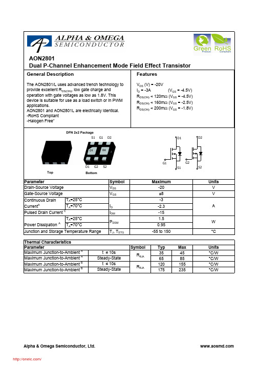
Symbol V DS SymbolTyp Max 35456585120155175235Maximum Junction-to-Ambient A t ≤ 10s R θJA °C/W Maximum Junction-to-Ambient A Steady-State °C/W Units ParameterDrain-Source Voltage Thermal Characteristics ParameterUnits Maximum Junction-to-Ambient B t ≤ 10s R θJA °C/W Maximum Junction-to-Ambient BSteady-State°C/WAON2801Dual P-Channel Enhancement Mode Field Effect TransistorGeneral DescriptionThe AON2801/L uses advanced trench technology to provide excellent R DS(ON), low gate charge and D2S2TopBottomS2D1G2SymbolMin TypMaxUnits BV DSS -20V -1T J =55°C-5I GSS ±100nA V GS(th)-0.3-0.55-1V I D(ON)-15A 100120T J =125°C135170128160m Ω160200m Ωg FS 6S V SD -0.76V I S-1A C iss 540700pF C oss 90pF C rss 63pF R g9.5ΩQ g 56.5nC Q gs 1.2nC Q gd 1nC t D(on)5ns t r 40ns t D(off)28.5ns t f46ns t rr 2128ns Q rr9.1nC-15THIS PRODUCT HAS BEEN DESIGNED AND QUALIFIED FOR THE CONSUMER MARKET. APPLICATIONS OR USES AS CRITICAL COMPONENTS IN LIFE SUPPORT DEVICES OR SYSTEMS ARE NOT AUTHORIZED. AOS DOES NOT ASSUME ANY LIABILITY ARISING OUT OF SUCH APPLICATIONS OR USES OF ITS PRODUCTS. AOS RESERVES THE RIGHT TO IMPROVE PRODUCT DESIGN,FUNCTIONS AND RELIABILITY WITHOUT NOTICEParameter Conditions STATIC PARAMETERS Electrical Characteristics (T J =25°C unless otherwise noted)Drain-Source Breakdown Voltage I D =-250µA, V GS =0V I DSS Zero Gate Voltage Drain Current V DS =-20V, V GS =0VµA Gate-Body leakage current V DS =0V, V GS =±8V Gate Threshold Voltage V DS =V GS I D =-250µA On state drain currentV GS =-4.5V, V DS =-5V R DS(ON)Static Drain-Source On-ResistanceV GS =-4.5V, I D =-3Am ΩV GS =-2.5V, I D =-2.6A V GS =-1.8V, I D =-1.5AForward Transconductance V DS =-5V, I D =-3A Diode Forward VoltageI S =-1A,V GS =0VMaximum Body-Diode Continuous CurrentDYNAMIC PARAMETERS Input Capacitance V GS =0V, V DS =-10V, f=1MHz Output CapacitanceReverse Transfer Capacitance Gate resistanceV GS =0V, V DS =0V, f=1MHzSWITCHING PARAMETERSTotal Gate Charge V GS =-4.5V, V DS =-10V, I D =-3AGate Source Charge Gate Drain Charge Turn-On DelayTime V GS =-4.5V, V DS =-10V, R L =1.5Ω,R GEN =3ΩTurn-On Rise Time Turn-Off DelayTime Turn-Off Fall TimeBody Diode Reverse Recovery TimeI F =-3A, dI/dt=100A/µsBody Diode Reverse Recovery Charge I F =-3A, dI/dt=100A/µsA: The value of R θJA is measured with the device mounted on 1in 2 FR-4 board with 2oz. Copper, in a still air environment with T A =25°C. ThePower dissipation P DSM is based on R θJA and the maximum allowed junction temperature of 150°C. The value in any given application dependson the user's specific board design, and the maximum temperature of 150°C may be used if the PCB allows it to.B. The value of R θJA is measured with the device mounted on a minimum pad board with 2oz. Copper, in a still air environment with T A =25°C.The Power dissipation P DSM is based on R θJA and the maximum allowed junction temperature of 150°C. The value in any given application depends on the user's specific board design, and the maximum temperature of 150°C may be used if the PCB allows it to.C. The R θJA is the sum of the thermal impedence from junction to case R θJC and case to ambient.D. The static characteristics in Figures 1 to 6 are obtained using <300 µs pulses, duty cycle 0.5% max.E. These tests are performed with the device mounted on 1 in 2 FR-4 board with 2oz. Copper, in a still air environment with T A =25°C. The SOA curve provides a single pulse rating.*This device is guaranteed green after data code 7111 (Oct 15 2007).Rev 2: Sep 2008VdsChargeGate Charge Test Circuit & WaveformVdd VddResistive Switching Test Circuit & W aveforms90%10%分销商库存信息: AOSAON2801。
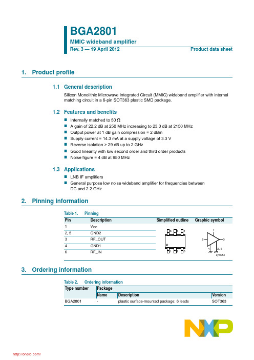
BGA2801,115;中文规格书,Datasheet资料
Max 3.6 16.3 22.8 23.1 24.4 19 19 19 22 16 15
Unit V mA dB dB dB dB dB dB dB dB dB
2 of 18
© NXP B.V. 2012. All rights reserved.
Product data sheet
Rev. 3 — 19 April 2012
BGA2801
MMIC wideband amplifier
Rev. 3 — 19 April 2012 Product data sheet
1. Product profile
1.1 General description
Silicon Monolithic Microwave Integrated Circuit (MMIC) wideband amplifier with internal matching circuit in a 6-pin SOT363 plastic SMD package.
6. Thermal characteristics
Table 5. Symbol Rth(j-sp) Thermal characteristics Parameter Conditions Typ 300 Unit K/W thermal resistance from junction to Ptot = 200 mW; Tsp = 90 C solder point
/
NXP Semiconductors
BGA2801
MMIC wideband amplifier
Table 6. Characteristics …continued VCC = 3.3 V; ZS = ZL = 50 ; Pi = 30 dBm; Tamb = 25 C; measured on demo board; unless otherwise specified. Symbol Parameter ISL isolation Conditions f = 250 MHz f = 950 MHz f = 2150 MHz NF noise figure f = 250 MHz f = 950 MHz f = 2150 MHz B3dB K 3 dB bandwidth Rollett stability factor 3 dB below gain at 1 GHz f = 250 MHz f = 950 MHz f = 2150 MHz PL(sat) saturated output power f = 250 MHz f = 950 MHz f = 2150 MHz PL(1dB) output power at 1 dB gain compression f = 250 MHz f = 950 MHz f = 2150 MHz IP3I input third-order intercept point Pdrive = 34 dBm (for each tone) f1 = 250 MHz; f2 = 251 MHz f1 = 950 MHz; f2 = 951 MHz f1 = 2150 MHz; f2 = 2151 MHz IP3O output third-order intercept point Pdrive = 34 dBm (for each tone) f1 = 250 MHz; f2 = 251 MHz f1 = 950 MHz; f2 = 951 MHz f1 = 2150 MHz; f2 = 2151 MHz PL(2H) second harmonic output power Pdrive = 31 dBm f1H = 250 MHz; f2H = 500 MHz f1H = 950 MHz; f2H = 1900 MHz IM2 second-order intermodulation distance Pdrive = 34 dBm (for each tone) f1 = 250 MHz; f2 = 251 MHz f1 = 950 MHz; f2 = 951 MHz 34 27 45 39 56 50 dBc dBc 62 51 60 50 58 48 dBm dBm 12 12 6 14 14 9 16 16 13 dBm dBm dBm 10 11 17 8 8 14 6 6 10 dBm dBm dBm Min 58 46 29 3.4 3.4 3.5 2.5 252 7 0.7 4 2 1 1 0 1 Typ 78 47 32 3.8 3.8 3.9 2.8 308 8 1.3 4 4 2 2 2 0 Max 99 49 34 4.3 4.3 4.4 3.1 363 10 1.9 5 5 3 3 3 1 dBm dBm dBm dBm dBm dBm Unit dB dB dB dB dB dB GHz
JIS_Z_2801中文
JIS_Z_2801:2000_Antimicrobial_products_--_Test_for_antimicrobial概要本规格是在工业标准化的基础上,经过日本工业标准调查会的审查,由通商产业大臣制定的日本工业规格。
日本工业标准-----抗菌加工产品-抗菌试验方法,抗菌效果序文:与生活相关的新功能加工产品座谈会记录:平成10年12月在所谓的抗菌加工指示书上表示,本规格是为了对抗菌加工产品抗菌效果的评价方法规范化而制定的日本工业规格。
但是,本规格只是对抗菌加工产品及其重要的抗菌效果及试验方法做的规定,对其安全性,抗菌效果的持续性等等请参照“抗菌加工产品指示书”。
1、试用范围本规格是针对抗菌加工产品(含中间产品)表面细菌的抗菌性试验方法及抗菌效果的规定。
2、参考文件下列标准和条款通过本标准的引用成为本标准,版本更新的标准适用本标准。
JIS K0950 塑料杀菌碟JIS K0970 按钮式液体用微量体积计JIS K3800 二级的生物安全装置JIS K8101 乙醇(99.5)(试剂)JIS K8150 盐酸JIS K8180 盐酸(试剂)JIS K8263 琼脂(试剂)JIS K8576 氢氧化钠(试剂)JIS K9007 磷酸二氢钾JIS K9017 磷酸二钾JIS K9012纺织产品的抗菌性实验方法JLS R3505 玻璃材质的体积计3、定义本标准使用了如下定义和术语A)抗菌抑制产品表面细菌繁殖B)杀菌抗菌的最终效果Page 1 / Total 8JIS_Z_2801:2000_Antimicrobial_products_--_Test_for_antimicrobialC)抗菌产品进行抗菌加工的产品D)抗菌活性值加工产品和未加工产品进行细菌接种培养后的细菌数进行对比后的差值《参考 JIS L1902 抗菌活性值评估与判定》E)抗菌效果从抗菌活性值判断抗菌加工产品的效果4、抗菌效果抗菌加工产品的抗菌效果,根据本规格的试验方法得出,抗菌活性值为2.0以上。
ULN2801A中文资料
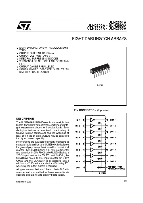
ULN2801AULN2804A - ULN2805AULN2802A - ULN2803A September 2003EIGHT DARLINGTON ARRAYS®.EIGHT DARLINGTONS WITH COMMON EMIT-TERS.OUTPUT CURRENT TO 500 mA .OUTPUT VOLTAGE TO 50 V.INTEGRAL SUPPRESSION DIODES.VERSIONS FOR ALL POPULAR LOGIC FAMI-LIES.OUTPUT CAN BE PARALLELED.INPUTS PINNED OPPOSITE OUTPUTS TO SIMPLIFY BOARD LAYOUTDESCRIPTIONThe ULN2801A-ULN2805A each contain eight dar-lington transistors with common emitters and inte-gral suppression diodes for inductive loads. Each darlington features a peak load current rating of 600mA (500mA continuous) and can withstand at least 50V in the off state. Outputs may be paralleled for higher current capability.Five versions are available to simplify interfacing to standard logic families : the ULN2801A is designed for general purpose applications with a current limit resistor ; the ULN2802A has a 10.5k Ω input resistor and zener for 14-25V PMOS ; the ULN2803A has a 2.7k Ω input resistor for 5V TTL and CMOS ; the ULN2804A has a 10.5k Ω input resistor for 6-15V CMOS and the ULN2805A is designed to sink a minimum of 350mA for standard and Schottky TTL where higher output current is required.All types are supplied in a 18-lead plastic DIP with a copper lead from and feature the convenient input-opposite-output pinout to simplify board layout.DIP18PIN CONNECTION (top view)1/8SCHEMATIC DIAGRAM AND ORDER CODESFor ULN2801A (each driver for PMOS-CMOS)For ULN2802A (each driver for 14-15 V PMOS)For ULN2803A (each driver for 5 V, TTL/CMOS)For ULN2804A (each driver for 6-15 VCMOS/PMOSFor ULN2805A (each driver for high out TTL)THERMAL DATASymbol ParameterValue Unit R th j–ambThermal Resistance Junction-ambientMax.55°C/WELECTRICAL CHARACTERISTICS (T amb = 25o C unless otherwise specified)Symbol ParameterTest Conditions Min.Typ.Max.Unit Fig.I CEXOutput Leakage CurrentV CE = 50VT amb = 70°C, V CE = 50V T amb = 70°C for ULN2802AV CE = 50V, V i = 6V for ULN2804AV CE = 50V, V i = 1V 50100500500µA µA µA µA 1a 1a 1b 1b V CE(sat)Collector-emitter Saturation Voltage I C = 100mA, I B = 250µA I C = 200mA, I B = 350µA I C = 350mA, I B = 500µA 0.91.11.3 1.11.31.6V V V 2I i(on)Input Currentfor ULN2802A V i = 17V for ULN2803A V i = 3.85V for ULN2804A V i = 5VV i = 12Vfor ULN2805A V i = 3V 0.820.930.3511.5 1.251.350.51.452.4mA mA mA mA mA 3I i(off)Input Current T amb = 70°C, I C = 500µA 5065µA 4V i(on)Input VoltageV CE = 2 V for ULN2802AI C = 300mA for ULN2803AI C = 200mA I C = 250mA I C = 300mA for ULN2804AI C = 125mA I C = 200mA I C = 275mA I C = 350mA for ULN2805AI C = 350mA 132.42.7356782.4V V V V V V V V V 5h FE DC Forward Current Gain for ULN2801AV CE = 2V, I C = 350mA 1000–2C i Input Capacitance 1525pF –t PLH Turn-on Delay Time 0.5 V i to 0.5 V o 0.251µs –t PHL Turn-off Delay Time0.5 V i to 0.5 V o 0.251µs –I R Clamp Diode Leakage Current V R = 50VT amb = 70°C, V R = 50V 50100µA µA 66V FClamp Diode Forward VoltageI F = 350mA1.72V7ABSOLUTE MAXIMUM RATINGSSymbol ParameterValue Unit V o Output Voltage 50V V iInput Voltagefor ULN2802A, UL2803A, ULN2804A for ULN2805A3015V I C Continuous Collector Current 500mA I B Continuous Base Current 25mA P tot Power Dissipation(one Darlington pair)(total package)1.02.25W T amb Operating Ambient Temperature Range – 20 to 85°C T stg Storage Temperature Range – 55 to 150°C TjJunction Temperature Range– 20 to 150°CTEST CIRCUITSFigure 1a. Figure 1b.Figure 2. Figure 3.Figure 4. Figure 5.Figure 6. Figure 7.Figure 8 : Collector Current as a Function of Saturation Voltage.Figure 9 : Collector Current as a Function of Input Current.Figure 10 : Allowable Average Power Dissipation as a Function of Ambient Temperature.Figure 11 : Peak Collector Current as a Function of Duty Cycle.Figure 12 : Peak Collector Current as a Function of Duty.Figure 13 : Input Current as a Function of Input Voltage (for ULN2802A).Figure 14 : Input Current as a Function of Input Voltage (for ULN2804A)Figure 15 : Input Current as a Function of Input Voltage (for ULN2803A)Figure 16 : Input Current as a Function of Input Voltage (for ULN2805A)DIP18DIM.mm inch MIN.TYP.MAX.MIN.TYP.MAX.a10.2540.010B 1.391.650.0550.065b 0.460.018b10.250.010D 23.240.915E 8.50.335e 2.540.100e320.320.800F 7.10.280I 3.930.155L 3.30.130Z1.271.590.0500.063OUTLINE ANDMECHANICAL DATAInformation furnished is believed to be accurate and reliable. However, STMicroelectronics assumes no responsibility for the conse-quences of use of such information nor for any infringement of patents or other rights of third parties which may result from its use. No license is granted by implication or otherwise under any patent or patent rights of STMicroelectronics. Specifications mentioned in this publication are subject to change without notice. This publication supersedes and replaces all information previously supplied. STMi-croelectronics products are not authorized for use as critical components in life support devices or systems without express written approval of STMicroelectronics.The ST logo is a registered trademark of STMicroelectronics.All other names are the property of their respective owners© 2003 STMicroelectronics - All rights reservedSTMicroelectronics GROUP OF COMPANIESAustralia – Belgium - Brazil - Canada - China – Czech Republic - Finland - France - Germany - Hong Kong - India - Israel - Italy - Japan -Malaysia - Malta - Morocco - Singapore - Spain - Sweden - Switzerland - United Kingdom - United States。
立塔尔产品指南说明书

56For additional technical information visit Metric measurements for this product are exact, imperial measurements are rounded to the nearest whole numberHeight: 55 - 71” (1400 - 1800 mm), Depth: 16 - 20” (400 - 500 mm)Height (H) inches (mm)PU55 (1400)55 (1400)63 (1600)63 (1600)71 (1800)71 (1800)71 (1800)71 (1800)PageWidth (B) inches (mm)32 (800)39 (1000)32 (800)32 (800)32 (800)63 (1600)71 (1800)32 (800)Depth (T) inches (mm)20 (500)20 (500)20 (500)24 (600)16 (400)16 (400)16 (400)20 (500)Panel Height (G1) inches (mm)51 (1296)51 (1296)59 (1496)59 (1496)67 (1696)67 (1696)67 (1696)67 (1696)Panel Width (F1) inches (mm)28 (699)35 (899)28 (699)28 (699)28 (699)59 (1499)67 (1699)28 (699)Part No.18945.5808945.5008965.5008966.5008984.5008901.6008901.6208985.500Door(s)11111221Weight lb (kg)163 (74)203 (92)186 (84)223 (101)250 (114)335 (152)377 (171)255 (116)Walls Sidewalls 28145.2358165.2358166.2358184.2358185.235285Base/plinthComponents front and rear inches (mm)Height 4 (100) 1 set 8601.8008601.0008601.8008601.9208901.9208601.800276Height 8 (200) 1 set 8602.8008602.0008602.8008602.9208901.9308602.800276Side panels inches (mm)Height 4 (100) 1 set 8601.0508601.0608601.0408601.0408601.050276Height 8 (200)1 set8602.0508602.0608602.0408602.0408602.050276AccessoriesHandle interlocking kit (included with enclosure)1 kit 8611.310309Slave door interlocking kit 14911.000308Interlocking rods 24" (600 mm)104916.000308Interlocking rods 32" (800 mm)104918.000308Interlocking rods 47" (1200 mm)104920.000308Lock SystemsStandard double-bit lock insert may be exchanged for a comfort handle and other lock inserts, see pages 302-306.Material:Sheet steelEnclosure frame, roof, rear wall, and gland plates: 16 ga (1.5 mm)Door and trim panel: 14 ga (2.0 mm)Mounting panel: 11 ga (3.0 mm)Finish:Enclosure frame: Dipcoat-primedDoor, trim panel, roof, and rear wall: Dipcoat-primed, powder coated on the outside in textured RAL 7035 (light gray)Mounting panel and gland plates:Zinc-platedProtection Ratings:UL Type 12(IP 55 to EN 60 529/10.91)(with disconnect handle installed)UL file: E76083Configuration:Enclosure frame, door (lefthinged), trim panel (right hinged, with a swing lever at the top and bottom, with cut-out for disconnect handle), roof, rear wall, mounting panel, three-piece gland plates. Includes handle interlocking kit 8611.310.Note: See page 309 for FMD Operator Information.TBB 2HFGC o u r t e s y o f C M A /F l o d y n e /H y d r a d y n e ŀ M o t i o n C o n t r o l ŀ H y d r a u l i c ŀ P n e u m a t i c ŀ E l e c t r i c a l ŀ M e c h a n i c a l ŀ (800) 426-5480 ŀ w w w .c m a57For additional technical information visit Height: 71 - 79” (1800 - 2000 mm), Depth: 20 - 24” (500 - 600 mm)Height (H) inches (mm)PU71 (1800)71 (1800)71 (1800)71 (1800)79 (2000)79 (2000)79 (2000)79 (2000)PageWidth (B) inches (mm)39 (1000)63 (1600)71 (1800)71 (1800)32 (800)39 (1000)63 (1600)71 (1800)Depth (T) inches (mm)20 (500)20 (500)20 (500)24 (600)20 (500)20 (500)20 (500)20 (500)Panel Height (G1) inches (mm)67 (1696)67 (1696)67 (1696)67 (1696)75 (1896)75 (1896)75 (1896)75 (1896)Panel Width (F1) inches (mm)35 (899)59 (1499)67 (1699)67 (1699)28 (699)35 (899)59 (1499)67 (1699)Part No.18980.5008901.6108901.6308901.6408905.5008995.5008901.6508901.680Door(s)12221122Weight lb (kg)262 (119)418 (190)471 (214)565 (256)278 (126)291 (132)488 (221)523 (237)Walls Sidewalls 28185.2358186.2358105.235285Base/plinthComponents front and rear inches (mm)Height 4 (100) 1 set 8601.0008601.9208901.9208601.8008601.0008601.9208901.920276Height 8 (200) 1 set 8602.0008602.9208901.9308602.8008602.0008602.9208901.930276Side panels inches (mm)Height 4 (100) 1 set 8601.0508601.0608601.050276Height 8 (200)1 set8602.0508602.0608602.050276AccessoriesHandle interlocking kit (included with enclosure)1 kit 8611.310309Slave door interlocking kit 14911.000308Interlocking rods 24" (600 mm)104916.000308Interlocking rods 32" (800 mm)104918.000308Interlocking rods 47" (1200 mm)104920.000308Lock SystemsStandard double-bit lock insert may be exchanged for a comfort handle and other lock inserts, see pages 302-306.Height: 79 - 87” (2000 - 2200 mm), Depth: 20 - 32” (500 - 800 mm)Height (H) inches (mm)PU79 (2000)79 (2000)79 (2000)79 (2000)79 (2000)79 (2000)87 (2200)87 (2200)PageWidth (B) inches (mm)32 (800)39 (1000)63 (1600)71 (1800)32 (800)63 (1600)32 (800)39 (1000)Depth (T) inches (mm)24 (600)24 (600)24 (600)24 (600)32 (800)32 (800)24 (600)20 (500)Panel Height (G1) inches (mm)75 (1896)75 (1896)75 (1896)75 (1896)75 (1896)75 (1896)83 (2096)83 (2096)Panel Width (F1) inches (mm)28 (699)35 (899)59 (1489)67 (1699)28 (699)59 (1499)28 (699)35 (899)Part No.18906.5008996.5008901.6608901.6908908.5008901.6708926.5008958.500Door(s)11221211Weight lb (kg)288 (131)366 (166)586 (266)628 (285)372 (169)744 (337)307 (139)320 (145)Walls Sidewalls 28106.2358108.2358126.2358125.235285Base/plinthComponents front and rear inches (mm)Height 4 (100) 1 set 8601.8008601.0008601.9208901.9208601.8008601.9208601.8008601.000276Height 8 (200) 1 set 8602.8008602.0008602.9208901.9308602.8008602.9208602.8008602.000276Side panels inches (mm)Height 4 (100) 1 set 8601.0608601.0808601.0608601.050276Height 8 (200)1 set8602.0608602.0808602.0608602.050276AccessoriesHandle interlocking kit (included with enclosure)1 kit 8611.310309Slave door interlocking kit 14911.000308Interlocking rods 24" (600 mm)104916.000308Interlocking rods 32" (800 mm)104918.000308Interlocking rods 47" (1200 mm)104920.000308Lock SystemsStandard double-bit lock insert may be exchanged for a comfort handle and other lock inserts, see pages 302-306.C o u r t e s y o f C M A /F l o d y n e /H y d r a d y n e ŀ M o t i o n C o n t r o l ŀ H y d r a u l i c ŀ P n e u m a t i c ŀ E l e c t r i c a l ŀ M e c h a n i c a l ŀ (800) 426-5480 ŀ w w w .c m a。
福士科铸造涂料产品说明书

福士科铸造涂料产品说明书全文共四篇示例,供读者参考第一篇示例:【福士科铸造涂料产品说明书】一、产品介绍福士科铸造涂料是专为金属铸造行业开发的一种高性能涂料产品。
它采用先进的技术配方,具有优异的耐磨、耐高温、抗腐蚀和耐化学性能,能够有效保护铸造件表面,并提升铸件的机械性能和表面质量。
二、产品特点1. 耐磨:福士科铸造涂料具有优异的耐磨性能,可有效延长铸件的使用寿命。
2. 耐高温:涂料在高温环境下依然稳定,不易烧结、开裂或掉落。
3. 抗腐蚀:确保铸造件表面不受氧化、腐蚀等影响,提高铸件的稳定性和耐久性。
5. 增强机械性能:涂料能够提升铸造件的硬度、强度和韧性。
6. 改善表面质量:减少气孔、夹杂和砂眼等缺陷,提高铸件的表面光洁度和平整度。
三、使用方法1. 铸造涂料可以根据不同的铸造工艺和要求选择合适的配方和用量,确保涂料的均匀涂抹和覆盖。
2. 在涂抹前,需将铸造件表面清洁干净,确保无油污和杂质,以免影响涂料的附着性和效果。
3. 涂料干燥后,可进行烘烤处理,以提高涂料的粘附力和硬度。
4. 在使用过程中,如发现涂料脱落或出现异常情况,应及时停止使用,并进行检查和处理。
四、注意事项1. 铸造涂料仅限于金属铸造领域使用,禁止用于其他用途。
2. 使用过程中需戴防护手套和眼镜,避免直接接触涂料。
3. 涂料应存放在阴凉干燥处,避免阳光直射或高温环境。
4. 避免吞食涂料,如不慎吞入,请立即漱口并就医。
5. 超过保质期的涂料应立即停止使用,以免影响铸件的品质和使用效果。
在使用福士科铸造涂料时,请严格按照产品说明书操作,并妥善保管产品,以免造成不必要的损失和风险。
祝您的铸造工作顺利顺利,谢谢使用福士科铸造涂料!第二篇示例:【福士科铸造涂料产品说明书】一、产品概述【福士科铸造涂料】是一种专为铸造行业定制的高效涂料产品,专门用于铸造件的表面处理和保护。
本产品采用最新技术配方,具有优异的附着性、耐磨性和防腐性能,可有效延长铸造件的使用寿命,提高产品质量,降低维护成本,是铸造行业不可缺少的重要助手。
AMS 2801
2. APPLICABLE DOCUMENTS:
The issue of the following documents in effect on the date of the purchase order forms a part of this specification to the extent specified herein. The supplier may work to a subsequent revision of a document unless a specific document issue is specified. When the referenced document has been cancelled and no superseding document has been specified, the last published issue of that document shall apply.
Anneal (ANN) Stress Relief (SR) Age (AGE) Overage (OA) Cold Worked and Aged (CWA)
Beta Solution Treated and Overaged (BSTOA) Solution Treat (ST) Beta Solution Treat (BST) Solution Treat and Age (STA) Solution Treat and Over Age (STOA)
--`````,,,``,,,``````,`,`,,``,-`-`,,`,,`,`,,`---
Copyright SAE International Provided by IHS under license with SAE No reproduction or networking permitted without license from IHS
JIS_Z_2801-2010中文
JIS_Z_2801-2010中⽂JIS_Z_2801:2010 抗菌加⼯产品-抗菌试验⽅法,抗菌效果概要本标准是在2007年第⼀次发⾏的ISO22196的基础上,为符合科技发展及实际情况等⽽做的技术内容变更所制定的⽇本⼯业标准。
另外,在本标准中的斜体字或虚线下划线所标注的有关国际标准变更事项的说明。
变更表格涵盖在此说明中,具体请详见附属表格JA。
1、试⽤范围本标准除纤维制品及光触媒抗菌加⼯制品以外,对树脂制品,⾦属制品,陶瓷制品等抗菌加⼯产品(含中间产品)表⾯细菌的抗菌性试验⽅法及抗菌效果的规定。
另外,防霉、防臭、⽣物腐蚀等仅次于抗菌效果的功能,不包含在本标准中。
注:1.有些制品要从其使⽤⽤途、形状等来判断纤维制品的试验操作⽅法是否妥当,可参见JISL1902规定10(定量试验)。
2.本标准就有关国际标准以及其相关程度所表⽰的符号含义,详见如下。
ISO 22196:2007,Plastics-Measurement of antibacterial activity on plasticssurfaces(MOD),对其相关程度所表⽰的“MOD”是指以ISO/IECGuide21-1为基础,即表⽰“正在修订中”。
2、参考⽂件下列标准和条款通过本标准的引⽤成为本标准,版本更新的标准适⽤本标准。
JIS K 0050 化学分析⽅法总则JIS K0950 塑料杀菌碟JIS K0970 按钮式液体⽤微量体积计JIS K3800 ⼆级的⽣物安全装置JIS K8101 ⼄醇(99.5)(试剂)JIS K8150 盐酸JIS K8180 盐酸(试剂)JIS K8263 琼脂(试剂)JIS K8576 氢氧化钠(试剂)JIS K9007 磷酸⼆氢钾JIS K9017 磷酸⼆钾JIS K9012纺织产品的抗菌性实验⽅法JIS R3505 玻璃材质的体积计JIS Z 8802 pH值测定⽅法3、定义本标准使⽤了如下定义和术语3.1抗菌抑制产品表⾯细菌繁殖的状态3.2抗菌剂直接使⽤或混合在制品表⾯以抑制细菌⽣长的试剂。
- 1、下载文档前请自行甄别文档内容的完整性,平台不提供额外的编辑、内容补充、找答案等附加服务。
- 2、"仅部分预览"的文档,不可在线预览部分如存在完整性等问题,可反馈申请退款(可完整预览的文档不适用该条件!)。
- 3、如文档侵犯您的权益,请联系客服反馈,我们会尽快为您处理(人工客服工作时间:9:00-18:30)。
8、ELECTRICAL CHARACTERISTICS
Parameter
Symbol Conditions Min Type Max Unit
VDD UVLO
Star-up Voltage
VCC-ON -
7.5 8.0
8.8
V
Shut down Star-up Current
VCC-OF -
F
IStar
6、 FUNCTIONAL BlOCK DIAGRAM
VCC
HV
Startup&unlo FB
Ovp
Regulator
&
&
osp
Blas
Tonsec Detector pmf
3v
Tons CC Control
CV cortrol
Tons Logic
Drive Control
NNooisisee Susupppreressisoi
-
3.4 4
5
uA
Current Sense Threshold Voltage
VCS
Leading Edge Blanking
TLEB
FEED BACK INPUT SECTION
FB Reference Voltage
VREF-FB
Input Resistance of FB Pin RFB
Ic=1mA
3000V
Notes: 1.All voltages referred to IC GND (TA=25℃),
2. Duration not exceed 2 msec.
3.Instant maximum ratings specified will not cause permanent damage
HT2801S
high performance primary sensing regulator (PSR)
SPECIFICATIONS
Name: High performance primary sensing regulator
Model: HT2801S
HT2801S
high performance primary sensing regulator (PSR)
To the product, while long maximum ratings specified applied will do
And may affect product reliability.
HT2801S
high performance primary sensing regulator (PSR) 片
3、 APPLICATIONS
Intelligent mobile phone/small size tablet computer Digital cameras and other small digital products Power adapters for network products etc. RCC solutions Replace.
Stable supply voltage, the external filter capacitor must use low equivalent im
-pedance (Low ESR) of the electrolytic capacitor.
2 FB
Output feedback pin, to detect the output condition through the auxiliary wind
RFB2
± 10%
Iout
OUTput CC/CV VI Characteristic
5、 PIN DEFINITION
PIN Function Description
Pin Name Function Description
# 4 CS
Connect external primary current sensing resistor RCS, the controller can detect the primary current through the external sense resistor. When the voltage on the resistor achieves the maximum value, the internal power BJT will be turn off immediately
-
3.0 3.3
3.5
V
- 0.2
1
uA
Operating Current
ICC
Static
- 400
500
uA
current
Max. Operating Voltage
VCC-MA -
--
8.5v
X
CURRENT SENSE SECTION
Maximum Current to CS PIN ICS
2、 FEATURES
Built-in 800V power BJT PSR control, eliminates optocoupler and TL431 Accurate CV/CC control Hysteresis over-temperature protection (OTP) circuit Higher efficiency and meet Level 6 efficiency standards Output voltage protection (OVP/UVP) < 100 mW no-load consumption Auto-Restart function Ultra-low start-up current Good EMC characteristic allows the simple EMC circuit
-ing voltage of the transformer
5-6 HV 7 GN
To connect the collector of internal power BJT The referring grounding pin of the controller
HT2801S
high performance primary sensing regulator (PSR) 片
800V 350mA
8.6V
FB Pin Voltage Others Pin Voltage Operating Temperature (Tj) Storage Temperature
7V Vcc+0.3V
0~+150℃ -55~+150℃
Lead Temperature
+260℃/10S
ESD(Human Body Model)
500
2.85 2.9 1.2 1.5
510 mV
-
nS
2.95
V
2
MΩ
Feedback Threshold
VFB-MAX
Voltage
POWER BJT SECTION
Collector-emitter Saturation VCeO
Io=1.0mA
Voltage
Collector-Base HT2801S VCBO
4、 APPLICATION CIRCUIT
HT2801S
high performance primary sensing regulator (PSR) 片
VIN
+
C1
VS
LP NP
NS
VO
+ Co
IOUT
Vout
± 5%
HV Driver
CS
VAUX Naux
RFB1
FB GND CPC
RCS CCPC
3
CPC
To connect with a 100+nf capacitor, the pin will become output cable drop
compensation pin.
1
VCC
Power supplying pin of the controller, In order to let the controller gain more
800
Voltage
OVER TEMPERATURE PROTECTION(OTP)
5
V
0.3
V
V
Shutdown Temperature
TSHDN
135 140 145 ℃
Temperature Hysteresis
Contents
1、GENERAL DESCRIPTION …………………………………………………………………………2 2、FEATURES ………………………………………………………………………………………… 2 3、APPLICATIONS …………………………………………………………………………………… 2 4、APPLICATION CIRCUIT………………………………………………………………………… 3 5、 PIN DEFINITION ...…………………………………………………………………………………3 6、 FUNCTIONAL BlOCK DIAGRAM ……………………………………………………………… 4. 7、ABSOLUTE MAXIMUM RATINGS…………………………………………………………………4. 8、ELECTRICAL CHARACTERISTICS……………………………………………………………….4 8.1、 FUNCTION DESCRIPTION …………………………………………………………………………5 8.2、 CONSTANT VOLTAGE(CV) OPERATION………………………………………………………………5 8.3、CONSTANT CURRENT(CC ) OPETATION………………………………………………………………5 8.4、OUTPUT CABLE COMPENSATION……………………………………………………………………6 8.5、 PROTECTIVE FUNCTIONS ………………………………………………………………………… 6 8.6、TYPICAL APPLICATION CIRCUIT………………………………………………………………………7 9、PACKING INFORMATIO……………………………………………………………………………8 10、 PACKAGE DESCRIPTION ……………………………………………………………………8