NUC100产品中文简介
抗核抗体谱检测试剂盒(磁微粒化学发光法)产品技术要求华晟源
抗核抗体谱检测试剂盒(磁微粒化学发光法)适用范围:分别用于体外定量测定人血清中抗SSA抗体IgG,抗核糖体P蛋白IgG抗体,抗SSB抗体IgG,抗nRNP/Sm免疫球蛋白G抗体(IgG),抗Sm抗体IgG,抗着丝点抗体IgG,抗Scl-70抗体免疫球蛋白G(IgG),抗Jo-1抗体IgG,抗双链DNA IgG抗体,抗组蛋白抗体(IgG),抗核小体IgG抗体,抗线粒体2型(M2)抗体IgG ,抗PM-Scl 抗体免疫球蛋白G(IgG),抗增殖细胞核抗原(PCNA)抗体IgG的含量。
1. 产品规格及其划分说明项目名称 组分名称 主要成分 包装规格及装量25测试/盒50测试/盒100测试/盒SSA (抗SSA抗体IgG)SSA校准品(1,2,3)含抗SSA抗体浓度为2、20、200RU/ml的pH 7.4±0.1Tris缓冲液1ml/瓶×3瓶1ml/瓶×3瓶1ml/瓶×3瓶SSA质控品(1,2)含抗SSA抗体两个浓度水平(30±9RU/ml、100±20RU/ml)pH 7.4±0.1Tris缓冲液1ml/瓶×2瓶1ml/瓶×2瓶1ml/瓶×2瓶SSA试剂1含生物素标记的SSA抗原的pH 7.4±0.1磷酸1.5ml/瓶×1瓶3ml/瓶×1瓶6ml/瓶×1瓶盐缓冲液SSA 试剂2 碱性磷酸酶标记的抗人IgG抗体的pH 7.2±0.1的Tris缓冲液3ml/瓶×1瓶6ml/瓶×1瓶12ml/瓶×1瓶SSA 试剂MpH 7.5±0.1的Tris缓冲液配制的链酶亲和素结合着的磁性微粒1.5ml/瓶×1瓶3ml/瓶×1瓶6ml/瓶×1瓶P0(抗核糖体P蛋白IgG抗体)) P0校准品(1,2,3)含抗核糖体P蛋白抗体浓度为g 、20、200 RU/ml的pH 7.4±0.1Tris缓冲液1ml/瓶×3瓶1ml/瓶×3瓶1ml/瓶×3瓶P0质控品(1,2)含抗核糖体P蛋白抗体两个浓度水平(30±9RU/ml、100±20RU/ml)的pH 7.4±0.1Tris缓冲液1ml/瓶×2瓶1ml/瓶×2瓶1ml/瓶×2瓶P0试剂1生物素标记的P0抗原的pH 7.4±0.11.5ml/瓶×1瓶3ml/瓶×1瓶6ml/瓶×1瓶磷酸盐缓冲液P0试剂2 碱性磷酸酶标记的抗人IgG抗体的pH 7.2±0.1的Tris缓冲液3ml/瓶×1瓶6ml/瓶×1瓶12ml/瓶×1瓶P0试剂MpH 7.5±0.1的Tris缓冲液配制的链酶亲和素结合着的磁性微粒1.5ml/瓶×1瓶3ml/瓶×1瓶6ml/瓶×1瓶SSB(抗SSB抗体IgG) SSB校准品(1,2,3)含抗SSB抗体浓度为2、20、200RU/ml的pH 7.4±0.1Tris缓冲液1ml/瓶×3瓶1ml/瓶×3瓶1ml/瓶×3瓶SSB质控品(1,2)含抗SSB抗体两个浓度水平(30±9RU/ml、100±20RU/ml)的pH 7.4±0.1Tris缓冲液1ml/瓶×2瓶1ml/瓶×2瓶1ml/瓶×2瓶SSB试剂1生物素标记的SSB抗原的pH 7.4±0.1磷酸盐缓冲液1.5ml/瓶×1瓶3ml/瓶×1瓶6ml/瓶×1瓶SSB试剂2 碱性磷酸酶标记的抗人IgG抗体的pH 7.2±0.1的Tris缓冲液3ml/瓶×1瓶6ml/瓶×1瓶12ml/瓶×1瓶SSB试剂MpH 7.5±0.1的Tris缓冲液配制的链酶亲和素结合着的磁性微粒1.5ml/瓶×1瓶3ml/瓶×1瓶6ml/瓶×1瓶nRNP/Sm (抗nRNP/Sm免疫球蛋白G抗体(IgG)) nRNP/Sm校准品(1,2,3)含抗nRNP/Sm抗体浓度为2、20、200 RU/ml的pH 7.4±0.1Tris缓冲液1ml/瓶×3瓶1ml/瓶×3瓶1ml/瓶×3瓶nRNP/Sm质控品(1,2)含抗nRNP/Sm抗体两个浓度水平(30±9RU/ml、100±20RU/ml)的pH 7.4±0.1Tris缓冲液1ml/瓶×2瓶1ml/瓶×2瓶1ml/瓶×2瓶nRNP/Sm试剂1生物素标记的nRNP/Sm抗原的pH 7.4±0.1磷酸1.5ml/瓶×1瓶3ml/瓶×1瓶6ml/瓶×1瓶盐缓冲液nRNP/Sm 试剂2 碱性磷酸酶标记的抗人IgG抗体的pH 7.2±0.1的Tris缓冲液3ml/瓶×1瓶6ml/瓶×1瓶12ml/瓶×1瓶nRNP/Sm 试剂MpH 7.5±0.1的Tris缓冲液配制的链酶亲和素结合着的磁性微粒1.5ml/瓶×1瓶3ml/瓶×1瓶6ml/瓶×1瓶Sm(抗Sm 抗体IgG)Sm校准品(1,2,3)含抗Sm抗体浓度为2、20、200RU/ml的pH 7.4±0.1Tris缓冲液1ml/瓶×3瓶1ml/瓶×3瓶1ml/瓶×3瓶Sm质控品(1,2)含抗Sm抗体两个浓度水平(30±9RU/ml、100±20RU/ml)的pH 7.4±0.1Tris缓冲液1ml/瓶×2瓶1ml/瓶×2瓶1ml/瓶×2瓶Sm试剂1生物素标记的Sm抗原的pH 7.4±0.1磷酸盐缓冲液1.5ml/瓶×1瓶3ml/瓶×1瓶6ml/瓶×1瓶Sm试剂2 碱性磷酸酶标记的抗人IgG抗体的pH 7.2±0.1的Tris缓冲液3ml/瓶×1瓶6ml/瓶×1瓶12ml/瓶×1瓶Sm试剂MpH 7.5±0.1的Tris缓冲液配制的链酶亲和素结合着的磁性微粒1.5ml/瓶×1瓶3ml/瓶×1瓶6ml/瓶×1瓶着丝点(CENP-B)(抗着丝点抗体IgG)着丝点(CENP-B校准品(1,2,3)含抗着丝点(CENP-B)抗体浓度为2、20、200RU/ml的pH 7.4±0.1Tris缓冲液1ml/瓶×3瓶1ml/瓶×3瓶1ml/瓶×3瓶着丝点(CENP-B质控品(1,2)含抗着丝点(CENP-B)抗体两个浓度水平(30±9RU/ml、100±20RU/ml)的pH 7.4±0.1Tris缓冲液1ml/瓶×2瓶1ml/瓶×2瓶1ml/瓶×2瓶着丝点(CENP-B生物素标记的着丝点(CENP-B)抗原的1.5ml/瓶×1瓶3ml/瓶×1瓶6ml/瓶×1瓶试剂1 pH 7.4±0.1磷酸盐缓冲液着丝点(CENP-B 试剂2 碱性磷酸酶标记的抗人IgG抗体的pH 7.2±0.1的Tris缓冲液3ml/瓶×1瓶6ml/瓶×1瓶12ml/瓶×1瓶着丝点(CENP-B 试剂MpH 7.5±0.1的Tris缓冲液配制的链酶亲和素结合着的磁性微粒1.5ml/瓶×1瓶3ml/瓶×1瓶6ml/瓶×1瓶Scl-70(抗Scl-70抗体免疫球蛋白G(IgG)) Scl-70校准品(1,2,3)含抗Scl-70抗体浓度为2、20、200RU/ml的pH 7.4±0.1Tris缓冲液1ml/瓶×3瓶1ml/瓶×3瓶1ml/瓶×3瓶Scl-70质控品(1,2)含抗Scl-70抗体两个浓度水平(30±9RU/ml、100±20RU/ml)的pH 7.4±0.1Tris缓冲液1ml/瓶×2瓶1ml/瓶×2瓶1ml/瓶×2瓶Scl-70试剂1生物素标记的Scl-70抗原的1.5ml/瓶×1瓶3ml/瓶×1瓶6ml/瓶×1瓶pH 7.4±0.1磷酸盐缓冲液Scl-70试剂2 碱性磷酸酶标记的抗人IgG抗体的pH 7.2±0.1的Tris缓冲液3ml/瓶×1瓶6ml/瓶×1瓶12ml/瓶×1瓶Scl-70试剂MpH 7.5±0.1的Tris缓冲液配制的链酶亲和素结合着的磁性微粒1.5ml/瓶×1瓶3ml/瓶×1瓶6ml/瓶×1瓶Jo-1(抗Jo-1抗体IgG)Jo-1校准品(1,2,3)含抗Jo-1抗体浓度为2、20、200RU/ml的pH 7.4±0.1Tris缓冲液1ml/瓶×3瓶1ml/瓶×3瓶1ml/瓶×3瓶Jo-1质控品(1,2)含抗Jo-1抗体两个浓度水平(30±9RU/ml、100±20RU/ml)的pH 7.4±0.1Tris缓冲液1ml/瓶×2瓶1ml/瓶×2瓶1ml/瓶×2瓶Jo-1试剂1生物素标记的Jo-1抗原的pH 7.4±1.5ml/瓶×1瓶3ml/瓶×1瓶6ml/瓶×1瓶0.1磷酸盐缓冲液Jo-1试剂2 碱性磷酸酶标记的抗人IgG抗体的pH 7.2±0.1的Tris缓冲液3ml/瓶×1瓶6ml/瓶×1瓶12ml/瓶×1瓶Jo-1试剂MpH 7.5±0.1的Tris缓冲液配制的链酶亲和素结合着的磁性微粒1.5ml/瓶×1瓶3ml/瓶×1瓶6ml/瓶×1瓶dsDNA (抗双链DNA IgG 抗体 dsDNA校准品(1,2,3)含抗dsDNA抗体浓度为10、100、800 IU/ml的pH 7.4±0.1Tris缓冲液1ml/瓶×3瓶1ml/瓶×3瓶1ml/瓶×3瓶dsDNA质控品(1,2)含抗dsDNA抗体两个浓度水平(300±30IU/ml、600±60IU/ml)的pH 7.4±0.1Tris缓冲液1ml/瓶×2瓶1ml/瓶×2瓶1ml/瓶×2瓶dsDNA试剂1生物素标记的dsDNA抗原的1.5ml/瓶×1瓶3ml/瓶×1瓶6ml/瓶×1瓶pH 7.4±0.1磷酸盐缓冲液dsDNA试剂2 碱性磷酸酶标记的抗人IgG抗体的pH 7.2±0.1的Tris缓冲液3ml/瓶×1瓶6ml/瓶×1瓶12ml/瓶×1瓶dsDNA试剂MpH 7.5±0.1的Tris缓冲液配制的链酶亲和素结合着的磁性微粒1.5ml/瓶×1瓶3ml/瓶×1瓶6ml/瓶×1瓶组蛋白(His)(抗组蛋白抗体(IgG)组蛋白(His)校准品(1,2,3)含抗组蛋白(His)抗体浓度为2、20、200 RU/ml的pH 7.4±0.1Tris缓冲液1ml/瓶×3瓶1ml/瓶×3瓶1ml/瓶×3瓶组蛋白(His)质控品(1,2)含抗组蛋白(His)抗体两个浓度水平(30±9RU/ml、100±20RU/ml)的pH 7.4±0.1Tris缓冲液1ml/瓶×2瓶1ml/瓶×2瓶1ml/瓶×2瓶 组蛋白生物素标记的组蛋 1.5ml/瓶3ml/瓶×16ml/瓶×1(His)试剂1白(His)抗原的pH 7.4±0.1磷酸盐缓冲液×1瓶 瓶 瓶组蛋白(His)试剂2 碱性磷酸酶标记的抗人IgG抗体的pH 7.2±0.1的Tris缓冲液3ml/瓶×1瓶6ml/瓶×1瓶12ml/瓶×1瓶组蛋白(His)试剂MpH 7.5±0.1的Tris缓冲液配制的链酶亲和素结合着的磁性微粒1.5ml/瓶×1瓶3ml/瓶×1瓶6ml/瓶×1瓶核小体(Nuc)(抗核小体IgG抗体)核小体(Nuc)校准品(1,2,3)含抗核小体(Nuc)抗体浓度为2、20、200 RU/ml的pH 7.4±0.1Tris缓冲液1ml/瓶×3瓶1ml/瓶×3瓶1ml/瓶×3瓶核小体(Nuc)质控品(1,2)含抗核小体(Nuc)dsDNA抗体两个浓度水平(30±9RU/ml、100±20RU/ml)的pH 7.4±0.1Tris1ml/瓶×2瓶1ml/瓶×2瓶1ml/瓶×2瓶缓冲液核小体(Nuc)试剂1 生物素标记的核小体(Nuc)抗原的pH 7.4±0.1磷酸盐缓冲液1.5ml/瓶×1瓶3ml/瓶×1瓶6ml/瓶×1瓶核小体(Nuc)试剂2 碱性磷酸酶标记的抗人IgG抗体的pH 7.2±0.1的Tris缓冲液3ml/瓶×1瓶6ml/瓶×1瓶12ml/瓶×1瓶核小体(Nuc)试剂MpH 7.5±0.1的Tris缓冲液配制的链酶亲和素结合着的磁性微粒1.5ml/瓶×1瓶3ml/瓶×1瓶6ml/瓶×1瓶线粒体2型(M2)(抗线粒体2型(M2)抗体IgG) 线粒体2型(M2)校准品(1,2,3)含抗线粒体2型(M2)抗体浓度为2、20、200 RU/ml的pH 7.4±0.1Tris缓冲液1ml/瓶×3瓶1ml/瓶×3瓶1ml/瓶×3瓶线粒体2型(M2)质控品(1,2)含抗线粒体2型(M2)抗体两个浓度水平(30±9RU/ml、100±1ml/瓶×2瓶1ml/瓶×2瓶1ml/瓶×2瓶pH 7.4±0.1Tris缓冲液线粒体2型(M2)试剂1 生物素标记的线粒体2型(M2)抗原的pH 7.4±0.1磷酸盐缓冲液1.5ml/瓶×1瓶3ml/瓶×1瓶6ml/瓶×1瓶线粒体2型(M2)试剂2 碱性磷酸酶标记的抗人IgG抗体的pH 7.2±0.1的Tris缓冲液3ml/瓶×1瓶6ml/瓶×1瓶12ml/瓶×1瓶线粒体2型(M2)试剂MpH 7.5±0.1的Tris缓冲液配制的链酶亲和素结合着的磁性微粒1.5ml/瓶×1瓶3ml/瓶×1瓶6ml/瓶×1瓶PM-Scl(抗PM-Scl抗体免疫球蛋白G (IgG)) PM-Scl校准品(1,2,3)含抗PM-Scl抗体浓度为2、20、200RU/ml的pH 7.4±0.1Tris缓冲液1ml/瓶×3瓶1ml/瓶×3瓶1ml/瓶×3瓶PM-Scl质控品(1,2)含抗PM-Scl抗体两个浓度水平(30±9RU/ml、100±1ml/瓶×2瓶1ml/瓶×2瓶1ml/瓶×2瓶pH 7.4±0.1Tris缓冲液PM-Scl试剂1生物素标记的PM-Scl抗原的pH 7.4±0.1磷酸盐缓冲液1.5ml/瓶×1瓶3ml/瓶×1瓶6ml/瓶×1瓶PM-Scl试剂2 碱性磷酸酶标记的抗人IgG抗体的pH 7.2±0.1的Tris缓冲液3ml/瓶×1瓶6ml/瓶×1瓶12ml/瓶×1瓶PM-Scl试剂MpH 7.5±0.1的Tris缓冲液配制的链酶亲和素结合着的磁性微粒1.5ml/瓶×1瓶3ml/瓶×1瓶6ml/瓶×1瓶PCNA(抗增殖细胞核抗原(PCNA)抗体IgG)PCNA校准品(1,2,3)含抗PCNA抗体浓度为2、20、200RU/ml的pH 7.4±0.1Tris缓冲液1ml/瓶×3瓶1ml/瓶×3瓶1ml/瓶×3瓶PCNA质控品(1,2)含抗PCNA抗体两个浓度水平(30±9RU/ml、100±1ml/瓶×2瓶1ml/瓶×2瓶1ml/瓶×2瓶pH 7.4±0.1Tris缓冲液PCNA试剂1生物素标记的PCNA抗原的pH 7.4±0.1磷酸盐缓冲液1.5ml/瓶×1瓶3ml/瓶×1瓶6ml/瓶×1瓶PCNA试剂2 碱性磷酸酶标记的抗人IgG抗体的pH 7.2±0.1的Tris缓冲液3ml/瓶×1瓶6ml/瓶×1瓶12ml/瓶×1瓶PCNA试剂MpH 7.5±0.1的Tris缓冲液配制的链酶亲和素结合着的磁性微粒1.5ml/瓶×1瓶3ml/瓶×1瓶6ml/瓶×1瓶2. 性能指标2.1外观试剂盒各组分应齐全、完整、液体无渗漏;磁分离试剂摇匀后为均匀悬浊液,无明显凝集;液体组分应澄清,无沉淀或絮状物;包装标签应清晰,易识别。
NUC100中文手册

5.4.1 概述.................................................................................................................................46
3.3.2 NuMicro™ NUC100 Low Density引脚定义 ......................................................................24
4
框图 ........................................................................................................................................... 30
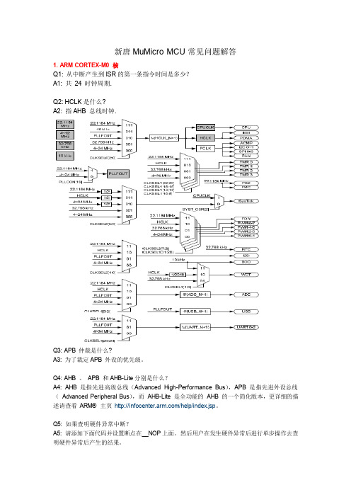
5.2 系统管理器 .................................................................................................................... 34
5.2.1 概述.................................................................................................................................34 5.2.2 系统复位..........................................................................................................................34 5.2.3 系统电源分配 ..................................................................................................................35 5.2.4 系统内存映射 ..................................................................................................................37 5.2.5 系统定时器(SysTick) .......................................................................................................39 5.2.6 嵌套向量中断控制器(NVIC).............................................................................................40
新唐Nuvoton选型指南
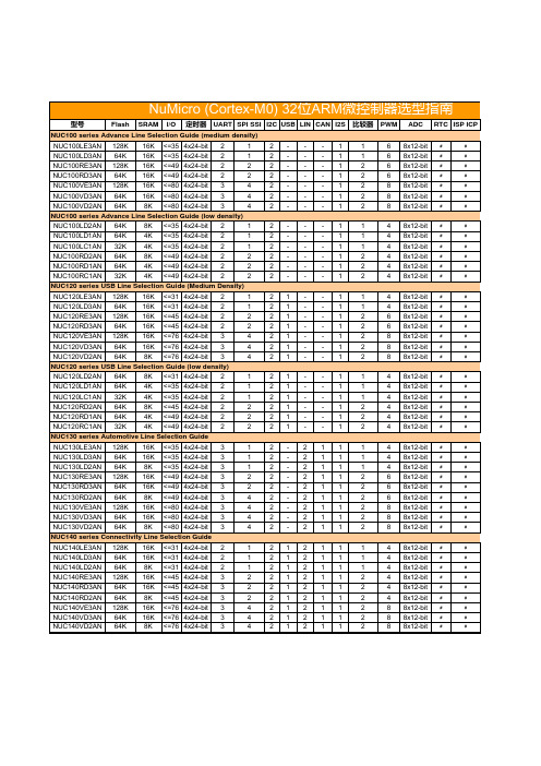
NuMicro (Cortex-M0) 32位ARM微控制器选型指南
型号 Flash SRAM I/O 定时器 UART SPI SSI I2C USB LIN CAN I2S 比较器 2 2 2 2 2 2 2 2 2 2 2 2 2 2 2 2 2 2 2 2 2 2 2 2 2 2 2 2 2 2 2 2 2 2 2 2 2 2 2 2 2 2 2 2 1 1 1 1 1 1 1 1 1 1 1 1 1 1 1 1 1 1 1 1 1 1 2 2 2 2 2 2 2 2 2 2 2 2 2 2 2 2 2 2 1 1 1 1 1 1 1 1 1 1 1 1 1 1 1 1 1 1 1 1 1 1 1 1 1 1 1 1 1 1 1 1 1 1 1 1 1 1 1 1 1 1 1 1 1 1 1 1 1 1 1 1 1 1 1 1 1 1 1 1 1 1 1 1 2 2 2 2 2 1 1 1 2 2 2 1 1 2 2 2 2 2 1 1 1 2 2 2 1 1 1 2 2 2 2 2 2 1 1 1 2 2 2 2 2 2 PWM 6 6 6 6 8 8 8 4 4 4 4 4 4 4 4 6 6 8 8 8 4 4 4 4 4 4 4 4 4 6 6 6 8 8 8 4 4 4 4 4 4 8 8 8 ADC 8x12-bit 8x12-bit 8x12-bit 8x12-bit 8x12-bit 8x12-bit 8x12-bit 8x12-bit 8x12-bit 8x12-bit 8x12-bit 8x12-bit 8x12-bit 8x12-bit 8x12-bit 8x12-bit 8x12-bit 8x12-bit 8x12-bit 8x12-bit 8x12-bit 8x12-bit 8x12-bit 8x12-bit 8x12-bit 8x12-bit 8x12-bit 8x12-bit 8x12-bit 8x12-bit 8x12-bit 8x12-bit 8x12-bit 8x12-bit 8x12-bit 8x12-bit 8x12-bit 8x12-bit 8x12-bit 8x12-bit 8x12-bit 8x12-bit 8x12-bit 8x12-bit RTC ISP ICP ﹟ ﹟ ﹟ ﹟ ﹟ ﹟ ﹟ ﹟ ﹟ ﹟ ﹟ ﹟ ﹟ ﹟ ﹟ ﹟ ﹟ ﹟ ﹟ ﹟ ﹟ ﹟ ﹟ ﹟ ﹟ ﹟ ﹟ ﹟ ﹟ ﹟ ﹟ ﹟ ﹟ ﹟ ﹟ ﹟ ﹟ ﹟ ﹟ ﹟ ﹟ ﹟ ﹟ ﹟ ﹟ ﹟ ﹟ ﹟ ﹟ ﹟ ﹟ ﹟ ﹟ ﹟ ﹟ ﹟ ﹟ ﹟ ﹟ ﹟ ﹟ ﹟ ﹟ ﹟ ﹟ ﹟ ﹟ ﹟ ﹟ ﹟ ﹟ ﹟ ﹟ ﹟ ﹟ ﹟ ﹟ ﹟ ﹟ ﹟ ﹟ ﹟ ﹟ ﹟ ﹟ ﹟ ﹟ ﹟ NUC100 series Advance Line Selection Guide (medium density) NUC100LE3AN 128K 16K <=35 4x24-bit 2 1 NUC100LD3AN 64K 16K <=35 4x24-bit 2 1 NUC100RE3AN 128K 16K <=49 4x24-bit 2 2 NUC100RD3AN 64K 16K <=49 4x24-bit 2 2 NUC100VE3AN 128K 16K <=80 4x24-bit 3 4 NUC100VD3AN 64K 16K <=80 4x24-bit 3 4 NUC100VD2AN 64K 8K <=80 4x24-bit 3 4 NUC100 series Advance Line Selection Guide (low density) NUC100LD2AN 64K 8K <=35 4x24-bit 2 1 NUC100LD1AN 64K 4K <=35 4x24-bit 2 1 NUC100LC1AN 32K 4K <=35 4x24-bit 2 1 NUC100RD2AN 64K 8K <=49 4x24-bit 2 2 NUC100RD1AN 64K 4K <=49 4x24-bit 2 2 NUC100RC1AN 32K 4K <=49 4x24-bit 2 2 NUC120 series USB Line Selection Guide (Medium Density) NUC120LE3AN 128K 16K <=31 4x24-bit 2 1 NUC120LD3AN 64K 16K <=31 4x24-bit 2 1 NUC120RE3AN 128K 16K <=45 4x24-bit 2 2 NUC120RD3AN 64K 16K <=45 4x24-bit 2 2 NUC120VE3AN 128K 16K <=76 4x24-bit 3 4 NUC120VD3AN 64K 16K <=76 4x24-bit 3 4 NUC120VD2AN 64K 8K <=76 4x24-bit 3 4 NUC120 series USB Line Selection Guide (low density) NUC120LD2AN 64K 8K <=31 4x24-bit 2 1 NUC120LD1AN 64K 4K <=35 4x24-bit 2 1 NUC120LC1AN 32K 4K <=35 4x24-bit 2 1 NUC120RD2AN 64K 8K <=45 4x24-bit 2 2 NUC120RD1AN 64K 4K <=49 4x24-bit 2 2 NUC120RC1AN 32K 4K <=49 4x24-bit 2 2 NUC130 series Automotive Line Selection Guide NUC130LE3AN 128K 16K <=35 4x24-bit NUC130LD3AN 64K 16K <=35 4x24-bit NUC130LD2AN 64K 8K <=35 4x24-bit NUC130RE3AN 128K 16K <=49 4x24-bit NUC130RD3AN 64K 16K <=49 4x24-bit NUC130RD2AN 64K 8K <=49 4x24-bit NUC130VE3AN 128K 16K <=80 4x24-bit NUC130VD3AN 64K 16K <=80 4x24-bit NUC130VD2AN 64K 8K <=80 4x24-bit NUC140 series Connectivity Line Selection Guide NUC140LE3AN NUC140LD3AN NUC140LD2AN NUC140RE3AN NUC140RD3AN NUC140RD2AN NUC140VE3AN NUC140VD3AN NUC140VD2AN 128K 64K 64K 128K 64K 64K 128K 64K 64K 16K 16K 8K 16K 16K 8K 16K 16K 8K <=31 <=31 <=31 <=45 <=45 <=45 <=76 <=76 <=76 4x24-bit 4x24-bit 4x24-bit 4x24-bit 4x24-bit 4x24-bit 4x24-bit 4x24-bit 4x24-bit 3 3 3 3 3 3 3 3 3 2 2 2 3 3 3 3 3 3 1 1 1 2 2 4 4 4 4 1 18 LQFP48 LQFP64 LQFP64 LQFP100 LQFP100 LQFP100 LQFP48 LQFP48 LQFP48 LQFP64 LQFP64 LQFP64 LQFP48 LQFP48 LQFP64 LQFP64 LQFP100 LQFP100 LQFP100 LQFP48 LQFP48 LQFP48 LQFP64 LQFP64 LQFP64 LQFP48 LQFP48 LQFP48 LQFP64 LQFP64 LQFP64 LQFP100 LQFP100 LQFP100 LQFP48 LQFP48 LQFP48 LQFP64 LQFP64 LQFP64 LQFP100 LQFP100 LQFP100 参考价
Nuvoton NuMicro ICP Programmer 用户指南(新唐MO51系列DOWNLOAD工具)
V1.17
Nuvoton NuMide
The information in this document is subject to change without notice. The Nuvoton Technology Corp. shall not be liable for technical or editorial errors or omissions contained herein; nor for incidental or consequential damages resulting from the furnishing, performance, or use of this material. This documentation may not, in whole or in part, be copied, photocopied, reproduced, translated, or reduced to any electronic medium or machine readable form without prior consent, in writing, from the Nuvoton Technology Corp. Nuvoton Technology Corp. All rights reserved.
2 Publication Release Date: Aug. 2011
Nuvoton NuMicro ICP Programmer User Guide
Table of Contents
1. 简介..........................................................
NUC100中文手册
Publication Release Date: June 20, 2011
-1-
Revision V2.02
NuMicro™ NUC100 系列规格书
3
编号信息列表及管脚名称定义 ................................................................................................... 10
3.1 NuMicro™ NUC100产品选型指南 ................................................................................. 10
5.4 通用I/O (GPIO).............................................................................................................. 46
5.4.1 概述.................................................................................................................................46
4.2 NuMicro™ NUC100 Low Density框图........................................................................... 31
桌面PC小精灵 英特尔猎豹峡谷NUC迷你主机
想要拥有一台Intel NUC小主机,这样的心心念随着第11代英特尔猎豹峡谷NUC的上市终于如愿以偿。
实际上从上一代就在关注NUC,之所以当时没有入手,主要是还没有说服自己,买一台这么小的主机究竟有什么用?以及NUC能否给出一个必须入手的理由。
2020年的9月初,英特尔正式推出搭载英特尔锐炬Xe显卡的第11代智能英特尔酷睿处理器(代号“Tiger Lake”),这次的处理器有很多新技术,比如全新Willow Cove CPU微架构,全新的SuperFin制程技术,对比上一代,运行频率显著提高。
另外一个很大的变化就是搭载的英特尔锐炬Xe显卡,不仅满足多种办公应用的需求,还能流畅运行包括《无主之地3》《孤岛惊魂:新曙光》《杀手2》和其他主流1080p游戏,相比上代产品,游戏时性能提高多至2倍。
当然,还有PCIe4.0,WiFi6(Gig+),以及雷电4等多项新特性,足够领先目前的主流配置。
此外,在桌面办公方面,相比笔记本电脑和台式机电脑的体积都要更小,意味着能够节省很多空间,连接大屏显示器也更加方便。
这款NUC是英特尔猎豹峡谷(Panther Canyon),型号为NUC11PABi7,外观规格为117mm×112mm×56mm,主机重量仅为643g,甚是轻巧,放在桌面上一点儿也不占空间,甚至可以“隐藏”起来。
前面板的左侧有一个若隐若现圆形的区域,这里是隐藏式硬盘指示灯,可以用来显示硬盘读写状态。
中间1个Thunderbolt3接口,1个USB3.1Gen2Type-A接口以及1个3.5mm耳机/麦克风插口,最右侧的电源按钮,开机后也会亮起蓝光。
主机顶部还搭载了1个无线充电区域,最高功率15W,可以为手机或耳机等小产品充电,相当方便。
需要说明的是,在另外的NUC11PAH/PAK型号上是没有无线充电功能的。
NUC主机重量为643g,就主机本身来说,倒是非常便携,但没有电源是不行的,所以在加上这个120W的适配器后,就达到了1086g,这个重量也能接受,毕竟比很多轻薄本还要轻,就是电源看上去太笨重,跟mini小主机完全不搭,希望能推出一款更小巧的适配器。
siRNA产品使用说明
siRNA产品使用说明RN:R10043.5 产品简介常规化学合成siRNA为21~25nt的双链小分子RNA,即用型。
运输保存产品以冻干粉的形式,常温运输。
收到产品后,请于-20℃~-80℃保存,冻干粉可以稳定保存一年。
使用前瞬时离心,用RNase-free HO或灭菌ddH2O,配制成20μM储存液,分装保存,避免反复冻融(不超过5次)。
2表1 20μM储存液的配置参考0.25 0.5 1 2 5 20溶解体积(μl) 12.5 25 50 100 250 1000 注:如需进行高通量筛选试验,可选择siRNA Library。
使用前须知为避免外界因素(包括酶,极端pH或者温度条件等)导致产品降解,所有操作请严格遵循RNA操作规则。
实验过程中,产品最好于冰上放置,使用完毕后请于-20℃~-80℃小心保存。
细胞实验方法:为了降低细胞密度、试剂用量,转染效率等因素导致的孔间差异,保证实验的可靠性和可重复性,一般建议:1)转染实验中每个转染样品至少设置3个复孔;2)接种细胞时,每孔接种的细胞数量尽量保持一致,且细胞在各孔的表面平均分布。
1. 转染浓度:siRNA产品最佳工作浓度因不同的细胞类型及研究目的而异。
锐博生物推荐的siRNA初始转染浓度为50nM,转染后检测时间为24~72h。
最佳转染效率一般通过设置时间曲线和浓度梯度进行优化,优化的范围建议为5~100nM。
2. 转染步骤:以ribo FECT™ CP Reagent 转染 siRNA于24孔板,转染浓度为50nM为例,其他规格容器的试剂用量请参考表2。
1)接种细胞a.贴壁细胞:以Hela细胞为例,接种1×10⁵~5×10⁵个细胞至含有适量完全培养基(v1)的24孔板培养孔中,使转染时的细胞密度能够达到30~50%。
b.悬浮细胞:以THP1细胞为例,接种1×10⁵~5×10⁵个细胞至含有适量完全培养基(v1)的24孔板培养孔中。
NUC100 Product Brief EN
ARM Cortex™-M032-BIT MICROCONTROLLER NuMicro™ FamilyNUC100 Product BriefThe information described in this document is the exclusive intellectual property ofNuvoton Technology Corporation and shall not be reproduced without permission from Nuvoton. Nuvoton is providing this document only for reference purposes of NuMicro microcontroller based system design. Nuvoton assumes no responsibility for errors or omissions.All data and specifications are subject to change without notice.For additional information or questions, please contact: Nuvoton Technology Corporation.Contents1GENERAL DESCRIPTION (6)2FEATURES (7)2.1NuMicro™ NUC100 Features – Advanced Line (7)3PARTS INFORMATION LIST AND PIN CONFIGURATION (11)3.1NuMicro™ NUC100 Products Selection Guide (11)3.1.1NuMicro™ NUC100 Medium Density Advance Line Selection Guide (11)3.1.2NuMicro™ NUC100 Low Density Advance Line Selection Guide (11)3.2Pin Configuration (13)3.2.1NuMicro™ NUC100 Medium Density Pin Diagram (13)3.2.2NuMicro™ NUC100 Low Density Pin Diagram (16)3.3Pin Description (18)3.3.1NuMicro™ NUC100 Medium Density Pin Description (18)3.3.2NuMicro™ NUC100 Low Density Pin Description (25)4BLOCK DIAGRAM (30)4.1NuMicro™ NUC100 Medium Density Block Diagram (30)4.2NuMicro™ NUC100 Low Density Block Diagram (31)5ELECTRICAL CHARACTERISTICS (31)5.1Absolute Maximum Ratings (31)5.2DC Electrical Characteristics (33)5.2.1NuMicro™ NUC100/NUC120 Medium Density DC Electrical Characteristics (33)5.2.2NuMicro™ NUC100/NUC120 Low Density DC Electrical Characteristics (38)5.2.3Operating Current Curve (Test condition: run NOP) (42)5.2.4Idle Current Curve (44)5.2.5Power Down Current Curve (46)5.3AC Electrical Characteristics (47)5.3.1External 4~24 MHz High Speed Crystal (47)5.3.2External 32.768 kHz Low Speed Crystal (48)5.3.3Internal 22.1184 MHz High Speed Oscillator (48)5.3.4Internal 10 kHz Low Speed Oscillator (48)5.4Analog Characteristics (49)5.4.1Specification of 12-bit SARADC (49)5.4.2Specification of LDO & Power management (50)5.4.3Specification of Low Voltage Reset (51)5.4.4Specification of Brown-Out Detector (51)5.4.5Specification of Power-On Reset (5 V) (51)5.4.6Specification of Temperature Sensor (52)5.4.7Specification of Comparator (52)5.4.8Specification of USB PHY (53)5.5SPI Dynamic Characteristics (54)6PACKAGE DIMENSIONS (56)6.1100L LQFP (14x14x1.4 mm footprint 2.0mm) (56)6.264L LQFP (10x10x1.4mm footprint 2.0 mm) (57)6.348L LQFP (7x7x1.4mm footprint 2.0mm) (58)7REVISION HISTORY (59)FiguresFigure 3-1 NuMicro™ NUC100 Series selection code (12)Figure 3-2 NuMicro™ NUC100 Medium Density LQFP 100-pin Pin Diagram (13)Figure 3-3 NuMicro™ NUC100 Medium Density LQFP 64-pin Pin Diagram (14)Figure 3-4 NuMicro™ NUC100 Medium Density LQFP 48-pin Pin Diagram (15)Figure 3-5 NuMicro™ NUC100 Low Density LQFP 64-pin Pin Diagram (16)Figure 3-6 NuMicro™ NUC100 Low Density LQFP 48-pin Pin Diagram (17)Figure 4-1 NuMicro™ NUC100 Medium Density Block Diagram (30)Figure 4-2 NuMicro™ NUC100 Low Density Block Diagram (31)Figure 7-1 Typical Crystal Application Circuit (47)Figure 7.5-1 SPI Master dynamic characteristics timing (55)Figure 7.5-2 SPI Slave dynamic characteristics timing (55)Table 1-1 Connectivity Supported Table (6)1 GENERAL DESCRIPTIONThe NuMicro™ NUC100 Series is 32-bit microcontrollers with embedded ARM® Cortex™-M0 core for industrial control and applications which need rich communication interfaces. The Cortex™-M0 is the newest ARM® embedded processor with 32-bit performance and at a cost equivalent to traditional 8-bit microcontroller. NuMicro™ NUC100 Series includes NUC100, NUC120, NUC130 and NUC140 product line.The NuMicro™ NUC100 Advanced Line embeds Cortex™-M0 core running up to 50 MHz with 32K/64K/128K-byte embedded flash, 4K/8K/16K-byte embedded SRAM, and 4K-byte loader ROM for the ISP. It also equips with plenty of peripheral devices, such as Timers, Watchdog Timer, RTC, PDMA, UART, SPI, I2C, I2S, PWM Timer, GPIO, PS/2, 12-bit ADC, Analog Comparator, Low Voltage Reset Controller and Brown-Out Detector.Product Line UART SPI I2C USB LIN CAN PS/2 I2S NUC100●●●●●NUC120 ●●●●●●NUC130 ●●●●●●●NUC140 ●●●●●●●●Table 1-1 Connectivity Supported Table2 FEATURESThe equipped features are dependent on the product line and their sub products.2.1 NuMicro™ NUC100 Features – Advanced Line• Core– ARM® Cortex™-M0 core runs up to 50 MHz– One 24-bit system timer– Supports low power sleep mode– Single-cycle 32-bit hardware multiplier– NVIC for the 32 interrupt inputs, each with 4-levels of priority– Serial Wire Debug supports with 2 watchpoints/4 breakpoints•Build-in LDO for wide operating voltage ranges from 2.5 V to 5.5 V• Flash Memory– 32K/64K/128K bytes Flash for program code (128KB only support in NuMicro™NUC100/NUC120 Medium Density)– 4KB flash for ISP loader– Support In-system program (ISP) application code update– 512 byte page erase for flash– Configurable data flash address and size for 128KB system, fixed 4KB data flash for the 32KB and 64KB system– Support 2 wire ICP update through SWD/ICE interface– Support fast parallel programming mode by external programmer• SRAM Memory– 4K/8K/16K bytes embedded SRAM (16KB only support in NuMicro™ NUC100/NUC120 Medium Density)– Support PDMA mode• PDMA (Peripheral DMA)– Support 9 channels PDMA for automatic data transfer between SRAM and peripherals (Only support 1 channel in NuMicro™ NUC100/NUC120 Low Density) • Clock Control– Flexible selection for different applications– Build-in 22.1184 MHz high speed oscillator (Trimmed to 1%) for system operation, and low power 10 kHz low speed oscillator for watchdog and wake-up operation – Support one PLL, up to 50 MHz, for high performance system operation– External 4~24 MHz high speed crystal input for precise timing operation– External 32.768 kHz low speed crystal input for RTC function and low power system operation• GPIO– Four I/O modes:bi-directionQuasioutputPush-PulloutputOpen-DrainInput only with high impendence– TTL/Schmitt trigger input selectable– I/O pin can be configured as interrupt source with edge/level setting– High driver and high sink IO mode support• Timer– Support 4 sets of 32-bit timers with 24-bit up-timer and one 8-bit pre-scale counter – Independent clock source for each timer– Provides one-shot, periodic, toggle and continuous counting operation modes (NuMicro™ NUC100/NUC120 Medium Density only support one-shot and periodic mode)– Support event counting function (NuMicro™ NUC100/NUC120 Low Density only)• Watchdog Timer– Multiple clock sources– 8 selectable time out period from 1.6ms ~ 26.0sec (depends on clock source)– WDT can wake-up from power down or idle mode– Interrupt or reset selectable on watchdog time-out• RTC– Support software compensation by setting frequency compensate register (FCR)– Support RTC counter (second, minute, hour) and calendar counter (day, month, year) – Support Alarm registers (second, minute, hour, day, month, year)– Selectable 12-hour or 24-hour mode– Automatic leap year recognition– Support periodic time tick interrupt with 8 period options 1/128, 1/64, 1/32, 1/16, 1/8, 1/4, 1/2 and 1 second– Support wake-up function• PWM/Capture– Built-in up to four 16-bit PWM generators provide eight PWM outputs or four complementary paired PWM outputs– Each PWM generator equipped with one clock source selector, one clock divider, one 8-bit prescaler and one Dead-Zone generator for complementary paired PWM – Up to eight 16-bit digital Capture timers (shared with PWM timers) provide eight rising/falling capture inputs– Support Capture interrupt• UART– Up to three UART controllers (NuMicro™ NUC100/NUC120 Low Density only support 2 UART controllers)– UART ports with flow control (TXD, RXD, CTS and RTS)– UART0 with 63-byte FIFO is for high speed– UART1/2(optional) with 15-byte FIFO for standard device– Support IrDA (SIR) function– Support RS-485 9-bit mode and direction control. (NuMicro™ NUC100/NUC120 Low Density Only)– Programmable baud-rate generator up to 1/16 system clock– Support PDMA mode• SPI– Up to four sets of SPI controller (NuMicro™ NUC100/NUC120 Low Density only support 2 SPI controllers)– Master up to 20 MHz, and Slave up to 10 MHz (chip working @ 5V)– Support SPI master/slave mode– Full duplex synchronous serial data transfer– Variable length of transfer data from 1 to 32 bits– MSB or LSB first data transfer– Rx and Tx on both rising or falling edge of serial clock independently– 2 slave/device select lines when it is as the master, and 1 slave/device select line when it is as the slave– Support byte suspend mode in 32-bit transmission– Support PDMA mode•I2C– Up to two sets of I2C device– Master/Slave mode– Bidirectional data transfer between masters and slaves– Multi-master bus (no central master)– Arbitration between simultaneously transmitting masters without corruption of serial data on the bus– Serial clock synchronization allows devices with different bit rates to communicate via one serial bus– Serial clock synchronization can be used as a handshake mechanism to suspend and resume serial transfer– Programmable clocks allow versatile rate control– Support multiple address recognition (four slave address with mask option)•I2S– Interface with external audio CODEC– Operate as either master or slave mode– Capable of handling 8-, 16-, 24- and 32-bit word sizes– Mono and stereo audio data supported– I2S and MSB justified data format supported– Two 8 word FIFO data buffers are provided, one for transmit and one for receive– Generates interrupt requests when buffer levels cross a programmable boundary– Support two DMA requests, one for transmit and one for receive• PS/2 Device Controller– Host communication inhibit and request to send detection– Reception frame error detection– Programmable 1 to 16 bytes transmit buffer to reduce CPU intervention– Double buffer for data reception– S/W override bus•EBI (External bus interface) support (NuMicro™ NUC100/NUC120 Low Density 64-pin Package Only)– Accessible space: 64KB in 8-bit mode or 128KB in 16-bit mode– Support 8-/16-bit data width– Support byte write in 16-bit data width mode• ADC– 12-bit SAR ADC with 600K SPS– Up to 8-ch single-end input or 4-ch differential input– Single scan/single cycle scan/continuous scan– Each channel with individual result register– Scan on enabled channels– Threshold voltage detection– Conversion start by software programming or external input– Support PDMA mode• Analog Comparator– Up to two analog comparators– External input or internal bandgap voltage selectable at negative node– Interrupt when compare result change– Power down wake-up•One built-in temperature sensor with 1℃ resolution• Brown-Out detector– With 4 levels: 4.5 V/3.8 V/2.7 V/2.2 V– Support Brown-Out Interrupt and Reset option•Low Voltage Reset– Threshold voltage levels: 2.0 V•Operating Temperature: -40℃~85℃• Packages:– All Green package (RoHS)– LQFP 100-pin / 64-pin / 48-pin (100-pin for NuMicro™ NUC100/NUC120 Medium Density Only)3 PARTS INFORMATION LIST AND PIN CONFIGURATION3.1 NuMicro ™ NUC100 Products Selection Guide3.1.1 NuMicro ™ NUC100 Medium Density Advance Line Selection GuideConnectivityPart number APROM RAMData FlashISP Loader ROMI/OTimerUART SPI I 2C USB LIN CAN I 2S Comp.PWMADCRTC EBIISPICPPackage NUC100LD3AN 64 KB 16 KB 4 KB 4 KB up to 354x32-bit 2 12- - - 1 1 6 8x12-bit v - v LQFP48NUC100LE3AN 128 KB 16 KB Definable 4 KB up to 354x32-bit 2 12- - - 1 1 6 8x12-bit v - v LQFP48NUC100RD3AN 64 KB 16 KB4 KB4 KB up to 494x32-bit 2 22- - - 1 2 6 8x12-bit v - v LQFP64NUC100RE3AN 128 KB 16 KB Definable 4 KB up to 494x32-bit 2 22- - - 1 2 6 8x12-bit v - v LQFP64NUC100VD2AN 64 KB8 KB4 KB 4 KB up to 804x32-bit 3 42- - - 1 2 8 8x12-bit v - v LQFP100NUC100VD3AN 64 KB 16 KB4 KB4 KB up to 804x32-bit 3 42- - - 1 2 8 8x12-bit v - v LQFP100NUC100VE3AN 128 KB 16 KB Definable4 KB up to 804x32-bit342---1288x12-bitv-vLQFP1003.1.2 NuMicro ™ NUC100 Low Density Advance Line Selection GuideConnectivityPart number APROM RAMData FlashISP Loader ROMI/OTimerUART SPI I 2C USB LIN CAN I 2S Comp.PWMADCRTC EBIISPICPPackage NUC100LC1BN 32 KB 4 KB 4 KB 4 KB up to 354x32-bit 2 12- - - 1 1 4 8x12-bit v - v LQFP48NUC100LD1BN 64 KB 4 KB 4 KB 4 KB up to 354x32-bit 2 12- - - 1 1 4 8x12-bit v - v LQFP48NUC100LD2BN 64 KB 8 KB 4 KB 4 KB up to 354x32-bit 2 12- - - 1 1 4 8x12-bit v - v LQFP48NUC100RC1BN 32 KB 4 KB 4 KB 4 KB up to 494x32-bit 2 22- - - 1 2 4 8x12-bit v v v LQFP64NUC100RD1BN 64 KB 4 KB 4 KB 4 KB up to 494x32-bit 2 22- - - 1 2 4 8x12-bit v v v LQFP64NUC100RD2BN 64 KB8 KB4 KB4 KB up to 494x32-bit222---1248x12-bitvvvLQFP64Figure 3-1 NuMicro™ NUC100 Series selection code3.2 Pin Configuration3.2.1 NuMicro™ NUC100 Medium Density Pin Diagram3.2.1.1 NuMicro™ NUC100 Medium Density LQFP 100 pinFigure 3-2 NuMicro™ NUC100 Medium Density LQFP 100-pin Pin Diagram3.2.1.2 NuMicro™ NUC100 Medium Density LQFP 64 pinFigure 3-3 NuMicro™ NUC100 Medium Density LQFP 64-pin Pin Diagram3.2.1.3 NuMicro ™ NUC100 Medium Density LQFP 48 pin1S C L /P A .11S D A /P A .100S C L /P A .9I 2C 0S D A /P A .8R X D 1/P B .487654Figure 3-4 NuMicro ™ NUC100 Medium Density LQFP 48-pin Pin Diagram3.2.2 NuMicro™ NUC100 Low Density Pin Diagram3.2.2.1 NuMicro™ NUC100 Low Density LQFP 64 pinNUC100LQFP 64-pinFigure 3-5 NuMicro™ NUC100 Low Density LQFP 64-pin Pin Diagram3.2.2.2 NuMicro™ NUC100 Low Density LQFP 48 pinFigure 3-6 NuMicro™ NUC100 Low Density LQFP 48-pin Pin Diagram3.3 Pin Description3.3.1 NuMicro™ NUC100 Medium Density Pin Description 3.3.1.1 NuMicro™ NUC100 Medium Density Pin DescriptionPin No.LQFP 100 LQFP64LQFP48Pin Name Pin Type Description1 PE.15 I/O General purpose input/output digital pin2 PE.14 I/O General purpose input/output digital pin3 PE.13 I/O General purpose input/output digital pinPB.14 I/O General purpose input/output digital pin/INT0 I /INT0: External interrupt1 input pin4 1SPISS31 I/O SPISS31: SPI3 2nd slave select pinPB.13 I/O General purpose input/output digital pin5 2CPO1 O Comparator1 output pinPB.12 I/O General purpose input/output digital pinCPO0 O Comparator0 output pin6 3 1CLKO O Frequency Divider output pin7 4 2X32O O External 32.768 kHz low speed crystal output pin 8 5 3X32I I External 32.768 kHz low speed crystal input pinPA.11 I/O General purpose input/output digital pin9 6 4I2C1SCL I/O I2C1SCL: I2C1 clock pinPA.10 I/O General purpose input/output digital pin10 7 5I2C1SDA I/O I2C1SDA: I2C1 data input/output pinPA.9 I/O General purpose input/output digital pin11 8 6I2C0SCL I/O I2C0SCL: I2C0 clock pinPA.8 I/O General purpose input/output digital pin12 9 7I2C0SDA I/O I2C0SDA: I2C0 data input/output pinPD.8 I/O General purpose input/output digital pin13SPISS30 I/O SPISS30: SPI3 slave select pinPD.9 I/O General purpose input/output digital pin14SPICLK3 I/O SPICLK3: SPI3 serial clock pin15 PD.10 I/O General purpose input/output digital pinPin No.LQFP 100 LQFP64LQFP48Pin Name Pin Type DescriptionMISO30 I/O MISO30: SPI3 MISO (Master In, Slave Out) pinPD.11 I/O General purpose input/output digital pin16MOSI30 I/O MOSI30: SPI3 MOSI (Master Out, Slave In) pinPD.12 I/O General purpose input/output digital pin17MISO31 I/O MISO31:SPI32nd MISO (Master In, Slave Out) pinPD.13 I/O General purpose input/output digital pin18MOSI31 I/O MOSI31:SPI32nd MOSI (Master Out, Slave In) pinPB.4 I/O General purpose input/output digital pin19 10 8RXD1 I RXD1: Data receiver input pin for UART1PB.5 I/O General purpose input/output digital pin20 11 9TXD1 O TXD1: Data transmitter output pin for UART1PB.6 I/O General purpose input/output digital pin21 12RTS1 O RTS1: Request to Send output pin for UART1PB.7 I/O General purpose input/output digital pin22 13CTS1 I CTS1: Clear to Send input pin for UART123 14 10LDO P LDO output pin24 15 11VDD P Power supply for I/O ports and LDO source for internal PLL and digital function25 16 12VSS P Ground26 PE.12 I/O General purpose input/output digital pin27 PE.11 I/O General purpose input/output digital pin28 PE.10 I/O General purpose input/output digital pin29 PE.9 I/O General purpose input/output digital pin30 PE.8 I/O General purpose input/output digital pin31 PE.7 I/O General purpose input/output digital pinPB.0 I/O General purpose input/output digital pin32 17 13RXD0 I RXD0: Data receiver input pin for UART0PB.1 I/O General purpose input/output digital pin33 18 14TXD0 O TXD0: Data transmitter output pin for UART0 34 19 15PB.2 I/O General purpose input/output digital pinPin No.LQFP 100 LQFP64LQFP48Pin Name Pin Type DescriptionRTS0 O RTS0: Request to Send output pin for UART0PB.3 I/O General purpose input/output digital pin35 20 16CTS0 I CTS0: Clear to Send input pin for UART036 21 PD.6 I/O General purpose input/output digital pin37 22 PD.7 I/O General purpose input/output digital pinPD.14 I/O General purpose input/output digital pin38 23RXD2 I RXD2: Data receiver input pin for UART2PD.15 I/O General purpose input/output digital pin39 24TXD2 O TXD2: Data transmitter output pin for UART2PC.5 I/O General purpose input/output digital pin40MOSI01 I/O MOSI01:SPI02nd MOSI (Master Out, Slave In) pinPC.4 I/O General purpose input/output digital pin41MISO01 I/O MISO01:SPI02nd MISO (Master In, Slave Out) pin PC.3 I/O General purpose input/output digital pinMOSI00 I/O MOSI00: SPI0 MOSI (Master Out, Slave In) pin 42 25 17I2SDO O I2SDO:I2S data outputPC.2 I/O General purpose input/output digital pinMISO00 I/O MISO00: SPI0 MISO (Master In, Slave Out) pin 43 26 18I2SDI I I2SDI:I2S data inputPC.1 I/O General purpose input/output digital pinSPICLK0 I/O SPICLK0: SPI0 serial clock pin44 27 19I2SBCLK I/O I2SBCLK:I2S bit clock pinPC.0 I/O General purpose input/output digital pinSPISS00 I/O SPISS00: SPI0 slave select pin45 28 20I2SLRCL K I/O I2SLRCLK:I2S left right channel clock46 PE.6 I/O General purpose input/output digital pinPE.5 I/O General purpose input/output digital pin 47 29 21PWM5 I/O PWM5: PWM output/Capture input48 30 22PB.11 I/O General purpose input/output digital pinPin No.LQFP 100 LQFP64LQFP48Pin Name Pin Type DescriptionPWM4 I/O PWM4: PWM output/Capture input31 23PB.10 I/O General purpose input/output digital pin49SPISS01I/O SPISS01: SPI0 2nd slave select pin32 24PB.9 I/O General purpose input/output digital pin50SPISS11I/O SPISS11: SPI1 2nd slave select pin51 PE.4 I/O General purpose input/output digital pin52 PE.3 I/O General purpose input/output digital pin53 PE.2 I/O General purpose input/output digital pinPE.1 I/O General purpose input/output digital pin54PWM7 I/O PWM7: PWM output/Capture inputPE.0 I/O General purpose input/output digital pin55PWM6 I/O PWM6: PWM output/Capture inputPC.13 I/O General purpose input/output digital pin56MOSI11 I/O MOSI11:SPI12nd MOSI (Master Out, Slave In) pinPC.12 I/O General purpose input/output digital pin57MISO11 I/O MISO11:SPI12nd MISO (Master In, Slave Out) pinPC.11 I/O General purpose input/output digital pin58 33MOSI10 I/O MOSI10: SPI1 MOSI (Master Out, Slave In) pinPC.10 I/O General purpose input/output digital pin59 34MISO10 I/O MISO10: SPI1 MISO (Master In, Slave Out) pinPC.9 I/O General purpose input/output digital pin60 35SPICLK1 I/O SPICLK1: SPI1 serial clock pinPC.8 I/O General purpose input/output digital pin61 36SPISS10 I/O SPISS10: SPI1 slave select pinPA.15 I/O General purpose input/output digital pinPWM3 I/O PWM3: PWM output/Capture input62 37 25I2SMCLK O I2SMCLK:I2S master clock output pinPA.14 I/O General purpose input/output digital pin63 38 26PWM2 I/O PWM2: PWM output/Capture inputPin No.LQFP 100 LQFP64LQFP48Pin Name Pin Type DescriptionPA.13 I/O General purpose input/output digital pin64 39 27PWM1 I/O PWM1: PWM output/Capture inputPA.12 I/O General purpose input/output digital pin 65 40 28PWM0 I/O PWM0: PWM output/Capture input66 41 29ICE_DAT I/O Serial Wired Debugger Data pin67 42 30ICE_CK I Serial Wired Debugger Clock pin68 VDD P Power supply for I/O ports and LDO source for internal PLL and digital circuit69 VSS P Ground70 43 31AVSS AP Ground Pin for analog circuitPA.0 I/O General purpose input/output digital pin 71 44 32ADC0 AI ADC0: ADC analog inputPA.1 I/O General purpose input/output digital pin 72 45 33ADC1 AI ADC1: ADC analog inputPA.2 I/O General purpose input/output digital pin 73 46 34ADC2 AI ADC2: ADC analog inputPA.3 I/O General purpose input/output digital pin 74 47 35ADC3 AI ADC3: ADC analog inputPA.4 I/O General purpose input/output digital pin 75 48 36ADC4 AI ADC4: ADC analog inputPA.5 I/O General purpose input/output digital pin 76 49 37ADC5 AI ADC5: ADC analog inputPA.6 I/O General purpose input/output digital pin 77 50 38ADC6 AI ADC6: ADC analog inputPA.7 I/O General purpose input/output digital pin51 39ADC7 AI ADC7: ADC analog input78SPISS21I/O SPISS21: SPI2 2nd slave select pin79 Vref AP Voltage reference input for ADC80 52 40AVDD AP Power supply for internal analog circuit 81 PD.0 I/O General purpose input/output digital pinPin No.LQFP 100 LQFP64LQFP48Pin Name Pin Type DescriptionSPISS20 I/O SPISS20: SPI2 slave select pinPD.1 I/O General purpose input/output digital pin82SPICLK2 I/O SPICLK2: SPI2 serial clock pinPD.2 I/O General purpose input/output digital pin83MISO20 I/O MISO20: SPI2 MISO (Master In, Slave Out) pinPD.3 I/O General purpose input/output digital pin84MOSI20 I/O MOSI20: SPI2 MOSI (Master Out, Slave In) pinPD.4 I/O General purpose input/output digital pin85MISO21 I/O MISO21:SPI22nd MISO (Master In, Slave Out) pinPD.5 I/O General purpose input/output digital pin86MOSI21 I/O MOSI21:SPI22nd MOSI (Master Out, Slave In) pinPC.7 I/O General purpose input/output digital pin87 53 41CPN0 AI CPN0: Comparator0 Negative input pinPC.6 I/O General purpose input/output digital pin88 54 42CPP0 AI CPP0: Comparator0 Positive input pinPC.15 I/O General purpose input/output digital pin89 55CPN1 AI CPN1: Comparator1 Negative input pinPC.14 I/O General purpose input/output digital pin90 56CPP1 AI CPP1: Comparator1 Positive input pinPB.15 I/O General purpose input/output digital pin91 57 43/INT1 I /INT1: External interrupt0 input pin92 58 44XT1_OUT O External 4~24 MHz high speed crystal output pin 93 59 45XT1_IN I External 4~24 MHz high speed crystal input pin94 60 46/RESET I External reset input: Low active, set this pin low reset chip to initial state. With internal pull-up.95 61 VSS P Ground96 62 VDD P Power supply for I/O ports and LDO source for internal PLL and digital circuit97 PS2DAT I/O PS/2 Data pin98 PS2CLK I/O PS/2 clock pin99 63 47PVSS P PLLGroundPin No.LQFP 100 LQFP64LQFP48Pin Name Pin Type DescriptionPB.8 I/O General purpose input/output digital pin100 64 48STADC I STADC: ADC external trigger input. Note: Pin Type I=Digital Input, O=Digital Output; AI=Analog Input; P=Power Pin; AP=Analog Power3.3.2 NuMicro™ NUC100 Low Density Pin Description 3.3.2.1 NuMicro™ NUC100 Low Density Pin DescriptionPin No.LQFP 64 LQFP48Pin Name Pin Type DescriptionPB.14 I/O General purpose input/output digital pin1/INT0 I /INT0: External interrupt1 input pinPB.13 I/O General purpose input/output digital pinCPO1 O Comparator1 output pin2AD1 I/O EBI Address/Data bus bit1 (64pin package only)PB.12 I/O General purpose input/output digital pinCPO0 O Comparator0 output pin1CLKO O Frequency Divider output pin3AD0 I/O EBI Address/Data bus bit0 (64pin package only) 4 2X32O O External 32.768 kHz low speed crystal output pin 5 3X32I I External 32.768 kHz low speed crystal input pinPA.11 I/O General purpose input/output digital pin 4I2C1SCL I/O I2C1SCL: I2C1 clock pin6nRD O EBI read enable output pin (64pin package only) PA.10 I/O General purpose input/output digital pin 5I2C1SDA I/O I2C1SDA: I2C1 data input/output pin7nWR O EBI write enable output pin (64pin package only) PA.9 I/O General purpose input/output digital pin8 6I2C0SCL I/O I2C0SCL: I2C0 clock pinPA.8 I/O General purpose input/output digital pin9 7I2C0SDA I/O I2C0SDA: I2C0 data input/output pinPB.4 I/O General purpose input/output digital pin10 8RXD1 I RXD1: Data receiver input pin for UART1PB.5 I/O General purpose input/output digital pin11 9TXD1 O TXD1: Data transmitter output pin for UART1PB.6 I/O General purpose input/output digital pin12RTS1 O RTS1: Request to Send output pin for UART1Pin No.LQFP 64 LQFP48Pin Name Pin Type DescriptionALE OEBI address latch enable output pin (64pinpackage only)PB.7 I/O General purpose input/output digital pinCTS1 I CTS1: Clear to Send input pin for UART113nCS O EBI chip select enable output pin (64pin package only)14 10LDO P LDO output pin15 11VDD P Power supply for I/O ports and LDO source for internal PLL and digital function16 12VSS P GroundPB.0 I/O General purpose input/output digital pin17 13RXD0 I RXD0: Data receiver input pin for UART0PB.1 I/O General purpose input/output digital pin18 14TXD0 O TXD0: Data transmitter output pin for UART0PB.2 I/O General purpose input/output digital pin15RTS0 O RTS0: Request to Send output pin for UART0 19nWRL O EBI low byte write enable output pin (64pin package only)PB.3 I/O General purpose input/output digital pin16CTS0 I CTS0: Clear to Send input pin for UART0 20nWRH O EBI high byte write enable output pin (64pin package only)21PD.6 I/O General purpose input/output digital pin22PD.7 I/O General purpose input/output digital pin23PD.14 I/O General purpose input/output digital pin24PD.15 I/O General purpose input/output digital pinPC.3 I/O General purpose input/output digital pinMOSI00 I/O MOSI00: SPI0 MOSI (Master Out, Slave In) pin 25 17I2SDO O I2SDO:I2S data outputPC.2 I/O General purpose input/output digital pinMISO00 I/O MISO00: SPI0 MISO (Master In, Slave Out) pin 26 18I2SDI I I2SDI:I2S data input。
新唐ARM Cortex -M0 NuMicro 家族选择手册
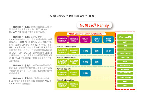
ARM Cortex™-M0 NuMicro™ 家族NuMicro™家族是新唐公司最新的,片内外设具有优异特色和连通性的,基于ARM®Cortex™-M0 的32-位微控制器产品线。
NuMicro™ 家族是基于ARM®Cortex™-M0的低功耗,高性能微控制器;它的速度达到45DMIPS 和SRAM 达到16K字节;内置Flash型EPROM 达到128K 字节,具有ISP,IAP 和ICP功能的应用使FLASH编程和升级更加快捷和灵便。
片内连通性的外设提供高速UART,SPI,I2C,I2S,CAN总线和USB 2.0全速器件接口功能。
内置混合信号单元提供8通道12-位AD转换器和2个模拟比较器并具有更高的集成度。
NuMicro™家族设计成可在宽电源电压范围内使用,更高的噪声抑制能力和工业/汽车温度等级能够满足汽车,工作控制,数据通信和消费产品的应用。
NuMicro™家族提供行业领先的与传统8-bit 微控制器成本相当的32位性能的ARM®Cortex™-M0 微控制器。
特性基于ARM® Cortex™-M0 的中央处理器内核运行速度达到50MHz一个24-位系统定时器支持低功耗睡眠模式单周期32-位硬件乘法器具有32路中断输入和每路4级优先级的NVIC SWD串行调试接口Flash 存储器SRAM GPIO、定时器、PWM、RTC 8 通道12-位ADC连通性UARTSPI/SSII2CI2SUSB 2.0CAN、LIN 总线应用领域工业控制数据通信USB 应用消费类产品马达控制汽车电子*状态:P= 量产,S=样品,UD=研发,UD (时间)= 研发(计划时间),EOL=停产。
*状态:P= 量产,S=样品,UD=研发,UD (时间)= 研发(计划时间),EOL=停产。
*状态:P= 量产,S=样品,UD=研发,UD (时间)= 研发(计划时间),EOL=停产。
NUC微控制器产品系列说明书
M251 Feature
。 Arm® Cortex®-M23 。 运行速度可达 48 MHz
M252 Feature
。 USB 2.0 全速设备无需外 挂晶振
M253 Feature
。 USB 2.0 全速设备无需外 挂晶振
。 高达五路 UART 。 CAN FD x1
2
Low Power
TrustZone
AEC-Q100
Market Trend
随着电子应用对低功耗或电池供电的需 求日益增加,现今的应用必须尽量降低 能源消耗,甚至在极端情况下,可能需 要倚赖单颗电池来维持长达 15 至 20 年 运转
低功耗应用情景包含手持式设备、居家、 AIoT、IIoT (工业物联网) 等应用情景, 使用范围十分广泛
(Programmable Serial I/O) • USB 2.0 全速装置无需外挂晶振 • 独立的 RTC 电源 VBAT 管脚
Highlight
• 支持 1.8 V ~ 5.5 V 串行接口,可连接不同电压 装置
*USCI: Universal Serial Control Interface Controller
C
1.8 3.3 5 M253
CU
3.3 5 M071
1.8 3.3 5 M252
U
3.3 5 M051
1.8 3.3 5 M251
3.3 5 Mini51
3.3 5 3.3 5
1.8 3.3 Nano100
M480 M460 M471 M453 M452 M451
E CU E CU
U C
U
Arm9™
新唐单片机最全选型表
新唐单⽚机最全选型表NuMicro? 单⽚机家族1Mini51 Base Series ⾼集成、低价位、低管脚、⾼性能32位微控制器Contact us: NuMicro@/doc/84abc79a6edb6f1afe001f27.htmlNuMicro? 单⽚机家族Mini51 系列NuMicro ? 是新唐科技新⼀代32位微控制器,采⽤ARM 公司低功耗、具精简指令代码特性的Cortex ?-M0与Cortex ?-M4处理器为核⼼,适合⼴泛的微控制器应⽤领域。
NuMicro ? Cortex ?-M0家族⽬前已量产系列有:NUC100系列与NUC200系列;带有USB 2.0全速设备的低功耗NUC120/NUC122/NUC123系列与NUC220系列;内嵌最多2組CAN 总线NUC130/131/140与NUC230/240系列;⾼性价⽐的M051/M0518系列;低管脚、低价位的Mini51系列;超低功耗运⾏的Nano100/102/112系列,0.65uA (待機功耗,内存数据保存),内嵌LCD 驱动 Nano110/112 系列, USB 2.0全速设备的超低功耗Nano120系列;⾼整合度 LCD 驱动与USB 2.0全速设备的超低功耗 Nano130系列。
Cortex ?-M4家族之⾼性能NUC442/472系列,其包含丰富外设,如以太⽹、USB OTG 和⾼速设备、双CAN 总线等等;具⾼整合度的M451系列,其带有USB OTG 和全速设备,CAN 总线,可调电压接⼝(VAI),⾼分辨率PWM 。
NuMicro ?家族的Cortex ?-M0与Cortex ?-M4微处理器为各种应⽤提供了32位最佳的性价⽐选择。
NuMicro ? Mini51系列为32位单⽚机,内建ARM ? Cortex ?-M0 内核最⾼可运⾏⾄24MHz ,具4K/8K/16K 字节Flash 内存、2K 字节内建SRAM 、可配置的数据Flash(与程序Flash 内存共享)、2K 独⽴Flash 字节作为在线系统编程(In System Programming)⽤途。
siRNA产品使用说明
siRNA产品使用说明RN:R10043.5 产品简介常规化学合成siRNA为21~25nt的双链小分子RNA,即用型。
运输保存产品以冻干粉的形式,常温运输。
收到产品后,请于-20℃~-80℃保存,冻干粉可以稳定保存一年。
使用前瞬时离心,用RNase-free HO或灭菌ddH2O,配制成20μM储存液,分装保存,避免反复冻融(不超过5次)。
2表1 20μM储存液的配置参考0.25 0.5 1 2 5 20溶解体积(μl) 12.5 25 50 100 250 1000 注:如需进行高通量筛选试验,可选择siRNA Library。
使用前须知为避免外界因素(包括酶,极端pH或者温度条件等)导致产品降解,所有操作请严格遵循RNA操作规则。
实验过程中,产品最好于冰上放置,使用完毕后请于-20℃~-80℃小心保存。
细胞实验方法:为了降低细胞密度、试剂用量,转染效率等因素导致的孔间差异,保证实验的可靠性和可重复性,一般建议:1)转染实验中每个转染样品至少设置3个复孔;2)接种细胞时,每孔接种的细胞数量尽量保持一致,且细胞在各孔的表面平均分布。
1. 转染浓度:siRNA产品最佳工作浓度因不同的细胞类型及研究目的而异。
锐博生物推荐的siRNA初始转染浓度为50nM,转染后检测时间为24~72h。
最佳转染效率一般通过设置时间曲线和浓度梯度进行优化,优化的范围建议为5~100nM。
2. 转染步骤:以ribo FECT™ CP Reagent 转染 siRNA于24孔板,转染浓度为50nM为例,其他规格容器的试剂用量请参考表2。
1)接种细胞a.贴壁细胞:以Hela细胞为例,接种1×10⁵~5×10⁵个细胞至含有适量完全培养基(v1)的24孔板培养孔中,使转染时的细胞密度能够达到30~50%。
b.悬浮细胞:以THP1细胞为例,接种1×10⁵~5×10⁵个细胞至含有适量完全培养基(v1)的24孔板培养孔中。
新唐MuMicro常见问题解答
新唐MuMicro MCU常见问题解答1. ARM CORTEX-M0 核Q1: 从中断产生到ISR的第一条指令时间是多少?A1: 共24 时钟周期.Q2: HCLK是什么?A2: 指AHB 总线时钟.Q3: APB 仲裁是什么?A3: 为了裁定APB 外设的优先级。
Q4: AHB 、APB 和AHB-Lite分别是什么?A4: AHB 是指先进高级总线(Advanced High-Performance Bus),APB 是指先进外设总线(Advanced Peripheral Bus),而AHB-Lite 是全功能的AHB 的一个简化版本,更详细的描述请查看ARM®主页/help/index.jsp。
Q5: 如果查明硬件异常中断?A5: 请添加下面代码并设置断点在__NOP上面。
然后用户在发生硬件异常后进行单步操作去查明硬件异常后产生的结果。
Q6: Cortex™-M0A6: 请查阅ARM®主页的Cortex™ -M0 技术参考文档,连接为:/help/index.jsp。
Q7: 是否存在器件唯一ID(CPUID)? 如果用户加密芯片需要用到器件唯一ID?A7: 存在。
UID (Unique ID):新唐将以上所述系列芯片植入UID,每一芯片UID是独特唯一的,使用者可利用此唯一码在韧体程序中对欲操作芯片加入判断机制,如此便可避免他人窃取程序代码重现相同商品可能。
不支持UID 的晶片如下,NUC100xxAN 系列,NUC100xxBN 系列,M05xxAN 系列,NUC102xx系列支持UID的晶片如下,Q8: NVIC是什么? 它支持多少级优先级?A8: NVIC 嵌套中断向量控制器,它支持4级优先级。
2. 系统管理Q1: NUC100 家族可以用IO口支持外部SRAM吗??A1: 有部分支持,请查看NuMicro™家族的选型手册器件是否支持外部总线接口(EBI),選型手册連結如下:/hq/enu/ProductAndSales/ProductLines/IndustrialIC/ARMMicrocontrol ler/ARMCortexTMM0/Pages/M0ProdSelectionEx.aspxQ2: 如何进入睡眠(待机模式) 和深度睡眠 (下电模式)?A2: 请查看如下的指令进入睡眠模式和下电模式:待机模式下电模式UNLOCKREG();SCB->SCR = 4;SYSCLK->PWRCON.WINT_EN = 0; SYSCLK->PWRCON.PD_WAIT_CPU = 1;SYSCLK->PWRCON.PWR_DOWN = 0;LOCKREG();__WFI(); UNLOCKREG();SCB->SCR = 4;SYSCLK->PWRCON.WINT_EN = 0; SYSCLK->PWRCON.PD_WAIT_CPU = 1;SYSCLK->PWRCON.PWR_DOWN = 1;LOCKREG();__WFI();在待机模式模式下仅CPU时钟是禁能的。
04_NuMicro家族介绍

Power 管理
Normal Run Mode
弹性CPU系统时钟源选择 所有外围设备的时钟可以单独开/关.
Sleep Mode (IDLE Mode)
CPU 停止运行, 外围设备可能还在run,这依靠应 用程序的设定
Deep Sleep Mode (Power Down Mode)
CPU &大多外围设备都停止运行
NUC100 Advance Line
Up Up to to 128KB 128KB Flash Flash ROM ROM Up Up to to 16KB 16KB SRAM SRAM
M051 Base Line
Up Up to to 64KB 64KB Flash Flash ROM ROM Up Up to to 4KB 4KB SRAM SRAM
UART UART SPI SPI
NUC140 Connectivity Line
Up Up to to 128KB 128KB Flash Flash ROM ROM Up Up to to 16KB 16KB SRAM SRAM CAN CAN LIN LIN USB USB
2 II2 C C 2 II2 S S
Vector table 基地址固定在 0x00000000
0x0
Word 0 Word 1 Word 2
Initial value of stack Vector address of exception 1 Vector address of excepaddress of exception n
interrupt 0 : Interrupt 31
Interrupt number
NVIC
英特尔100系列型号全解
信息大爆炸时代科技发展之迅速,电子通讯产业只有不短突破瓶颈才能立于不败之地,英特尔网卡线下从百兆、千兆、万兆再到25G网卡、40G网卡,一路的发展是英特尔实力的见证,如今英特尔网卡100系列的推出更显示出英特尔在网络互联技术中走在了最前端,那么它的型号又是如何分类的呢?英特尔100系列分别有两个网卡型号:英特尔58G网卡100HFA018:适应插槽:PCI-E X8传输速率: 58Gbps英特尔100G网卡100HFA016: 适应插槽:PCI-E X16传输速率: 100Gbps此两款英特尔网卡100系列都为单口网卡通常用于高端网络设备、服务器、计算机网络领域,兼容单模多模模块。
100系列网卡采用专用的高性能计算(HPC)设计和可扩展的系统框架,因此支持复杂的应用程序,有效平衡工作负载。
高级服务性质量(QoS)其为主机结构接口提供了强大而有效的传输管制。
其数据被分段为65位流控制数字(FLIT),它们组装成更大的链接,传输数据包(LTP)用于高效线路转让。
通过管理FLIT 的流量等级,此系列网卡全方位架构边缘和导向开关能够制作极其细腻的换决策以优化延迟,吞吐量和弹性更多有效适用于所有流量类型。
采用HPC 材质的优点1.可支持端到端的优化2. 可扩展,低延迟的MPI3.高MPI 消息率(160mmps )4.高效的存储与新的8K 通信和10K MTU5.网络延迟控制和QoS (具有确定性延迟)功耗低可扩展主要特征100 Gbps 链路速度x16版本(支持完整版数据速率)x8版(PCIe 限定版)MSI-X 中断处理为高多核主机上的性能高可靠性和弹性100系列网卡凭借其有载设计,消除了固件和外部存储器对数据路径的需求,而主机内存中的信息保持所有连接状态,ECC 保护提供停机时间防止错误故障, 这可减少数据错误的可能性。
HFI 规格总线接口PCI Express * Gen3 x16或PCI Express *Gen3 x8设备类型• End point (端点)高级中断图为Intel 58G 网卡100HFA018•MSI-X•INTxHFI规范和接口ASIC•单个英特尔OP HFI ASIC高数据速率•100 Gbps - PCIe x16•56 Gbps - PCIe x8(有效率为图为Intel 100G网卡100HFA01656Gbps由PCIe x8接口决定;英特尔100系列的运行速度最高可达100Gbps)虚拟通道•可配置一到八个VL加一个管理VLMTU•可配置的MTU大小为2 KB,4 KB,8 KB或10KB接口•支持QSFP28四核小型可插拔光学收发器和有源光学器件电缆华天易达专注intel网卡代理,不断完善产品链与产品更新,不断升级售后服务保障系统,为客户提供更加满意的服务。
nuvoton NUC1XX 系列 前期规格书
目录1概述 (7)2特性 (8)2.1NUC101 特征 (8)2.2NUC100 特征 (12)2.3NUC120 特征 (15)2.4NUC130 特征 (19)2.5NUC140 特征 (23)3编号信息列表及管脚名称定义 (27)3.1产品选型指南 (27)3.1.1NUC101 产品选型指南 (27)3.1.2NUC100产品选型指南 (28)3.1.3NUC120产品选型指南 (29)3.1.4NUC130产品选型指南 (30)3.1.5NUC140产品选型指南 (31)3.2管脚配置 (32)3.2.1NUC101 LQFP 100 pin (32)3.2.2NUC101 LQFP 64 pin (33)3.2.3NUC101 LQFP 48 pin (34)3.2.4NUC100 LQFP 100 pin (35)3.2.5NUC100 LQFP 64 pin (36)3.2.6NUC100 LQFP 48 pin (37)3.2.7NUC120 LQFP 100 pin (38)3.2.8NUC120 LQFP 64 pin (39)3.2.9NUC120 LQFP 48 pin (40)3.2.10NUC130 LQFP 100 pin (41)3.2.11NUC130 LQFP 64 pin (42)3.2.12NUC130 LQFP 48 pin (43)3.2.13NUC140 LQFP 100 pin (44)3.2.14NUC140 LQFP 64 pin (45)3.2.15NUC140 LQFP 48 pin (46)3.3管脚功能描述 (47)3.3.1NUC101管脚定义 (47)3.3.2NUC100 管脚定义 (54)3.3.3NUC120 Pin Description (61)3.3.4NUC130 管脚定义 (68)3.3.5NUC140 管脚定义 (76)4框图 (83)4.1NUC101 框图 (83)4.2NUC100 框图 (84)4.3NUC120 框图 (85)4.4NUC130框图 (86)4.5NUC140框图 (87)5功能描述 (88)5.1ARM® Cortex™-M0 内核 (88)5.2系统管理器 (90)5.2.1概述 (90)5.2.2系统复位 (90)5.2.3系统内存 (91)5.2.4系统管理器控制寄存器 (93)5.2.5系统定时器 (SysTick) (122)5.2.6嵌套向量中断控制器 (NVIC) (125)5.2.7系统控制寄存器 (151)5.3时钟控制器 (157)5.3.1时钟发生器 (157)5.3.2系统时钟 & SysTick 时钟 (158)5.3.3外围设备时钟 (159)5.3.4掉电模式(深度休眠模式) 时钟 (159)5.3.5分频器输出 (160)5.3.6时钟控制寄存器列表 (161)5.3.7时钟控制寄存器描述 (162)5.4USB 设备控制器 (181)5.4.1概述 (181)5.4.2特征 (181)5.4.3框图 (182)5.4.4功能描述 (183)5.4.5与USB外设通信处理 (184)5.4.6内存图 (185)5.4.7USB控制寄存器描述 (187)5.5通用 I/O (201)5.5.1概述与特征 (201)5.5.2GPIO控制寄存器图 (203)5.5.3GPIO控制寄存器描述 (205)5.6I2C 总线控制器 (主机/从机) (216)5.6.1简介 (216)5.6.2I2C 寄存器 (220)5.6.3寄存器说明 (224)5.6.4寄存器描述 (225)5.6.5I2C 操作模式 (233)5.6.6数据传输5种操作 (234)5.7PWM 发生器和捕捉定时器 (240)5.7.1简介 (240)5.7.2特性 (241)5.7.3PWM发生器结构 (242)5.7.4PWM定时器操作 (246)5.7.5PWM 双缓存,自动重载以及单触发模式 (247)5.7.6可调占空比 (248)5.7.7死区发生器 (249)5.7.8捕捉模式 (250)5.7.9PWM定时器中断结构 (251)5.7.10PWM定时器开启步骤 (252)5.7.11PWM定时器关闭步骤 (253)5.7.12捕捉开始步骤 (254)5.7.13寄存器列表 (255)5.7.14寄存器描述 (259)5.8实时时钟(RTC) (295)5.8.1概述 (295)5.8.2RTC 特征 (295)5.8.3RTC模块框图 (296)5.8.4RTC功能描述 (297)5.8.5寄存器列表 (299)5.8.6寄存器描述 (300)5.9串行外围设备接口(SPI)控制器 (315)5.9.1概述 (315)5.9.2特性 (315)5.9.3SPI模块方块图 (主机/从机) (316)5.9.4SPI时序波形图(主机/从机) (317)5.9.5SPI 编程例程 (319)5.9.6改变时钟频率 (321)5.9.7SPI 串行总线控制寄存器列表 (322)5.9.8SPI (MICROWIRE) 控制寄存器描述 (323)5.10定时器控制器 (333)5.10.1通用定时器控制器 (333)5.10.2特征 (333)5.10.3定时器控制器框图 (334)5.10.4定时器控制器寄存器图 (335)5.11看门狗定时器 (341)5.11.1看门狗定时器控制寄存器图 (343)5.12UART 接口控制器 (346)5.12.1概述 (346)5.12.2UART控制器特性 (348)5.12.3框图 (349)5.12.4IrDA 模式 (351)5.12.5LIN (Local Interconnection Network) 模式 (353)5.12.6UART接口控制寄存器列表 (354)5.12.7UART 接口控制寄存器描述 (356)5.13局域控制网络总线(CAN Bus) (381)5.13.1简介 (381)5.13.2特性 (381)5.13.3框图 (382)5.13.4功能描述 (383)5.13.5控制寄存器列表 (390)5.14PS2设备控制器(PS2D) (417)5.14.1概述 (417)5.14.2特性 (417)5.14.3PS/2 系统框图 (418)5.14.4PS/2 通讯 (419)5.14.5TX FIFO 运作 (422)5.14.6PS2 设备控制寄存器图表 (423)5.14.7寄存器描述 (424)5.15I2S 控制器 (431)5.15.1概述 (431)5.15.2特征 (431)5.15.3I2S 框图 (432)5.15.4I2S 操作 (433)5.15.5FIFO 操作 (434)5.15.6I2S 控制寄存器表 (435)5.15.7I2S 控制寄存器描述 (436)5.16模拟数字转换(ADC) (449)5.16.1功能概述 (449)5.16.2特征 (449)5.16.3框图 (450)5.16.4操作步骤 (452)5.16.5ADC寄存器列表 (459)5.16.6ADC寄存器描述 (460)5.17模拟比较器 (471)5.17.1功能描述 (471)5.17.2特征 (471)5.17.3框图 (471)5.17.4操作步骤 (472)5.17.5寄存器列表 (473)5.17.6寄存器描述 (474)5.18PDMA 控制器 (478)5.18.1概述 (478)5.18.2特性 (478)5.18.3框图 (479)5.18.4功能描述 (480)5.18.5PDMA 控制器寄存器列表 (481)5.18.6PDMA 控制寄存器描述 (482)6FLASH 内存控制器 (FMC) (505)6.1概述 (505)6.2特征 (505)6.3Flash 内存控制器框图 (506)6.4Flash 内存结构 (507)6.5启动选择 (509)6.6数据 Flash (509)6.7用户配置 (510)6.8在系统编程(ISP) (513)6.8.1ISP 程序 (513)6.9Flash控制寄存器图 (516)6.10Flash 控制寄存器描述 (517)7电气特性 (527)7.1绝对最大额定值 (527)7.2DC 电气特性 (528)7.3AC电气特性 (530)7.3.1外部晶振 XTAL1 (530)7.3.2外部32KHz晶振 XTAL (532)7.3.3内部22.1184MHz RC晶振 (532)7.3.4内部10KHz RC 晶振 (532)7.4模拟量特性 (533)7.4.11-MS/s 12-位 SARADC特性 (533)7.4.2LDO规格 & Power 管理 (534)7.4.3低压复位说明 (535)7.4.4欠压检测说明 (535)7.4.5上电复位说明(5V) (535)7.4.6温度传感器说明 (536)7.4.7比较器说明 (536)7.4.8USB PHY说明 (537)8封装定义 (539)8.1.1100L LQFP (14x14x1.4 mm footprint 2.0mm) (539)8.1.264L LQFP (10x10x1.4mm footprint 2.0 mm ) (540)8.1.348L LQFP (7x7x1.4mm footprint 2.0mm) (541)9版本信息 (542)1 概述The NUC1xx系列是32位的内嵌ARM® Cortex™-M0核的微控制器 ,适用于工业控制和需要丰富的通信接口的应用领域,Cortex™-M0是ARM最新的 32位嵌入式处理器,拥有与传统8051单片机之匹敌的价格优势. NUC1xx 系列包括 NUC100, NUC101, NUC120, NUC130 与NUC140.NUC100 Cortex™-M0内核系列最高可运行至50MHz外部时钟,内建32K/64K/128K字节内建Flash存储器,4K/8K/16K字节内建SRAM。
云端中国芯
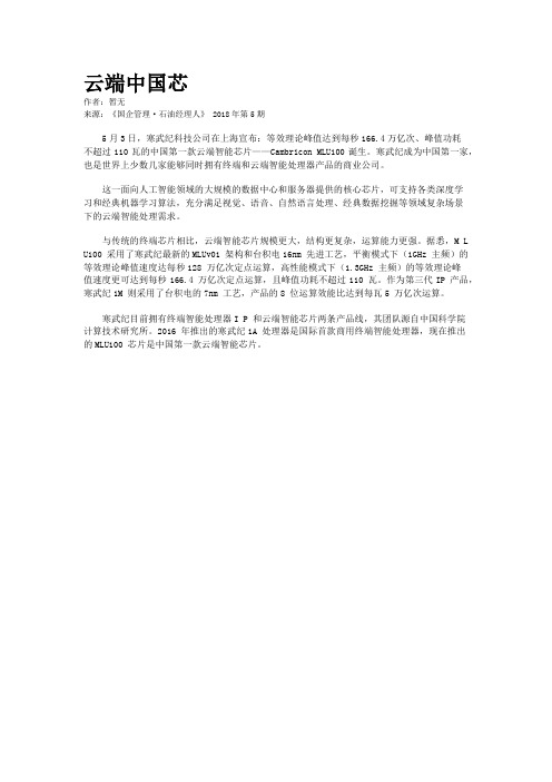
云端中国芯
作者:暂无
来源:《国企管理·石油经理人》 2018年第5期
5月3日,寒武纪科技公司在上海宣布:等效理论峰值达到每秒166.4万亿次、峰值功耗
不超过110瓦的中国第一款云端智能芯片——Cambricon MLU100诞生。
寒武纪成为中国第一家,也是世界上少数几家能够同时拥有终端和云端智能处理器产品的商业公司。
这一面向人工智能领域的大规模的数据中心和服务器提供的核心芯片,可支持各类深度学
习和经典机器学习算法,充分满足视觉、语音、自然语言处理、经典数据挖掘等领域复杂场景
下的云端智能处理需求。
与传统的终端芯片相比,云端智能芯片规模更大,结构更复杂,运算能力更强。
据悉,M L U100 采用了寒武纪最新的MLUv01 架构和台积电16nm 先进工艺,平衡模式下(1GHz 主频)的等效理论峰值速度达每秒128 万亿次定点运算,高性能模式下(1.3GHz 主频)的等效理论峰
值速度更可达到每秒166.4 万亿次定点运算,且峰值功耗不超过110 瓦。
作为第三代IP 产品,寒武纪1M 则采用了台积电的7nm 工艺,产品的8 位运算效能比达到每瓦5 万亿次运算。
寒武纪目前拥有终端智能处理器I P 和云端智能芯片两条产品线,其团队源自中国科学院
计算技术研究所。
2016 年推出的寒武纪1A 处理器是国际首款商用终端智能处理器,现在推出
的MLU100 芯片是中国第一款云端智能芯片。
NUC的黑苹果迷你PC,一不小心成为客厅100寸激光电视的灵魂!
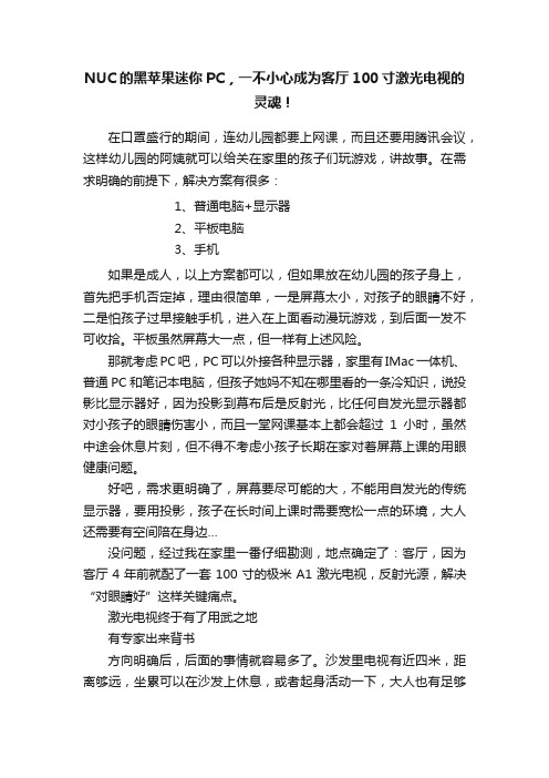
NUC的黑苹果迷你PC,一不小心成为客厅100寸激光电视的灵魂!在口罩盛行的期间,连幼儿园都要上网课,而且还要用腾讯会议,这样幼儿园的阿姨就可以给关在家里的孩子们玩游戏,讲故事。
在需求明确的前提下,解决方案有很多:1、普通电脑+显示器2、平板电脑3、手机如果是成人,以上方案都可以,但如果放在幼儿园的孩子身上,首先把手机否定掉,理由很简单,一是屏幕太小,对孩子的眼睛不好,二是怕孩子过早接触手机,进入在上面看动漫玩游戏,到后面一发不可收拾。
平板虽然屏幕大一点,但一样有上述风险。
那就考虑PC吧,PC可以外接各种显示器,家里有IMac一体机、普通PC和笔记本电脑,但孩子她妈不知在哪里看的一条冷知识,说投影比显示器好,因为投影到幕布后是反射光,比任何自发光显示器都对小孩子的眼睛伤害小,而且一堂网课基本上都会超过1小时,虽然中途会休息片刻,但不得不考虑小孩子长期在家对着屏幕上课的用眼健康问题。
好吧,需求更明确了,屏幕要尽可能的大,不能用自发光的传统显示器,要用投影,孩子在长时间上课时需要宽松一点的环境,大人还需要有空间陪在身边…没问题,经过我在家里一番仔细勘测,地点确定了:客厅,因为客厅4年前就配了一套100寸的极米A1激光电视,反射光源,解决“对眼睛好”这样关键痛点。
激光电视终于有了用武之地有专家出来背书方向明确后,后面的事情就容易多了。
沙发里电视有近四米,距离够远,坐累可以在沙发上休息,或者起身活动一下,大人也有足够的安全陪伴在身边。
接下来顺理成章就要考虑PC的事情。
既然是外接激光电视,首先排除IMac一体机,虽然可以用雷电接口上激光电视,但自己硕大的屏幕在那里啥用没有;其次排除台式PC,因为体积够大(E5神教U,X99大板,机箱也够大)放在客厅那个位置都显得突兀,显得十分不和谐;最后排除笔记本,孩子小,不仅对啥都好奇,还喜欢动手动脚,想想她噼里啪啦敲着笔记本键盘,再无意识地往桌边一推…哐当!)否定书房的大PC这样就有点麻烦了,用什么来做上网课的电脑呢?主机要足够小,最好小到可以在客厅不显山不露水地藏起来,这样既不占地又安全。
- 1、下载文档前请自行甄别文档内容的完整性,平台不提供额外的编辑、内容补充、找答案等附加服务。
- 2、"仅部分预览"的文档,不可在线预览部分如存在完整性等问题,可反馈申请退款(可完整预览的文档不适用该条件!)。
- 3、如文档侵犯您的权益,请联系客服反馈,我们会尽快为您处理(人工客服工作时间:9:00-18:30)。
3.3.2 NuMicro™ NUC100 Low Density引脚定义 ......................................................................23
4
电气特性 .................................................................................................................................... 29
2
特性 ............................................................................................................................................. 5
2.1 NuMicro™ NUC100 特征 – Advanced Line..................................................................... 5
Nuvoton is providing this document only for reference purposes of NuMicro microcontroller based system design. Nuvoton assumes no responsibility for errors or omissions. All data and specifications are subject to change without notice.
4.4 模拟量特性 .................................................................................................................... 47
4.4.1 12位SARADC特性 ..........................................................................................................47 4.4.2 LDO规格 & Power 管理...................................................................................................48 4.4.3 低压复位说明 ..................................................................................................................49 4.4.4 欠压检测说明 ..................................................................................................................49 4.4.5 上电复位说明(5V)............................................................................................................49 4.4.6 温度传感器说明 ...............................................................................................................50 4.4.7 比较器说明 ......................................................................................................................50 4.4.8 USB PHY说明 .................................................................................................................51
4.5 SPI 动态特性................................................................................................................. 52
4.2.1 NuMicro™ NUC100/NUC120 Medium Density DC电气特性 ...........................................30 4.2.2 NuMicro™ NUC100/NUC120 Low Density系列DC电气特性 ...........................................35 4.2.3 工作电流曲线(测试条件: run NOP) ..................................................................................39 4.2.4 Idle电流曲线 ....................................................................................................................42 4.2.5 Power Down电流曲线 .....................................................................................................44
目录-
1
概述 ............................................................................................................................................. 4
4.1 绝对最大额定值............................................................................................................. 29
4.2 DC电气特性 .................................................................................................................. 30
3.2 管脚配置........................................................................................................................ 11
3.2.1 NuMicro™ NUC100 Medium Density 管脚图...................................................................11 3.2.2 NuMicro™ NUC100 Low Density管脚图 ..........................................................................14
3.1.1 NuMicro™ NUC100 Medium Density Advance Line 选型指南...........................................9 3.1.2 NuMicro™ NUC100 Low Density Advance Line选型指南..................................................9
3.3 管脚功能描述 ................................................................................................................ 16
3.3.1 NuMicro™ NUC100 Medium Density管脚定义 ................................................................16
4.3 AC 电气特性.................................................................................................................. 45
4.3.1 外部 4~24 MHz 高速晶振 ................................................................................................45 4.3.2 外部 32.768 KHz 低速晶振..............................................................................................46 4.3.3 内部 22.1184 MHz 高速振荡器........................................................................................46 4.3.4 内部 10 KHz 低速振荡器 .................................................................................................46