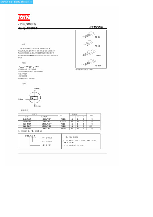
STP3NC60中文资料
三极管参数中文与英文对照(精)

三极管参数中文与英文对照(精)电阻模型参数R 电阻倍率因子TC1 线性温度系数TC2 二次温度系数电容模型参数C 电容倍率因子VC1 线性电压系数VC2 二次电压系数TC1 线性温度系数TC2 二次温度系数电感模型参数L 电感倍率因子IL1 线性电流系数IL2 二次电流系数TC1 线性温度系数TC2 二次温度系数二极管模型参数IS 饱和电流RS 寄生串联电阻N 发射系数TT 渡越时间CJO 零偏压 PN 结电容VJ PN 结自建电势M PN 结剃度因子EG 禁带宽度XT1 IS 的温度指数FC 正偏耗尽层电容系数BV 反向击穿电压(漆点电压 IBV 反向击穿电流(漆点电流 KF 闪烁躁声系数AF 闪烁躁声指数双极晶体管(三极管IS 传输饱和电流EG 禁带宽度XTI (PT IS 的温度效应指数 BF 正向电流放大系数NF 正向电流发射系数V AF (V A 正向欧拉电压IKF (IK 正向漆点电流ISE (C2 B-E 漏饱和电流NE B-E 漏饱和电流BR 反向电流放大系数NR 反向电流发射系数V AR (VB 正想欧拉电压IKR 反向漆点电流ISC C4 B-C 漏饱和电流NC B-C 漏发射系数RB 零偏压基极电阻IRB 基极电阻降致 RBM/2时的电流RE 发射区串联电阻RC 集电极电阻CJE 零偏发射结 PN 结电容VJE PE 发射结内建电势MJE ME 集电结剃度因子CJC 零偏衬底结 PN 结电容VJC PC 集电结内建电势MJC MC 集电结剃度因子XCJC Cbe 接至内部 Rb 的内部CJS CCS 零偏衬底结 PN 结电容VJS PS 衬底结构 PN 结电容MJS MS 衬底结剃度因子FC 正偏势垒电容系数TF 正向渡越时间XTF TF 随偏置变化的系数VTF TF 随 VBC 变化的电压参数ITF 影响 TF 的大电流参数PTF 在 F=1/(2派 TF Hz 时超前相移 TR 反向渡越时间XTB BF 和 BR 的温度系数KF I/F躁声系数AF I/F躁声指数Is=14.34f 反向饱和电流。
IXFN36N60中文资料
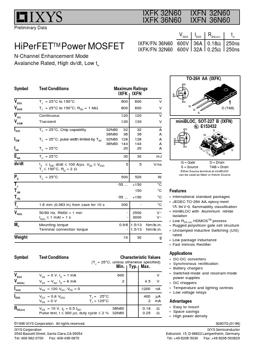
V DSSI D25R DS(on)t rr IXFK/FN 36N60600V 36A 0.18Ω250ns IXFK/FN 32N60600V 32A0.25Ω250nsPreliminary DataSymbol Test Conditions Maximum Ratings IXFK IXFNV DSS T J = 25°C to 150°C600600V V DGR T J = 25° C to 150°C; R GS = 1 M Ω600600V V GS Continuous ±20±20V V GSM Transient±30±30V I D25T C = 25°C, Chip capability 32N603232A 36N603636A I DM T C = 25°C, pulse width limited by T JM 32N60128128A 36N60144144A I AR T C = 25°C 2020A E AR T C = 25°C3030mJ dv/dt I S ≤ I DM , di/dt ≤ 100 A/µs, V DD ≤ V DSS 55V/ns T J ≤ 150°C, R G = 2 ΩP D T C = 25°C500520W T J -55 ... +150°C T JM 150°C T stg -55 ... +150°C T L 1.6 mm (0.063 in) from case for 10 s 300-°C V ISOL 50/60 Hz, RMSt = 1 min -2500V~I ISOL ≤ 1 mAt = 1 s-3000V~M d Mounting torque 0.9/6 1.5/13Nm/lb.in.Terminal connection torque - 1.5/13Nm/lb.in.Weight1030gFeatures•International standard packages •JEDEC TO-264 AA, epoxy meetUL 94 V-0, flammability classification •miniBLOC with Aluminium nitride isolation•Low R DS (on) HDMOS TM process•Rugged polysilicon gate cell structure •Unclamped Inductive Switching (UIS)rated•Low package inductance •Fast intrinsic RectifierApplications•DC-DC converters•Synchronous rectification •Battery chargers•Switched-mode and resonant-mode power supplies •DC choppers•Temperature and lighting controls •Low voltage relays Advantages •Easy to mount •Space savings•High power densityHiPerFET TMPower MOSFETN-Channel Enhancement ModeAvalanche Rated, High dv/dt, Low t rrSymbol Test ConditionsCharacteristic Values(T J = 25°C, unless otherwise specified)Min.Typ.Max.V DSS V GS = 0 V, I D = 1 mA 600V V GH(th)V DS = V GS , I D = 8 mA 24.5V I GSS V GS = ±20 V DC , V DS = 0±200nA I DSS V DS = 0.8 V DSS T J = 25°C 400µA V GS = 0 VT J = 125°C2mA R DS(on)V GS = 10 V, I D = 0.5 I D2536N600.18ΩPulse test, t ≤ 300 µs, duty cycle ≤ 2 %32N600.25ΩTO-264 AA (IXFK)SG D D (TAB)SminiBLOC, SOT-227 B (IXFN)E153432S GDMillimeter InchesMin.Max.Min.Max.A 4.82 5.13.190.202A1 2.54 2.89.100.114A2 2.00 2.10.079.083b 1.12 1.42.044.056b1 2.39 2.69.094.106b2 2.90 3.09.114.122c 0.530.83.021.033D 25.9126.16 1.020 1.030E 19.8119.96.780.786e 5.46 BSC .215 BSC J 0.000.25.000.010K 0.000.25.000.010L 20.3220.83.800.820L1 2.29 2.59.090.102P 3.17 3.66.125.144Q 6.07 6.27.239.247Q18.388.69.330.342R 3.81 4.32.150.170R1 1.78 2.29.070.090S 6.04 6.30.238.248T1.57 1.83.062.072Dim.miniBLOC, SOT-227 BM4 screws (4x) suppliedlimeter Inches Min.Max.Min.Max.A 31.5031.88 1.240 1.255B 7.808.200.3070.323C 4.09 4.290.1610.169D 4.09 4.290.1610.169E 4.09 4.290.1610.169F 14.9115.110.5870.595G 30.1230.30 1.186 1.193H 38.0038.23 1.496 1.505J 11.6812.220.4600.481K 8.929.600.3510.378L 0.760.840.0300.033M 12.6012.850.4960.506N 25.1525.420.990 1.001O 1.98 2.130.0780.084P 4.95 5.970.1950.235Q 26.5426.90 1.045 1.059R 3.94 4.420.1550.174S 4.72 4.850.1860.191T 24.5925.070.9680.987U-0.050.1-0.0020.004TO-264 AA OutlineSymbolTest ConditionsCharacteristic Values(T J = 25°C, unless otherwise specified)min.typ.max.g fs V DS = 10 V; I D = 0.5 I D25, pulse test36S C iss 9000pF C oss V GS = 0 V, V DS = 25 V, f = 1 MHz840pF C rss 280pF t d(on)30ns t r V GS = 10 V, V DS = 0.5 V DSS , I D = 0.5 I D2545ns t d(off)R G = 1 Ω (External),100ns t f 60ns Q g(on)325nC Q gs V GS = 10 V, V DS = 0.5 V DSS , I D = 0.5 I D2560nC Q gd 120nC R thJC TO-264 AA 0.25K/W R thCK TO-264 AA0.15K/W R thJC miniBLOC, SOT-227 B 0.24K/W R thCKminiBLOC, SOT-227 B0.05K/WSource-Drain Diode Characteristic Values(T J = 25°C, unless otherwise specified)Symbol Test Conditions Min.Typ. Max.I S V GS = 036N6036A I S V GS = 032N6032A I SM Repetitive; pulse width limited by T JM 36N60144A 32N60128A V SD I F = I S A, V GS = 0 V,1.5V Pulse test, t ≤ 300 µs, duty cycle d ≤ 2 %t rr 250ns I RM20AI F = I S , -di/dt = 100 A/µs, V R = 100 V。
STP80NF03L-04_03中文资料
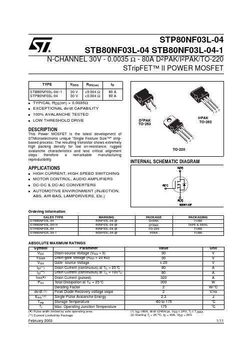
1/11February 2003.STP80NF03L-04STB80NF03L-04 STB80NF03L-04-1N-CHANNEL 30V - 0.0035 Ω - 80A D 2PAK/I 2PAK/TO-220STripFET™ II POWER MOSFETs TYPICAL R DS (on) = 0.0035Ωs EXCEPTIONAL dv/dt CAPABILITY s 100% AVALANCHE TESTED sLOW THRESHOLD DRIVEDESCRIPTIONThis Power MOSFET is the latest development of STMicroelectronis unique "Single Feature Size™" strip-based process. The resulting transistor shows extremely high packing density for low on-resistance, rugged avalanche characteristics and less critical alignment steps therefore a remarkable manufacturing reproducibility.APPLICATIONSs HIGH CURRENT, HIGH SPEED SWITCHING s MOTOR CONTROL, AUDIO AMPLIFIERS s DC-DC & DC-AC CONVERTERSs AUTOMOTIVE ENVIRONMENT (INJECTION, ABS, AIR-BAG, LAMPDRIVERS, Etc.)TYPEV DSS R DS(on)I D STB80NF03L-04/-1STP80NF03L-0430 V 30 V<0.004 Ω<0.004 Ω80 A 80 AOrdering InformationABSOLUTE MAXIMUM RATINGS(Pulse width limited by safe operating area.(**) Current Limited by Package(1) I SD ≤80A, di/dt ≤240A/µs, V DD ≤ 24V, T j ≤ T JMAX (2) Starting T j = 25 o C, I D = 40A, V DD = 20VSALES TYPEMARKING PACKAGE PACKAGINGSTB80NF03L-0480NF03L-04 @D 2PAK TUBE STB80NF03L-04T480NF03L-04 @D 2PAK TAPE & REELSTP80NF03L-0480NF03L-04 @TO-220TUBE STB80NF03L-04-180NF03L-04 @I 2PAKTUBESymbol Parameter Value Unit V DS Drain-source Voltage (V GS = 0)30V V DGRDrain-gate Voltage (R GS = 20 k Ω)30V V GS Gate- source Voltage± 20V I D (**)Drain Current (continuous) at T C = 25°C 80A I D (**)Drain Current (continuous) at T C = 100°C 80A I DM (•)Drain Current (pulsed)320A P tot Total Dissipation at T C = 25°C300W Derating Factor2W/°C dv/dt (1)Peak Diode Recovery voltage slope 2V/ns E AS (2)Single Pulse Avalanche Energy 2.3J T stg Storage Temperature -60 to 175°C T j Max. Operating Junction Temperature 175°CSTB80NF03L-04/-1/STP80NF03L-042/11THERMAL DATAELECTRICAL CHARACTERISTICS (T case = 25 °C unless otherwise specified)OFFON (*)DYNAMICRthj-case Rthj-ambT lThermal Resistance Junction-case Thermal Resistance Junction-ambientMaximum Lead Temperature For Soldering PurposeMax Max Typ0.562.5300°C/W °C/W °CSymbol ParameterTest ConditionsMin.Typ.Max.Unit V (BR)DSS Drain-sourceBreakdown Voltage I D = 250 µAV GS = 030V I DSSZero Gate VoltageDrain Current (V GS = 0)V DS = Max RatingV DS = Max Rating T C = 125°C 110µA µA I GSSGate-body Leakage Current (V DS = 0)V GS = ± 20 V±100nASymbol ParameterTest ConditionsMin.Typ.Max.Unit V GS(th)Gate Threshold Voltage V DS = V GS I D = 250 µA 1V R DS(on)Static Drain-source On ResistanceV GS = 10 V I D = 40 A V GS = 4.5 VI D = 40 A0.00350.0040.0040.0055ΩΩSymbol ParameterTest ConditionsMin.Typ.Max.Unit g fs (*)Forward Transconductance V DS = 15 VI D =15 A50S C iss C oss C rssInput Capacitance Output Capacitance Reverse Transfer CapacitanceV DS = 25V, f = 1 MHz, V GS = 055001670290pF pF pFSTB80NF03L-04/-1/STP80NF03L-04SWITCHING ONSWITCHING OFFSOURCE DRAIN DIODE(*)Pulsed: Pulse duration = 300 µs, duty cycle 1.5 %.(•)Pulse width limited by safe operating area.Symbol ParameterTest ConditionsMin.Typ.Max.Unit t d(on)t r Turn-on Delay Time Rise TimeV DD = 15 VI D = 40 A R G =4.7 Ω V GS = 4.5 V (Resistive Load, Figure 3)30270ns ns Q g Q gs Q gdTotal Gate Charge Gate-Source Charge Gate-Drain ChargeV DD =24V I D =80 A V GS =4.5V852340110nC nC nCSymbol ParameterTest ConditionsMin.Typ.Max.Unit t d(off)t f Turn-off Delay Time Fall TimeV DD = 15 VI D = 40 A R G =4.7Ω, V GS = 4.5 V (Resistive Load, Figure 3)11095ns ns t r(Voff)t f t cOff-Voltage Rise Time Fall TimeCross-over TimeV clamp = 24 VI D = 80 A R G =4.7Ω V GS = 4.5 V (Inductive Load, Figure 5)12575125ns ns nsSymbol ParameterTest ConditionsMin.Typ.Max.Unit I SD I SDM (•)Source-drain CurrentSource-drain Current (pulsed)80320A A V SD (*)Forward On Voltage I SD = 80 AV GS = 01.5V t rr Q rr I RRMReverse Recovery Time Reverse Recovery Charge Reverse Recovery CurrentI SD = 80 Adi/dt = 100A/µs V DD = 20 V T j = 150°C (see test circuit, Figure 5)750.154ns µC AELECTRICAL CHARACTERISTICS (continued)STB80NF03L-04/-1/STP80NF03L-04STB80NF03L-04/-1/STP80NF03L-04STB80NF03L-04/-1/STP80NF03L-046/11Fig. 3: Switching Times Test Circuits For ResistiveFig. 5: Test Circuit For Inductive Load Switching7/11STB80NF03L-04/-1/STP80NF03L-04DIM.mm.inch.MIN.TYP. MAX.MIN.TYP. TYP .A 4.4 4.60.1730.181A1 2.49 2.690.0980.106A20.030.230.0010.009B 0.70.930.0280.037B2 1.14 1.70.0450.067C 0.450.60.0180.024C2 1.21 1.360.0480.054D 8.959.350.3520.368D180.315E 1010.40.3940.409E18.50.334G 4.88 5.280.1920.208L 1515.850.5910.624L2 1.27 1.40.0500.055L3 1.4 1.750.0550.069M 2.43.20.0940.126R 0.40.015V20°8°0°8°D 2PAK MECHANICAL DATASTB80NF03L-04/-1/STP80NF03L-0410/11DIM.mm inchMIN.MAX.MIN.MAX.A010.510.70.4130.421B015.715.90.6180.626D 1.5 1.60.0590.063D1 1.59 1.610.0620.063E 1.65 1.850.0650.073F11.411.60.4490.456K0 4.8 5.00.1890.197P0 3.9 4.10.1530.161P111.912.10.4680.476P2 1.9 2.100750.082R50 1.574T0.250.35.0.00980.0137W23.724.30.9330.956DIM.mm inchMIN.MAX.MIN.MAX.A33012.992B 1.50.059C12.813.20.5040.520D20.20.795G24.426.40.960 1.039N100 3.937T30.4 1.197BASE QTY BULK QTY10001000REEL MECHANICAL DATA* on sales typeTUBE SHIPMENT (no suffix)* TAPE AND REEL SHIPMENT (suffix ”T4”)*D2PAK FOOTPRINTTAPE MECHANICAL DATA元器件交易网STB80NF03L-04/-1/STP80NF03L-04 Information furnished is believed to be accurate and reliable. However, STMicroelectronics assumes no responsibility for the consequencesof use of such information nor for any infringement of patents or other rights of third parties which may result from its use. No license is grantedby implication or otherwise under any patent or patent rights of STMicroelectronics. Specifications mentioned in this publication are subjectto change without notice. This publication supersedes and replaces all information previously supplied. STMicroelectronics products are notauthorized for use as critical components in life support devices or systems without express written approval of STMicroelectronics.The ST logo is registered trademark of STMicroelectronics® 2002 STMicroelectronics - All Rights ReservedAll other names are the property of their respective owners.STMicroelectronics GROUP OF COMPANIESAustralia - Brazil - Canada - China - Finland - France - Germany - Hong Kong - India - Israel - Italy - Japan - Malaysia - Malta - Morocco -Singapore - Spain - Sweden - Switzerland - United Kingdom - United States.11/11。
STPS60SM200CW;中文规格书,Datasheet资料
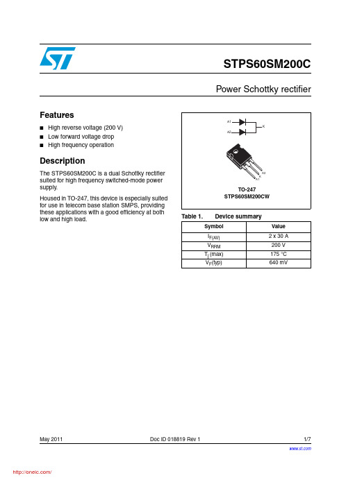
May 2011Doc ID 018819 Rev 11/7STPS60SM200CPower Schottky rectifierFeatures■High reverse voltage (200 V)■Low forward voltage drop ■High frequency operationDescriptionThe STPS60SM200C is a dual Schottky rectifier suited for high frequency switched-mode power supply.Housed in TO-247, this device is especially suited for use in telecom base station SMPS, providing these applications with a good efficiency at both low and high load.Table 1.Device summarySymbol Value I F(AV) 2 x 30 A V RRM 200 V T j (max)175 °C V F (typ)640 mVCharacteristics STPS60SM200C2/7Doc ID 018819 Rev 11 CharacteristicsWhen the two diodes 1 and 2 are used simultaneously:ΔT j (diode 1) = P(diode 1) x R th(j-c)(Per diode) + P(diode 2) x R th(c)To evaluate the conduction losses use the following equation: P = 0.58 x I F(AV) + 0.0037 x I F 2(RMS)Table 3.Thermal resistanceSymbol ParameterValue UnitR th(j-c)Junction to case Per diode 0.7°C/W Total0.5R th(c)Coupling0.3Table 4.Static electrical characteristics (per diode)Symbol ParameterTest conditions Min.Typ.Max.Unit I R (1)Reverse leakage currentT j = 25 °C V R = V RRM 0.05mAT j = 125 °C 613V F (2)Forward voltage dropT j = 25 °C I F = 7.5 A 0.670.70V T j = 125 °C 0.510.55T j = 25 °C I F = 15 A 0.730.77T j = 125 °C 0.570.61T j = 25 °C I F = 30 A0.790.83T j = 125 °C0.640.691.Pulse test: t p = 5 ms, δ < 2%2.Pulse test: t p = 380 µs, δ < 2%STPS60SM200CCharacteristicsDoc ID 018819 Rev 13/7Figure 1.Average forward power dissipation versus average forward current Figure 2.Average forward current versus ambient temperature (δ = 0.5)T= t /Tp t Figure 3.Non repetitive surge peak forward current versus overload duration Figure 4.Relative variation of thermalimpedance junction to case versus tFigure 5.Reverse leakage current versus reverse voltage applied Figure 6.Junction capacitance versus reverse voltage appliedCharacteristics STPS60SM200C4/7Doc ID 018819 Rev 1Figure 7.Forward voltage drop versus forward currentFigure 8.Forward voltage drop versus forward currentSTPS60SM200C Package informationDoc ID 018819 Rev 15/72 Package information●Epoxy meets UL94, V0●Cooling method: by conduction (C)●Recommended torque value: 0.55 to 1.0 N·mIn order to meet environmental requirements, ST offers these devices in different grades ofECOPACK ® packages, depending on their level of environmental compliance. ECOPACK ® specifications, grade definitions and product status are available at: . ECOPACK ® is an ST trademark.Ordering information STPS60SM200C6/7Doc ID 018819 Rev 13 Ordering information4 Revision historyTable 6.Ordering informationOrder code Marking Package Weight Base qty Delivery modeSTPS60SM200CWSTPS60SM200CWTO-2474.45 g30TubeTable 7.Document revision historyDate RevisionChanges17-May-20111First issue.STPS60SM200CPlease Read Carefully:Information in this document is provided solely in connection with ST products. STMicroelectronics NV and its subsidiaries (“ST”) reserve the right to make changes, corrections, modifications or improvements, to this document, and the products and services described herein at any time, without notice.All ST products are sold pursuant to ST’s terms and conditions of sale.Purchasers are solely responsible for the choice, selection and use of the ST products and services described herein, and ST assumes no liability whatsoever relating to the choice, selection or use of the ST products and services described herein.No license, express or implied, by estoppel or otherwise, to any intellectual property rights is granted under this document. If any part of this document refers to any third party products or services it shall not be deemed a license grant by ST for the use of such third party products or services, or any intellectual property contained therein or considered as a warranty covering the use in any manner whatsoever of such third party products or services or any intellectual property contained therein.UNLESS OTHERWISE SET FORTH IN ST’S TERMS AND CONDITIONS OF SALE ST DISCLAIMS ANY EXPRESS OR IMPLIED WARRANTY WITH RESPECT TO THE USE AND/OR SALE OF ST PRODUCTS INCLUDING WITHOUT LIMITATION IMPLIED WARRANTIES OF MERCHANTABILITY, FITNESS FOR A PARTICULAR PURPOSE (AND THEIR EQUIVALENTS UNDER THE LAWS OF ANY JURISDICTION), OR INFRINGEMENT OF ANY PATENT, COPYRIGHT OR OTHER INTELLECTUAL PROPERTY RIGHT. UNLESS EXPRESSLY APPROVED IN WRITING BY AN AUTHORIZED ST REPRESENTATIVE, ST PRODUCTS ARE NOT RECOMMENDED, AUTHORIZED OR WARRANTED FOR USE IN MILITARY, AIR CRAFT, SPACE, LIFE SAVING, OR LIFE SUSTAINING APPLICATIONS, NOR IN PRODUCTS OR SYSTEMS WHERE FAILURE OR MALFUNCTION MAY RESULT IN PERSONAL INJURY, DEATH, OR SEVERE PROPERTY OR ENVIRONMENTAL DAMAGE. ST PRODUCTS WHICH ARE NOT SPECIFIED AS "AUTOMOTIVE GRADE" MAY ONLY BE USED IN AUTOMOTIVE APPLICATIONS AT USER’S OWN RISK.Resale of ST products with provisions different from the statements and/or technical features set forth in this document shall immediately void any warranty granted by ST for the ST product or service described herein and shall not create or extend in any manner whatsoever, any liability of ST.ST and the ST logo are trademarks or registered trademarks of ST in various countries.Information in this document supersedes and replaces all information previously supplied.The ST logo is a registered trademark of STMicroelectronics. All other names are the property of their respective owners.© 2011 STMicroelectronics - All rights reservedSTMicroelectronics group of companiesAustralia - Belgium - Brazil - Canada - China - Czech Republic - Finland - France - Germany - Hong Kong - India - Israel - Italy - Japan - Malaysia - Malta - Morocco - Philippines - Singapore - Spain - Sweden - Switzerland - United Kingdom - United States of AmericaDoc ID 018819 Rev 17/7分销商库存信息: STMSTPS60SM200CW。
STP36NF06中文资料
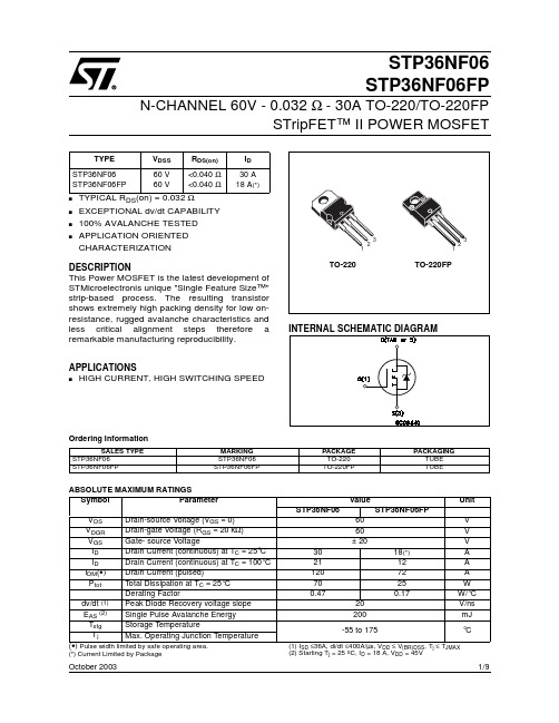
1/9October 2003STP36NF06STP36NF06FPN-CHANNEL 60V - 0.032 Ω - 30A TO-220/TO-220FPSTripFET™ II POWER MOSFETs TYPICAL R DS (on) = 0.032 Ωs EXCEPTIONAL dv/dt CAPABILITY s 100% AVALANCHE TESTED sAPPLICATION ORIENTED CHARACTERIZATIONDESCRIPTIONThis Power MOSFET is the latest development of STMicroelectronis unique "Single Feature Size™"strip-based process. The resulting transistor shows extremely high packing density for low on-resistance, rugged avalanche characteristics and less critical alignment steps therefore a remarkable manufacturing reproducibility.APPLICATIONSs HIGH CURRENT, HIGH SWITCHING SPEEDTYPE V DSS R DS(on)I D STP36NF06STP36NF06FP60 V 60 V<0.040 Ω<0.040 Ω30 A 18 A (*)Ordering InformationABSOLUTE MAXIMUM RATINGSPulse width limited by safe operating area.(*) Current Limited by Package(1) I SD ≤36A, di/dt ≤400A/µs, V DD ≤ V (BR)DSS , T j ≤ T JMAX (2) Starting T j = 25 o C, I D = 18 A, V DD = 45VSALES TYPEMARKING PACKAGE PACKAGINGSTP36NF06STP36NF06TO-220TUBE STP36NF06FPSTP36NF06FPTO-220FPTUBESymbol ParameterValueUnit STP36NF06STP36NF06FP V DS Drain-source Voltage (V GS = 0)60V V DGR Drain-gate Voltage (R GS = 20 k Ω)60V V GS Gate- source Voltage± 20V I D Drain Current (continuous) at T C = 25°C 3018(*)A I D Drain Current (continuous) at T C = 100°C 2112A I DM (•)Drain Current (pulsed)12072A P tot Total Dissipation at T C = 25°C 7025W Derating Factor0.470.17W/°C dv/dt (1)Peak Diode Recovery voltage slope 20V/ns E AS (2)Single Pulse Avalanche Energy 200mJ T stg Storage Temperature-55 to 175°CT jMax. Operating Junction TemperatureSTP36NF06 STP36NF06FP2/9THERMAL DATAELECTRICAL CHARACTERISTICS (T case = 25 °C unless otherwise specified)OFFON (*)DYNAMICTO-220TO-220FPRthj-case Thermal Resistance Junction-caseMax 2.146°C/W Rthj-ambT lThermal Resistance Junction-ambientMaximum Lead Temperature For Soldering Purpose (1.6 mm from case, for 10 sec)Max62.5300°C/W °CSymbol ParameterTest ConditionsMin.Typ.Max.Unit V (BR)DSS Drain-sourceBreakdown Voltage I D = 250 µA, V GS = 060V I DSSZero Gate VoltageDrain Current (V GS = 0)V DS = Max RatingV DS = Max Rating T C = 125°C 110µA µA I GSSGate-body Leakage Current (V DS = 0)V GS = ± 20 V±100nASymbol ParameterTest ConditionsMin.Typ.Max.Unit V GS(th)Gate Threshold Voltage V DS = V GS I D = 250 µA 2V R DS(on)Static Drain-source On ResistanceV GS = 10 VI D = 15 A0.0320.040ΩSymbol ParameterTest ConditionsMin.Typ.Max.Unit g fs (*)Forward Transconductance V DS = 25 VI D =15 A12S C iss C oss C rssInput Capacitance Output Capacitance Reverse Transfer CapacitanceV DS = 25V f = 1 MHz V GS = 069017068pF pF pF3/9STP36NF06 STP36NF06FPSWITCHING ONSWITCHING OFFSOURCE DRAIN DIODE(*)Pulsed: Pulse duration = 300 µs, duty cycle 1.5 %.(•)Pulse width limited by safe operating area.Symbol ParameterTest ConditionsMin.Typ.Max.Unit t d(on)t r Turn-on Delay Time Rise TimeV DD = 30 VI D = 18 A R G =4.7 Ω V GS = 10 V (Resistive Load, Figure 3)1040ns ns Q g Q gs Q gdTotal Gate Charge Gate-Source Charge Gate-Drain ChargeV DD = 30 V I D = 36 A V GS = 10V236931nC nC nCSymbol ParameterTest ConditionsMin.Typ.Max.Unit t d(off)t fTurn-off Delay Time Fall TimeV DD = 30 VI D = 18 A R G =4.7 Ω VGS =10 V (Resistive Load, Figure 3)279ns nsSymbol ParameterTest ConditionsMin.Typ.Max.Unit I SD I SDM (•)Source-drain CurrentSource-drain Current (pulsed)30120A A V SD (*)Forward On Voltage I SD = 30 AV GS = 01.5V t rr Q rr I RRMReverse Recovery Time Reverse Recovery Charge Reverse Recovery CurrentI SD = 30 Adi/dt = 100A/µs V DD = 30 V T j = 150°C (see test circuit, Figure 5)651554.8ns nC AELECTRICAL CHARACTERISTICS (continued)STP36NF06 STP36NF06FPSTP36NF06 STP36NF06FPSTP36NF06 STP36NF06FP6/9Fig. 3: Switching Times Test Circuits For ResistiveFig. 5: Test Circuit For Inductive Load SwitchingSTP36NF06 STP36NF06FP8/9DIM.mm.inch.MIN.TYP. MAX.MIN.TYP. TYP .A 4.4 4.60.1730.181C 1.23 1.320.0480.051D 2.40 2.720.0940.107E 0.490.700.0190.027F 0.610.880.0240.034F1 1.14 1.700.0440.067F2 1.14 1.700.0440.067G 4.95 5.150.1940.203G1 2.40 2.700.0940.106H21010.400.3930.409L216.400.645L328.901.137L413140.5110.551L5 2.65 2.950.1040.116L615.2515.750.6000.620L7 6.20 6.600.2440.260L9 3.50 3.930.1370.154DIA3.753.850.1470.151TO-220 MECHANICAL DATASTP36NF06 STP36NF06FP Information furnished is believed to be accurate and reliable. However, STMicroelectronics assumes no responsibility for the consequences of use of such information nor for any infringement of patents or other rights of third parties which may result from its use. No license is grantedby implication or otherwise under any patent or patent rights of STMicroelectronics. Specifications mentioned in this publication are subject to change without notice. This publication supersedes and replaces all information previously supplied. STMicroelectronics products are notauthorized for use as critical components in life support devices or systems without express written approval of STMicroelectronics.The ST logo is registered trademark of STMicroelectronicsAll other names are the property of their respective owners.® 2003 STMicroelectronics - All Rights ReservedSTMicroelectronics GROUP OF COMPANIESAustralia - Belgium - Brazil - Canada - China - Czech Republic - Finland - France - Germany - Hong Kong - India - Israel - Italy - Japan - Malaysia - Malta - Morocco -Singapore - Spain - Sweden - Switzerland - United Kingdom - United States.9/9。
STS3DNE60L;中文规格书,Datasheet资料
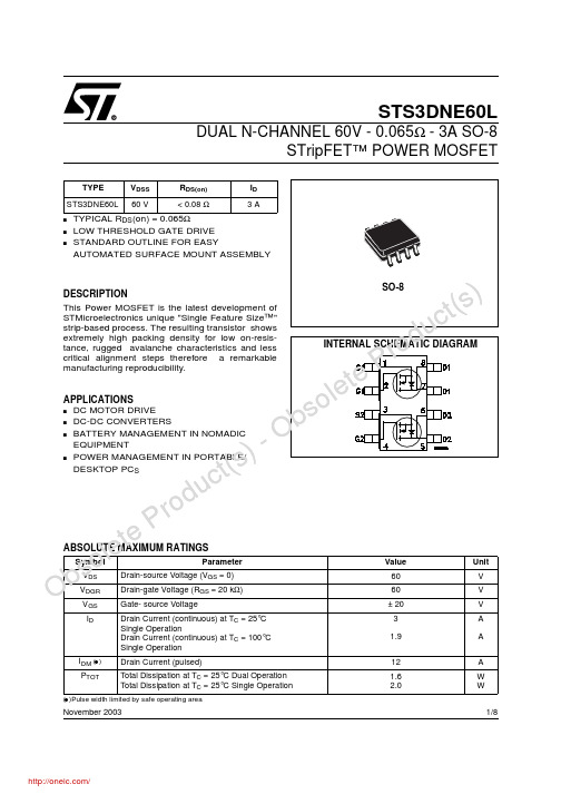
1/8November 2003STS3DNE60LDUAL N-CHANNEL 60V -0.065Ω -3A SO-8STripFET™POWERMOSFETs TYPICAL R DS (on)=0.065Ωs LOW THRESHOLD GATE DRIVE sSTANDARD OUTLINE FOR EASYAUTOMATED SURFACE MOUNT ASSEMBLYDESCRIPTIONThis Power MOSFET is the latest development of STMicroelectronics unique "Single Feature Size™"strip-based process.The resulting transistor shows extremely high packing density for low on-resis-tance,rugged avalanche characteristics and less critical alignment steps therefore a remarkable manufacturing reproducibility.APPLICATIONSs DC MOTOR DRIVE s DC-DC CONVERTERSs BATTERY MANAGEMENT IN NOMADIC EQUIPMENTs POWER MANAGEMENT IN PORTABLE/DESKTOP PC SABSOLUTE MAXIMUM RATINGS( )Pulsewidth limited by safe operating areaTYPE V DSS R DS(on)I D STS3DNE60L60V<0.08Ω3ASymbol ParameterValue Unit V DS Drain-source Voltage (V GS =0)60V V DGR Drain-gate Voltage (R GS =20k Ω)60V V GS Gate-source Voltage±20V I DDrain Current (continuous)at T C =25°C Single OperationDrain Current (continuous)at T C =100°C Single Operation 31.9A A I DM ( )Drain Current (pulsed)12A P TOTTotal Dissipation at T C =25°C Dual Operation Total Dissipation at T C =25°C Single Operation1.62.0W W l s Ob so e t ePr od u c t () -l t l c )Ob so e t ePr od u c (s )- O bs o e t eP r od u t (sSTS3DNE60L2/8THERMAL DATA(*)Mounted on FR-4Board (t ≤ 10 sec)ELECTRICAL CHARACTERISTICS (TCASE =25°C UNLESS OTHERWISE SPECIFIED)OFFON (1)DYNAMICRthj-amb(*)Thermal Resistance Junction-amb Max Single Operation (*)Thermal Resistance Junction-amb Max Dual Operation 62.578°C/W °C/W T j Max.Operating Junction Temperature 150°C T stgStorage Temperature–55to 150°CSymbol ParameterTest ConditionsMin.Typ.Max.Unit V (BR)DSS Drain-sourceBreakdown Voltage I D =250µA,V GS =060V I DSS Zero Gate VoltageDrain Current (V GS =0)V DS =Max Rating1µA V DS =Max Rating,T C =125°C 10µA I GSSGate-body Leakage Current (V DS =0)V GS =±20V±100nASymbol ParameterTest ConditionsMin.Typ.Max.Unit V GS(th)Gate Threshold Voltage V DS =V GS ,I D =250µA 1V R DS(on)Static Drain-source On ResistanceV GS =10V,I D =1.5A V GS =4.5V,I D =1.5A0.0650.080.080.1ΩΩSymbol ParameterTest ConditionsMin.Typ.Max.Unit g fs (1)Forward Transconductance V DS =15V ,I D =1.5A5S C iss Input Capacitance V DS =25V,f =1MHz,V GS =0815pF C oss Output Capacitance 125pF C rssReverse Transfer Capacitance40pFs l u )O() -O bs o e t eP r od c t(s3/8STS3DNE60LELECTRICAL CHARACTERISTICS (CONTINUED)SWITCHING ONSWITCHING OFFSOURCE DRAIN DIODENote: 1.Pulsed:Pulse duration =300µs,duty cycle 1.5%.2.Pulse width limited by safe operating area.Symbol ParameterTest ConditionsMin.Typ.Max.Unit t d(on)t r Turn-on Delay Time Rise TimeV DD =30V,I D =3A R G =4.7ΩV GS =5V (see test circuit,Figure 3)2030ns ns Q g Q gs Q gdTotal Gate Charge Gate-Source Charge Gate-Drain ChargeV DD =24V,I D =3A,V GS =4.5V13.563.5nC nC nCSymbol ParameterTest ConditionsMin.Typ.Max.Unit t r(off)t f t cOff-voltage Rise Time Fall TimeCross-over TimeV DD =48V,I D =3A R G =4.7Ω,V GS =5V (see test circuit,Figure 5)121632ns ns nsSymbol ParameterTest ConditionsMin.Typ.Max.Unit I SD Source-drain Current 3A I SDM (1)Source-drain Current (pulsed)12A V SD (2)Forward On Voltage I SD =3A,V GS =0 1.2V t rr Q rr I RRMReverse Recovery Time Reverse Recovery Charge Reverse Recovery CurrentI SD =3A,di/dt =100A/µs,V DD =30V,T j =150°C (see test circuit,Figure 5)601304ns nC AO-O STS3DNE60L4/8.Tranconductancellc Ob so e t eP-O bs o e t eP r od u t (5/8STS3DNE60LSource-drain Diode Forward Characteristics)osSTS3DNE60L6/8Fig.5:Test Circuit For Inductive Load Switching And Diode Recovery TimesFig.4:Gate Charge test CircuitFig.2:Unclamped Inductive WaveformFig.1:Unclamped Inductive Load Test CircuitFig.3:Switching Times Test Circuit For Resistive LoadSTS3DNE60L7/8l slc)O b s oe t eP ro du ct()-O bs oe t eP ro dut(sSTS3DNE60L8/8Information furnished is believed to be accurate and reliable. However, STMicroelectronics assumes no responsibility for the consequences of use of such information nor for any infringement of patents or other rights of third parties which may result from its use. No license is granted by implication or otherwise under any patent or patent rights of STMicroelectronics. Specifications mentioned in this publication are subject to change without notice. This publication supersedes and replaces all information previously supplied. STMicroelectronics products are not authorized for use as critical components in life support devices or systems without express written approval of STMicroelectronics.© The ST logo is a registered trademark of STMicroelectronics© 2003 STMicroelectronics - Printed in Italy - All Rights ReservedSTMicroelectronics GROUP OF COMPANIESAustralia - Brazil - Canada - China - Finland - France - Germany - Hong Kong - India - Israel - Italy - Japan - Malaysia - Malta - Morocco Singapore - Spain - Sweden - Switzerland - United Kingdom - United States.© 分销商库存信息: STMSTS3DNE60L。
NCP603中文资料

2
元器件交易网
NCP603
ELECTRICAL CHARACTERISTICS (Vin = 1.750 V, Vout = 1.250 V, Cin = Cout =1.0 mF, for typical values TA = 25°C, for min/max
Typical Applications
•ăSMPS Post-Regulation •ăHand-held Instrumentation & Audio Players •ăNoise Sensitive Circuits – VCO, RF Stages, etc. •ăCamcorders and Cameras •ăPortable Computing
ESD Human Body Model tested per AEC-Q100-002 (EIA/JESD22-A114) ESD Machine Model tested per AEC-Q100-003 (EIA/JESD22-A115) Latchup Current Maximum Rating: v150 mA per JEDEC standard: JESD78.
-
62 55 38
-
Line Regulation
Load Regulation Output Noise Voltage (Note 9) Output Short Circuit Current Dropout Voltage
1.25 V
Dropout Voltage 1.25 V
Regline
THERMAL CHARACTERISTICS
Rating
Thermal Characteristics, TSOP-5 (Note 4) Thermal Resistance, Junction-to-Air (Note 5)
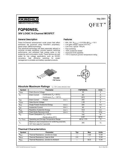
FQP60N03L中文资料
td(on)
Turn-On Delay Time
tr
Turn-On Rise Time
td(off)
Turn-Off Delay Time
tf
Turn-Off Fall Time
Qg
Total Gate Charge
Qgs
Gate-Source Charge
Qgd
Gate-Drain Charge
VDD = 15 V, ID = 30 A, RG = 25 Ω
Test Conditions
Min Typ Max Units
Off Characteristics
BVDSS ∆BVDSS / ∆TJ
Drain-Source Breakdown Voltage
Breakdown Voltage Temperature Coefficient
IDSS
Zero Gate Voltage Drain Current
©2001 Fairchild Semiconductor Corporation
Rev. A1. May 2001
FQP60N03L
元器件交易网
Electrical Characteristics
Symbol
Parameter
TC = 25°C unless otherwise noted
V25DS0μ=s15PVulse
Test
100
0
2
4
6
8
10
V , Gate-Source Voltage [V] GS
Figure 2. Transfer Characteristics
102
101
100 0.2
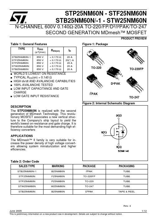
STP25NM60N中文资料
1/12PRODUCT PREVIEWJune 2005This is preliminary information on a new product now in development. Details are subject to change without notice.STP25NM60N - STF25NM60N STB25NM60N/-1 - STW25NM60NSECOND GENERATION MDmesh™ MOSFETTable 1: General Featuress WORLD’S LOWEST ON RESISTANCE s TYPICAL R DS (on) = 0.140 Ωs HIGH dv/dt AND AVALANCHE CAPABILITIES s 100% AVALANCHE TESTEDsLOW INPUT CAPACITANCE AND GATE CHARGEsLOW GATE INPUT RESISTANCEDESCRIPTIONThe STP25NM60N is realized with the second generation of MDmesh Technology. This revolu-tionary MOSFET associates a new vertical struc-ture to the Company's strip layout to yield the world's lowest on-resistance and gate charge. It is therefore suitable for the most demanding high ef-ficiency convertersAPPLICATIONSThe MDmesh™ II family is very suitable for in-crease the power density of high voltage convert-ers allowing system miniaturization and higher efficiencies.Table 2: Order CodeTYPE V DSS (@Tjmax)R DS(on)I D STB25NM60N-1STF25NM60N STP25NM60N STW25NM60N STB25NM60N650 V 650 V 650 V 650 V 650 V< 0.170 Ω< 0.170 Ω< 0.170 Ω< 0.170 Ω< 0.170 Ω20 A 20(*) A 20 A 20 A 20 ASALES TYPE MARKING PACKAGE PACKAGINGSTB25NM60N-1B25NM60N I ²PAK TUBE STF25NM60N F25NM60N TO-220FP TUBE STP25NM60N P25NM60N TO-220TUBE STW25NM60N W25NM60N TO-247TUBE STB25NM60NB25NM60ND ²PAKTAPE & REELRev. 4STP25NM60N - STF25NM60N - STB25NM60N/-1 - STW25NM60N2/12Table 3: Absolute Maximum ratings(*) Limited only by maximum temperature allowed (1) Pulse width limited by safe operating area(2) I SD ≤ 20 A, di/dt ≤ 400 A/µs, V DD =80%V (BR)DSS .Table 4: Thermal DataTable 5: Avalanche CharacteristicsELECTRICAL CHARACTERISTICS (T CASE =25°C UNLESS OTHERWISE SPECIFIED)Table 6: On /Off(2) Characteristic value at turn off on inductive loadSymbolParameterValueUnitTO-220/I²PAK TO-247/D²PAKTO-220FPV DS Drain-source Voltage (V GS = 0)600V V DGR Drain-gate Voltage (R GS = 20 k Ω)600V V GS Gate- source Voltage± 25V I D Drain Current (continuous) at T C = 25°C 2020 (*)A I D Drain Current (continuous) at T C = 100°C 12.812.8 (*)A I DM (1)Drain Current (pulsed)8080 (*)A P TOT Total Dissipation at T C = 25°C 16040W Derating Factor1.280.32W/°C dv/dt (2)Peak Diode Recovery voltage slope TBD V/ns T stg Storage Temperature– 55 to 150°C T jMax. Operating Junction Temperature150°C TO-220/I²PAK TO-247/D²PAKTO-220FPRthj-case Thermal Resistance Junction-case Max 0.783.1°C/W Rthj-ambThermal Resistance Junction-ambient Max62.5°C/W T lMaximum Lead Temperature For Soldering Purpose300°CSymbol ParameterMax Value Unit I AS Avalanche Current, Repetitive or Not-Repetitive (pulse width limited by T j max)TBD A E ASSingle Pulse Avalanche Energy(starting T j = 25 °C, I D = I AS , V DD = 50 V)TBDmJSymbol ParameterTest ConditionsValue UnitMin.Typ.Max.V (BR)DSS Drain-source Breakdown VoltageI D = 1 mA, V GS = 0600V dv/dt(2)Drain Source Voltage SlopeVdd=TBD, Id=TBD, Vgs=TBD TBDV/ns I DSS Zero Gate VoltageDrain Current (V GS = 0)V DS = Max RatingV DS = Max Rating, T C = 125°C 110µA µA I GSS Gate-body Leakage Current (V DS = 0)V GS = ± 20 V100nA V GS(th)Gate Threshold Voltage V DS = V GS , I D = 250 µA 234V R DS(onStatic Drain-source On ResistanceV GS = 10 V, I D = 10 A0.1400.170Ω3/12STP25NM60N - STF25NM60N - STB25NM60N/-1 - STW25NM60NELECTRICAL CHARACTERISTICS (CONTINUED)Table 7: DynamicTable 8: Source Drain Diode(1) Pulsed: Pulse duration = 300 µs, duty cycle 1.5 %.(2) Pulse width limited by safe operating area.(3) C oss eq. is defined as a constant equivalent capacitance giving the same charging time as C oss when V DS increases from 0 to 80% V DSS .Symbol ParameterTest Conditions Min.Typ.Max.Unit g fs (1)Forward Transconductance V DS = 15V , I D = 10A 17S C iss C oss C rss Input Capacitance Output Capacitance Reverse Transfer Capacitance V DS = 25 V, f = 1 MHz, V GS = 0256551177pF pF pF C OSS eq (3).Equivalent Output CapacitanceV GS = 0 V, V DS = 0 to 480 V TBD pF R GGate Input Resistancef=1 MHz Gate DC Bias = 0Test Signal Level = 20mV Open Drain2Ωt d(on)t r t d(off)t f Turn-on Delay Time Rise TimeTurn-off-Delay Time Fall TimeV DD = 300 V, I D = 10 A, R G = 4.7 Ω, V GS = 10 V (see Figure 4)TBD TBD TBD TBD ns ns ns ns Q g Q gs Q gdTotal Gate Charge Gate-Source Charge Gate-Drain ChargeV DD = 480 V, I D = 20 A,V GS = 10 V (see Figure 7)93TBD TBDnC nC nCSymbol ParameterTest ConditionsMin.Typ.Max.Unit I SD I SDM (2)Source-drain CurrentSource-drain Current (pulsed)2080A A V SD (1)Forward On Voltage I SD = 20 A, V GS = 0 1.3V t rr Q rr I RRM Reverse Recovery Time Reverse Recovery Charge Reverse Recovery Current I SD = 25 A, di/dt = 100 A/µs V DD = 100V (see Figure 5)TBD TBD TBD ns µC A t rr Q rr I RRMReverse Recovery Time Reverse Recovery Charge Reverse Recovery CurrentI SD = 25 A, di/dt = 100 A/µs V DD = 100V, T j = 150°C (see Figure 5)TBD TBD TBDns µC ASTP25NM60N - STF25NM60N - STB25NM60N/-1 - STW25NM60NFigure 3: Unclamped Inductive Load Test Cir-cuitFigure 4: Switching Times Test Circuit For Re-sistive Load Figure 5: Test Circuit For Inductive Load Switching and Diode Recovery TimesFigure 6: Unclamped Inductive WafeformFigure 7: Gate Charge Test CircuitSTP25NM60N - STF25NM60N - STB25NM60N/-1 - STW25NM60N5/12STP25NM60N - STF25NM60N - STB25NM60N/-1 - STW25NM60N6/12STP25NM60N - STF25NM60N - STB25NM60N/-1 - STW25NM60N7/12STP25NM60N - STF25NM60N - STB25NM60N/-1 - STW25NM60N8/12STP25NM60N - STF25NM60N - STB25NM60N/-1 - STW25NM60N9/12STP25NM60N - STF25NM60N - STB25NM60N/-1 - STW25NM60N10/12TAPE AND REEL SHIPMENTD2PAK FOOTPRINT* on sales typeDIM.mm inchMIN.MAX.MIN.MAX.A33012.992B 1.50.059C12.813.20.5040.520D20.20795G24.426.40.960 1.039N100 3.937T30.4 1.197BASE QTY BULK QTY10001000REEL MECHANICAL DATA DIM.mm inchMIN.MAX.MIN.MAX.A010.510.70.4130.421B015.715.90.6180.626D 1.5 1.60.0590.063D1 1.59 1.610.0620.063E 1.65 1.850.0650.073F11.411.60.4490.456K0 4.8 5.00.1890.197P0 3.9 4.10.1530.161P111.912.10.4680.476P2 1.9 2.10.0750.082R50 1.574T0.250.350.00980.0137W23.724.30.9330.956TAPE MECHANICAL DATASTP25NM60N - STF25NM60N - STB25NM60N/-1 - STW25NM60N Table 9: Revision HistoryDate Revision Description of Changes 30-Nov-20041First Release.22-Mar-20052Modified title23-May-20053Inserted some values in Tab708-Jun-20054Inserted new row in table 611/12STP25NM60N - STF25NM60N - STB25NM60N/-1 - STW25NM60NInformation furnished is believed to be accurate and reliable. However, STMicroelectronics assumes no responsibility for the consequences of use of such information nor for any infringement of patents or other rights of third parties which may result from its use. No license is granted by implication or otherwise under any patent or patent rights of STMicroelectronics. Specifications mentioned in this publication are subject to change without notice. This publication supersedes and replaces all information previously supplied. STMicroelectronics products are not authorized for use as critical components in life support devices or systems without express written approval of STMicroelectronics.The ST logo is a registered trademark of STMicroelectronicsAll other names are the property of their respective owners© 2005 STMicroelectronics - All Rights ReservedSTMicroelectronics group of companiesAustralia - Belgium - Brazil - Canada - China - Czech Republic - Finland - France - Germany - Hong Kong - India - Israel - Italy - Japan - Malaysia - Malta - Morocco - Singapore - Spain - Sweden - Switzerland - United Kingdom - United States of America12/12。
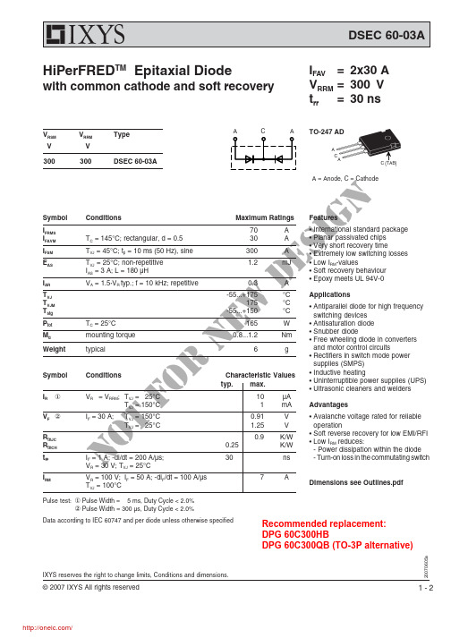
DSEC60-03A;中文规格书,Datasheet资料
Conditions
or VR = VRRM; TVJ = 25°C TVJ = 150°C
f IF = 30 A; TVJ = 150°C
TVJ = 25°C
ot IF = 1 A; -di/dt = 200 A/µs; NVR = 30 V; TVJ = 25°C
10
µA
1 mA Advantages
0.91
V
• Avalanche voltage rated for reliable
1.25
V
operation
0.25
0.9
K/W K/W
• Soft reverse recovery for low EMI/RFI • Low IRM reduces:
- Power dissipation within the diode
.+175
°C
175
°C
-55...+150
°C
w165
W
e0.8...1.2
Nm
n6
g
Applications
• Antiparallel diode for high frequency switching devices
• Antisaturation diode • Snubber diode • Free wheeling diode in converters
DSEC 60-03A
HiPerFREDTM Epitaxial Diode
with common cathode and soft recovery
IFAV = 2x30 A VRRM = 300 V trr = 30 ns
西门子3AC最小油电路断路器中级电压服务技术简介说明书

Retrofit Solution for SIEMENS 3AC make minimum oil circuit breakerThe foremost advantage of retrofittinga circuit breaker in switchgear is thatthe required specifications are metwith the latest technology at only apartial cost of replacing the equipment.This becomes more evident whenthe associated costs of civil works,cabling and downtime are considered.Retrofitting helps in saving up to 60percent of the cost of new equipment.Typically, retrofitting constitutesreplacement of vital equipment havingsimilar or advanced features, for lifeextension, reduced maintenance andimproved functionality. This includesupgradation and modernization ofbasic equipment and allied parts. Theretrofitted switchgear offers far greatersystem, reliability, long term safety andlong term availability of spares withminimal investment and downtime.Siemens 3AC breakerABB is a full system provider forretrofit solutions, from the proposaland design, through the manufacturingand testing, up to the installation andcommissioning.1V Y N 000006 R e v . 00, e n - C o p y r i g h t © 2014 A B B . A l l r i g h t s r e s e r v e d .For more information please contact Service department at: ABB India LimitedPPMV – Retrofit & Services Plot No. 79, Street No. 17,MIDC Estate,Satpur Nashik,Maharashtra, India – 422007Tel: +91 253-2201200Fax: +91 253-2351260Email:******************.com ABB VD4 retrofit of Siemens 3AC breakerNOTE:We reserve the right to make changes in the course of technical development.Benefits Reliability– Significant life time extension– Lower maintenance requirements – Long time availability of spare parts Safety– Strong fault risk reduction– Additional embedded safety features – Improved operator protection Technology– Latest generation apparatus– Designed according to IEC 62271-100 Standard – Tested and certified products Project– Short implementation time for replacement – Minimum shutdown of the switchboard – Smooth site activity Investment– Limited capital investment– Minimization of further maintenance costs – Warranty on the conversion workFactsThese circuit breakers are widely present in the networks and ABB can provide the relevant retrofitting solutions across the globe. This equipment has been in service for many decades and retrofitting could significantly extend the operational life of the switchgear. The use of well proven VD4 Vacuum circuit breaker enhances the reliability of the switchgear. The retrofit circuit breakers can be fitted with Surge Arresters or Potential Transformers on request. Many types of existing circuitbreakers can be identified by looking at the rating plates Viz. 3AC-10NTechnical dataA full range of retrofit solutions have been developed based on ABB vacuum and gas circuit breakers. Fused vacuum contactor is also available for replacing Motor Starter Units.ABB proposal provides the best fit for purpose apparatus for each switchgear unit, depending of the complete network, equipment conditions and the specific feeder operational characteristics.The following basic details are necessary for providing standard retrofit solutions:– Height, width and depth of the circuit breaker compartment – GA, cross section and schematic drawing of the existing panel– Height, width and depth of the panel – Control & motor voltage – Feeder details。
2N60-TN3-T中文资料(Unisonic Technologies)中文数据手册「EasyDatasheet - 矽搜」
VGS
作为D.U.T.
* D.U.T.-测试设备
图 . 1A峰值二极管恢复 dv / dt测试电路
期
P.W.
P. W. D= 期
VGS= 10V
I FM,体二极管正向电流
di/dt IRM
体二极管反向电流
体二极管恢复dv
/dt
VDD
体二极管
正向压降
图 . 1B峰值二极管恢复 dv / dt波形
芯片中文手册,看全文,戳
△BV DSS/ △ TJ
ID = 250 µA
VGS(TH) RDS(ON)
gFS
VDS = VGS, ID = 250µA VGS = 10V, I D =1A VDS = 50V, I D = 1A(注1)
CISS COSS CRSS
VDS =25V, V GS =0V, f =1MHz
功 率 M OSFET
注:1.脉冲测试:脉冲宽度 2.基本上是独立工作温度
功 率 M OSFET
符号
测试条件
MIN TYP MAX 单元
tD (ON) tR
tD(OFF) tF QG
Q GS Q GD
VDD =300V, I D =2.4A, R G=25Ω (注1,2)
V DS=480V, V GS=10V, I D=2.4A (注1,2)
2N60
测试电路和波形(续)
V V R
10V
R V
D.U.T.
图 . 2A开关测试电路
功 率 M OSFET
V
90%
10% V
t t
t t
图 . 2B开关波形
同类型
50kΩ
作为D.U.T.
STP60NF06L中文资料
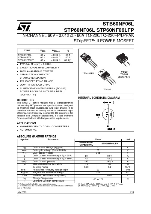
1/11July 2003.STB60NF06LSTP60NF06L STP60NF06LFPN-CHANNEL 60V - 0.012 Ω - 60A TO-220/TO-220FP/D 2PAKSTripFET™ II POWER MOSFETs TYPICAL R DS (on) = 0.012Ωs EXCEPTIONAL dv/dt CAPABILITY s 100% AVALANCHE TESTED sAPPLICATION ORIENTED CHARACTERIZATIONs 175 o C OPERATING RANGE s LOW THRESHOLD DRIVEsSURFACE-MOUNTING D 2PAK (TO-263) POWER PACKAGE IN TAPE & REEL (SUFFIX “T4”)DESCRIPTIONThis MOSFET series realized with STMicroelectronics unique STripFET process has specifically been designed to minimize input capacitance and gate charge. It is therefore suitable as primary switch in advanced high-efficiency, high-frequency isolated DC-DC converters for Telecom and Computer applications. It is also intended for any applications with low gate drive requirements.APPLICATIONSs HIGH-EFFICIENCY DC-DC CONVERTERS s AUTOMOTIVETYPE V DSS R DS(on)I D STB60NF06L STP60NF06L STP60NF06LFP60 V 60 V 60 V<0.014 Ω<0.014 Ω<0.014 Ω60 A 60 A 60 A(*)ABSOLUTE MAXIMUM RATINGSPulse width limited by safe operating area.(*) Refer to SOA for the max allowable current values on FP-type due to Rth value(1)I SD ≤ 60A, di/dt ≤ 600A/µs, V DD ≤ 48V, T j ≤ T JMAX.(2) Starting T j = 25 o C, I D = 30A, V DD = 30VSymbol ParameterValueUnitSTB60NF06L STP60NF06LSTP60NF06LFP V DS Drain-source Voltage (V GS = 0)60V V DGR Drain-gate Voltage (R GS = 20 k Ω)60V V GS Gate- source Voltage± 15V I D Drain Current (continuous) at T C = 25°C 6060(*)A I D Drain Current (continuous) at T C = 100°C 4242(*)A I DM (•)Drain Current (pulsed)240240(*)A P tot Total Dissipation at T C = 25°C 11030W Derating Factor0.730.2W/°C dv/dt (1)Peak Diode Recovery voltage slope 20V/ns E AS (2)Single Pulse Avalanche Energy 320mJ V ISO Insulation Withstand Voltage (DC)------2000V T stg Storage Temperature-55 to 175°CT jOperating Junction TemperatureSTB60NF06L STP60NF06L/FP2/11THERMAL DATA(#)Only for SMD, When Mounted on 1 inch 2 FR-4 board, 2 oz of Cu.ELECTRICAL CHARACTERISTICS (T case = 25 °C unless otherwise specified)OFFON (1)DYNAMICD 2PAK TO-220TO-220FPRthj-case Thermal Resistance Junction-caseMax 1.365.0°C/W Rthj-amb Rthj-pcb T lThermal Resistance Junction-ambient Thermal Resistance Junction-pcb (#)Maximum Lead Temperature For Soldering PurposeMax Max62.535300°C/W °C/W °CSymbol ParameterTest ConditionsMin.Typ.Max.Unit V (BR)DSS Drain-sourceBreakdown Voltage I D = 250 µA, V GS = 060V I DSSZero Gate VoltageDrain Current (V GS = 0)V DS = Max RatingV DS = Max Rating T C = 125°C 110µA µA I GSSGate-body Leakage Current (V DS = 0)V GS = ± 15V±100nASymbol ParameterTest ConditionsMin.Typ.Max.Unit V GS(th)Gate Threshold Voltage V DS = V GS I D = 250 µA 1V R DS(on)Static Drain-source On ResistanceV GS = 5 V I D = 30 A V GS = 10 VI D = 30 A0.0140.0120.0160.014ΩΩSymbol ParameterTest ConditionsMin.Typ.Max.Unit g fs (*)Forward Transconductance V DS = 15 VI D =30 A20S C iss C oss C rssInput Capacitance Output Capacitance Reverse Transfer CapacitanceV DS = 25V, f = 1 MHz, V GS = 02000360125pF pF pF3/11STB60NF06L STP60NF06L/FPSWITCHING ONSWITCHING OFFSOURCE DRAIN DIODEPulsed: Pulse duration = 300 µs, duty cycle 1.5 %.(•)Pulse width limited by safe operating area.Symbol ParameterTest ConditionsMin.Typ.Max.Unit t d(on)t r Turn-on Delay Time Rise TimeV DD = 30 VI D = 30 A R G =4.7 Ω V GS = 4.5 V (Resistive Load, Figure 3)35220ns ns Q g Q gs QgdTotal Gate Charge Gate-Source Charge Gate-Drain ChargeV DD = 48 V I D = 60 A V GS = 4.5V351020nC nC nCSymbol ParameterTest ConditionsMin.Typ.Max.Unit t d(off)t fTurn-off Delay Time Fall TimeV DD = 30VI D = 30 A R G =4.7Ω,V GS = 4.5 V (Resistive Load, Figure 3)5530ns nsSymbol ParameterTest ConditionsMin.Typ.Max.Unit I SD I SDM (•)Source-drain CurrentSource-drain Current (pulsed)60240A A V SD (*)Forward On Voltage I SD = 60AV GS = 01.3V t rr Q rr I RRMReverse Recovery Time Reverse Recovery Charge Reverse Recovery CurrentI SD = 60 Adi/dt = 100A/µs V DD = 30 V T j = 150°C (see test circuit, Figure 5)1102504.5ns nC AELECTRICAL CHARACTERISTICS (continued)STB60NF06L STP60NF06L/FPSTB60NF06L STP60NF06L/FPSTB60NF06L STP60NF06L/FP6/11Fig. 3: Switching Times Test Circuits For ResistiveFig. 5: Test Circuit For Inductive Load Switching7/11STB60NF06L STP60NF06L/FPDIM.mm.inch.MIN.TYP. MAX.MIN.TYP. TYP .A 4.4 4.60.1730.181A1 2.49 2.690.0980.106A20.030.230.0010.009B 0.70.930.0280.037B2 1.14 1.70.0450.067C 0.450.60.0180.024C2 1.21 1.360.0480.054D 8.959.350.3520.368D180.315E 1010.40.3940.409E18.50.334G 4.88 5.280.1920.208L 1515.850.5910.624L2 1.27 1.40.0500.055L3 1.4 1.750.0550.069M 2.43.20.0940.126R 0.40.015V20°8°0°8°D 2PAK MECHANICAL DATA9/11STB60NF06L STP60NF06L/FPDIM.mm.inch.MIN.TYP. MAX.MIN.TYP. TYP .A 4.4 4.60.1730.181C 1.23 1.320.0480.051D 2.40 2.720.0940.107E 0.490.700.0190.027F 0.610.880.0240.034F1 1.14 1.700.0440.067F2 1.14 1.700.0440.067G 4.95 5.150.1940.203G1 2.40 2.700.0940.106H21010.400.3930.409L216.400.645L328.901.137L413140.5110.551L5 2.65 2.950.1040.116L615.2515.750.6000.620L7 6.20 6.600.2440.260L9 3.50 3.930.1370.154DIA3.753.850.1470.151TO-220 MECHANICAL DATASTB60NF06L STP60NF06L/FP10/11DIM.mm inchMIN.MAX.MIN.MAX.A010.510.70.4130.421B015.715.90.6180.626D 1.5 1.60.0590.063D1 1.59 1.610.0620.063E 1.65 1.850.0650.073F11.411.60.4490.456K0 4.8 5.00.1890.197P0 3.9 4.10.1530.161P111.912.10.4680.476P2 1.9 2.100750.082R50 1.574T0.250.35.0.00980.0137W23.724.30.9330.956DIM.mm inchMIN.MAX.MIN.MAX.A33012.992B 1.50.059C12.813.20.5040.520D20.20.795G24.426.40.960 1.039N100 3.937T30.4 1.197BASE QTY BULK QTY10001000REEL MECHANICAL DATA* on sales typeTUBE SHIPMENT (no suffix)* TAPE AND REEL SHIPMENT (suffix ”T4”)*D2PAK FOOTPRINTTAPE MECHANICAL DATA元器件交易网STB60NF06L STP60NF06L/FP Information furnished is believed to be accurate and reliable. However, STMicroelectronics assumes no responsibility for the consequencesof use of such information nor for any infringement of patents or other rights of third parties which may result from its use. No license is grantedby implication or otherwise under any patent or patent rights of STMicroelectronics. Specifications mentioned in this publication are subjectto change without notice. This publication supersedes and replaces all information previously supplied. STMicroelectronics products are notauthorized for use as critical components in life support devices or systems without express written approval of STMicroelectronics.The ST logo is registered trademark of STMicroelectronics® 2002 STMicroelectronics - All Rights ReservedAll other names are the property of their respective owners.STMicroelectronics GROUP OF COMPANIESAustralia - Brazil - Canada - China - Finland - France - Germany - Hong Kong - India - Israel - Italy - Japan - Malaysia - Malta - Morocco -Singapore - Spain - Sweden - Switzerland - United Kingdom - United States.11/11。
NCP603SN280T1G,NCP603SN300T1G,NCP603SN330T1G,NCP603SN350T1G,NCP603SN500T1G, 规格书,Datasheet 资料

1. True no connect. Printed circuit board traces are allowable.
ABSOLUTE MAXIMUM RATINGS
Rating
Symbol
Value
Unit
Input Voltage (Note 2) Output, Enable, Adjustable Voltage
Dropout Voltage 1.25 V
Regload Iout = 1.0 mA to 300 mA
−
2.0
45
mV
Vn
f = 10 Hz to 100 kHz
−
50
−
mVrms
Isc
350
650
900
mA
VDO
Measured at: Vout – 2.0%,
Iout = 150 mA, Figure 2
VIN GND
Fixed Voltage Only
Driver w/ Current Limit
Thermal Shutdown
+ -
+ −1.25 V
Adjustable Version Only
ENABLE Figure 1. Simplified Block Diagram
VOUT ADJ
PIN CONNECTIONS
Vin 1 GND 2 ENABLE 3
5 Vout 4 ADJ/NC*
(Top View)
* ADJ − Adjustable Version * NC − Fixed Voltage Version
ORDERING INFORMATION
STGW30NC60VD;中文规格书,Datasheet资料

February 2011Doc ID 13241 Rev 51/13STGW30NC60VD40 A, 600 V , very fast IGBT with Ultrafast diodeFeatures■High current capability■High frequency operation up to 50 KHz ■Very soft ultra fast recovery antiparallel diodeApplications■High frequency inverters, UPS ■Motor drive■SMPS and PFC in both hard switch and resonant topologiesDescriptionThis device utilizes the advanced Power MESH™ process resulting in an excellent trade-offbetween switching performance and low on-state behavior.Table 1.Device summaryOrder code Marking Package Packaging STGW30NC60VDGW30NC60VDTO-247 long leadsT ubeContents STGW30NC60VDContents1Electrical ratings . . . . . . . . . . . . . . . . . . . . . . . . . . . . . . . . . . . . . . . . . . . . 32Electrical characteristics . . . . . . . . . . . . . . . . . . . . . . . . . . . . . . . . . . . . . 42.1Electrical characteristics (curves) . . . . . . . . . . . . . . . . . . . . . . . . . . . 6 3Test circuits . . . . . . . . . . . . . . . . . . . . . . . . . . . . . . . . . . . . . . . . . . . . . . . 9 4Package mechanical data . . . . . . . . . . . . . . . . . . . . . . . . . . . . . . . . . . . . 10 5Revision history . . . . . . . . . . . . . . . . . . . . . . . . . . . . . . . . . . . . . . . . . . . 122/13Doc ID 13241 Rev 5STGW30NC60VD Electrical ratingsDoc ID 13241 Rev 53/131 Electrical ratingsTable 2.Absolute maximum ratingsSymbol ParameterValue Unit V CES Collector-emitter voltage (V GE = 0)600V I C (1)1.Calculated according to the iterative formula:Continuous collector current at T C = 25 °C 80A I C (1)Continuous collector current at T C = 100 °C 40A I CP (2)2.Pulse width limited by maximum junction temperature and turn-off within RBSOA Pulsed collector current 150A I CL (3)3.V clamp = 80 % V CES , T J = 150 °C, R G = 10 Ω, V GE = 15 VTurn-off latching current 100A V GE Gate-emitter voltage± 20V I F Diode RMS forward current at T C = 25 °C 30A I FSM Surge not repetitive forward currentt P = 10 ms sinusoidal 120A P TOT Total dissipation at T C = 25 °C 250W T J Operating junction temperature – 55 to 150°C T STG Storage temperatureT LMaximum lead temperature for soldering purpose for 10 sec300°CTable 3.Thermal dataSymbol ParameterValue Unit R thJC Thermal resistance junction-case IGBT 0.5°C/W Thermal resistance junction-case diode 1.5°C/W R thJAThermal resistance junction-ambient50°C/WI C T C ()T j max ()T C–R thj c –V CE sat ()max ()T j max ()I C T C (),()×-------------------------------------------------------------------------------------------------------=Electrical characteristics STGW30NC60VD4/13Doc ID 13241 Rev 52 Electrical characteristicsT J = 25 °C unless otherwise specified.Table 4.StaticSymbol ParameterTest conditionsMin.Typ.Max.UnitV (BR)CESCollector-emitter breakdownvoltage (V GE = 0)I C = 1 mA600VV CE(sat)Collector-emitter saturation voltage V GE = 15 V , I C =20 AV GE = 15 V , I C =40 A V GE = 15 V , I C =80 A,T j =100 °CV GE = 15 V , I C =20 A,T j =125 °C 1.82.12.91.72.5VV GE(th)Gate threshold voltage V CE = V GE , I C = 250 µA 3.755.75V I CES Collector-cut-off current (V GE = 0)V CE = 600 VV CE = 600 V , T j = 125 °C 101µA mA I GESGate-emitter leakage current (V CE = 0)V GE = ± 20V ±100nA g fs Forwardtransconductance V CE = 15 V , I C = 20 A15STable 5.DynamicSymbol ParameterTest conditionsMin.Typ.Max.UnitC iesC oes C res Input capacitance Output capacitance Reverse transfer capacitanceV CE = 25V , f = 1 MHz, V GE = 0-220022550-pF pF pF Q g Q ge Q gcTotal gate charge Gate-emitter charge Gate-collector chargeV CE = 390V , I C = 20A, V GE = 15V , (see Figure 18)-1001645140nC nC nCTable 6.Switching on/off (inductive load)Symbol ParameterTest conditions Min.Typ.Max.Unit t d(on)t r (di/dt)onf Turn-on delay time Current rise timeTurn-on current slope V CC =390 V , I C = 20 A, R G =3.3 Ω, V GE =15V (see Figure 17)-31111600-ns ns A/µs t d(on)t r (di/dt)onTurn-on delay time Current rise timeTurn-on current slopeV CC =390 V , I C = 20 A, R G =3.3 Ω, V GE =15 V T j =125°C (see Figure 17)-3111.51500-ns ns A/µsSTGW30NC60VDElectrical characteristicsDoc ID 13241 Rev 55/13t r(Voff)t d(off)t f Off voltage rise time Turn-off delay time Current fall time V CC =390 V , I C = 20 A, R G =3.3 Ω, V GE =15 V (see Figure 17)-2810075-ns ns ns t r(Voff)t d(off)t fOff voltage rise time Turn-off delay time Current fall timeV CC =390 V , I C = 20 A, R G =3.3 Ω, V GE =15 V T j =125°C (see Figure 17)-66150130-ns ns nsTable 7.Switching energy (inductive load)Symbol ParameterTest conditions Min.Typ.Max.Unit E on (1)E off E ts 1.Eon is the turn-on losses when a typical diode is used in the test circuit in Figure 19. Eon include dioderecovery energy. If the IGBT is offered in a package with a co-pak diode, the co-pack diode is used as external diode. IGBTs & Diode are at the same temperature (25°C and 125°C)Turn-on switching losses Turn-off switching losses Total switching losses V CC =390 V , I C = 20 A, R G =3.3 Ω, V GE =15 V , (see Figure 19)-220330550300450750µJ µJ µJ E on (1)E off E tsTurn-on switching losses Turn-off switching losses Total switching lossesV CC =390 V , I C = 20 A, R G =3.3 Ω, V GE =15 V , Tj= 125°C(see Figure 19)-4507701220-µJ µJ µJTable 8.Collector-emitter diodeSymbol ParameterTest conditions Min.Typ.Max.Unit V F Forward on-voltage I F = 20 AI F = 20 A, T j = 125°C - 1.81.4 2.3V V t rr Q rr I rrm Reverse recovery time Reverse recovery charge Reverse recovery current I F = 20 A, V R = 40 V ,T j = 25°C, di/dt =100 A/µs (see Figure 20)-44663-ns nC A t rr Q rr I rrmReverse recovery time Reverse recovery charge Reverse recovery currentI F = 2 0A, V R = 40 V ,T j = 125°C,di/dt =100 A/µs (see Figure 20)-882375.4-ns nC ATable 6.Switching on/off (inductive load)Electrical characteristics STGW30NC60VD6/13Doc ID 13241 Rev 52.1 Electrical characteristics (curves)Figure 4.Trans conductance Figure 5.Collector-emitter on voltage vsFigure 6.Collector-emitter on voltage vsFigure 7.Normalized gate threshold vsSTGW30NC60VD Electrical characteristicsDoc ID 13241 Rev 57/13Figure 8.Normalized breakdown voltage vsFigure 9.Gate charge vs. gate-emitter voltageFigure 12.Switching losses vs. gate resistance Figure 13.Switching losses vs collectorElectrical characteristics STGW30NC60VDFigure 16.Emitter-collector diode8/13Doc ID 13241 Rev 5STGW30NC60VD Test circuitsDoc ID 13241 Rev 59/133 Test circuitsFigure 17.Test circuit for inductive loadFigure 18.Gate charge test circuitPackage mechanical data STGW30NC60VD 4 Package mechanical dataIn order to meet environmental requirements, ST offers these devices in different grades ofECOPACK® packages, depending on their level of environmental compliance. ECOPACK®specifications, grade definitions and product status are available at: .ECOPACK® is an ST trademark.Table 9.TO-247 long leads mechanical datamm.Dim.Min.Typ.Max.A 4.90 5.15D 1.85 2.10E0.550.67F 1.07 1.32F1 1.90 2.38F2 2.87 3.38G10.90 BSCH15.7716.02L20.8221.07L1 4.16 4.47L2 5.49 5.74L320.0520.30L4 3.68 3.93L5 6.04 6.29M 2.27 2.52V10°V13°V320°Dia. 3.55 3.6610/13Doc ID 13241 Rev 5分销商库存信息: STMSTGW30NC60VD。
西门子NC60

• 平衡: 半键 ̢
• 气流方向 (风扇): 传动端到非传动端 传动端到非传动端
9.25 12 16 27.5 22.5 39 30 41 51
1PH7 103- ■ NG0 2 -0C ■ 0 1PH7 107- ■ NF0 2 -0C ■ 0 1PH7 133- ■ ND0 2 -0C ■ 0 1PH7 133- ■ NG0 2 -0C ■ 0 1PH7 137- ■ ND0 2 -0C ■ 0 1PH7 137- ■ NG0 2 -0C ■ 0 1PH7 163- ■ ND0 3 -0C ■ 0 1PH7 163- ■ NF0 3 -0C ■ 0 1PH7 167- ■ NF0 3 -0C ■ 0
接线盒中的接线端子 接线盒中的接线端子 12/17 针圆形插座 IM B3, IM B35
随接线盒单独提供 1 个 -15 ℃ ... +40 ℃ 定子绕组中的 KTY 84 温度传感器 空气由传动端到非传动端 (适用于 50 Hz 电源风扇运行) 1PH710..: 70 dB(A) 1PH713..: 70 dB(A) 1PH716..:75 [dB(A)] 1) 1PH718..:73 [dB(A)] 2) 1PH722..:76 [dB(A)] 2)
24
有关订货数据,请参
23.5
27.5
31
29
24
见 “变频器”
30
36
43
37.5
30
45
54
63
59
45
43
50
60
54
45
60
73
87
80
60
55
65
77
71
60
LM60CIM3中文资料
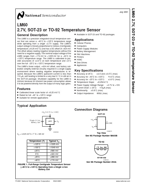
LM60CIZ
LM60CIZ Bulk
Accuracy Over Specified
Temperature Range ±3
±4
±3
±4
Specified Temperature
Range
−25˚C ≤ TA ≤ +125˚C
−40˚C ≤ TA ≤ +125˚C
−25˚C ≤ TA ≤ +125˚C
Human Body Model Machine Model
SOT-23 TO-92 Recommended Lead Temperature (Note 4): SOT Package: Vapor Phase (60 sec) Infrared (15 sec) TO-92 Package (3 sec, dwell time)
n Accuracy at 25˚C: ±2.0 and ±3.0˚C (max) n Accuracy for −40˚C to +125˚C: ±4.0˚C (max) n Accuracy for −25˚C to +125˚C: ±3.0˚C (max) n Temperature Slope: +6.25mV/˚C n Power Supply Voltage Range: +2.7V to +10V n Current Drain @ 25˚C: 110µA (max) n Nonlinearity: ±0.8˚C (max) n Output Impedance: 800Ω (max)
Note 2: When the input voltage (VI) at any pin exceeds power supplies (VI < GND or VI > +VS), the current at that pin should be limited to 5 mA.
CMT60N03中文资料

PIN CONFIGURATION
TO-252 TO-263
SYMBOL
D
Front View
Front View
D
SOURCE
DRAIN
GATE
G
1 2 3
S
G
1 2 3
S
N-Channel MOSFET
ABSOLUTE MAXIMUM RATINGS
Rating Drain to Source Voltage (Note 1) Drain to Current ¡Ð ¡Ð ¡Ð Continuous Tc = 25¢J , VGS@10V (Note 2) Continuous Tc = 100¢J , VGS@10V (Note 2) Pulsed Tc = 25¢J , VGS@10V (Note 3) Continue Symbol VDSS ID ID IDM VGS PD dv/dt TJ, TSTG EAS TL TPKG IAS Value 30 50 Fig.3 Fig.6 ±20 52 0.5 3.0 -55 to 150 500 300 260 Fig.8 V W W/¢J V/ns ¢J mJ ¢J ¢J Unit V A
Gate-to-Source Voltage ¡Ð Total Power Dissipation
Derating Factor above 25¢J Peak Diode Recovery dv/dt (Note 4) Operating Junction and Storage Temperature Range Single Pulse Avalanche Energy L=1.1mH,ID=30 Amps Maximum Lead Temperature for Soldering Purposes Maximum Package Body for 10 seconds Pulsed Avalanche Rating
3相6平方线表示方法

3相6平方线表示方法English:3-phase 6-wire systems are typically used in industrial and commercial settings where heavy machinery or large electrical loads are required. In a 3-phase 6-wire system, there are three hot, or current-carrying, conductors and three neutral conductors. The three hot conductors are connected to the three-phase power supply, while the neutral conductors are used to provide a return path for the current. The 6-wire system allows for a higher power capacity and greater stability compared to single-phase systems. This configuration also allows for the use of 3-phase motors and other equipment that require 3-phase power. Each hot conductor in the 3-phase system carries a current that is 120 degrees out of phase with the other two conductors, providing a more balanced and efficient power distribution.中文翻译:3相6平方线系统通常用于工业和商业环境,在这些地方通常需要大型的机械设备或大电力负载。
FSP350-60THN资料

• Complied with ATX12V 2.0 standard • High efficiency and reliability • Remote On/Off function • Internal 12V DC fan included • Noise Killer (Thermal fan speed control function) • Low noise and ripple • Complies with FCC part 15 subpart J Class B and CISPR 22
Class B • Output over voltage, short circuit, and over current protection • 100% Hi-pot, ATE, and burn-in tested • Re-settable power shut down • Approved by UL 60950, CSA C22.2 Level 3, TUV EN60950,
Specification
• Temperature Range: Operating 0° C ~ +25° C on full load; De-rate 2W/C from +50° C to +25° C; storage & shipping -20° C ~ +65° C
• Humidity: 90% on operating and 95% on storage • Dielectric Withstand: Input to frame ground 1800V AC
for 1 second • Efficiency: 70% at minimum measured at nominal AC
- 1、下载文档前请自行甄别文档内容的完整性,平台不提供额外的编辑、内容补充、找答案等附加服务。
- 2、"仅部分预览"的文档,不可在线预览部分如存在完整性等问题,可反馈申请退款(可完整预览的文档不适用该条件!)。
- 3、如文档侵犯您的权益,请联系客服反馈,我们会尽快为您处理(人工客服工作时间:9:00-18:30)。
1/9May 2000STP3NC60STP3NC60FPN-CHANNEL 600V -3.3Ω -3A TO-220/TO-220FPPowerMesh ™II MOSFETs TYPICAL R DS (on)=3.3Ωs EXTREMELY HIGH dv/dt CAPABILITY s 100%AVALANCHE TESTEDs NEW HIGH VOLTAGE BENCHMARK sGATE CHARGE MINIMIZEDDESCRIPTIONThe PowerMESH ™II is the evolution of the first generation of MESH OVERLAY ™.The layout re-finements introduced greatly improve the Ron*area figure of merit while keeping the device at the lead-ing edge for what concerns swithing speed,gate charge and ruggedness.APPLICATIONSs HIGH CURRENT,HIGH SPEED SWITCHING s SWITH MODE POWER SUPPLIES (SMPS)s DC-AC CONVERTERS FOR WELDING EQUIPMENT AND UNINTERRUPTIBLE POWER SUPPLIES AND MOTOR DRIVERABSOLUTE MAXIMUM RATINGS(•)Pulse width limited by safe operating areaTYPE V DSS R DS(on)I D STP3NC60600V <3.6Ω3A STP3NC60FP600V<3.6Ω2ASymbol ParameterValueUnit STP3NC60STP3NC60FPV DS Drain-source Voltage (V GS =0)600V V DGR Drain-gate Voltage (R GS =20k Ω)600V V GS Gate-source Voltage±30V I D Drain Current (continuos)at T C =25°C 33A I D Drain Current (continuos)at T C =100°C 1.9 1.9(*)A I DM (q )Drain Current (pulsed)1212(*)A P TOT Total Dissipation at T C =25°C 8040W Derating Factor0.640.32W/°C dv/dt (1)Peak Diode Recovery voltage slope 3.5V/ns V ISO Insulation Withstand Voltage (DC)-2000T stg Storage Temperature–60to 150°C T jMax.Operating Junction Temperature150°C(1)I SD ≤3A,di/dt ≤100A/µs,V DD ≤V (BR)DSS ,T j ≤T JMAX.(*)Limited only by maximum temperature allowedINTERNAL SCHEMATIC DIAGRAM123123TO-220TO-220FPSTP3NC60/FP2/9THERMAL DATAAVALANCHE CHARACTERISTICSELECTRICAL CHARACTERISTICS (TCASE =25°C UNLESS OTHERWISE SPECIFIED)OFFON (1)DYNAMICTO-220TO-220FP Rthj-case Thermal Resistance Junction-case Max 1.563.12°C/W Rthj-amb Thermal Resistance Junction-ambient Max 62.5°C/W Rthc-sinkThermal Resistance Case-sink Typ0.5°C/W T lMaximum Lead Temperature For Soldering Purpose300°CSymbol ParameterMax ValueUnit I AR Avalanche Current,Repetitive or Not-Repetitive (pulse width limited by T j max)3A E ASSingle Pulse Avalanche Energy(starting T j =25°C,I D =I AR ,V DD =50V)100mJSymbol ParameterTest ConditionsMin.Typ.Max.Unit V (BR)DSS Drain-sourceBreakdown Voltage I D =250µA,V GS =0600V I DSS Zero Gate VoltageDrain Current (V GS =0)V DS =Max Rating1µA V DS =Max Rating,T C =125°C 50µA I GSSGate-body Leakage Current (V DS =0)V GS =±30V±100nASymbol ParameterTest ConditionsMin.Typ.Max.Unit V GS(th)Gate Threshold Voltage V DS =V GS ,I D =250µA 234V R DS(on)Static Drain-source On ResistanceV GS =10V,I D =1.5A 3.33.6ΩI D(on)On State Drain CurrentV DS >I D(on)x R DS(on)max,V GS =10V3ASymbol ParameterTest ConditionsMin.Typ.Max.Unit g fs (1)Forward Transconductance V DS >I D(on)x R DS(on)max,I D =1.5A2S C iss Input Capacitance V DS =25V,f =1MHz,V GS =0400pF C oss Output Capacitance 57pF C rssReverse Transfer Capacitance7pF3/9STP3NC60/FPELECTRICAL CHARACTERISTICS (CONTINUED)SWITCHING ONSWITCHING OFFSOURCE DRAIN DIODENote: 1.Pulsed:Pulse duration =300µs,duty cycle 1.5%.2.Pulse width limited by safe operating area.Symbol ParameterTest ConditionsMin.Typ.Max.Unit t d(on)Turn-on Delay Time Rise Time V DD =300V,I D =1.5A R G =4.7ΩV GS =10V (see test circuit,Figure 3)9ns t r 13ns Q g Total Gate Charge V DD =480V,I D =3A,V GS =10V1318.2nC Q gs Gate-Source Charge 2.3nC Q gdGate-Drain Charge4.4nCSymbol ParameterTest ConditionsMin.Typ.Max.Unit t r(Voff)Off-voltage Rise TimeV DD =480V,I D =3A,R G =4.7Ω,V GS =10V (see test circuit,Figure 5)13ns t f Fall Time 15ns t cCross-over Time21nsSymbol ParameterTest ConditionsMin.Typ.Max.Unit I SD Source-drain Current 3A I SDM (2)Source-drain Current (pulsed)12A V SD (1)Forward On Voltage I SD =3A,V GS =01.6V t rr Reverse Recovery Time I SD =3A,di/dt =100A/µs,V DD =100V,T j =150°C(see test circuit,Figure 5)420ns Q rr Reverse Recovery Charge 1.5µC I RRMReverse Recovery Current7.1ASafe Operating Area for TO-220Safe Operating Area for TO-220FPSTP3NC60/FP4/9Static Drain-source On ResistanceThermal Impedence for TO-220 Output Characteristics Thermal Impedence for TO-220FP Transfer CharacteristicsTransconductanceSTP3NC60/FPNormalized Gate Threshold Voltage vs Temp. Source-drain Diode Forward Characteristics Capacitance VariationsNormalized On Resistance vs TemperatureGate Charge vs Gate-source Voltage5/9STP3NC60/FP6/9Fig.5:Test Circuit For Inductive Load Switching And Diode Recovery TimesFig.4:Gate Charge test CircuitFig.2:Unclamped Inductive WaveformFig.1:Unclamped Inductive Load Test CircuitFig.3:Switching Times Test Circuit For Resistive Load7/9STP3NC60/FPDIM.mminch MIN.TYP.MAX.MIN.TYP.MAX.A 4.40 4.600.1730.181C 1.23 1.320.0480.051D 2.402.720.0940.107D1 1.270.050E 0.490.700.0190.027F 0.610.880.0240.034F1 1.14 1.700.0440.067F2 1.14 1.700.0440.067G 4.95 5.150.1940.203G1 2.4 2.70.0940.106H210.010.400.3930.409L216.40.645L413.014.00.5110.551L5 2.65 2.950.1040.116L615.2515.750.6000.620L7 6.2 6.60.2440.260L9 3.5 3.930.1370.154DIA.3.75 3.850.1470.151L6ACDED 1FGL7L2Dia.F 1L5L4H 2L9F 2G 1TO-220MECHANICAL DATAP011CSTP3NC60/FP8/9DIM.mm inchMIN.TYP.MAX.MIN.TYP.MAX.A 4.4 4.60.1730.181B 2.5 2.70.0980.106 D 2.5 2.750.0980.108 E0.450.70.0170.027 F0.7510.0300.039 F1 1.15 1.70.0450.067 F2 1.15 1.70.0450.067 G 4.95 5.20.1950.204 G1 2.4 2.70.0940.106 H1010.40.3930.409 L2160.630L328.630.6 1.126 1.204 L49.810.60.3850.417 L615.916.40.6260.645 L799.30.3540.366Ø3 3.20.1180.126L2ABDEH GL6¯FL3G1123F2F1L7L4TO-220FP MECHANICAL DATASTP3NC60/FPInformation furnished is believed to be accurate and reliable.However,STMicroelectronics assumes no responsibility for the consequencesof use of such information nor for any infringement of patents or other rights of third parties which may result from its use.No license is granted by implication or otherwise under any patent or patent rights of STMicroelectronics.Specification mentioned in this publication aresubject to change without notice.This publication supersedes and replaces all information previously supplied.STMicroelectronics productsare not authorized for use as critical components in life support devices or systems without express written approval of STMicroelectronics.The ST logo is a trademark of STMicroelectronics©2000STMicroelectro nics–Printed in Italy–All Rights ReservedSTMicroelectronics GROUP OF COMPANIESAustralia-Brazil-China-Finland-France-Germany-Hong Kong-India-Italy-Japan-Malaysia-Malta-Morocco-Singapore-Spain-Sweden-Switzerland-United Kingdom-U.S.A.9/9。
