Digital Logic Tutorial and Design - Keith E Holbert数字逻辑设计教程与基思E霍尔伯特22页
数字逻辑设计Digital Logic Design.pdf
数字逻辑设计——绪论
13
数字的出现
数字的出现
数字在各个古代文明中都独立的存在 数字都采用十进制数 阿拉伯数字
Digit的词义
人的手指或脚趾 指宽 阿拉伯数字符号从0到9中的任意一个 用于计算系统中的符号
数字逻辑设计——绪论
14
早期的计算用具
数字逻辑设计——绪论
11
构造计算机的装置
电子装置
处理器 存储器
机械装置
用于磁盘读写的寻道手臂
光学装置
CDROM
数字逻辑设计——绪论
12
计算的历史
计算机历史只有50年多年?
不对! 数字电子计算机的历史只有50多年! 计算机革命发生在过去的50多年中而且还正在进行
计算和计算机的历史源远流长…… 把握历史
数字逻辑设计——绪论
17
二进制的早期应用
1844 Samuel Morse 电报
编码和解码
航海信号灯
信号灯的开和关表示信息
1876 Alexander Bell 电话
AT&T公司 电话开关网络的发展 继电器(relay)的应用
数字逻辑设计——绪论
18
继电器(机电计算机)
Konrad Zuse’s Z-1 (1935) 1937,Howard Aiken Model-K 1937,George Slibitz of Bell Laboratory
数字逻辑设计——绪论
27
Moore 定律
Dr. Gordon E. Moore is Chairman Emeritus of Intel Corporation. He co-founded Intel in 1968, serving initially as Executive Vice President. He became President and Chief Executive Officer in 1975 and held that post until being elected Chairman and Chief Executive Officer in 1979. He remained CEO until 1987 and served as Chairman until being named Chairman Emeritus in 1997.
软硬件结合的书籍

软硬件结合的书籍
1. 《数字逻辑与计算机设计》(Digital Logic and Computer Design) by M. Morris Mano - 这本书是计算机系统结构和数字逻辑的经典教材,非常适合初学者。
2. 《计算机组成与设计:硬件/软件接口》(Computer Organization and Design: The Hardware/Software Interface) by David A. Patterson and John L. Hennessy - 这本书是现代计算机体系结构的经典教材,介绍了计算机硬件和软件之间的接口。
3. 《操作系统设计与实现》(Operating System Concepts) by Abraham Silberschatz, Peter B. Galvin, and Greg Gagne - 这本书详细介绍了操作系统的设计和实现原理,涵盖了软硬件交互的多个方面。
4. 《嵌入式系统设计与开发》(Embedded Systems: Design and Development) by Daniel W. Lewis - 这本书介绍了嵌入式系统的设计和开发原理,包括硬件、软件和系统集成等方面的内容。
5. 《计算机体系结构:量化方法》(Computer Architecture: A Quantitative Approach) by John L. Hennessy and David A. Patterson - 这本书以量化方法为基础介绍了计算机体系结构的各个方面,强调软硬件结合的设计和优化。
这些书籍适合对软硬件结合有兴趣的读者,无论是初学者还是有一定计算机基础的读者都可以从中获得有用的知识。
计算机组成与设计英文版第四版课程设计 (2)

Course Design for Computer Organization and Design4th EditionIntroductionThe course design for Computer Organization and Design (COD) 4th edition is designed to provide students with an understanding of the fundamental principles of computer organization and design. The course is divided into three mn units: the first unit covers the basic principles of digital logic and circuit design, the second unit covers the architecture and organization of computer systems, and the third unit covers advanced topics such as parallel processing and memory hierarchies.Course ObjectivesUpon completion of the course, students will be able to: - Understand the basic principles of digital logic and circuit design, including boolean algebra, gates, and flip-flops - Understand the architecture and organization of basic computer systems, including the CPU, memory, and I/O devices - Design and implement basic digital circuits using logic gates and flip-flops - Understand the purpose and function of assembly language and machine language, including instruction sets, memory addressing modes, and CPU operations - Understand the basic principles of pipelining and parallel processing, including pipelined CPU design and parallel processing architectures - Understand the principles of memory hierarchies and caching, including the function and organization of cache memoryCourse Outline•Unit 1: Digital Logic and Circuit Design–Introduction to digital logic–Boolean algebra and logic gates–Flip-flops and sequential circuits–Design of basic digital circuits•Unit 2: Computer System Organization and Architecture–Introduction to computer system organization–CPU organization and instruction sets–Memory organization and addressing modes–Input/output (I/O) devices and interfaces–Assembly language programming and machine language •Unit 3: Advanced Topics in Computer Organization and Design –Pipelining and parallel processing–Cache memory and memory hierarchies–Advanced CPU design and architectures–High-performance computer systemsCourse Delivery and AssessmentThe course will be delivered through a combination of lectures, tutorials, and laboratory work. There will be a mid-term exam and afinal exam as well as regular assessments throughout the course. The lab work will be designed to provide hands-on experience with digitalcircuit design, CPU design, and assembly language programming.ConclusionThe design of the COD 4th edition course is intended to provide a strong foundation in the principles of computer organization and design. By the end of the course, students will have gned the skills necessary to design and implement basic digital circuits and understand the architecture and organization of computer systems. With the rapid changes and developments in computer hardware, it is essential for students to have a solid understanding of the fundamental principles underlying computer systems.。
介绍计算机组成原理这门学科的英语作文

介绍计算机组成原理这门学科的英语作文Computer organization and design is a fundamental subject in the field of computer science. 计算机组成原理和设计是计算机科学领域的一门基础课程。
It focuses on the understanding and design of computer systems at the hardware level, and plays a crucial role in shaping the way modern computing systems work. 它关注的是在硬件层面上理解和设计计算机系统,并且在塑造现代计算系统的工作方式上起着至关重要的作用。
At its core, computer organization and design delves into the architecture and functionality of computer hardware components such as the CPU, memory, and I/O devices. 在其核心,计算机组成原理和设计深入研究了计算机硬件组件的体系结构和功能,如CPU、内存和I/O 设备。
It aims to provide a comprehensive understanding of how these components work together to execute instructions, process data, and perform various computational tasks. 它旨在提供对这些组件如何一起执行指令、处理数据和执行各种计算任务的全面理解。
Furthermore, the study of computer organization and design often involves exploring the principles of digital logic and circuit design. 此外,计算机组成原理和设计的研究通常涉及探索数字逻辑和电路设计的原理。
数字逻辑设计VHDL基础英文版教学设计 (3)
Digital Logic Design VHDL Basics Teaching Design(English Version)IntroductionDigital logic design is the basis of modern computer engineering. It is a critical subject that introduces students to the fundamental concepts of digital circuits and computer architectures. To facilitate the learning of this subject, a teaching design that encompasses VHDL (VHSIC Hardware Description Language) will be outlined in this article. The design will cover the essential concepts, such as combinational and sequential logic, and it will utilize VHDL to illustrate how digital systems can be described and simulated in a digital design environment.ObjectivesThe primary objective of this teaching design is to introduce students to digital logic design and VHDL. The following objectives will be achieved:1.Students will understand digital circuits and theircomponents, such as logic gates and flip-flops.2.Students will grasp the basic concepts of combinational andsequential circuits.3.Students will learn the fundamentals of VHDL and its role indigital circuit design.Pre-requisitesThe following pre-requisites are assumed for students undertaking this course:1.High school level mathematics and physics.2.Basic understanding of digital circuits and binary numberingsystems.Course OutlineThis course is divided into two parts: Theory and VHDL. The theory part provides students with a fundamental understanding of digital circuits and their properties, while the VHDL section instructs students on how to describe digital circuits.Part 1: TheoryTopic 1: Digital Circuit Fundamentals•Definition of Digital Circuits•Numbering Systems•Logic Gates•Combinational Circuits•Flip-FlopsTopic 2: Combinational Circuits•Introduction to Combinational Circuits•Truth Tables•Boolean Algebra•Karnaugh Maps•Implementation of Combinational CircuitsTopic 3: Sequential Circuits•Introduction to Sequential Circuits•Flip-flops•Registers•CountersPart 2: VHDLTopic 4: VHDL Overview•VHDL Overview•Signals•Types•Operators•Concurrent and Sequential Statements Topic 5: Combinational Circuit Design in VHDL •VHDL Combinational Circuits•Signal Assignment•Process Statements•Behavioural Modelling•Structural ModellingTopic 6: Sequential Circuit Design in VHDL •Sequential Circuit Design•Process Statements•Concurrent signal Assignment•ARROW Operator•Timing ConstrntsAssessment GuidelinesThe following guidelines will be used to assess student’s performance in this course:1.Assignments (60%) - Students will be required to completeassignments covering both the theory and the VHDL sections of the course.boratory Work (20%) - Students will be required todemonstrate the skills learned in the VHDL section of the courseby designing and simulating digital circuits in a digital designenvironment.3.Final Exam (20%) - A final exam covering both the Theory andVHDL sections of the course will be conducted.ConclusionDigital Logic Design and VHDL are essential components of modern computer engineering. The teaching design outlined in this article ms to provide a fundamental understanding of digital circuits as well as VHDL and its role in digital circuit design. Students who successfully complete this course will be well equipped with the skills and knowledge required to design digital circuits and simulate them in a digital design environment.。
电子科大 数字电路 最好老师的课件第一章

Flip-flops(触发器): (触发器):
—— A device that stores either 0 or 1 (一种能存储 0 或 1 的器件 一种能存储 的器件) P7 Figure 1-1
12
Digital Logic Design and Application (数字逻辑设计及应用 数字逻辑设计及应用) 数字逻辑设计及应用
5
3次 次 3次 次 11次 次 2次 次 11次 次 1次 次 1次 次
引言, 引言,数制与编码 数字电路器件基础 组合电路分析与设计 Verilog语言 语言 时序电路分析与设计 存储器和可编程器件 DAC和ADC 和
Digital Logic Design and Application (数字逻辑设计及应用) 数字逻辑设计及应用)
1.2 Analog versus Digital 模拟与数字) (模拟与数字) Digital Circuits over Analog Ones (数字系统及其优越性)
Reproducibility of Results [结果再现性(稳定可靠、精度更高)] 结果再现性( 结果再现性 稳定可靠、精度更高) Ease of design, Flexibility, and Functionality (易于设计,灵活性和功能性 易于设计, 易于设计 灵活性和功能性) Programmability [可编程性(HDL 硬件描述语言)] 可编程性( 硬件描述语言) 可编程性 Speed, Economy, and Steadily Advancing Technology (快速、经济性、稳步发展的技术 快速、 快速 经济性、稳步发展的技术)
2
Digital Logic Design and Application (数字逻辑设计及应用) 数字逻辑设计及应用) 课程安排: 学时 课程安排:64学时 教材: 教材: 数字设计—原理与实践 原理与实践( 数字设计 原理与实践(第4版 影印版) 版 影印版) John F. Wakerly 高等教育出版社 2007 参考书: 参考书: 1.数字逻辑设计及应用 姜书艳主编, 1.数字逻辑设计及应用,姜书艳主编,清华大学出版 数字逻辑设计及应用, 社,2007 2. 数字电子技术基础 (第5版),阎石主编,高等教 阎石主编, 版),阎石主编 育出版社, 育出版社,2007 3. 数字设计 原理与实践(第4版), 数字设计—原理与实践 原理与实践( 版),John F. Wakerly, , 林生 等译,机械工业出版社,2007 等译,机械工业出版社, 4. 数字电路与系统 (第2版),刘宝琴等编著,清华大学 刘宝琴等编著, 版),刘宝琴等编著 出版社,2007 出版社, 5. 数字电路逻辑设计(第3版),王毓银主编,高等教育 数字电路逻辑设计( 王毓银主编, 版),王毓银主编 出版社, 出版社,2006
使用multisim进行数字逻辑电路建模与仿真说明书
DIGITAL LOGIC CIRCUIT MODELING AND SIMULATION WITH MULTISIMMultisim is a schematic capture and simulation program for analog, digital and mixed analog/digital circuits, and is one component of the National Instruments “Circuit Design Suite”.The basic steps in modeling and analysis of a digital logic circuit are:1.Open Multisim and create a “design”.2.Draw a schematic diagram of the circuit (components and interconnections).3.Design digital test patterns to be applied to the circuit inputs to stimulate the circuit and connect signal sourcesto the circuit inputs to produce these patterns.4.Connect the circuit outputs to one or more indicators to display the response of the circuit to the test patterns.5.Run the simulation and examine the results, copying and pasting Multisim windows into lab reports and otherdocuments as needed.6.Save the design.Step 1. Open Multisim and create a designThis creates a blank design called “Design1”, as illustrated in Figure 1. Save the file with the desired design name via menu bar File>Save As to use the standard Windows Save dialog.A previously saved design can be opened via File>Open. In the dialog window, navigate to the directory in which the design is stored, select the file, and click the Open button.Figure 1. Blank design with default name “Design 1.”Step 2. Draw a schematic diagram of the circuitPlace ComponentsA schematic diagram comprises one or more circuit components, interconnected by wires. Optionally, signal “sources” may be connected to the circuit inputs, and “indicators” to the circuit outputs. Each component is selected from the Multisim library and placed on the drawing sheet in the Circuit Window (also called the Workspace). The Multisim library is organized into “groups” of related components (Transistors, Diodes, Misc Digital, TTL, etc.). Each group comprises one or more “families”, within which the components are implemented with a common technology. For designing and simulating digital logic circuits in this course, “Misc Digital” (TIL family only) is used.The “Misc Digital” group has three families of components, of which family “TIL” contains models of generic logic gates, flip-flops, and modular functions. These components are technology-independent, which means that they have only nominal circuit delays and power dissipation, unrelated to any particular technology. Generic components can be used to test the basic functionality of a design, whereas realistic timing information requires the use of technology-specific part models, such as those in the TTL group.To place a component on the drawing sheet, select it via the Component Browser, which is opened via the component toolbar or the menu bar. From the menu bar, select Place>Component to open the Component Browser window, illustrated in Figure 2. You can also open this window by clicking on the Misc Digital icon in the component toolbar. On the left side of the window, select “Master Database”, group “Misc Digital”, and family “TIL”. The component panel in the center lists all components in the selected family. Scroll down to and click on the desired gate (NAND2 Figure 3); its symbol and description are displayed on the right side of the window. Then click the OK button. The selected gate will be shown on the drawing sheet next to the cursor; move the cursor to position the gate at the desired location, and then click to fix the position of the component. The component can later be moved to a different location, deleted, rotated, etc. by right clicking on the component and selecting the desired action. You may also select these operations via the menu bar Edit menu.Figure 2. Component Browser: Misc Digital TIL family NAND2 gate component selected.Figure 3. A third NAND2 gate is about to be placed on the drawing sheet.Figure 4 shows the schematic diagram with four placed components. Note that each placed gate has a “designator” (U2, U3, U4, U5), which can be used when referring to that gate. You can change a designator by right clicking on the component, selecting Properties, and entering the desired name on the Label tab.Figure 4. Schematic diagram with all placed components.Drawing WiresWires are drawn between component pins to interconnect them. Moving the cursor over a component pin changes the pointer to a crosshair, at which time you may click to initiate a wire from that pin. This causes a wire to appear, connected to the pin and the cursor. Move the cursor to the corresponding pin of the second component (the wire follows the cursor) and click to terminate the wire on that pin. If you do not like the path selected for the wire, you may click at a point on the drawing sheet to fix the wire to that point and then you can move the cursor to continue the wire from that point. You may also initiate or terminate a wire by clicking in the middle of a wire segment, creating a “junction” at that point. This is necessary when a wire is to be fanned out to more than one component input. A partially-wired circuit, including one junction point, is illustrated in Figure 5.Figure 5. Partially wired circuit, with one junction point.Step 3. Generating test input patterns.To drive circuit simulations, Multisim provides several types of “sources” and “instruments” to generate and apply patterns of logic values to digital circuit inputs. Sources are placed on the schematic sheet and connected to circuit inputs in the same way as circuit components, selecting them from the “Digital_Sources” family of the “Sources” group in the component browser. Note that there is a Place Source shortcut icon in the tool bar.There are three basic digital sources:1.DIGITAL_CONSTANT – this is a box with a constant logic 1 or 0 output, and would be used where the logic valueis not to be changed during simulation. To change the output value, right click on the box, select Properties, select the desired value on the Value tab, and click the OK button.2.INTERACTIVE_DIGITAL_CONSTANT – this is a clickable box that can be connected to a circuit input. Clicking onthe box toggles its output between 0 and 1. This can be used to interactively change a circuit input duringsimulation.3.DIGITAL_CLOCK – this is a box that produces a repeating pulse train (square waveform), oscillating between 0and 1 at a specified frequency. To set the frequency and duty cycle, right click on the box, select Properties,select the desired frequency and duty cycle value on the Value tab, and click the OK button.Figure 6 shows the circuit of Figure 5 with an INTERACTIVE_DIGITAL_CONSTANT connected to each input. Note that the initial state of each is logic 0. Since this circuit has only three inputs, all 8 input patterns can be produced (to generate a truth table for the circuit) by manually toggling the inputs.Figure 6. INTERACTIVE_DIGITAL_CONSTANT sources connected to circuit inputs.Step 4. Connect circuit outputs to indicatorsTo facilitate studying the digital circuit output(s), Multisim provides a variety of “indicators”. For digital simulation, the most useful are digital “probes”, hex displays, and the Logic Analyzer instrument. A probe, illustrated in Figure 7, displays a single digital value as ON or OFF (the probe is “illuminated” indicating an ON condition). The PROBE family of the Indicators group includes a generic PROBE_DIG and several PROBE_DIG_color indicators (color = BLUE, GREEN, ORANGE, RED, YELLOW). The probe in Figure 7 is PROBE_DIG_BLUE. This circuit can be verified by manually changing the three INTERACTIVE_DIGITAL_CONSTANT inputs to each of the 8 possible combinations, and recording the probe value for each combination to create a truth table.Figure 7. DIGITAL_PROBE_BLUE connected to circuit output.Step 5. Run the simulationA simulation is initiated by pressing the Run (green arrow) button in the toolbar or via the menu bar via Simulate>Run. You may simulate the circuit by clicking on the keys to change the input values and observe the output changes through the LED indicator.You may capture any window and paste it into a Word or other document for generating reports. An individual window is captured by pressing the ALT and Print Screen keys concurrently. You may then “paste” the captured window into a document via the editing features of that document. To capture a circuit diagram in the main window, the simplest method is via the menu bar Tools>Capture Screen Area. This produces a rectangle whose corners can be stretched to include the screen area to be captured; the “copy” icon on the top left corner is pressed to copy the area, which may then be pasted into a document.Step 6. Save the design and close MultisimThe simplest way to save a design is to click the Save icon in the Design Toolbar on the left side of the window, directly above the design name. Alternatively, you may use the standard menu bar File>Save.Multisim is exited as any other Windows program.-This document is a modified and short version of /department/ee/elec2210/.Appendix: Creating subcircuits and hierarchical blocks (from NI Multisim manual)Complete the following steps to place a new subcircuit:1. Select Place»New subcircuit. The Subcircuit Name dialog box appears.2. Enter the name you wish to use for the subcircuit, for example, “PowerSupply” andclick OK. Your cursor changes to a “ghost” image of the subcircuit indicating that thesubcircuit is ready to be placed.3. Click in the desired location to place the subcircuit.4. Double-click on the new subcircuit and select Open subsheet from the Label tab ofthe Hierarchical Block/Subcircuit dialog box that displays. An empty design sheetappears.5. Place and wire components as desired in the new subcircuit.6. Select Place»Connectors»Hierarchical connector, and place and wire the connector asdesired. Repeat for all required hierarchical connectors.When you attach a hierarchical connector to a wire, the net name for the wire that you connect it to does not change if it has a Preferred net name (user-assigned via the NetProperties dialog box). If the net name on the wire is auto-named, it changes to match theconnector.7. Select the sheet that contains the subcircuit from the Hierarchy tab of the DesignToolbox.OrSelect View»Parent sheet.This command moves you up to the next sheet in the hierarchy. If you have multiple nested circuits and are viewing, for example, a subcircuit within a subcircuit, you will notmove to the top of the hierarchy.The symbol for the subcircuit that appears includes pins for the number of connectors thatyou added.8. Wire the hierarchical connectors into the main circuit.Complete the following steps to place another instance of the same subcircuit:1. Select the desired subcircuit and select Edit»Copy.2. Select Edit»Paste to place a copy of the subcircuit on the workspace.。
数字逻辑设计VHDL基础英文版教学设计 (2)

Introduction to VHDL Basic in Digital Logic DesignTeachingDigital logic design is one of the most critical concepts in modern electronics and computer science, and its importance continues to risein the ever-increasing complexity of modern technology. Undoubtedly, the field of digital logic design is constantly evolving in terms of hardware and software and providing solutions for various industries’ needs and requirements. In line with this, VHDL (VHSIC Hardware Description Language) has emerged as the standard language for digital circuit design and is widely used in problem-solving.The primary emphasis of this document is to get acqunted with VHDL basic concepts and its implementation in digital logic design. The document starts by providing an overview of the fundamentals of VHDL and then continues with its implementation techniques.Overview of VHDLVHDL is a text-based language used in the description of digital circuitry, particularly FPGA (Field Programmable Gate Array) designs, ASICs (Application-Specific Integrated Circuits), and other digital circuits. The primary purpose of VHDL is to represent the behavior, structure, and explicit interconnection of the circuit. Moreover, VHDLis used for verification, synthesis, and testing of digital circuits.The VHDL language has a hierarchical structure to organize the design. It is divided into entities and architectures, and the implementation of designs is accomplished using models. The entitiesrepresent the circuit’s external interface and define the inputs and outputs, as well as their data types. The architectures describe the components’ internal workings, and different architectures can be created for an entity.VHDL Implementation TechniquesThe most common implementation techniques used in VHDL digital logic design are behavioral, data flow, and structural description.Behavioral DescriptionBehavioral description involves creating an algorithm that reflects the intended design’s behavior. The algorithm is described in high-level programming languages, such as C or Java, and translated into VHDL code. Behavioral modeling is beneficial as designers can verify the circuit’s behavior before synthesizing the code and implementing the design in hardware.Data Flow DescriptionData flow description forms a direct connection of data flow between a signal input and a signal output. It is based on the flow of data in the design and is helpful in the optimization of speed and area. In data flow modeling, the circuit’s functionality is described by a set of interconnected processes that exchange signals through signals and variables.Structural DescriptionStructural description involves describing the circuit’s components by the sub-circuits that comprise the design’s full structure. Instructural design, the design is divided into several subsystems, each implementing a particular functionality. The subsystems are concatenated to form the final design. Structural modeling is helpful in incremental design development, where subsystems can be modeled and tested separately.ConclusionIn conclusion, VHDL is a necessary tool for digital circuit design and is widely used by engineers worldwide. VHDL’s ability to describe the structure, behavior, and explicit connection of circuits makes it a powerful tool in the world of digital logic design. The implementation techniques discussed in this document are behavioral, data flow, and structural description. Each technique has specific advantages and disadvantages, and selecting an appropriate implementation method depend s on the design’s complexity and requirements.As educators, it is essential to provide students with an understanding of basic VHDL concepts in digital logic design. With these VHDL foundations, students can subsequently explore advanced VHDL programming concepts and develop digital circuits on FPGA platforms and ASICs.。
第四章数字逻辑 (5)

Simplifying Products of Sums (简化“和之积”表达式)
AB CD
00 01 11 10
00
01
11
10
A’+C
0
0
0
0
0
0
0
0 Variable (原变量) 1 Complement of a Variable A’+B (反变量)
F = (A+B’+C’+D)·(A’+C)·(A’+B)
卡诺图的特点
10 2
6
14
10
相邻两方格只有一个因子互为反变量
合并最小项
2n个最小项相邻可消去n个因子
3
Digital Logic Design and Application (数字逻辑设计及应用)
化简:F = A,B,C,D ( 0, 2, 3, 5, 7, 8, 10, 11, 13 ) 1、填图
1
Digital Logic Design and Application (数字逻辑设计及应用)
Minimize Logic Function (化简逻辑函数)
什么是最简
公式法化简
项数最少
每项中的变量数最少
卡诺图表示逻辑函数
卡诺图化简
卡诺图的特点
合并最小项(化简)
Several Concepts (几 个 概 念)
质主蕴含项
(Essential Prime implicant ): 含有其他圈不含的最小项的 主蕴含项;
奇异1单元
(Distinguished 1-cell ): 只存在于一个质主蕴含项中的 1单元;
数字逻辑设计VHDL基础英文版课程设计 (2)

IntroductionThis document presents the design of a VHDL-based digital logic design course. The course is med to provide the learners with a basic understanding of digital logic design using VHDL. The mn objective of the course is to enable the learners to design digital circuits, simulate them, and implement them on FPGA devices.The course will cover basic digital logic design concepts, such as Boolean algebra, logic gates, combinational circuits, sequential circuits, and VHDL language. The course materials will be delivered in English, and the learners will have the opportunity to practice their skills through different design projects.Course ContentModule 1: Introduction to Digital Logic Design•Introduction to digital logic design•Digital systems and binary numbers•Boolean algebra and logic gates•Truth tables and Karnaugh maps•Combinational circuits and arithmetic circuits Module 2: Sequential Circuits•Introduction to sequential circuits•Flip-flops and latches•State diagrams and state tables•Design and implementation of synchronous and asynchronous sequential circuitsModule 3: VHDL Language•Introduction to VHDL language•VHDL data types and operators•VHDL architecture and entities•Writing and testing VHDL code•Simulation and synthesis of VHDL codeModule 4: Design ProjectsIn this module, the learners will work on different design projects using VHDL language. The projects will cover different aspects ofdigital logic design, such as:•Design and implementation of combinational circuits•Design and implementation of sequential circuits•Implementation of a microprocessor using VHDL•Design of a digital clock using VHDLLearning OutcomesUpon completion of this course, the learners will be able to: •Understand the basic concepts of digital logic design•Design, simulate, and implement digital circuits using VHDL•Analyze and troubleshoot digital circuits•Use simulation software to validate digital circuits•Work independently and in a team on digital logic design projects.ConclusionThe VHDL-based digital logic design course provides a comprehensive understanding of digital logic design using VHDL. The course med to enable the learners to design digital circuits, simulate them, and implement them on FPGA devices. The project-based approach of the course allows learners to apply their knowledge and practice their skills. The course learning outcomes would enable the learners to pursue further studies in the field of digital logic design and its applications.。
数字ic设计自学流程
数字ic设计自学流程Studying digital IC design on your own can be a challenging but rewarding endeavor. It requires dedication, patience, and perseverance to become proficient in this field. 通过自学数字ic设计可以让您在这个领域中变得更加精通,虽然这可能是一个具有挑战性但有益的努力。
One of the first steps in the self-learning process is to gain a good understanding of the basic concepts of digital IC design. This includes learning about logic gates, flip-flops, registers, and other fundamental building blocks of digital circuits. 在自学过程中的第一步是要对数字ic设计的基本概念有很好的理解。
这包括学习逻辑门、触发器、寄存器和其他数字电路的基本构建模块。
It is also essential to become familiar with the tools and software used in digital IC design, such as Verilog, VHDL, and Electronic Design Automation (EDA) tools. These tools are essential for designing, simulating, and testing digital circuits. 熟悉数字ic设计中使用的工具和软件也很重要,比如Verilog、VHDL和电子设计自动化工具。
数字逻辑设计VHDL基础英文版课程设计
VHDL Basics Course Design for Digital Logic Design IntroductionVHDL (VHSIC Hardware Description Language) is a programming language used to model digital circuits. It is widely used to design and verify digital systems, including integrated circuits, field-programmable gate arrays (FPGAs), and complex systems on a chip. The purpose of this course design is to provide a basic understanding of VHDL for digital logic designers, including syntax and design methodologies.Course OverviewCourse Objectives1.Understand the syntax of VHDL and how to use it for digitalcircuit design.2.Understand the design methodologies and best practices fordesigning digital circuits using VHDL.3.Design, simulate, and test digital circuits using VHDL.Course Outline•Introduction to VHDL–History and background of VHDL–VHDL basics–VHDL tools and simulators•VHDL language syntax–Data types and operations–Structural VHDL (entity and architecture)–Behavioral VHDL (processes and signals)–Package and library•Design methodologies–Design process–Design with hierarchy•VHDL simulation–Testbench design–Simulation basics–Debugging techniques•VHDL synthesis–Synthesis basics–Synthesis tools•FPGA implementation–Basics of FPGA architecture–Implementing VHDL on FPGAsTeaching MethodsThe course will be delivered through a combination of lectures, discussions, and hands-on exercises. Each topic will be briefly explned in a lecture, followed by discussion to clarify any doubts or questions. Finally, students will brnstorm and implement a small project to apply the concepts learned in the lecture.Materials needed•Access to a VHDL compiler and simulator, such as ModelSim or Xilinx ISE•Access to a FPGA development boardCourse DesignTarget AudienceThe course is designed for undergraduate and graduate students of electronics and computer science engineering who have a basic understanding of digital logic design. It is also suitable for working professionals who are interested in digital circuit design using VHDL.Course DurationThe course will be conducted for a duration of 10 weeks, with one class of three hours per week.Course Assessment•Midterm examination (30%)•Final examination (50%)•Implementation project (20%)ConclusionThe VHDL basics course design will provide students with a strong foundation in VHDL, enabling them to design, simulate, and test digital circuits using VHDL. With the increasing demand for digital circuit designers in industry, this course will equip students with valuable skill sets and knowledge that can be effectively used in their professional careers.。
数字技术助力设计流程简约

数字技术助力设计流程简约【中英文版】英文文档:Digital technology has revolutionized the design process, making it more streamlined and efficient.With the help of various digital tools and software, designers can now create, collaborate, and communicate more effectively, leading to a simpler and more organized workflow.One of the key benefits of digital technology in design is the ability to work with digital files.These files can be easily edited, shared, and stored, eliminating the need for physical copies and reducing the risk of errors and loss.Designers can also work on projects simultaneously, regardless of their location, thanks to cloud-based collaboration tools.Furthermore, digital technology has enabled the automation of repetitive tasks, such as rendering and modeling, allowing designers to focus on more creative aspects of their work.With the help of AI and machine learning algorithms, designers can also receive valuable feedback and suggestions, improving the quality of their designs.In addition, digital technology has made it easier for designers to communicate with clients and stakeholders.Through various digital platforms, designers can showcase their work, gather feedback, and make necessary revisions in a timely manner.Overall, digital technology has significantly simplified the designprocess, enabling designers to work more efficiently and effectively.As technology continues to advance, it is exciting to imagine the possibilities it will bring to the design industry in the future.中文文档:数字技术已经彻底改变了设计流程,使其更加简洁高效。
数位积体电路雏型制作
05
多重設計模型---Area & Speed的考量
06
序向邏輯設計法
07
ASM與有限狀態機
08
ASM+Data path
09
乒乓球遊戲機設計實務
10
多重有限狀態機co-design
Kun Shan University
教學內容
11
系統分割Partition
12
Top Down/Button Up
教學大綱
數位積
科目名稱(中文)
體電路 雛型製
科目代碼
作
CK 13 授課部別 50
二 技
授課班級
CK032 電子三 B
Digital Circuit 科目名稱(英文) Protot 學分數 ype Design
3 上課總時數 3 授課教師 蔡國瑞
科目類別 教學目標
校訂必 修科目
修課別
必
修 課
實習時數
程
0
授課地點
FPGA實 驗室
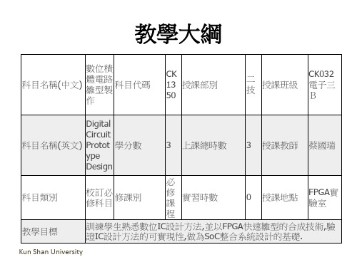
訓練學生熟悉數位IC設計方法,並以FPGA快速雛型的合成技術,驗 證IC設計方法的可實現性,做為SoC整合系統設計的基礎.
Kun Shan University
教學內容
01
ASIC設計概述
02
VHDL語法與ISE7.1設計環境
03
ISE7.1設計環境實務演練
04
組合邏輯設計法
13
智慧型遊戲機設計實務
14
遞迴與數學
15
multi-byte加減法器設計與pipeline
16
乘法器與除法器
17
簡易RISC微控制器設計
Shan University
基本数字电子概念与技巧教程说明书
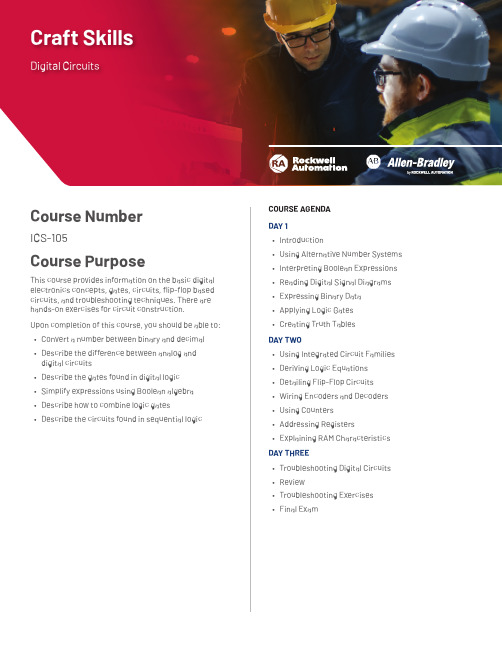
Course NumberICS-105Course PurposeThis course provides information on the basic digital electronics concepts, gates, circuits, flip-flop based circuits, and troubleshooting techniques. There are COURSE AGENDADAY 1• Introduction• Using Alternative Number Systems • Interpreting Boolean Expressions • Reading Digital Signal Diagrams • Expressing Binary DataCraft Skills Digital CircuitsWHO SHOULD ATTENDThis course is designed for electrical maintenance technicians, electronic technicians or I&C technicians.PREREQUISITESTo successfully complete this course, the following prerequisites are required:• Understanding of electrical theory and electrical systems STUDENT MATERIALSTo enhance and facilitate the students’ learningexperiences, the following materials are provided as part of the course package:• Student Manual– Includes the key concepts, definitions, examples, and activities presented in this course • Lab Guide which includes the hands-on exercisesHANDS-ON PRACTICEThroughout this course, you will have the opportunity to practice the skills you have learned through a variety of hands-on exercises. These exercises focus on the skills introduced in each lesson.You will also have the opportunity to combine and practice groups of key skills by completing multiple integrated practices during the course.NEXT LEARNING LEVELOnce you have mastered the skills covered in this course, you may want to attend specific training, such as:• Instrumentation I COURSE LENGTH This is a three-day course.Allen-Bradley is a trademark of Rockwell Automation, Inc.Trademarks not belonging to Rockwell Automation are property of their respective companies. Publication GMST-PP775B-EN-P – January 2020 | Supersedes Publication GMST-PP775A-EN-P – November 2017Copyright © 2020 Rockwell Automation, Inc. All Rights Reserved. Printed in USA.To be respectful of the environment, Rockwell Automation is transitioning some of its training courses to a paperless format. Students are asked tocomplete downloads and bring personal devices to these classes. A full list of digital/paperless courses is currently available through your local distributor.。
数字逻辑基础与Verilog设计英文版教学设计 (2)
Digital Logic Fundamentals and Verilog Design CourseDesign (English Version)IntroductionThis course is designed to provide students with a solid foundationin the fundamentals of digital logic and the language used fordescribing digital logic circuits, which is Verilog. The course will be taught in English to help students develop their language skills as they learn the technical concepts.Course ObjectivesBy the end of the course, students will: - Understand the basic principles of digital logic - Be familiar with the Verilog hardware description language - Be able to design and simulate digital logic circuits using Verilog - Develop problem-solving skills through hands-on lab exercises and projectsCourse OutlineWeek 1: Introduction to Digital Logic•Number systems and conversions (binary, decimal, hexadecimal)•Boolean algebra and logic gates•Combinational logic circuits (adders, multiplexers, decoders, etc.)Week 2: Verilog Introduction•Verilog syntax and structure•Basic Verilog modules•Simulation and testbench designWeek 3: Combinational Circuit Design in Verilog•Verilog behavioral modeling•Combinational circuit design and simulation using Verilog Week 4: Introduction to Sequential Circuits•Flip-flops and latches•State machines•Synchronous and asynchronous circuitsWeek 5: Sequential Circuit Design in Verilog•Verilog RTL modeling•Sequential circuit design and simulation using Verilog Week 6: Advanced Topics•FPGA design flow•Optimizations for FPGA implementation•Introduction to digital system designAssessment•Lab exercises and projects (50%)•Mid-term exam (25%)•Final exam (25%)Resources•Textbook:。
数字电路第四章二
标号互补
(A’·B·C)’ = A+B’+C’ (A·B’·C)’ = A’+B+C’
Mi = mi’
mi = Mi’
(A·B·C’)’ = A’+B’+C
Digital Logic Design and Application (数字逻辑设计及应用)
Relationship of Maxterms and Minterms (最大项与最小项之间的关系)
0 1 1
1 0 0 1 0 1 1 1 0
11
A’·B·C A·B’·C’
(n变量函数具有2n个最小项)
Any two different product terms
A·B’·C
A·B·C’ A·B·C
produce 0.
(任意两个不同最小项的乘积为0)
1 1 1
Digital Logic Design and Application (数字逻辑设计及应用)
(全体最大项之积为0)
Any two different sum terms produce 1. (任意两个最大项的和为1)
1 1 0
12
1 1 1
Digital Logic Design and Application (数字逻辑设计及应用) Minterms(最小项) A B C m0 A’·B’·C’ A’·B’·C A’·B·C’ A’·B·C A·B’·C’ 0 0 0 0 0 1 0 1 0 0 1 1 1 0 0 编号 0 1 2 3 4 Maxterms (最大项) A+B+C M0
Digital Logic Design and Application (数字逻辑设计及应用)
- 1、下载文档前请自行甄别文档内容的完整性,平台不提供额外的编辑、内容补充、找答案等附加服务。
- 2、"仅部分预览"的文档,不可在线预览部分如存在完整性等问题,可反馈申请退款(可完整预览的文档不适用该条件!)。
- 3、如文档侵犯您的权益,请联系客服反馈,我们会尽快为您处理(人工客服工作时间:9:00-18:30)。
3 Electrical Engineering
5
Analog Waveform
Voltage (V)
Electrical Engineering
OR Operator Truth Table
A B Output 00 0 01 1 101 111
7
NOT Operator/Inverter Gate
• The NOT gate reverses the input
A
B
• All digital computers are built using only three gate types: AND, OR, and NOT
NOT Operator Truth Table
AB 01 10
8 Electrical Engineering
XOR (Exclusive OR) Operator
• Let’s look at the relationship between the semantic and logical operator known as the XOR operator
• Consider a biological example: If gender A XOR gender B, then reproduction is possible
6 Electrical Engineering
OR Operator
• Another basic operator is the OR
• Consider: If I have cash OR a credit card, then I can pay the bill
• OR works such that the output is true, if either of the two inputs is true
• An AND gate has the electrical schematic:
A
Inputs
Output
B
For digital logic:
True = 1 is 5 volts False = 0 is 0 volts
• Practice with the Excel spreadsheet
• We are going to build both a combination lock and a flashing railroad crossing signal using digital logic devices
• To build these circuits we will draw upon knowledge or resources developed by several areas of electrical engineering
• First, we will need to learn a little about digital logic • The worksheet “Explore Logic” in the Excel workbook
entitled, “EE-WISE-DigitalLab.xls” may be used to verify your understanding of the next few slides
WISE Investments
Electrical Engineering Lab Digital Logic Tutorial and Design
Dr. Keith Holbert
1 Electrical Engineering
Digital Logic Lab
(A mini-lab experience)
Time 0
Digital Waveform
5
1
1
Voltage (V)
0
0
Electricr
• Let’s look at the relationship between the semantic and logical operator known as the AND operator
A B Output
00 0
01 0 100
Electrical Engineering
111
5
Digital AND
• We can build an electrical device that performs the logical AND operation on voltage equivalents of logic values
• Consider:
If the car is fueled AND the engine works,
then the engine will start
AND Operator
Truth Table
• AND means that both conditions must be true in order for the conclusion to be true
2 Electrical Engineering
Some Definitions
• Definition: Discrete System - a system with a finite number of sizes or measures
– Shoes, Dresses, Pants, Bolts, Pencils
• Definition: Digital System - a Discrete System with only two values of system variables: 1 and 0
– True/False; Yes/No; Male/Female; On/Off
• Let’s compare digital and continuous (analog) systems
