DL4448-TP;中文规格书,Datasheet资料
1N4148,1N4448中文资料

封装: DO-35 玻璃封装 Case: DO-35 Glass Case
Unit:mm
极性: 色环端为负极 Polarity: Color band denotes cathode end 安装位置: 任意 Mounting Position: Any
极限值和温度特性 TA = 25℃ 除非另有规定。 Maximum Ratings & Thermal Characteristics Ratings at 25℃ ambient temperature unless otherwise specified.
不重复峰值反向电压 Non-repetitive Peak Reverse Voltage
反向峰值电压 peak repetitive Reverse Voltage 最大正向平均电流 Forward Continuous Current 平均整流输出电流 Average Rectified Output Current
1N4148 / 1N4448
DO-35 Glass
max. 0.52
小信号肖特基二极管 Small Signal Schottky Diodes
特征 Features
1.8 0.2
CATHODE MARK
min. 27.5 3.8 0.2 min. 27.5
·反向漏电流小。Low reverse leakage ·开关速度快。Fast switching speed ·最大功率耗散500mW。Maximum power dissipation 500mW ·高稳定性和可靠性。High stability and high reliability
符号
TEA1753TN1,518;中文规格书,Datasheet资料

2.4 Flyback green features
Valley switching for minimum switching losses (NXP patented) Frequency reduction with adjustable minimum peak current at low-power operation to maintain high efficiency at low output power levels
3 ofductors
TEA1753T
HV start-up flyback controller with integrated PFC controller
5. Block diagram
3)&'5,9(5 3)& GULYHU
TEA1753T
HV start-up DCM/QR flyback controller with integrated DCM/QR PFC controller
Rev. 3 — 24 August 2012 Product data sheet
1. General description
The TEA1753T is the third generation of green Switched Mode Power Supply (SMPS) controller ICs. The TEA1753T combines a controller for Power Factor Correction (PFC) and a flyback controller. Its high level of integration allows the design of a cost-effective power supply with a very low number of external components. The special built-in green functions provide high efficiency at all power levels. This efficiency applies to quasi-resonant operation at high-power levels, quasi-resonant operation with valley skipping, as well as reduced frequency operation at lower power levels. At low-power levels, the PFC switches off to maintain high efficiency. During low-power conditions, the flyback controller switches to frequency reduction mode and limits the peak current to an adjustable minimum value. This mode ensures high efficiency at low-power and good standby power performance while minimizing audible noise from the transformer. The controller is switched to the power-down mode for no-load operation. In this mode, the controller is shut down for very low standby power applications. The TEA1753T is a Multi-Chip Module, (MCM), containing two chips. The proprietary high-voltage BCD800 process which makes direct start-up possible from the rectified universal mains voltage in an effective and green way. The second low voltage Silicon On Insulator (SOI) is used for accurate, high-speed protection functions and control. The TEA1753T enables the design of highly efficient and reliable supplies with power requirements of up to 250 W using the minimum number of external components. Remark: All values provided throughout this data sheet are typical values unless otherwise stated.
LF444CMNOPB,LF444CNNOPB系列规格书,Datasheet 资料
LF444LF444 Quad Low Power JFET Input Operational AmplifierLiterature Number: SNOSC04C 芯天下--/LF444Quad Low Power JFET Input Operational AmplifierGeneral DescriptionThe LF444quad low power operational amplifier provides many of the same AC characteristics as the industry stan-dard LM148while greatly improving the DC characteristics of the LM148.The amplifier has the same bandwidth,slew rate,and gain (10k Ωload)as the LM148and only draws one fourth the supply current of the LM148.In addition the well matched high voltage JFET input devices of the LF444reduce the input bias and offset currents by a factor of 10,000over the LM148.The LF444also has a very low equivalent input noise voltage for a low power amplifier.The LF444is pin compatible with the LM148allowing an immediate 4times reduction in power drain in many appli-cations.The LF444should be used wherever low power dissipation and good electrical characteristics are the major considerations.Featuresn 1⁄4supply current of a LM148:200µA/Amplifier (max)n Low input bias current:50pA (max)n High gain bandwidth:1MHz n High slew rate:1V/µsn Low noise voltage for low power n Low input noise currentn High input impedance:1012ΩnHigh gain:50k (min)Simplified Schematic1/4Quad00915601Ordering InformationLF444XYZX indicates electrical grade Y indicates temperature range“M”for military,“C”for commercialZ indicates package type “D”,“M”or “N”Connection DiagramDual-In-Line Package00915602Top ViewOrder Number LF444CM,LF444CMX,LF444ACN,LF 444CN or LF444MD/883See NS Package Number D14E,M14A or N14ABI-FET ™and BI-FET II ™are trademarks of National Semiconductor Corporation.August 2000LF444Quad Low Power JFET Input Operational Amplifier©2004National Semiconductor Corporation Absolute Maximum Ratings (Note 11)If Military/Aerospace specified devices are required,please contact the National Semiconductor Sales Office/Distributors for availability and specifications.LF444ALF444Supply Voltage±22V ±18V Differential Input Voltage ±38V ±30V Input Voltage Range ±19V±15V(Note 1)Output Short Circuit ContinuousContinuousDuration (Note 2)D PackageN,M PackagesPower Dissipation 900mW670mW(Notes 3,9)T j max 150˚C 115˚C θjA (Typical)100˚C/W85˚C/WLF444A/LF444Operating Temperature Range (Note 4)Storage Temperature Range −65˚C ≤T A ≤150˚CESD Tolerance (Note 10)Rating to be determinedSoldering Information Dual-In-Line Packages (Soldering,10sec.)260˚C Small Outline Package Vapor Phase (60sec.)215˚C Infrared (15sec.)220˚C See AN-450“Surface Mounting Methods and Their Effect on Product Reliability”for other methods of soldering surface mount devices.DC Electrical Characteristics(Note 5)SymbolParameterConditions LF444A LF444Units MinTyp Max MinTyp Max V OSInput Offset VoltageR S =10k,T A =25˚C 25310mV 0˚C ≤T A ≤+70˚C 6.512mV −55˚C ≤T A ≤+125˚C8mV ∆V OS /∆T Average TC of Input R S =10k Ω1010µV/˚C Offset Voltage I OSInput Offset CurrentV S =±15V T j =25˚C 525550pA (Notes 5,6)T j =70˚C 1.5 1.5nA T j =125˚C 10nA I BInput Bias CurrentV S =±15V T j =25˚C 105010100pA (Notes 5,6)T j =70˚C 33nA T j =125˚C20nA R IN Input Resistance T j =25˚C10121012ΩA VOLLarge Signal Voltage V S =±15V,V O =±10V 5010025100V/mV GainR L =10k Ω,T A =25˚C Over Temperature 2515V/mVV O Output Voltage Swing V S =±15V,R L =10k Ω±12±13±12±13V V CM Input Common-Mode ±16+18±11+14V Voltage Range −17−12V CMRR Common-Mode R S ≤10k Ω801007095dB Rejection Ratio PSRR Supply Voltage (Note 7)801007090dB Rejection Ratio I SSupply Current0.60.80.61.0mAL F 444 2AC Electrical Characteristics(Note 5)SymbolParameterConditionsLF444A LF444UnitsMinTyp MaxMinTyp MaxAmplifier-to-Amplifier −120−120dB CouplingSR Slew RateV S =±15V,T A =25˚C 11V/µs GBW Gain-Bandwidth Product V S =±15V,T A =25˚C 11MHz e nEquivalent Input Noise VoltageT A =25˚C,R S =100Ω,3535f =1kHzi nEquivalent Input Noise CurrentT A =25˚C,f =1kHz0.010.01Note 1:Unless otherwise specified the absolute maximum negative input voltage is equal to the negative power supply voltage.Note 2:Any of the amplifier outputs can be shorted to ground indefinitely,however,more than one should not be simultaneously shorted as the maximum junction temperature will be exceeded.Note 3:For operating at elevated temperature,these devices must be derated based on a thermal resistance of θjA .Note 4:The LF444A is available in both the commercial temperature range 0˚C ≤T A ≤70˚C and the military temperature range −55˚C ≤T A ≤125˚C.The LF444is available in the commercial temperature range only.The temperature range is designated by the position just before the package type in the device number.A “C”indicates the commercial temperature range and an “M”indicates the military temperature range.The military temperature range is available in “D”package only.Note 5:Unless otherwise specified the specifications apply over the full temperature range and for V S =±20V for the LF444A and for V S =±15V for the LF444.V OS ,I B ,and I OS are measured at V CM =0.Note 6:The input bias currents are junction leakage currents which approximately double for every 10˚C increase in the junction temperature,T j .Due to limited production test time,the input bias currents measured are correlated to junction temperature.In normal operation the junction temperature rises above the ambient temperature as a result of internal power dissipation,P D .T j =T A +θjA P D where θjA is the thermal resistance from junction to e of a heat sink is recommended if input bias current is to be kept to a minimum.Note 7:Supply voltage rejection ratio is measured for both supply magnitudes increasing or decreasing simultaneously in accordance with common practice from ±15V to ±5V for the LF444and from ±20V to ±5V for the LF444A.Note 8:Refer to RETS444X for LF444MD military specifications.Note 9:Max.Power Dissipation is defined by the package characteristics.Operating the part near the Max.Power Dissipation may cause the part to operate outside guaranteed limits.Note 10:Human body model,1.5k Ωin series with 100pF.Note 11:Absolute Maximum Ratings indicate limits beyond which damage to the device may occur.Operating ratings indicate conditions for which the device is functional,but do not guarantee specific performance limits.Electrical Characteristics state DC and AC electrical specifications under particular test conditions which guarantee specific performance limits.This assumes that the device is within the Operating Ratings.Specifications are not guaranteed for parameters where no limit is given,however,the typical value is a good indication of device performance.Typical Performance CharacteristicsInput Bias CurrentInput Bias Current0091561200915613LF4443Typical Performance Characteristics(Continued)Supply CurrentPositive Common-Mode Input Voltage Limit0091561400915615Negative Common-Mode Input Voltage LimitPositive Current Limit0091561600915617Negative Current Limit Output Voltage Swing0091561800915619L F 444 4Typical Performance Characteristics(Continued)Output Voltage SwingGain Bandwidth0091562000915621Bode Plot Slew Rate0091562200915623Distortion vs FrequencyUndistorted Output Voltage Swing0091562400915625LF4445Typical Performance Characteristics(Continued)Open LoopFrequency ResponseCommon-Mode Rejection Ratio0091562600915627Power Supply Rejection Ratio Equivalent Input Noise Voltage0091562800915629Open Loop Voltage Gain Output Impedance0091563000915631L F 444 6Typical Performance Characteristics(Continued)Inverter Settling Time00915632Pulse Response RL=10kΩ,C L=10pFSmall Signal Inverting00915606Small Signal Non-Inverting00915607Large Signal Inverting00915608Large Signal Non-Inverting00915609Application HintsThis device is a quad low power op amp with JFET inputdevices(BI-FET™).These JFETs have large reverse break-down voltages from gate to source and drain eliminating theneed for clamps across the inputs.Therefore,large differen-tial input voltages can easily be accommodated without alarge increase in input current.The maximum differentialinput voltage is independent of the supply voltages.How-ever,neither of the input voltages should be allowed toexceed the negative supply as this will cause large currentsto flow which can result in a destroyed unit.LF4447Application Hints(Continued)Exceeding the negative common-mode limit on either input will force the output to a high state,potentially causing a reversal of phase to the output.Exceeding the negative common-mode limit on both inputs will force the amplifier output to a high state.In neither case does a latch occur since raising the input back within the common-mode range again puts the input stage and thus the amplifier in a normal operating mode.Exceeding the positive common-mode limit on a single input will not change the phase of the output;however,if both inputs exceed the limit,the output of the amplifier will be forced to a high state.The amplifiers will operate with a common-mode input volt-age equal to the positive supply;however,the gain band-width and slew rate may be decreased in this condition.When the negative common-mode voltage swings to within 3V of the negative supply,an increase in input offset voltage may occur.Each amplifier is individually biased to allow normal circuit operation with power supplies of ±3.0V.Supply voltages less than these may degrade the common-mode rejection and restrict the output voltage swing.The amplifiers will drive a 10k Ωload resistance to ±10V over the full temperature range.If the amplifier is forced to drive heavier load currents,however,an increase in input offset voltage may occur on the negative voltage swing and finally reach an active current limit on both positive and negative swings.Precautions should be taken to ensure that the power supply for the integrated circuit never becomes reversed in polarity or that the unit is not inadvertently installed backwards in a socket as an unlimited current surge through the resulting forward diode within the IC could cause fusing of the internal conductors and result in a destroyed unit.As with most amplifiers,care should be taken with lead dress,component placement and supply decoupling in order to ensure stability.For example,resistors from the output to an input should be placed with the body close to the input to minimize “pick-up”and maximize the frequency of the feed-back pole by minimizing the capacitance from the input to ground.A feedback pole is created when the feedback around any amplifier is resistive.The parallel resistance and capacitance from the input of the device (usually the inverting input)to AC ground set the frequency of the pole.In many instances the frequency of this pole is much greater than the expected 3dB frequency of the closed loop gain and consequently there is negligible effect on stability margin.However,if the feed-back pole is less than approximately 6times the expected 3dB frequency a lead capacitor should be placed from the output to the input of the op amp.The value of the added capacitor should be such that the RC time constant of this capacitor and the resistance it parallels is greater than or equal to the original feedback pole time constant.L F 444 8LF444 Typical ApplicationpH Probe Amplifier/Temperature Compensator Array00915610***For R2=50k,R4=330k±1%For R2=100k,R4=75k±1%For R2=200k,R4=56k±1%**Polystyrene*Film resistor type RN60CTo calibrate,insert probe in pH=7solution.Set the“TEMPERATURE ADJUST”pot,R2,to correspond to the solution temperature:full clockwise for0˚C,and proportionately for intermediate temperatures,using a turns-counting dial.Then set“CALIBRATE”pot so output reads7V.Typical probe=Ingold Electrodes#465-359Detailed Schematic1/4Quad00915611L F 444 10Physical Dimensionsinches (millimeters)unless otherwise notedOrder Number LF444MD/883See NS Package Number D14EOrder Number LF444CM or LF444CMXSee NS Package Number M14ALF44411Physical Dimensionsinches (millimeters)unless otherwise noted (Continued)Order Number LF444ACN or LF444CNSee NS Package Number N14ALIFE SUPPORT POLICYNATIONAL’S PRODUCTS ARE NOT AUTHORIZED FOR USE AS CRITICAL COMPONENTS IN LIFE SUPPORT DEVICES OR SYSTEMS WITHOUT THE EXPRESS WRITTEN APPROVAL OF THE PRESIDENT AND GENERAL COUNSEL OF NATIONAL SEMICONDUCTOR CORPORATION.As used herein:1.Life support devices or systems are devices or systems which,(a)are intended for surgical implant into the body,or (b)support or sustain life,and whose failure to perform when properly used in accordance with instructions for use provided in the labeling,can be reasonably expected to result in a significant injury to the user. 2.A critical component is any component of a life support device or system whose failure to perform can be reasonably expected to cause the failure of the life support device or system,or to affect its safety or effectiveness.BANNED SUBSTANCE COMPLIANCENational Semiconductor certifies that the products and packing materials meet the provisions of the Customer Products Stewardship Specification (CSP-9-111C2)and the Banned Substances and Materials of Interest Specification (CSP-9-111S2)and contain no ‘‘Banned Substances’’as defined in CSP-9-111S2.National Semiconductor Americas Customer Support CenterEmail:new.feedback@ Tel:1-800-272-9959National SemiconductorEurope Customer Support CenterFax:+49(0)180-5308586Email:europe.support@Deutsch Tel:+49(0)6995086208English Tel:+44(0)8702402171Français Tel:+33(0)141918790National Semiconductor Asia Pacific Customer Support CenterEmail:ap.support@National SemiconductorJapan Customer Support Center Fax:81-3-5639-7507Email:jpn.feedback@ Tel:81-3-5639-7560L F 444Q u a d L o w P o w e r J F E T I n p u t O p e r a t i o n a l A m p l i f i e rNational does not assume any responsibility for use of any circuitry described,no circuit patent licenses are implied and National reserves the right at any time without notice to change said circuitry and specifications.IMPORTANT NOTICETexas Instruments Incorporated and its subsidiaries(TI)reserve the right to make corrections,modifications,enhancements,improvements, and other changes to its products and services at any time and to discontinue any product or service without notice.Customers should obtain the latest relevant information before placing orders and should verify that such information is current and complete.All products are sold subject to TI’s terms and conditions of sale supplied at the time of order acknowledgment.TI warrants performance of its hardware products to the specifications applicable at the time of sale in accordance with TI’s standard warranty.Testing and other quality control techniques are used to the extent TI deems necessary to support this warranty.Except where mandated by government requirements,testing of all parameters of each product is not necessarily performed.TI assumes no liability for applications assistance or customer product design.Customers are responsible for their products and applications using TI components.To minimize the risks associated with customer products and applications,customers should provide adequate design and operating safeguards.TI does not warrant or represent that any license,either express or implied,is granted under any TI patent right,copyright,mask work right, or other TI intellectual property right relating to any combination,machine,or process in which TI products or services are rmation published by TI regarding third-party products or services does not constitute a license from TI to use such products or services or a warranty or endorsement e of such information may require a license from a third party under the patents or other intellectual property of the third party,or a license from TI under the patents or other intellectual property of TI.Reproduction of TI information in TI data books or data sheets is permissible only if reproduction is without alteration and is accompanied by all associated warranties,conditions,limitations,and notices.Reproduction of this information with alteration is an unfair and deceptive business practice.TI is not responsible or liable for such altered rmation of third parties may be subject to additional restrictions.Resale of TI products or services with statements different from or beyond the parameters stated by TI for that product or service voids all express and any implied warranties for the associated TI product or service and is an unfair and deceptive business practice.TI is not responsible or liable for any such statements.TI products are not authorized for use in safety-critical applications(such as life support)where a failure of the TI product would reasonably be expected to cause severe personal injury or death,unless officers of the parties have executed an agreement specifically governing such use.Buyers represent that they have all necessary expertise in the safety and regulatory ramifications of their applications,and acknowledge and agree that they are solely responsible for all legal,regulatory and safety-related requirements concerning their products and any use of TI products in such safety-critical applications,notwithstanding any applications-related information or support that may be provided by TI.Further,Buyers must fully indemnify TI and its representatives against any damages arising out of the use of TI products in such safety-critical applications.TI products are neither designed nor intended for use in military/aerospace applications or environments unless the TI products are specifically designated by TI as military-grade or"enhanced plastic."Only products designated by TI as military-grade meet military specifications.Buyers acknowledge and agree that any such use of TI products which TI has not designated as military-grade is solely at the Buyer's risk,and that they are solely responsible for compliance with all legal and regulatory requirements in connection with such use. TI products are neither designed nor intended for use in automotive applications or environments unless the specific TI products are designated by TI as compliant with ISO/TS16949requirements.Buyers acknowledge and agree that,if they use any non-designated products in automotive applications,TI will not be responsible for any failure to meet such requirements.Following are URLs where you can obtain information on other Texas Instruments products and application solutions:Products ApplicationsAudio /audio Communications and Telecom /communicationsAmplifiers Computers and Peripherals /computersData Converters Consumer Electronics /consumer-appsDLP®Products Energy and Lighting /energyDSP Industrial /industrialClocks and Timers /clocks Medical /medicalInterface Security /securityLogic Space,Avionics and Defense /space-avionics-defense Power Mgmt Transportation and Automotive /automotiveMicrocontrollers Video and Imaging /videoRFID OMAP Mobile Processors /omapWireless Connectivity /wirelessconnectivityTI E2E Community Home Page Mailing Address:Texas Instruments,Post Office Box655303,Dallas,Texas75265Copyright©2011,Texas Instruments Incorporated。
1N4148.1N4448
We reserve the right to make changes to improve technical design and may do so without further notice. Parameters can vary in different applications. All operating parameters must be validated for each customer application by the customer. Should the buyer use Vishay-Telefunken products for any unintended or unauthorized application, the buyer shall indemnify Vishay-Telefunken against all claims, costs, damages, and expenses, arising out of, directly or indirectly, any claim of personal damage, injury or death associated with such unintended or unauthorized use. Vishay Semiconductor GmbH, P.O.B. 3535, D-74025 Heilbronn, Germany Telephone: 49 ( 0 ) 7131 67 2831, Fax number: 49 ( 0 ) 7131 67 2423
Reverse current
Breakdown voltage Diode capacitance Rectification efficiency Reverse recovery time y
MMSD4448;中文规格书,Datasheet资料
©2005 Fairchild Semiconductor MMSD4448 Rev. ATRADEMARKSThe following are registered and unregistered trademarks Fairchild Semiconductor owns or is authorized to use and is not intended to be an exhaustive list of all such trademarks.MMSD4448 Rev. AMMSD4448 Small Signal DiodeDISCLAIMERFAIRCHILD SEMICONDUCTOR RESERVES THE RIGHT TO MAKE CHANGES WITHOUT FURTHER NOTICE TO ANY PRODUCTS HEREIN TO IMPROVE RELIABILITY, FUNCTION OR DESIGN. FAIRCHILD DOES NOT ASSUME ANY LIABILITY ARISING OUT OF THE APPLICATION OR USE OF ANY PRODUCT OR CIRCUIT DESCRIBED HEREIN; NEITHER DOES IT CONVEY ANY LICENSE UNDER ITS PATENT RIGHTS, NOR THE RIGHTS OF OTHERS.LIFE SUPPORT POLICYFAIRCHILD’S PRODUCTS ARE NOT AUTHORIZED FOR USE AS CRITICAL COMPONENTS IN LIFE SUPPORT DEVICES OR SYSTEMS WITHOUT THE EXPRESS WRITTEN APPROVAL OF FAIRCHILD SEMICONDUCTOR CORPORATION.As used herein:1. Life support devices or systems are devices or systems which,(a) are intended for surgical implant into the body, or (b) support or sustain life, or (c) whose failure to perform when properly used in accordance with instructions for use provided in the labeling,can be reasonably expected to result in significant injury to the user.2. A critical component is any component of a life support device or system whose failure to perform can be reasonably expected to cause the failure of the life support device or system, or to affect its safety or effectiveness.PRODUCT STATUS DEFINITIONS Definition of TermsDatasheet Identification Product Status DefinitionAdvance InformationFormative or In Design This datasheet contains the design specifications for product development. Specifications may change in any manner without notice.PreliminaryFirst ProductionThis datasheet contains preliminary data, andsupplementary data will be published at a later date.Fairchild Semiconductor reserves the right to make changes at any time without notice in order to improve design.No Identification Needed Full ProductionThis datasheet contains final specifications. Fairchild Semiconductor reserves the right to make changes at any time without notice in order to improve design.Obsolete Not In ProductionThis datasheet contains specifications on a product that has been discontinued by Fairchild semiconductor.The datasheet is printed for reference information only.FAST ®FASTr™FPS™FRFET™GlobalOptoisolator™GTO™HiSeC™I 2C™i-Lo ™ImpliedDisconnect™IntelliMAX™ISOPLANAR™LittleFET™MICROCOUPLER™MicroFET™MicroPak™MICROWIRE™MSX™MSXPro™OCX™OCXPro™OPTOLOGIC ®OPTOPLANAR™PACMAN™POP™Power247™PowerEdge™PowerSaver™PowerTrench ®QFET ®QS™QT Optoelectronics™Quiet Series™RapidConfigure™RapidConnect™µSerDes™SILENT SWITCHER ®SMART START™SPM™Stealth™SuperFET™SuperSOT™-3SuperSOT™-6SuperSOT™-8SyncFET™TinyLogic ®TINYOPTO™TruTranslation™UHC™UltraFET ®UniFET™VCX™A CEx™ActiveArray™Bottomless™CoolFET™CROSSVOLT ™DOME™EcoSPARK™E 2CMOS™EnSigna™FACT™FACT Quiet Series™Across the board. Around the world.™The Power Franchise ®Programmable Active Droop™Rev. I152分销商库存信息: FAIRCHILD MMSD4448。
DTA144EUBTL;中文规格书,Datasheet资料
OUTPUT CURRENT : IO [A]
© 2012 ROHM Co., Ltd. All rights reserved.
3/10
2012.04 - Rev.A
/
DTA144E series
lElectrical characteristic curves(Ta = 25°C)
4/10
2012.04 - Rev.A
/
DTA144E series
lDimensions (Unit : mm)
D b1 c
Data Sheet
VMT3
A
L
e
b
H
E
x
S A b3
l1
Lp
A
A1
S
l1
b2
e
Patterm of terminal position areas
DTA144E series
PNP -100mA -50V Digital Transistors
(Bias Resistor Built-in Transistors)
Datasheet
lOutline Parameter Value
VMT3 OUT IN GND IN GND EMT3F OUT
Data Sheet
Symbol VCC VIN IO IC(MAX.)*1
ASP-134488-01;中文规格书,Datasheet资料
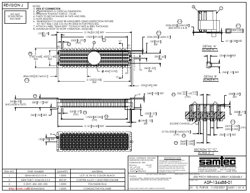
DO NOT SCALE FROM THIS PRINT
NOTES: 1. VITA 57 CONNECTOR. 2. C REPRESENTS A CRITICAL DIMENSION. 3. MINIMUM PUSHOUT FORCE: .75 LBS. 4. PARTS TO BE PACKAGED IN TAPE AND REEL. 5. NOTE DELETED. 6. DIMENSION C10 MUST BE MEASURED USING INSPECTION FIXTURE AT-1817-836-1,USE CO-AU-WI-2003-M FOR PROCESS. 7. ATTACH LABEL "SEAX-0001" TO EACH TAPE & REEL PACKAGE. 8. MAXIMUM ROW TO ROW VARIATION .003[0.08]. 2.196 55.78 REF .123 3.12 REF 1.9500 49.530 .0500 1.270 (TYP) C7 3
SHEET 2 OF 4
REVISION J
NOTES: STENCIL TO BE .0060[.152] THICK.
RECOMMENDED STENCIL LAYOUT FOR ASP-134488-01
1.950 49.53 .0500 1.270
C L 01
A B C D
.450 11.43
.0645 1.638 .0530 1.346
SECTION "C"-"C" SCALE 3 : 1
UNLESS OTHERWISE SPECIFIED, DIMENSIONS ARE IN INCHES. TOLERANCES ARE:
1n4148中文

VF
1
V
IF = 100 mA
1N4448-TR
VF
1
V
Reverse current反向电流
VR = = 20 V, Tj =150℃
IR
50
μA
VR = 75 V
IR
5
μA
Breakdown voltage击穿电压
IR = 100 μA, tp/T = 0.01, tp = 0.3 ms
1N4148中文资料
特征:
•硅外延平面二极管
•电性能相当于二极管:1N4148-1N914 1N4448-1N914B
应用:
快速开关
Absolute Maximum Ratings datasheet绝对最大额定值Tamb =25℃除非另有说明
Tamb =25℃, unless otherwise specified二極體
Tamb =25℃, unless otherwise specified
Parameter参数
Test condition测试条件
Part
Symbol符号
最小
最大
Unit单位
Forward voltage正向电压(压降)
IF = 5 mA
1N4448-TR
VF
0.62
0.72
V
IF = 10 mA
trr
8
ns
IF = 10mA, VR = 6V, iR = 0.1 x IR, RL = 100 Ω
trr
4
ns
特性曲线:
正向电压与结温正向电流与正向电压
正向电流与正向电压反向电流与反向电压
封装及外形:
1N4448W-TP;中文规格书,Datasheet资料
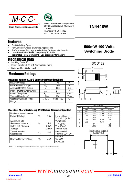
1N4448W500mW 100 Volts Switching Diodeomp onents 20736 Marilla Street Chatsworth! "# $ % ! "#TMMicro Commercial ComponentsFeaturesx Fast Switching Speedx For General Purpose Switching Applicationsx Surface Mount Package Ideally Suited for Automatic Insertion Mechanical Data• Lead Free Finish/RoHS Compliant ("P" Suffixdesignates RoHS Compliant. See ordering information)Admissable Power Dissipation - MilliWatts versus Ambient Temperature - °CFigure 2Forward Derating Curve17550751001250100200300Single Phase, Half Wave60Hz Resistive or Inductive Load MilliWatts°C150400500600Junction Capacitance - pF v ersus Reverse Voltage - VoltsInstantaneous Forward Current - Amperes versus Instantaneous Forward Voltage - VoltsFigure 1Typical Forward Characteristics 4060200100MilliAmps .4.6.8 1.01.21.4.1.2.4.61246102025°CVoltsFigure 3Junction Capacitance.1.21.421020404100200.1.2.61210pFVolts64.44001000T J =25°C1N4448WTMMicro Commercial Components1N4448W11004010********Figure 5Peak Forward Surge Current Peak Forward Surge Current - Amperes versusNumber Of Cycles At 60Hz - CyclesMilliAmpsCycles261020608040400500600Figure 4Typical Reverse Characteristics Instantaneous Reverse Leakage Current - NanoAmperes versus Junction Temperature - °CT J4060200100NanoAmps20120406080100.1.2.4.612461020T A =25°C 4006001000140T A =100°CTMMicro Commercial ComponentsMicro Commercial ComponentsOrdering InformationDevice Packing (Part Number)-TP Tape&Reel:3Kpcs/Reel***IMPORTANT NOTICE***Micro Commercial Components Corp. reserve s the right to make changes without further notice to any product herein tomake corrections, modifications , enhancements , improvements , or other changes . Micro Commercial ComponentsCorp . does not assume any liability arising out of the application or use of any product described herein; neither does itconvey any license under its patent rights ,nor the rights of others . The user of products in such applications shall assume allrisks of such use and will agree to hold Micro Commercial Components Corp . and all the companies whose products arerepresented on our website, harmless against all damages.***LIFE SUPPORT***MCC's products are not authorized for use as critical components in life support devices or systems without the express writtenapproval of Micro Commercial Components Corporation.***CUSTOMER AWARENESS***Counterfeiting of semiconductor parts is a growing problem in the industry. Micro Commercial Components (MCC) is takingstrong measures to protect ourselves and our customers from the proliferation of counterfeit parts. MCC strongly encouragescustomers to purchase MCC parts either directly from MCC or from Authorized MCC Distributors who are listed by country onour web page cited below. Products customers buy either from MCC directly or from Authorized MCC Distributors are genuineparts, have full traceability, meet MCC's quality standards for handling and storage. MCC will not provide any warrantycoverage or other assistance for parts bought from Unauthorized Sources. MCC is committed to combat this globalproblem and encourage our customers to do their part in stopping this practice by buying direct or from authorizeddistributors.分销商库存信息: MICRO-COMMERICAL-CO 1N4448W-TP。
LTC4446EMS8E#PBF;LTC4446EMS8E#TRPBF;LTC4446IMS8E#PBF;LTC4446IMS8E#TRPBF;中文规格书,Datasheet资料
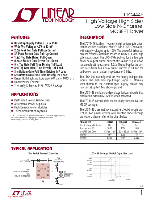
14446fTYPICAL APPLICATIONFEATURESAPPLICATIONSDESCRIPTIONLow Side N-ChannelMOSFET DriverThe L TC ®4446 is a high frequency high voltage gate driver that drives two N-channel MOSFETs in a DC/DC converter with supply voltages up to 100V . The powerful driver ca-pability reduces switching losses in MOSFETs with high gate capacitance. The L TC4446’s pull-up for the top gate driver has a peak output current of 2.5A and its pull-down has an output impedance of 1.2Ω. The pull-up for the bot-tom gate driver has a peak output current of 3A and the pull-down has an output impedance of 0.55Ω.The L TC4446 is confi gured for two supply-independent inputs. The high side input logic signal is internally level-shifted to the bootstrapped supply, which may function at up to 114V above ground.The L TC4446 contains undervoltage lockout circuits that disable the external MOSFETs when activated. The L TC4446 is available in the thermally enhanced 8-lead MSOP package.The L TC4446 does not have adaptive shoot-through pro-tection. For similar drivers with adaptive shoot-through protection, please refer to the chart below.PARAMETER L TC4446L TC4444L TC4444-5Shoot-Through Protection No Yes Yes Absolute Max TS 100V 100V 100V MOSFET Gate Drive 7.2V to 13.5V 7.2V to 13.5V 4.5V to 13.5VV CC UV +6.6V 6.6V 4V V CC UV– 6.15V 6.15V 3.55V nBootstrap Supply Voltage Up to 114V n Wide V CCVoltage: 7.2V to 13.5V n 2.5A Peak Top Gate Pull-Up Current n 3A Peak Bottom Gate Pull-Up Current n 1.2Ω Top Gate Driver Pull-Down n 0.55Ω Bottom Gate Driver Pull-Down n 5ns Top Gate Fall Time Driving 1nF Load n 8ns Top Gate Rise Time Driving 1nF Load n 3ns Bottom Gate Fall Time Driving 1nF Load n 6ns Bottom Gate Rise Time Driving 1nF Loadn Drives Both High and Low Side N-Channel MOSFETs n Undervoltage Lockoutn Thermally Enhanced 8-Pin MSOP PackagenDistributed Power Architecturesn Automotive Power Supplies n High Density Power Modules n Telecommunication SystemsT wo Switch Forward ConverterL TC4446 Driving a 1000pF Capacitive LoadL , L T , L TC and L TM are registered trademarks of Linear Technology Corporation. All other trademarks are the property of their respective owners. Protected by U.S. Patents including 6677210.V BINP 5V/DIVBG 10V/DIV TINP 5V/DIV TG-TS 10V/DIV20ns/DIV4446 TA01b/24446fPIN CONFIGURATIONABSOLUTE MAXIMUM RATINGSSupply VoltageV CC.........................................................–0.3V to 14V BOOST – TS ...........................................–0.3V to 14V TINP Voltage .................................................–2V to 14V BINP Voltage .................................................–2V to 14V BOOST Voltage ........................................–0.3V to 114V TS Voltage ...................................................–5V to 100V Operating Temperature Range (Note 2)....–40°C to 85°C Junction Temperature (Note 3) .............................125°C Storage Temperature Range ...................–65°C to 150°C Lead Temperature (Soldering, 10 sec) ..................300°C(Note 1)1234TINP BINP V CC BG8765TS TG BOOST NCTOP VIEW9MS8E PACKAGE 8-LEAD PLASTIC MSOPT JMAX = 125°C, θJA = 40°C/W , θJC = 10°C/W (NOTE 4)EXPOSED PAD (PIN 9) IS GND, MUST BE SOLDERED TO PCBORDER INFORMATIONELECTRICAL CHARACTERISTICSSYMBOL PARAMETER CONDITIONSMIN TYP MAX UNITS Gate Driver Supply, V CC V CC Operating Voltage7.213.5V I VCCDC Supply Current TINP = BINP = 0V350550μA UVLO Undervoltage Lockout ThresholdV CC Rising V CC Falling Hysteresis l l6.005.606.606.154507.206.70V V mV Bootstrapped Supply (BOOST – TS)I BOOSTDC Supply Current TINP = BINP = 0V 0.12μA Input Signal (TINP , BINP)V IH(BG)BG Turn-On Input Threshold BINP Ramping High l 2.25 2.75 3.25V V IL(BG)BG Turn-Off Input Threshold BINP Ramping Low l 1.85 2.3 2.75V V IH(TG)TG Turn-On Input Threshold TINP Ramping High l 2.25 2.75 3.25V V IL(TG)TG Turn-Off Input Threshold TINP Ramping Lowl 1.852.3 2.75V I TINP(BINP)Input Pin Bias Current ±0.01±2μA High Side Gate Driver Output (TG)V OH(TG)TG High Output Voltage I TG = –10mA, V OH(TG) = V BOOST – V TG 0.7V V OL(TG)TG Low Output Voltage I TG = 100mA, V OL(TG) = V TG –V TSl 120220mV I PU(TG)TG Peak Pull-Up Current l 1.72.5A R DS(TG)TG Pull-Down Resistance l1.22.2ΩThe l denotes the specifi cations which apply over the full operating temperature range, otherwise specifi cations are at T A = 25°C. V CC = V BOOST = 12V , V TS = GND = 0V , unless otherwise noted.LEAD FREE FINISH TAPE AND REEL PART MARKING*PACKAGE DESCRIPTION TEMPERATURE RANGE L TC4446EMS8E#PBF L TC4446EMS8E#TRPBF L TDPZ 8-Lead Plastic MSOP –40°C to 85°C L TC4446IMS8E#PBFL TC4446IMS8E#TRPBFL TDPZ8-Lead Plastic MSOP–40°C to 85°CConsult L TC Marketing for parts specifi ed with wider operating temperature ranges. *The temperature grade is identifi ed by a label on the shipping container .Consult L TC Marketing for information on non-standard lead based fi nish parts.For more information on lead free part marking, go to: http://www.linear .com/leadfree/ For more information on tape and reel specifi cations, go to: http://www.linear .com/tapeandreel//34446fNote 1: Stresses beyond those listed under Absolute Maximum Ratings may cause permanent damage to the device. Exposure to any Absolute Maximum Rating condition for extended periods may affect device reliability and lifetime.Note 2: The L TC4446E is guaranteed to meet specifi cations from 0°C to 85°C. Specifi cations over the –40°C to 85°C operatingtemperature range are assured by design, characterization and correlationELECTRICAL CHARACTERISTICS The l denotes the specifi cations which apply over the full operatingtemperature range, otherwise specifi cations are at T A = 25°C. V CC = V BOOST = 12V , V TS = GND = 0V , unless otherwise noted.SYMBOL PARAMETERCONDITIONSMINTYP MAXUNITS Low Side Gate Driver Output (BG)V OH(BG)BG High Output Voltage I BG = –10mA, V OH(BG) = V CC – V BG0.7VV OL(BG)BG Low Output Voltage I BG = 100mAl 55110mV I PU(BG)BG Peak Pull-Up Current l 23A R DS(BG)BG Pull-Down Resistance l0.55 1.1ΩSwitching Time (BINP (TINP) is Tied to Ground While TINP (BINP) is Switching. Refer to Timing Diagram)t PLH(TG)TG Low-High (Turn-On) Propagation Delay l 2545ns t PHL(TG)TG High-Low (Turn-Off) Propagation Delay l 2240ns t PLH(BG)BG Low-High (Turn-On) Propagation Delay l 1935ns t PHL(BG)BG High-Low (Turn-Off) Propagation Delay l 1430ns t DM(BGTG)Delay Matching BG Turn-Off and TG Turn-On l –151035ns t DM(TGBG)Delay Matching TG Turn-Off and BG Turn-On l –25–325ns t r(TG)TG Output Rise Time 10% – 90%, C L = 1nF 10% – 90%, C L = 10nF880ns ns t f(TG)TG Output Fall Time 10% – 90%, C L = 1nF 10% – 90%, C L = 10nF550ns ns t r(BG)BG Output Rise Time 10% – 90%, C L = 1nF 10% – 90%, C L = 10nF660ns ns t f(BG)BG Output Fall Time 10% – 90%, C L = 1nF 10% – 90%, C L = 10nF 330ns nswith statistical process controls. The L TC4446I is guaranteed over the full –40°C to 85°C operating temperature range.Note 3: T J is calculated from the ambient temperature T A and power dissipation P D according to the following formula: T J = T A + (P D • θJA °C/W)Note 4: Failure to solder the exposed back side of the MS8E package to the PC board will result in a thermal resistance much higher than 40°C/W .TYPICAL PERFORMANCE CHARACTERISTICSV CC Supply Quiescent Current vs VoltageBOOST-TS Supply Quiescent Current vs VoltageV CC Supply Current vs TemperatureV CC SUPPL Y VOL TAGE (V)00Q U I E S C E N T C U R R E N T (μA )501502002506789101112134504446 G011001234514300350400BOOST SUPPL Y VOL TAGE (V)00Q U I E S C E N T C U R R E N T (μA )501502002506789101112134004446 G021001234514300350TEMPERATURE (°C)V C C S U P P L Y C U R R E N T (μA )3503603704446 G03330300–40–25–105203550658095110125380340320310/44446fTYPICAL PERFORMANCE CHARACTERISTICSBoost Supply Current vs TemperatureOutput Low Voltage (V OL ) vs Supply VoltageOutput High Voltage (V OH ) vs Supply VoltageInput Thresholds (TINP , BINP) vs Supply VoltageInput Thresholds (TINP , BINP) vs TemperatureInput Thresholds (TINP , BINP) Hysteresis vs VoltageInput Thresholds (TINP , BINP) Hysteresis vs TemperatureV CC Undervoltage Lockout Thresholds vs TemperatureRise and Fall Time vs V CC Supply VoltageTEMPERATURE (°C)B O O S T S U P P L YC U R R E N T (μA )2503003504446 G041500–40–25–10520355065809511012540020010050SUPPL Y VOL TAGE (V)7O U T P U T V O L T A G E (m V )140104446 G058040891120016012010060121314SUPPL Y VOL TAGE (V)75T G O R B G O U T P U T V O L T A G E (V )689101512911124446 G0671314118101314SUPPL Y VOL TAGE (V)72.1T G O R B G I N P U T T H R E S H O L D (V )2.22.42.52.63.12.8911124446 G072.32.93.02.78101314TEMPERATURE (°C)–25T G O R B G I N P U T T H R E S H O L D (V )2.62.83.0954446 G082.42.22.52.72.92.32.12.053565–10–40110205080125SUPPL Y VOL TAGE (V)78375T G O R B G I N P U T T H R E S H OL D H Y S T E R E S I S (m V )425500911124446 G09400475450101314TEMPERATURE (°C)–40–25375T G O R B G I N P U T T H R E S H O L D H Y S T E R E S I S(m V )425500–105205065804446 G104004754503511095125TEMPERATURE (°C)–406.0V C C S U P L L Y V O L T A G E (V )6.16.36.46.56.7–2535654446 G116.26.62095125110–1055080SUPPL Y VOL TAGE (V)7R I S E /F A L L T I M E (n s )122830222632911124446 G12820161024618148101314/54446fTYPICAL PERFORMANCE CHARACTERISTICSRise and Fall Time vs Load CapacitancePeak Driver (TG, BG) Pull-Up Current vs TemperatureOutput Driver Pull-Down Resistance vs TemperaturePropagation Delay vs V CC Supply VoltagePropagation Delay vs TemperatureLOAD CAPACITANCE (nF)1R I S E /F A L L T I M E (n s )40506094445 G1330200357210468108070TEMPERATURE (°C)–402.0P U L L -U P C U R R E N T (A )2.22.62.83.03.4–2535654446 G142.43.22095125110–1055080TEMPERATURE (°C)–25O U T P U T D R I V E R P U L L -D O W N R E S I S T A C N E (Ω)1.21.62.0954446 G150.80.41.01.41.80.60.253565–10–40110205080125SUPPL Y VOL TAGE (V)710P R O P A G A T I O N D E L A Y (n s )121618203024911124444 G16142628228101314TEMPERATURE (°C)–402P R O P A G A T I O N D E L A Y (n s )717222737–2535654446 G1712322095125110–1055080Switching Supply Current vs Input FrequencySwitching Supply Current vs Load CapacitanceSWITCHING FREQUENCY (kHz)S U P P L Y C U R R E N T (m A )1.52.02.560010004446 G181.00.502004008003.03.54.0LOAD CAPACITANCE (nF)1S U P P L Y C U R R E N T (m A )1010013450.127896104446 G19/64446fPIN FUNCTIONSBLOCK DIAGRAMTINP (Pin 1): High Side Input Signal. Input referenced to GND. This input controls the high side driver output (TG).BINP (Pin 2): Low Side Input Signal. This input controls the low side driver output (BG).V CC (Pin 3): Supply. This pin powers input buffers, logic and the low side gate driver output directly and the high side gate driver output through an external diode con-nected between this pin and BOOST (Pin 6). A low ESR ceramic bypass capacitor should be tied between this pin and GND (Pin 9).BG (Pin 4): Low Side Gate Driver Output (Bottom Gate). This pin swings between V CC and GND.NC (Pin 5): No Connect. No connection required.BOOST (Pin 6): High Side Bootstrapped Supply. An ex-ternal capacitor should be tied between this pin and TS (Pin 8). Normally, a bootstrap diode is connected between V CC (Pin 3) and this pin. Voltage swing at this pin is from V CC – V D to V IN + V CC – V D , where V D is the forward volt-age drop of the bootstrap diode.TG (Pin 7): High Side Gate Driver Output (Top Gate). This pin swings between TS and BOOST .TS (Pin 8): High Side MOSFET Source Connection (Top Source).Exposed Pad (Pin 9): Ground. Must be soldered to PCB ground for optimal thermal performance.TIMING DIAGRAMTINP (BINP)BG (TG)BINP (TINP)TG (BG)/OPERATIONOverviewThe L TC4446 receives ground-referenced, low voltage digi-tal input signals to drive two N-channel power MOSFETs in a synchronous buck power supply confi guration. The gate of the low side MOSFET is driven either to V CC or GND, depending on the state of the input. Similarly, the gate of the high side MOSFET is driven to either BOOST or TS by a supply bootstrapped off of the switching node (TS). Input StageThe L TC4446 employs CMOS compatible input thresholds that allow a low voltage digital signal to drive standard power MOSF ETs. The LTC4446 contains an internal voltage regulator that biases both input buffers for high side and low side inputs, allowing the input thresholds (V IH = 2.75V, V IL = 2.3V) to be independent of variations inV CC. The 450mV hysteresis between V IH and V IL eliminates false triggering due to noise during switching transitions. However, care should be taken to keep both input pins (TINP and BINP) from any noise pickup, especially in high frequency, high voltage applications. The L TC4446 input buffers have high input impedance and draw negligible input current, simplifying the drive circuitry required for the inputs.Output StageA simplifi ed version of the L TC4446’s output stage is shown in Figure 1. The pull-up devices on the BG and TG outputs are NPN bipolar junction transistors (Q1 and Q2). The BG and TG outputs are pulled up to within an NPN V BE (~0.7V) of their positive rails (V CC and BOOST, respectively). Both BG and TG have N-channel MOSFET pull-down devices (M1 and M2) which pull BG and TG down to their nega-tive rails, GND and TS. The large voltage swing of the BG and TG output pins is important in driving external power MOSFETs, whose R DS(ON) is inversely proportional to the gate overdrive voltage (V GS − V TH).Rise/Fall TimeThe L TC4446’s rise and fall times are determined by the peak current capabilities of Q1 and M1. The predriver that drives Q1 and M1 uses a nonoverlapping transition scheme to minimize cross-conduction currents. M1 is fully turned off before Q1 is turned on and vice versa.Since the power MOSFET generally accounts for the ma-jority of the power loss in a converter, it is important to quickly turn it on or off, thereby minimizing the transition time in its linear region. An additional benefi t of a strong pull-down on the driver outputs is the prevention of cross- conduction current. For example, when BG turns the low side (synchronous) power MOSFET off and TG turns the high side power MOSFET on, the voltage on the TS pin will rise to V IN very rapidly. This high frequency positive voltage transient will couple through the C GD capacitance of the low side power MOSFET to the BG pin. If there is an insuffi cient pull-down on the BG pin, the voltage on the BG pin can rise above the threshold voltage of the low side power MOSFET, momentarily turning it back on. With Figure 1. Capacitance Seen by BG and TG During Switching/74446fOPERATIONboth the high side and low side MOSFETs conducting, signifi cant cross-conduction current will fl ow through the MOSFETs from V IN to ground and will cause substantial power loss. A similar effect occurs on TG due to the C GS and C GD capacitances of the high side MOSFET.The powerful output driver of the L TC4446 reduces the switching losses of the power MOSFET, which increase with transition time. The L TC4446’s high side driver is capable of driving a 1nF load with 8ns rise and 5ns fall times using a bootstrapped supply voltage V BOOST-TS of 12V while its low side driver is capable of driving a 1nF Power DissipationTo ensure proper operation and long-term reliability, the L TC4446 must not operate beyond its maximum tem-perature rating. Package junction temperature can be calculated by:T J = T A + P D (θJA)where:T J = Junction temperatureT A = Ambient temperatureP D = Power dissipationθJA = Junction-to-ambient thermal resistance Power dissipation consists of standby and switching power losses:P D = P DC + P AC + P QGwhere:P DC = Quiescent power lossP AC = Internal switching loss at input frequency, f INP QG = Loss due turning on and off the external MOSFET with gate charge QG at frequency f IN load with 6ns rise and 3ns fall times using a supply volt-age V CC of 12V.Undervoltage Lockout (UVLO)The L TC4446 contains an undervoltage lockout detector that monitors V CC supply. When V CC falls below 6.15V, the output pins BG and TG are pulled down to GND and TS, respectively. This turns off both external MOSFETs. When V CC has adequate supply voltage, normal operation will resume.APPLICATIONS INFORMATIONThe L TC4446 consumes very little quiescent current. TheDC power loss at V CC = 12V and V BOOST-TS = 12V is only(350μA)(12V) = 4.2mW.At a particular switching frequency, the internal power lossincreases due to both AC currents required to charge anddischarge internal node capacitances and cross-conduc-tion currents in the internal logic gates. The sum of thequiescent current and internal switching current with noload are shown in the Typical Performance Characteristicsplot of Switching Supply Current vs Input Frequency.The gate charge losses are primarily due to the large ACcurrents required to charge and discharge the capacitanceof the external MOSFETs during switching. For identicalpure capacitive loads C LOAD on TG and BG at switchingfrequency f IN, the load losses would be:P CLOAD = (C LOAD)(f)[(V BOOST-TS)2 + (V CC)2]In a typical synchronous buck confi guration, V BOOST-TSis equal to V CC – V D, where V D is the forward voltagedrop across the diode between V CC and BOOST. If thisdrop is small relative to V CC, the load losses can beapproximated as:P CLOAD = 2(C LOAD)(f IN)(V CC)2/84446fAPPLICATIONS INFORMATIONUnlike a pure capacitive load, a power MOSF ET’s gate capacitance seen by the driver output varies with its V GS voltage level during switching. A MOSFET’s capacitive load power dissipation can be calculated using its gate charge, Q G. The Q G value corresponding to the MOSFET’s V GS value (V CC in this case) can be readily obtained from the manufacturer’s Q G vs V GS curves. For identical MOSFETs on TG and BG:P QG = 2(V CC)(Q G)(f IN)To avoid damage due to power dissipation, the L TC4446 includes a temperature monitor that will pull BG and TG low if the junction temperature rises above 160°C. Normal operation will resume when the junction temperature cools to less than 135°C.Bypassing and GroundingThe LTC4446 requires proper bypassing on the V CC and V BOOST-TS supplies due to its high speed switching (nanoseconds) and large AC currents (Amperes). Careless component placement and PCB trace routing may cause excessive ringing.To obtain the optimum performance from the L TC4446: A. Mount the bypass capacitors as close as possible between the V CC and GND pins and the BOOST and TS pins. The leads should be shortened as much as possible to reduce lead inductance.B. Use a low inductance, low impedance ground plane to reduce any ground drop and stray capacitance. Remember that the L TC4446 switches greater than 3A peak currents and any signifi cant ground drop will degrade signal integrity.C. Plan the power/ground routing carefully. Know where the large load switching current is coming from and going to. Maintain separate ground return paths for the input pin and the output power stage.D. Keep the copper trace between the driver output pin and the load short and wide.E. Be sure to solder the Exposed Pad on the back side of the L TC4446 package to the board. Correctly soldered to a 2500mm2 doublesided 1oz copper board, the L TC4446 has a thermal resistance of approximately 40°C/W for the MS8E package. Failure to make good thermal contact between the exposed back side and the copper board will result in thermal resistances far greater than 40°C/W./94446f104446fTYPICAL APPLICATIONL T C 3722/L T C 4446 420W 36V -72V I N t o 12V /35A I s o l a t e d F u l l -B r i d g e S u p p l yL 1V I –V I 36V T /分销商库存信息:LINEAR-TECHNOLOGYLTC4446EMS8E#PBF LTC4446EMS8E#TRPBF LTC4446IMS8E#PBF LTC4446IMS8E#TRPBF。
744770133;中文规格书,Datasheet资料
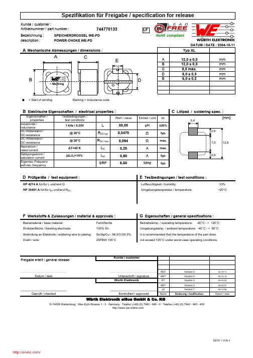
Bezeichnung :description := Start of winding Marking = Inductance code33% Umgebungstemperatur / temperature:+20°C100% SnMST 04-10-11MST 03-12-10RT 03-03-03MST02-03-27JH 00-12-06NameDatum / dateIt is recommended that the temperature of the part does not exceed 125°C under worst case operating conditions.Anbindung an Elektrode / soldering wire to plating:Sn/Ag/Cu - 96.5/3.0/0.5%Draht / wire:2SFBW 155°CUmgebungstemp. / ambient temperature: -40°C - + 85°C Freigabe erteilt / general release:Kunde / customerWürth Elektronik....................................................................................................................................................................Unterschrift / signature Ferrit/ferrite F Werkstoffe & Zulassungen / material & approvals :G Eigenschaften / general specifications :D Prüfgeräte / test equipment :E Testbedingungen / test conditions :Basismaterial / base material:Betriebstemp. / operating temperature: -40°C - + 125°C D-74638 Waldenburg · Max-Eyth-Strasse 1 - 3 · Germany · Telefon (+49) (0) 7942 - 945 - 0 · Telefax (+49) (0) 7942 - 945 - 400Geprüft / checked ..........................................................................................................................Kontrolliert / approvedWürth Elektronik eiSos GmbH & Co. KG744770133SPEICHERDROSSEL WE-PDPOWER-CHOKE WE-PDArtikelnummer / part number : Luftfeuchtigkeit / humidity:HP 4274 A für/for L und/and Q HP 34401 A für/for I DC und/and R DCÄnderung / modificationVersion 1Version 2Version 3Version 4Version 5 Datum / dateEndoberfläche / finishing electrode:• MarkingRoHS compliantLFdescription :MST 04-10-11MST 03-12-10RT 03-03-03MST02-03-27JH 00-12-06NameDatum / dateH Induktivitätskurve / Inductance curve :POWER-CHOKE WE-PDDATUM / DATE : 2004-10-11Kontrolliert / approvedDatum / dateUnterschrift / signature Würth ElektronikWürth Elektronik eiSos GmbH & Co. KGD-74638 Waldenburg · Max-Eyth-Strasse 1 - 3 · Germany · Telefon (+49) (0) 7942 - 945 - 0 · Telefax (+49) (0) 7942 - 945 - 400Freigabe erteilt / general release:Kunde / customer..................................................................................................................................................................................................................................................................................Geprüft / checked Version 4Version 5Änderung / modificationVersion 1Version 2Version 3a 330,0± 0,5mmb 20,20± 0,2mm+ 0,5- 1,0d 100,0± 0,2mmMST 04-10-11MST 03-12-10RT 03-03-03MST02-03-27JH 00-12-06NameDatum / dateRollenspezifikation / Reel specification:Freigabe erteilt / general release:Kunde / customerc 13,00mm....................................................................................................................................................................Datum / dateUnterschrift / signature Würth Elektronik..........................................................................................................................Würth Elektronik eiSos GmbH & Co. KGGeprüft / checked Kontrolliert / approvedD-74638 Waldenburg · Max-Eyth-Strasse 1 - 3 · Germany · Telefon (+49) (0) 7942 - 945 - 0 · Telefax (+49) (0) 7942 - 945 - 400Änderung / modificationVersion 1Version 2Version 3Version 4Version 5The force for tearing off cover tape is 10 to 130 grams in arrow direction165 to 180°feeding directionThis electronic component is designed and developed with the intention for use in general electronics equipments. Before incorporating the components into any equipments in the field such as aerospace, aviation, nuclear control, submarine, transportation, (automotive control, train control, ship control), transportation signal, disaster prevention, medical, public information network etc. where higher safety and reliability are especially required or if there is possibility of direct damage or injury to human body. In addition, even electronic component in general electronic equipments, when used in electrical circuits that require high safety, reliability functions or performance, the sufficient reliability evaluation-check for the safety must be performed before use. It is essential to give consideration when to install a protective circuit at the design stage.分销商库存信息: WURTH-ELECTRONICS 744770133。
LTC4449EDCB#TRMPBF;LTC4449EDCB#TRPBF;LTC4449IDCB#TRMPBF;LTC4449IDCB#TRPBF;中文规格书,Datasheet资料
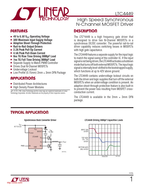
SYMBOL
PARAMETER
CONDITIONS
MIN TYP MAX UNITS
Input Signal (IN)
VIH(TG)
TG Turn-On Input Threshold
VIL(TG)
TG Turn-Off Input Threshold
VIH(BG)
BG Turn-On Input Threshold
FEATURES
n 4V to 6.5V VCC Operating Voltage n 38V Maximum Input Supply Voltage n Adaptive Shoot-Through Protection n Rail-to-Rail Output Drivers n 3.2A Peak Pull-Up Current n 4.5A Peak Pull-Down Current n 8ns TG Rise Time Driving 3000pF Load n 7ns TG Fall Time Driving 3000pF Load n Separate Supply to Match PWM Controller n Drives Dual N-Channel MOSFETs n Undervoltage Lockout n Low Profile (0.75mm) 2mm × 3mm DFN Package
IN = Floating
VCC Rising VCC Falling Hysteresis
4
6.5
V
300
400
μA
l 2.75 3.20 3.65
V
l 2.60 3.04 3.50
V
160
mV
LS4148-GS08中文资料
LS4148/LS4448Document Number 85561Rev. 1.8, 04-May-07Vishay Semiconductors19612009Small Signal Fast Switching DiodesFeatures•Silicon Epitaxial Planar Diodes•Electrical data identical with the devices1N4148 and 1N4448 respectively•Quadro Melf package•Lead (Pb)-free component•Component in accordance to RoHS 2002/95/EC and WEEE 2002/96/ECApplications•Extremely fast switchesMechanical DataCase: QuadroMELF Glass case (SOD80)Weight: approx. 34 mgCathode Band Color: Black Packaging Codes/Options:GS18/10 k per 13" reel (8 mm tape), 10 k/box GS08/2.5 k per 7" reel (8 mm tape), 12.5 k/boxParts TableAbsolute Maximum RatingsT amb = 25°C, unless otherwise specifiedThermal CharacteristicsT amb = 25°C, unless otherwise specifiedPartType differentiationOrdering codeType MarkingRemarks LS4148V F = max. 1000 mV at I F = 50 mA LS4148-GS18 or LS4148-GS08-T ape and Reel LS4448V F = max. 1000 mV at I F = 100 mALS4448-GS18 or LS4448-GS08-T ape and ReelParameterT est conditionSymbol Value Unit Repetitive peak reverse voltage V RRM 100V Reverse voltageV R 75V Peak forward surge current t p = 1 µsI FSM 2A Repetitive peak forward current I FRM 500mA Forward continuous current I F 300mA Average forward current V R = 0I FAV 150mA Power dissipationP tot500mWParameterT est conditionSymbol Value Unit Thermal resistance junction to ambient air on PC board 50 mm x 50 mm x 1.6mm R thJA 500K/W Junction temperature T j 175°C Storage temperature rangeT stg- 65 to + 175°C 2Document Number 85561Rev. 1.8, 04-May-07LS4148/LS4448Vishay Semiconductors Electrical CharacteristicsT amb = 25°C, unless otherwise specifiedTypical CharacteristicsT amb = 25°C, unless otherwise specifiedParameterTest conditionPart Symbol Min Typ.Max Unit Forward voltageI F = 5 mA LS4448V F 620720mV I F = 50 mA LS4148V F 8601000mV I F = 100 mALS4448V F 9301000mV Reverse currentV R = 20 VI R 25nA VR = 20 V , T j = 150°C I R 50µA V R= 75 VI R 5µA Breakdown voltage I R = 100 µA, t p /T = 0.01, t p = 0.3 msV (BR)100V Diode capacitance V R = 0, f = 1 MHz, V HF = 50 mV C D 4pF Rectification efficiency V HF = 2 V , f = 100 MHz ηr 45%Reverse recovery timeI F = I R = 10 mA, i R = 1 mA t rr 8ns I F = 10 mA, V R = 6 V , i R = 0.1 x I R , R L = 100 Ωt rr4nsFigure 1. Forward Current vs. Forward Voltage Figure 2. Forward Current vs. Forward Voltage 00.40.81.21.60.11101001000I F - F o r w a r d C u r r e n t (m A )V F - For w ard V oltage (V ) 2.0166400.40.81.21.60.11101001000I F - F o r w a r d C u r r e n t (m A )V F - For w ard V oltage (V ) 2.016642Figure 3. Reverse Current vs. Reverse VoltageFigure 4. Diode Capacitance vs. Reverse VoltageI R - R e v e r s e C u r r e n t (n A )V R - Re v erse V oltage (V )101 100 94 90980.111000.51.01.52.03.0C D - D i o d e C a p a c i t a n c e (p F )10094 90992.5V R - Re v erse V oltage (V )LS4148/LS4448Document Number 85561Rev. 1.8, 04-May-07Vishay Semiconductors3Package Dimensions in millimeters (inches):Quadro MELF SOD80 4Document Number 85561Rev. 1.8, 04-May-07LS4148/LS4448Vishay SemiconductorsOzone Depleting Substances Policy StatementIt is the policy of Vishay Semiconductor GmbH to1.Meet all present and future national and international statutory requirements.2.Regularly and continuously improve the performance of our products, processes, distribution and operatingsystems with respect to their impact on the health and safety of our employees and the public, as well as their impact on the environment.It is particular concern to control or eliminate releases of those substances into the atmosphere which are known as ozone depleting substances (ODSs).The Montreal Protocol (1987) and its London Amendments (1990) intend to severely restrict the use of ODSs and forbid their use within the next ten years. Various national and international initiatives are pressing for an earlier ban on these substances.Vishay Semiconductor GmbH has been able to use its policy of continuous improvements to eliminate the use of ODSs listed in the following documents.1.Annex A, B and list of transitional substances of the Montreal Protocol and the London Amendmentsrespectively2.Class I and II ozone depleting substances in the Clean Air Act Amendments of 1990 by the EnvironmentalProtection Agency (EPA) in the USA3.Council Decision 88/540/EEC and 91/690/EEC Annex A, B and C (transitional substances) respectively. Vishay Semiconductor GmbH can certify that our semiconductors are not manufactured with ozone depleting substances and do not contain such substances.We reserve the right to make changes to improve technical designand may do so without further notice.Parameters can vary in different applications. All operating parameters must be validated for each customer application by the customer. Should the buyer use Vishay Semiconductors products for any unintended or unauthorized application, the buyer shall indemnify Vishay Semiconductors against all claims, costs, damages, and expenses, arising out of, directly or indirectly, any claim of personal damage, injury or death associatedwith such unintended or unauthorized use.Vishay Semiconductor GmbH, P.O.B. 3535, D-74025 Heilbronn, GermanyDocument Number: 91000Revision: 18-Jul-081DisclaimerLegal Disclaimer NoticeVishayAll product specifications and data are subject to change without notice.Vishay Intertechnology, Inc., its affiliates, agents, and employees, and all persons acting on its or their behalf (collectively, “Vishay”), disclaim any and all liability for any errors, inaccuracies or incompleteness contained herein or in any other disclosure relating to any product.Vishay disclaims any and all liability arising out of the use or application of any product described herein or of any information provided herein to the maximum extent permitted by law. The product specifications do not expand or otherwise modify Vishay’s terms and conditions of purchase, including but not limited to the warranty expressed therein, which apply to these products.No license, express or implied, by estoppel or otherwise, to any intellectual property rights is granted by this document or by any conduct of Vishay.The products shown herein are not designed for use in medical, life-saving, or life-sustaining applications unless otherwise expressly indicated. Customers using or selling Vishay products not expressly indicated for use in such applications do so entirely at their own risk and agree to fully indemnify Vishay for any damages arising or resulting from such use or sale. Please contact authorized Vishay personnel to obtain written terms and conditions regarding products designed for such applications.Product names and markings noted herein may be trademarks of their respective owners.元器件交易网。
VISHAY SEMICONDUCTOR - LL4148 LL4448 数据手册
LL4148 / LL4448Document Number 85557Rev. 1.8, 24-Mar-06Vishay Semiconductors1949371Small Signal Fast Switching DiodesFeatures•Silicon Epitaxial Planar Diodes•Electrical data identical with the devices1N4148 and 1N4448 respectively•Lead (Pb)-free component •Component in acc. to RoHS 2002/95/EC and WEEE 2002/96/ECApplications•Extreme fast switchesMechanical DataCase: MiniMELF Glass case (SOD80)Weight: approx. 31 mgCathode Band Color: Black Packaging Codes/Options:GS18 / 10 k per 13" reel (8 mm tape), 10 k/box GS08 / 2.5 k per 7" reel (8 mm tape), 12.5 k/boxParts TableAbsolute Maximum RatingsT amb = 25°C, unless otherwise specifiedThermal CharacteristicsT amb = 25°C, unless otherwise specifiedPartType differentiationOrdering codeRemarks LL4148V RRM = 100 V , V F = max. 1000 mV at I F = 50 mA LL4148-GS18 or LL4148-GS08Tape and Reel LL4448V RRM = 100 V , V F = max. 1000 mV at I F = 100 mALL4448-GS18 or LL4448-GS08Tape and ReelParameterT est conditionSymbol Value Unit Repetitive peak reverse voltage V RRM 100V Reverse voltageV R 75V Peak forward surge current t p = 1 µsI FSM 2A Repetitive peak forward current I FRM 500mA Forward continuous current I F 300mA Average forward current V R = 0I FAV 150mA Power dissipationP V500mWParameterT est conditionSymbol Value Unit Junction to ambient air on PC board50 mm x 50 mm x 1.6 mmR thJA 500K/W Junction temperature T j 175°C Storage temperature rangeT stg- 65 to + 175°C 2Document Number 85557Rev. 1.8, 24-Mar-06LL4148 / LL4448Vishay Semiconductors Electrical CharacteristicsT amb = 25°C, unless otherwise specifiedTypical CharacteristicsT amb = 25°C, unless otherwise specifiedParameterTest conditionPart Symbol Min Typ.Max Unit Forward voltageI F = 5 mA LL4448V F 620720mV I F = 50 mA LL4148V F 8601000mV I F = 100 mALL4448V F 9301000mV Reverse currentV R = 20 VI R 25nA V R = 20 V , T j = 150°C I R 50µA V R = 75 VI R 5µA Breakdown voltage I R = 100 µA, tp /T = 0.01, t p = 0.3 msV (BR)100V Diode capacitance V R = 0, f = 1 MHz, V HF = 50 mV C D 4pF Rectification efficiency V HF = 2 V , f = 100 MHz ηr 45%Reverse recovery timeI F = I R = 10 mA, i R = 1 mAt rr 8ns I F = 10 mA, V R = 6 V , i R = 0.1 x I R , R L = 100 Ωt rr4nsFigure 1. Forward Current vs. Forward Voltage 00.40.81.21.60.11101001000I -F o r w a r d C u r r e n t (m A )F V F -For w ard V oltage (V )94 9096Figure 2. Forward Current vs. Forward Voltage9490970.40.81.21.60.11101001000I -F o r w a r d C u r r e n t (m A )F V F -For w ard V oltage (V )2.0LL4148 / LL4448Document Number 85557Rev. 1.8, 24-Mar-06Vishay Semiconductors3Package Dimensions in mm (Inches)Figure 3. Reverse Current vs. Reverse VoltageI - R e v e r s e C u r r e n t (n A )R V R -Re v erse V oltage (V )101 100949098Figure 4. Diode Capacitance vs. Reverse Voltage0.111000.51.01.52.03.0C -D i o d e C a p a c i t a n c e (p F )D 10094 90992.5V R -Re v erse V oltage (V ) 4Document Number 85557Rev. 1.8, 24-Mar-06LL4148 / LL4448Vishay SemiconductorsOzone Depleting Substances Policy StatementIt is the policy of Vishay Semiconductor GmbH to1.Meet all present and future national and international statutory requirements.2.Regularly and continuously improve the performance of our products, processes, distribution and operatingsystems with respect to their impact on the health and safety of our employees and the public, as well as their impact on the environment.It is particular concern to control or eliminate releases of those substances into the atmosphere which are known as ozone depleting substances (ODSs).The Montreal Protocol (1987) and its London Amendments (1990) intend to severely restrict the use of ODSs and forbid their use within the next ten years. Various national and international initiatives are pressing for an earlier ban on these substances.Vishay Semiconductor GmbH has been able to use its policy of continuous improvements to eliminate the use of ODSs listed in the following documents.1.Annex A, B and list of transitional substances of the Montreal Protocol and the London Amendmentsrespectively2.Class I and II ozone depleting substances in the Clean Air Act Amendments of 1990 by the EnvironmentalProtection Agency (EPA) in the USA3.Council Decision 88/540/EEC and 91/690/EEC Annex A, B and C (transitional substances) respectively. Vishay Semiconductor GmbH can certify that our semiconductors are not manufactured with ozone depleting substances and do not contain such substances.We reserve the right to make changes to improve technical designand may do so without further notice.Parameters can vary in different applications. All operating parameters must be validated for each customer application by the customer. Should the buyer use Vishay Semiconductors products for any unintended or unauthorized application, the buyer shall indemnify Vishay Semiconductors against all claims, costs, damages, and expenses, arising out of, directly or indirectly, any claim of personal damage, injury or death associated with such unintended or unauthorized use.Vishay Semiconductor GmbH, P.O.B. 3535, D-74025 Heilbronn, GermanyLegal Disclaimer NoticeVishay Document Number: Revision: 08-Apr-051NoticeSpecifications of the products displayed herein are subject to change without notice. Vishay Intertechnology, Inc., or anyone on its behalf, assumes no responsibility or liability for any errors or inaccuracies.Information contained herein is intended to provide a product description only. No license, express or implied, by estoppel or otherwise, to any intellectual property rights is granted by this document. Except as provided in Vishay's terms and conditions of sale for such products, Vishay assumes no liability whatsoever, and disclaims any express or implied warranty, relating to sale and/or use of Vishay products including liability or warranties relating to fitness for a particular purpose, merchantability, or infringement of any patent, copyright, or other intellectual property right. The products shown herein are not designed for use in medical, life-saving, or life-sustaining applications. Customers using or selling these products for use in such applications do so at their own risk and agree to fully indemnify Vishay for any damages resulting from such improper use or sale.。
STF800 SmartLine 单法兰变送器产品说明书
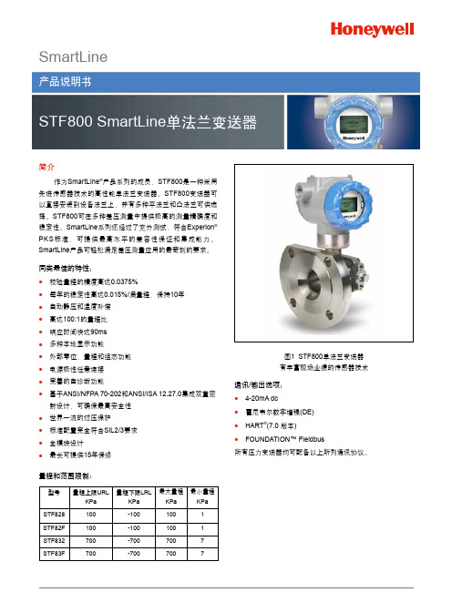
SmartLine简介作为SmartLine ®产品系列的成员,STF800是一种采用先进传感器技术的高性能单法兰变送器。
STF800变送器可以直接安装到设备法兰上,并有多种平法兰和凸法兰可供选择。
STF800可在多种差压测量中提供极高的测量精确度和稳定性。
SmartLine 系列还经过了充分测试,符合Experion ® PKS 标准,可提供最高水平的兼容性保证和集成能力。
SmartLine 产品可轻松满足差压测量应用的最苛刻的要求。
同类最佳的特性:● 校验量程的精度高达0.0375%● 每年的稳定性高达0.015%/满量程,保持10年● 自动静压和温度补偿● 高达100:1的量程比● 响应时间快达90ms ● 多种本地显示功能● 外部零位、量程和组态功能● 电源极性任意连接● 完善的自诊断功能●基于ANSI/NFPA 70-202和ANSI/ISA 12.27.0集成双重密封设计,可确保最高安全性● 世界一流的过压保护● 标准配置完全符合SIL2/3要求● 全模块设计●最长可提供15年保修量程和范围限制:型号量程上限URLKPa量程下限LRLKPa最大量程KPa 最小量程KPa STF828 100-1001001STF82F 100-1001001STF832 700-7007007STF83F700-7007007图1 STF800单法兰变送器有丰富现场业绩的传感器技术通讯/输出选项:●4-20mA dc●霍尼韦尔数字增强(DE)● HART ®(7.0 版本)●FOUNDATION™ Fieldbus所有压力变送器均可配备以上所列通讯协议。
描述SmartLine系列的压力变送器均基于高性能的传感器设计。
这一个传感器实际集成了多个传感器,将过程压力测量与静态压力(DP型号)及温度补偿测量相结合,从而实现了最佳的总体性能。
这一性能使得SmartLine成为几乎可以替代任何现有变送器的竞争产品。
飞利浦 PMLL4148L; PMLL4448 数据手册

1.Product profile1.1General descriptionSingle high-speed switching diodes, fabricated in planar technology, and encapsulated in small hermetically sealed glass SOD80C SMD packages.1.2Featuress Small hermetically sealed glass SMD package s High switching speed:≤ 4 nss Continuous reverse voltage:≤ 75 Vs Repetitive peak reverse voltage:≤ 100 V sRepetitive peak forward current:≤ 450 mA1.3Applicationss High-speed switchings Inverse-polarity protection1.4Quick reference data[1]Device mounted on an FR4 Printed-Circuit Board (PCB), single-sided copper, tin-plated and standard footprint.[2]When switched from I F = 10 mA to I R = 60 mA; R L = 100Ω; measured at I R = 1 mAPMLL4148L; PMLL4448High-speed switching diodesRev. 06 — 4 April 2005Product data sheetTable 1:Product overviewType numberPackage ConfigurationPhilipsJEITA PMLL4148L SOD80C -single diode PMLL4448SOD80C-single diode Table 2:Quick reference data Symbol Parameter ConditionsMin Typ Max Unit I F forward current [1]--200mA I FRM repetitive peak forward current --450mA V R reverse voltage --75V V Fforward voltage I F = 100 mA --1000mV PMLL4148L I F = 10 mA --1000mV PMLL4448I F = 5 mA620-720mV t rrreverse recovery time[2]--4ns查询PMLL4148L供应商2.Pinning information[1]The marking band indicates the cathode.3.Ordering information4.Marking[1]black: made in Philippines brown: made in China5.Limiting valuesTable 3:PinningPin Description Simplified outlineSymbol1cathode [1]2anodekasym006Table 4:Ordering informationType numberPackage NameDescriptionVersion PMLL4148L -hermetically sealed glass surface mounted package;2connectorsSOD80C PMLL4448-hermetically sealed glass surface mounted package;2connectorsSOD80CTable 5:Marking codesType number Marking code [1]PMLL4148L marking band PMLL4448marking bandTable 6:Limiting valuesIn accordance with the Absolute Maximum Rating System (IEC 60134).Symbol ParameterConditions Min Max Unit V RRM repetitive peak reverse voltage -100V V R reverse voltage -75V I F forward current [1]-200mA I FRM repetitive peak forward current-450mAI FSMnon-repetitive peak forward currentsquare wave [2]t p = 1µs -4A t p = 1 ms -1A t p = 1 s-0.5A P tottotal power dissipationT amb = 25°C[1]-500mW[1]Device mounted on an FR4 PCB, single-sided copper, tin-plated and standard footprint.[2]T j = 25°C prior to surge6.Thermal characteristics[1]Device mounted on an FR4 PCB, single-sided copper, tin-plated and standard footprint.7.Characteristics[1]When switched from I F = 10 mA to I R = 60 mA; R L = 100Ω; measured at I R = 1 mA [2]When switched from I F = 50 mA; t r = 20 nsT j junction temperature -200°C T amb ambient temperature −65+200°C T stgstorage temperature−65+200°CTable 6:Limiting values …continuedIn accordance with the Absolute Maximum Rating System (IEC 60134).Symbol ParameterConditions Min Max Unit Table 7:Thermal characteristics Symbol ParameterConditions Min Typ Max Unit R th(j-a)thermal resistance from junction to ambient in free air[1]--350K/W R th(j-sp)thermal resistance from junction to solder point--300K/WTable 8:CharacteristicsT amb = 25°C unless otherwise specified.Symbol Parameter Conditions Min Typ Max Unit V Fforward voltage I F = 100 mA --1000mV PMLL4148L I F = 10 mA --1000mV PMLL4448I F = 5 mA 620-720mV I Rreverse current V R = 20 V--25nA V R = 20 V; T j = 150°C --50µA PMLL4448V R = 20 V; T j = 100°C --3µA C d diodecapacitance V R = 0 V; f = 1 MHz--4pF t rr reverse recovery time[1]--4ns V FRforward recovery voltage[2]--2.5VFR4 PCB; standard footprint(1)T j = 175°C; typical values (2)T j = 25°C; typical values (3)T j = 25°C; maximum valuesFig 1.Maximum permissible forward current as afunction of ambient temperatureFig 2.Forward current as a function of forwardvoltageBased on square wave currents T j = 25°C prior to surge(1)V R = 75 V; maximum values (2)V R = 75 V; typical values (3)V R = 20 V; typical valuesFig 3.Maximum permissible non-repetitive peakforward current as a function of pulse duration Fig 4.Reverse current as a function of junctiontemperature01002003002000100mbg451T amb (°C)I F (mA)0126000200400mbg464V F (V)I F (mA)(1)(2)(3)mbg704101102I FSM (A)10−1t p (µs)1104103101020100T j (o C)20010310210−110−210(1)(2)1I R (mA)mgd006(3)T j = 25°C; f = 1 MHzFig 5.Diode capacitance as a function of reverse voltage; typical values010201.21.00.60.40.8mgd004V R (V)C d (pF)8.Test informationInput signal: Reverse pulse rise time t r = 0.6 ns; reverse voltage pulse duration t p = 100 ns; duty factor δ≤ 0.05Oscilloscope: Rise time t r = 0.35 ns (1)I R = 1 mAFig 6.Reverse recovery time test circuit and waveformsInput signal: Forward pulse rise time t r = 20 ns; forward current pulse duration t p ≥ 100 ns; duty factor δ≤ 0.005Fig 7.Forward recovery voltage test circuit and waveformst rr(1)+ I Ftoutput signalt rt pt10 %90 %V Rinput signal V = V R + I F × R SR S = 50 ΩI FD.U.T.R i = 50 ΩSAMPLING OSCILLOSCOPEmga881t rtt p 10 %90 %Iinput signalR S = 50 ΩIR i = 50 ΩOSCILLOSCOPE1 k Ω450 ΩD.U.T.mga882V FRtoutput signalV9.Package outline10.Packing information[1]For further information and the availability of packing methods, see Section 16.Fig 8.Package outline SOD80CREFERENCESOUTLINE VERSION EUROPEAN PROJECTIONISSUE DATE IEC JEDECJEITANote1. The marking band indicates the cathode.SOD80C100H0197-06-2005-01-26Hermetically sealed glass surface mounted package; 2 connectorsSOD80CUNIT D mm1.601.453.73.30.3H L DIMENSIONS (mm are the original dimensions)HDLL(1)1 2 mmscalekaTable 9:Packing methodsThe indicated -xxx are the last three digits of the 12NC ordering code.[1]Type number Package DescriptionPacking quantity 250010000PMLL4148L SOD80C 4 mm pitch, 8 mm tape and reel -115-135PMLL4448SOD80C4 mm pitch, 8 mm tape and reel-115-13511.SolderingDimensions in mmFig 9.Reflow soldering footprint SOD80CDimensions in mmFig 10.Wave soldering footprint SOD80CMSA4352.304.304.551.601.702.250.90(2x)solder lands solder resistoccupied area solder pasteMSA4612.704.906.301.702.90solder lands solder resistoccupied area 1.90tracks12.Revision historyTable 10:Revision historyDocument ID Release date Data sheet status Change notice Doc. number Supersedes20050404Product data sheet-9397 750 14606PMLL4148L_4448_5 PMLL4148L_PMLL4448_6Modifications:•The format of this data sheet has been redesigned to comply with the new presentation andinformation standard of Philips Semiconductors.•Table 1 “Product overview” added•Section 4 “Marking” added•Table7“Thermal characteristics”R th(j-tp)thermal resistance from junction to tie-point redefined to R th(j-sp) thermal resistance from junction to solder point•Section 10 “Packing information” added•Section 11 “Soldering” addedPMLL4148L_4448_520020123Product specification-9397 750 09265PMLL4148_4448_4 PMLL4148L_4448_420001115Product specification-9397 750 07615PMLL4148_3PMLL4148_319990527Product specification-9397 750 05889PMLL4148_2PMLL4148_219960918Product specification-117021PMLL4148_1PMLL4148_119960423Product specification-117011-13.Data sheet status[1]Please consult the most recently issued data sheet before initiating or completing a design.[2]The product status of the device(s) described in this data sheet may have changed since this data sheet was published. The latest information is available on the Internet at URL .[3]For data sheets describing multiple type numbers, the highest-level product status determines the data sheet status.14.DefinitionsShort-form specification —The data in a short-form specification is extracted from a full data sheet with the same type number and title. For detailed information see the relevant data sheet or data handbook.Limiting values definition — Limiting values given are in accordance with the Absolute Maximum Rating System (IEC 60134). Stress above one or more of the limiting values may cause permanent damage to the device.These are stress ratings only and operation of the device at these or at any other conditions above those given in the Characteristics sections of the specification is not implied. Exposure to limiting values for extended periods may affect device reliability.Application information — Applications that are described herein for any of these products are for illustrative purposes only. Philips Semiconductors make no representation or warranty that such applications will be suitable for the specified use without further testing or modification.15.DisclaimersLife support —These products are not designed for use in life support appliances, devices, or systems where malfunction of these products can reasonably be expected to result in personal injury. Philips Semiconductors customers using or selling these products for use in such applications do so at their own risk and agree to fully indemnify Philips Semiconductors for any damages resulting from such application.Right to make changes —Philips Semiconductors reserves the right to make changes in the products - including circuits, standard cells, and/or software - described or contained herein in order to improve design and/or performance. When the product is in full production (status ‘Production’),relevant changes will be communicated via a Customer Product/Process Change Notification (CPCN). Philips Semiconductors assumes noresponsibility or liability for the use of any of these products, conveys no license or title under any patent, copyright, or mask work right to theseproducts,and makes no representations or warranties that these products are free from patent,copyright,or mask work right infringement,unless otherwise specified.16.Contact informationFor additional information, please visit: For sales office addresses, send an email to:**********************************Level Data sheet status [1]Product status [2][3]DefinitionI Objective data Development This data sheet contains data from the objective specification for product development. Philips Semiconductors reserves the right to change the specification in any manner without notice.IIPreliminary dataQualificationThis data sheet contains data from the preliminary specification.Supplementary data will be published at a later date.Philips Semiconductors reserves the right to change the specification without notice,in order to improve the design and supply the best possible product.III Product data ProductionThis data sheet contains data from the product specification. Philips Semiconductors reserves the right to make changes at any time in order to improve the design,manufacturing and supply.Relevant changes will be communicated via a Customer Product/Process Change Notification (CPCN).© Koninklijke Philips Electronics N.V .2005All rights are reserved.Reproduction in whole or in part is prohibited without the prior written consent of the copyright owner.The information presented in this document does not form part of any quotation or contract,is believed to be accurate and reliable and may be changed without notice.No liability will be accepted by the publisher for any consequence of its use.Publication thereof does not convey nor imply any license under patent- or other industrial or intellectual property rights.Date of release: 4 April 2005Document number: 9397 750 14606Published in The NetherlandsPhilips SemiconductorsPMLL4148L; PMLL4448High-speed switching diodes17.Contents1Product profile . . . . . . . . . . . . . . . . . . . . . . . . . . 11.1General description. . . . . . . . . . . . . . . . . . . . . . 11.2Features . . . . . . . . . . . . . . . . . . . . . . . . . . . . . . 11.3Applications . . . . . . . . . . . . . . . . . . . . . . . . . . . 11.4Quick reference data. . . . . . . . . . . . . . . . . . . . . 12Pinning information. . . . . . . . . . . . . . . . . . . . . . 23Ordering information. . . . . . . . . . . . . . . . . . . . . 24Marking. . . . . . . . . . . . . . . . . . . . . . . . . . . . . . . . 25Limiting values. . . . . . . . . . . . . . . . . . . . . . . . . . 26Thermal characteristics. . . . . . . . . . . . . . . . . . . 37Characteristics. . . . . . . . . . . . . . . . . . . . . . . . . . 38Test information. . . . . . . . . . . . . . . . . . . . . . . . . 69Package outline . . . . . . . . . . . . . . . . . . . . . . . . . 710Packing information. . . . . . . . . . . . . . . . . . . . . . 711Soldering . . . . . . . . . . . . . . . . . . . . . . . . . . . . . . 812Revision history. . . . . . . . . . . . . . . . . . . . . . . . . 913Data sheet status. . . . . . . . . . . . . . . . . . . . . . . 1014Definitions . . . . . . . . . . . . . . . . . . . . . . . . . . . . 1015Disclaimers. . . . . . . . . . . . . . . . . . . . . . . . . . . . 1016Contact information . . . . . . . . . . . . . . . . . . . . 10。
智能温度变送器中文版-软件
HR-WP6047-DL-EXA系列配电隔离式安全栅☞性能简介将来自危险区的电流信号,经隔离变送输出单路或相互独立的双路电流/电压信号到安全区,并可对现场二、三线制变送器提供配电功能,也可通过配置的通讯接口在安全区进行串行通讯联网。
它是智能化的安全栅产品,具有在线故障自诊断功能,用户也可通过专用手持式中文编程器或计算机对本产品进行输入信号类型及输出量程的设置。
☞主要技术□防爆标志:[Exia]IIC□传输精度:±0.2%×F·S□危险区允许输入信号:直流电流:0-10mA、4-20mA输入阻抗:100Ω供电电压:空载不高于28V, 满载不低于22V信号类型和量程在订货时确定,也可自行编程□向安全区输出信号:直流电流:0~10mA、4~20mA、0~20mA直流电流:0~5V,1~5V,0~10V信号类型和量程在订货时确定,也可自行编程。
□国家防爆电气产品质量监督检验中心(CQST)认证参数(9、11端子间):Uo=28.4V,Io=88mA,Co=0.055μF,Lo=3.2mH,Um=250V,P0=0.624W□工作温度:-10~50℃□适用范围:来自变送器、一次仪表、二次仪表等的直流电流信号。
□通讯(仅在安全区):RS232或RS485接口,当选用通讯功能时无第二输出功能。
□电源:直流24V±10%□功耗:1.3W(单路20mA输出,24V供电时)2.4W(双路20mA输出,24V供电时)□外形尺寸:宽×高×深 (22.5×100×115)mm□外型尺寸☞选型方法型号说明HR-WP6047-DL-EXA HR-WP6036-DL-EXA ╳╳╳╳检测端安全型二、三线制变送器电流输入(一进一出)检测端安全型二、三线制变送器电流输入(一进二出)操作端第一输出1 4-20mA2 1-5V3 0-10mA4 0-5V5 0-10V6 0-20mA操作端第二输出0 缺省无第二输出1 4-20mA2 1-5V3 0-10mA4 0-5V5 0-10V6 0-20mA操作端通讯功能(选此项则无第二输出功能)缺省为无通讯功能T1 485通讯(仅单输出T2 232通讯(仅单输出)供电形式缺省为端子供电B 总线供电☞选型说明□含通讯产品仅单输入,并且只有单路输出加通讯接口。
施耐德触摸屏

Product data sheet
Characteristics
XBTGT6330
XBTGT12.1英寸, 65536色,TFT, CF卡插槽,以 太网口
- 1、下载文档前请自行甄别文档内容的完整性,平台不提供额外的编辑、内容补充、找答案等附加服务。
- 2、"仅部分预览"的文档,不可在线预览部分如存在完整性等问题,可反馈申请退款(可完整预览的文档不适用该条件!)。
- 3、如文档侵犯您的权益,请联系客服反馈,我们会尽快为您处理(人工客服工作时间:9:00-18:30)。
DL4448500mW 100Volt Switching DiodeFeatures• Low Current Leakage• Metalurgically Bonded Construction • Low CostMaximum Ratings• Operating Temperature: -65°C to +150°C • Storage Temperature: -65°C to +150°C• Maximum Thermal Resistance; 35°C/W Junction To Ambient Electrical Characteristics @ 25°C Unless Otherwise SpecifiedReverse Voltage V R 75V Peak Reverse VoltageV RM 100V Average Rectified CurrentI O 150mA Resistive Loadf > 50HzPower Dissipation P TOT 500mW Junction TemperatureT J 200°C Peak Forward Surge Current I FSM500mAt<1sMaximum DCReverse Current At Rated DC Blocking VoltageI R 5.0uA 50µA V R =20VoltsT J =25°C T J =150°C Typical Junction CapacitanceC J 4pF Measured at1.0MHz, V R =4.0V Reverse Recovery TimeT rr4nSI F =10mA V R = 6V R L =100ΩV R =20V V R =75V 25nA omp onents 20736 Marilla Street Chatsworth! "# $ % ! "#Instantaneous Forward Voltage V F 1.0V(MAX) I FM = 100mA;0.62-0.72V I FM = 5.0mA TMMicro Commercial Componentswww.mccsemi .comNote:1.Lead in Glass Exemption Applied, see EU Directive Annex 5.• Lead Free Finish/RoHS Compliant(Note 1) ("P" Suffix designatesCompliant. See ordering information)• Epoxy meets UL 94 V-0 flammability rating • Moisture Sensitivity Level 1DL4448Figure 2Forward Derating Curve 017550751001250100200300Single Phase, Half Wave60Hz Resistive or Inductive Load MilliWatts°C150400500600Junction Capacitance - pF v ersus Reverse Voltage - VoltsInstantaneous Forward Current - Amperes versus Instantaneous Forward Voltage - VoltsFigure 1Typical Forward Characteristics 4060200100MilliAmps .4.6.8 1.01.21.4.1.2.4.61246102025°CVoltsFigure 3Junction Capacitance.1.21.421020404100200.1.2.61210pFVolts64.44001000T J =25°CAverage Forward Rectified Current - Amperes/ersus Ambient Temperature -o CMicro Commercial Componentswww.mccsemi .comDL444811004010********Figure 5Peak Forward Surge CurrentPeak Forward Surge Current - Amperes versusNumber Of Cycles At 60Hz - CyclesMilliAmpsCycles261020608040400500600Figure 4Typical Reverse Characteristics Instantaneous Reverse Leakage Current - NanoAmperes versus Junction Temperature - °CT J4060200100NanoAmps20120406080100.1.2.4.6124610204006001000140Micro Commercial Components www.mccsemi .comMicro Commercial ComponentsOrdering Information :Device PackingPart Number-TP Tape&Reel: 2.5Kpcs/Reel***IMPORTANT NOTICE***Micro Commercial Components Corp. reserve s the right to make changes without further notice to any product herein to make corrections, modifications , enhancements , improvements , or other changes . Micro Commercial Components Corp . does not assume any liability arising out of the application or use of any product described herein; neither does it convey any license under its patent rights ,nor the rights of others . The user of products in such applications shall assume all risks of such use and will agree to hold Micro Commercial Components Corp . and all the companies whose products are represented on our website, harmless against all damages.***LIFE SUPPORT***MCC's products are not authorized for use as critical components in life support devices or systems without the express writtenapproval of Micro Commercial Components Corporation.***CUSTOMER AWARENESS***Counterfeiting of semiconductor parts is a growing problem in the industry. Micro Commercial Components (MCC) is taking strong measures to protect ourselves and our customers from the proliferation of counterfeit parts. MCC strongly encourages customers to purchase MCC parts either directly from MCC or from Authorized MCC Distributors who are listed by country on our web page cited below. Products customers buy either from MCC directly or from Authorized MCC Distributors are genuine parts, have full traceability, meet MCC's quality standards for handling and storage. MCC will not provide any warranty coverage or other assistance for parts bought from Unauthorized Sources. MCC is committed to combat this global problem and encourage our customers to do their part in stopping this practice by buying direct or from authorized distributors.分销商库存信息: MICRO-COMMERICAL-CO DL4448-TP。
