2N5770_01中文资料
577胶水
广粘技术服务热线:180-2822-2958 我们很乐意予以支持和帮助。 请与当地销售与技术部联系,可以访问下列网址:http://www.guangnian.net
技术参数 产品 577 2010年 10 月
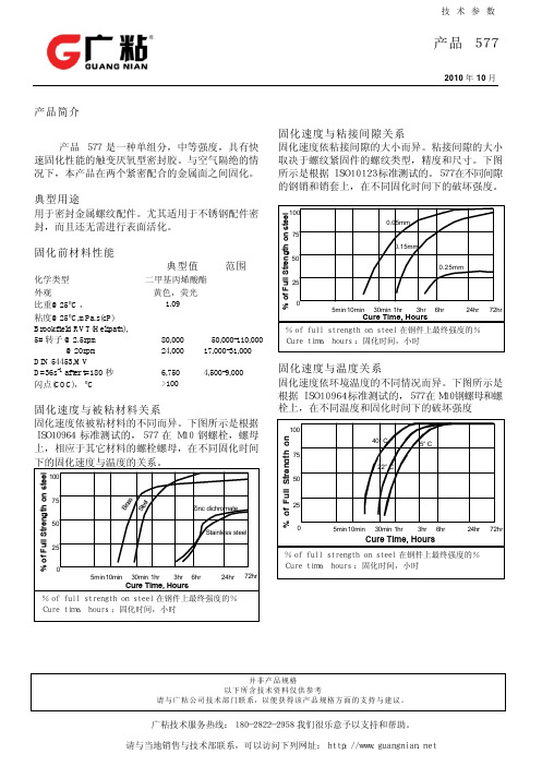
固化速度与活化剂关系 在固化速度太慢或间隙大的 场合,在表面上使用活 化剂可以提高固化速度。下图所示是根据 ISO10964 标准测试的,577 在使用活化剂 N 或 T 的重铬酸锌 钢螺母和螺栓上,在不同固化时间下的破坏强度。
技术参数
产品 577
产品简介
产品 577 是一种单组分,中等强度,具有快
速固化性能的触变厌氧型密封胶。与空气隔绝的情
况下,本产品在两个紧密配合的金属面之间固化。
典型用途
用于密封金属螺纹配件。尤其适用于不锈钢配件密
封,而且还无需进行表面活化。
固化前材料性能
典型值 范围
化学类型
二甲基丙烯酸酯
50 0.25mm
25
% of Full Strength on steel
0
5min 10min 30min 1hr 3hr 6hr
24hr 72hr
Cure Time, Hours
% of full strength on steel 在钢件上最终强度的%
Cure time, hours :固化时间,小时
Cure time, hours :固化时间,小时
固化后材料典型性能
物理性能
热膨胀系数,ASTM D696,K-1
80×10-6
导热系数,ASTM C177,W. m-1 K-1 0.1
比热, kJ.kg-1 K-1
0.3
固化后材料特性
SUP57N20-33_08中文资料
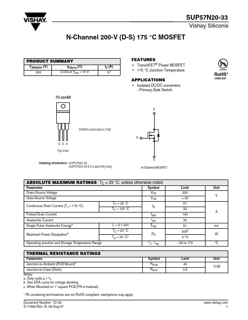
Vishay SiliconixSUP57N20-33N-Channel 200-V (D-S) 175 °C MOSFETFEATURES•TrenchFET ® Power MOSFET •175 °C Junction TemperatureAPPLICATIONS•Isolated DC/DC converters- Primary-Side SwitchPRODUCT SUMMARYV(BR)DSS (V)r DS(on) (Ω)I D (A)2000.033 at V GS = 10 V57Notes:a. Duty cycle ≤ 1 %.b. See SOA curve for voltage derating.c. When Mounted on 1" square PCB (FR-4 material).* Pb containing terminations are not RoHS compliant, exemptions may apply.ABSOLUTE MAXIMUM RATINGS T C = 25°C, unless otherwise notedParameterSymbol Limit Unit Drain-Source Voltage V DS 200VGate-Source VoltageV GS± 20Continuous Drain Current (T J = 175 °C)T C = 25 °C I D 57AT C = 125 °C33Pulsed Drain Current I DM 140Avalanche CurrentI AS35Single Pulse Avalanche Energy a L = 0.1 mH E AS 61mJ Maximum Power DissipationaT C = 25 °C P D 300b W T A = 25 °C c3.75Operating Junction and Storage T emperature RangeT J , T stg- 55 to 175°CTHERMAL RESISTANCE RATINGSParameterSymbol Limit Unit Junction-to-Ambient (PCB Mount)c R thJA 40°C/WJunction-to-Case (Drain)R thJC0.5Vishay SiliconixSUP57N20-33Notes:a. Pulse test; pulse width ≤ 300 µs, duty cycle ≤ 2 %.b. Guaranteed by design, not subject to production testing.c. Independent of operating temperature.Stresses beyond those listed under “Absolute Maximum Ratings” may cause permanent damage to the device. These are stress ratings only, and functional operation of the device at these or any other conditions beyond those indicated in the operational sections of the specifications is not implied. Exposure to absolute maximum rating conditions for extended periods may affect device reliability.SPECIFICATIONS T J = 25°C, unless otherwise notedParameter Symbol Test Conditions Min Typ Max UnitStaticDrain-Source Breakdown Voltage V (BR)DSS V DS = 0 V , I D = 250 µA 200V Gate-Threshold Voltage V GS(th) V DS = V GS , I D = 250 µA 24Gate-Body LeakageI GSS V DS = 0 V, V GS = ± 20 V ± 100nAZero Gate Voltage Drain Current I DSS V DS = 160 V , V GS = 0 V 1µA V DS = 160 V, V GS = 0 V , T J = 125 °C 50V DS = 160 V, V GS = 0 V , T J = 175 °C250On-State Drain Current aI D(on) V DS ≥ 5 V , V GS = 10 V 120A Drain-Source On-State Resistance a r DS(on) V GS = 10 V, I D = 30 A 0.0270.033ΩV GS = 10 V, I D = 30 A, T J = 125 °C 0.069V GS = 10 V, I D = 30 A, T J = 175 °C0.093Forward T ransconductance a g fsV DS = 15 V , I D = 30 A25S Dynamic bInput Capacitance C iss V GS = 0 V , V DS = 25 V , f = 1 MHz5100pFOutput CapacitanceC oss 480Reverse Transfer Capacitance C rss 210Total Gate Charge c Q g V DS = 100 V , V GS = 10 V , ID = 85 A 90130nC Gate-Source Charge c Q gs 23Gate-Drain Charge c Q gd 34Turn-On Delay Time c t d(on) V DD = 100 V, R L = 1.5 Ω I D ≅ 65 A, V GEN = 10 V , R G = 2.5 Ω2435nsRise Time ct r 220330Turn-Off Delay Time c t d(off) 4570Fall Time ct f200300Source-Drain Diode Ratings and Characteristics (T C = 25°C)b Continuous Current I S 65A Pulsed Current I SM 140Forward Voltage a V SD I F = 65 A, V GS = 0 V 1.0 1.5V Reverse Recovery Time t rr I F = 50 A, di/dt = 100 A/µs130200ns Peak Reverse Recovery Current I RM(REC)812A Reverse Recovery ChargeQ rr0.521.2µCOutput CharacteristicsTransfer CharacteristicsVishay SiliconixSUP57N20-33TYPICAL CHARACTERISTICS 25°C, unless otherwise notedAvalanche Current vs. TimeDrain Source Breakdown vs. Junction TemperatureVishay SiliconixSUP57N20-33THERMAL RATINGSVishay Silicon ix main tain s worldwide man ufacturin g capability. Products may be man ufactured at on e of several qualified location s. Reliability data for Silicon Technology and Package Reliability represent a composite of all qualified locations. For related documents such as package/tape drawin gs, part markin g, an d reliability data, see /ppg?72100.Maximum Avalanche and Drain Currentvs. Case TemperatureSafe Operating AreaNormalized Thermal Transient Impedance, Junction-to-CaseDisclaimer Legal Disclaimer NoticeVishayAll product specifications and data are subject to change without notice.Vishay Intertechnology, Inc., its affiliates, agents, and employees, and all persons acting on its or their behalf (collectively, “Vishay”), disclaim any and all liability for any errors, inaccuracies or incompleteness contained herein or in any other disclosure relating to any product.Vishay disclaims any and all liability arising out of the use or application of any product described herein or of any information provided herein to the maximum extent permitted by law. The product specifications do not expand or otherwise modify Vishay’s terms and conditions of purchase, including but not limited to the warranty expressed therein, which apply to these products.No license, express or implied, by estoppel or otherwise, to any intellectual property rights is granted by this document or by any conduct of Vishay.The products shown herein are not designed for use in medical, life-saving, or life-sustaining applications unless otherwise expressly indicated. Customers using or selling Vishay products not expressly indicated for use in such applications do so entirely at their own risk and agree to fully indemnify Vishay for any damages arising or resulting from such use or sale. Please contact authorized Vishay personnel to obtain written terms and conditions regarding products designed for such applications.Product names and markings noted herein may be trademarks of their respective owners.元器件交易网。
SG5772中文资料
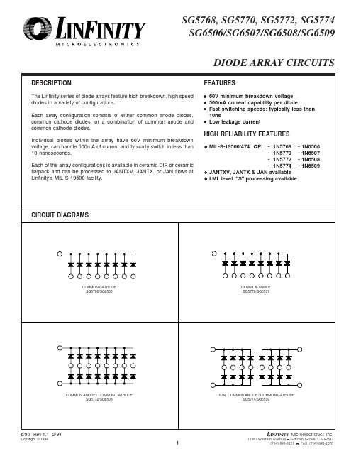
SG5768, SG5770, SG5772, SG5774 SG6506/SG6507/SG6508/SG6509DESCRIPTIONThe Linfinity series of diode arrays feature high breakdown, high speed diodes in a variety of configurations.Each array configuration consists of either common anode diodes, common cathode diodes, or a combination of common anode and common cathode diodes.Individual diodes within the array have 60V minimum breakdown voltage, can handle 500mA of current and typically switch in less than 10 nanoseconds.Each of the array configurations is available in ceramic DIP or ceramic flatpack and can be processed to JANTXV, JANTX, or JAN flows at Linfinity’s MIL-S-19500 facility.DIODE ARRAY CIRCUITS FEATURES•60V minimum breakdown voltage•500mA current capability per diode•Fast switching speeds: typically less than10ns•Low leakage currentHIGH RELIABILITY FEATURES♦MIL-S-19500/474 QPL- 1N5768- 1N6506- 1N5770- 1N6507- 1N5772- 1N6508- 1N5774- 1N6509♦JANTXV, JANTX & JAN available♦LMI level "S" processing availableCIRCUIT DIAGRAMSCOMMON ANODE / COMMON CATHODESG5772/SG6508DUAL COMMON ANODE / COMMON CATHODESG5774/SG6509COMMON CATHODE SG5768/SG6506COMMON ANODE SG5770/SG6507CONNECTION DIAGRAMS & ORDERING INFORMATION (See Notes Below)AmbientTemperature Range Part No.PackageConnection Diagram14-PIN CERAMIC DIP J - PACKAGESG6506J -55°C to 150°C (1N6506)-55°C to 150°CSG5768F -55°C to 150°C (1N5768)-55°C to 150°C10-PIN CERAMIC FLATPACK F - PACKAGESG6507J -55°C to 150°C (1N6507)-55°C to 150°C14-PIN CERAMIC DIP J - PACKAGE1234567141312111098123498567101234567141298111013SG5770F -55°C to 150°C (1N5770)-55°C to 150°CSG6508J -55°C to 150°C (1N6508)-55°C to 150°C14-PIN CERAMIC DIP J - PACKAGESG5772F -55°C to 150°C (1N5772)-55°C to 150°C1234567810912349856710176543214138910111210-PIN CERAMIC FLATPACK F - PACKAGE10-PIN CERAMIC FLATPACK F - PACKAGENote 1. Consult factory for other packages available.2. All packages are viewed from the top.3. Consult factory for JAN, JAN TX, and JAN TXV product availability.CONNECTION DIAGRAMS & ORDERING INFORMATION (continued)AmbientTemperature Range Part No.PackageConnection Diagram14-PIN CERAMIC DIP J - PACKAGESG6509J -55°C to 150°C (1N6509)-55°C to 150°CSG5774F -55°C to 150°C (1N5774)-55°C to 150°C14-PIN CERAMIC FLATPACK F - PACKAGE89101112131417654321489101254376131211。
2N7000中文资料

.590
D
.010
.020
E
.130
.160
G
.010
.104
MM MIN 4.33 4.30 13.97 0.36 3.30 2.44
MAX 4.83 4.83 14.97 0.56 3.96 2.64
NOTE
Revision: 4
1 of 5
2006/05/16
元器件交易网
(
2
25 #6 2#6 2#6
)*+ )
) + )
* )/$ + )
2N7000
MCC TM
Micro Commercial Components
Revision: 4
ቤተ መጻሕፍቲ ባይዱ
2 of 5
2006/05/16
元器件交 易网
2N7000
! " #
$
%
MCC TM
2N7000G中文资料
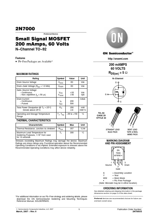
2N7000Preferred DeviceSmall Signal MOSFET200 mAmps, 60 VoltsN−Channel TO−92Features•Pb−Free Packages are Available*MAXIMUM RATINGSRating Symbol Value Unit Drain Source Voltage V DSS60Vdc Drain−Gate Voltage (R GS = 1.0 M W)V DGR60Vdc Gate−Source Voltage− Continuous− Non−repetitive (t p≤ 50 m s)V GSV GSM±20±40VdcVpkDrain Current− Continuous − PulsedI DI DM200500mAdcTotal Power Dissipation @ T C = 25°C Derate above 25°C P D3502.8mWmW/°COperating and Storage TemperatureRangeT J, T stg−55 to +150°C THERMAL CHARACTERISTICSCharacteristic Symbol Max Unit Thermal Resistance, Junction−to−Ambient R q JA357°C/WMaximum Lead Temperature for Soldering Purposes, 1/16″ from case for 10 seconds T L300°CStresses exceeding Maximum Ratings may damage the device. Maximum Ratings are stress ratings only. Functional operation above the Recommended Operating Conditions is not implied. Extended exposure to stresses above the Recommended Operating Conditions may affect device reliability.*For additional information on our Pb−Free strategy and soldering details, please download the ON Semiconductor Soldering and Mounting Techniques Reference Manual, SOLDERRM/D.Preferred devices are recommended choices for future use and best overall value.See detailed ordering and shipping information in the package dimensions section on page 2 of this data sheet.ORDERING INFORMATIONELECTRICAL CHARACTERISTICS(T C = 25°C unless otherwise noted)Characteristic Symbol Min Max Unit OFF CHARACTERISTICSDrain−Source Breakdown Voltage(V GS = 0, I D = 10 m Adc)V(BR)DSS60−VdcZero Gate Voltage Drain Current(V DS = 48 Vdc, V GS = 0)(V DS = 48 Vdc, V GS = 0, T J = 125°C)I DSS−−1.01.0m AdcmAdcGate−Body Leakage Current, Forward(V GSF = 15 Vdc, V DS = 0)I GSSF−−10nAdc ON CHARACTERISTICS (Note 1)Gate Threshold Voltage(V DS = V GS, I D = 1.0 mAdc)V GS(th)0.8 3.0VdcStatic Drain−Source On−Resistance(V GS = 10 Vdc, I D = 0.5 Adc)(V GS = 4.5 Vdc, I D = 75 mAdc)r DS(on)−−5.06.0WDrain−Source On−Voltage(V GS = 10 Vdc, I D = 0.5 Adc)(V GS = 4.5 Vdc, I D = 75 mAdc)V DS(on)−−2.50.45VdcOn−State Drain Current(V GS = 4.5 Vdc, V DS = 10 Vdc)I d(on)75−mAdc Forward Transconductance(V DS = 10 Vdc, I D = 200 mAdc)g fs100−m mhos DYNAMIC CHARACTERISTICSInput Capacitance(V DS = 25 V, V GS = 0,f = 1.0 MHz)C iss−60pFOutput Capacitance C oss−25 Reverse Transfer Capacitance C rss− 5.0 SWITCHING CHARACTERISTICS (Note 1)Turn−On Delay Time(VDD = 15 V, I D = 500 mA,R G = 25 W, R L = 30 W, V gen = 10 V)t on−10nsTurn−Off Delay Time t off−101.Pulse Test: Pulse Width ≤ 300 m s, Duty Cycle ≤2.0%.ORDERING INFORMATIONDevice Package Shipping†2N7000TO−921000 Units / Bulk2N7000G TO−92(Pb−Free)1000 Units / Bulk2N7000RLRA TO−922000 Tape & Reel2N7000RLRAG TO−92(Pb−Free)2000 Tape & Reel2N7000RLRM TO−922000 Tape & Ammo Box2N7000RLRMG TO−92(Pb−Free)2000 Tape & Ammo Box2N7000RLRP TO−922000 Tape & Ammo Box2N7000RLRPG TO−92(Pb−Free)2000 Tape & Ammo Box†For information on tape and reel specifications, including part orientation and tape sizes, please refer to our Tape and Reel Packaging Specifications Brochure, BRD8011/D.I D , D R A I N C U R R E N T (A M P S )r D S (o n ), S T A T I C D R A I N −S O U R C E O N −R E S I S T A N C E (N O R M A L I Z E D )V G S (t h ), T H R E S H O L D V O L T A G E (N O R M A L I Z E D )I D , D R A I N C U R R E N T (A M P S )2.01.81.61.41.21.00.80.60.40.2V DS , DRAIN SOURCE VOLTAGE (VOLTS)Figure 1. Ohmic RegionV GS , GATE SOURCE VOLTAGE (VOLTS)Figure 2. Transfer Characteristics− T, TEMPERATURE (°C)Figure 3. Temperature versus Static Drain−Source On−Resistance T, TEMPERATURE (°C)Figure 4. Temperature versus GateThreshold VoltagePACKAGE DIMENSIONSTO−92 (TO−226)CASE 29−11ISSUE AMNOTES:1.DIMENSIONING AND TOLERANCING PER ANSI Y14.5M, 1982.2.CONTROLLING DIMENSION: INCH.3.CONTOUR OF PACKAGE BEYOND DIMENSION R IS UNCONTROLLED.4.LEAD DIMENSION IS UNCONTROLLED IN P AND BEYOND DIMENSION K MINIMUM.PLANEDIM MIN MAX MIN MAX MILLIMETERSINCHES A 0.1750.205 4.45 5.20B 0.1700.210 4.32 5.33C 0.1250.165 3.18 4.19D 0.0160.0210.4070.533G 0.0450.055 1.15 1.39H 0.0950.105 2.42 2.66J 0.0150.0200.390.50K 0.500−−−12.70−−−L 0.250−−− 6.35−−−N 0.0800.105 2.04 2.66P −−−0.100−−− 2.54R 0.115−−− 2.93−−−V0.135−−−3.43−−−NOTES:1.DIMENSIONING AND TOLERANCING PER ASME Y14.5M, 1994.2.CONTROLLING DIMENSION: MILLIMETERS.3.CONTOUR OF PACKAGE BEYOND DIMENSION R IS UNCONTROLLED.4.LEAD DIMENSION IS UNCONTROLLED IN P AND BEYOND DIMENSION K MINIMUM.DIM MIN MAX MILLIMETERS A 4.45 5.20B 4.32 5.33C 3.18 4.19D 0.400.54G 2.40 2.80J 0.390.50K 12.70−−−N 2.04 2.66P 1.50 4.00R 2.93−−−V3.43−−−STYLE 22:PIN 1.SOURCE2.GATE3.DRAINON Semiconductor and are registered trademarks of Semiconductor Components Industries, LLC (SCILLC). SCILLC reserves the right to make changes without further notice to any products herein. SCILLC makes no warranty, representation or guarantee regarding the suitability of its products for any particular purpose, nor does SCILLC assume any liability arising out of the application or use of any product or circuit, and specifically disclaims any and all liability, including without limitation special, consequential or incidental damages.“Typical” parameters which may be provided in SCILLC data sheets and/or specifications can and do vary in different applications and actual performance may vary over time. All operating parameters, including “Typicals” must be validated for each customer application by customer’s technical experts. SCILLC does not convey any license under its patent rights nor the rights of others. SCILLC products are not designed, intended, or authorized for use as components in systems intended for surgical implant into the body, or other applications intended to support or sustain life, or for any other application in which the failure of the SCILLC product could create a situation where personal injury or death may occur. Should Buyer purchase or use SCILLC products for any such unintended or unauthorized application, Buyer shall indemnify and hold SCILLC and its officers, employees, subsidiaries, affiliates,and distributors harmless against all claims, costs, damages, and expenses, and reasonable attorney fees arising out of, directly or indirectly, any claim of personal injury or death associated with such unintended or unauthorized use, even if such claim alleges that SCILLC was negligent regarding the design or manufacture of the part. SCILLC is an Equal Opportunity/Affirmative Action Employer. This literature is subject to all applicable copyright laws and is not for resale in any manner.PUBLICATION ORDERING INFORMATION。
2SK3567_06中文资料(toshiba)中文数据手册「EasyDatasheet - 矽搜」

25
Qg (nC)
栅源电压
4
2006-11-08
芯片中文手册,看全文,戳
2SK3567
rth – tw
10
1 th (ch-c)
/R
Duty=0.5 0.2
th (t)
0.1
0.1
0.05
阻抗ř 0.02
归一化瞬态热
0.01 0.01
SINGLE PULSE
0.001
10μ
100μ
2SK3567
单位:mm
绝对最大额定值
(Ta = 25°C)
特点
符号
等级
单元
漏源电压
漏极 - 栅极电压(R
栅源电压
GS = 20 kΩ)
漏极电流
漏极功耗(TC
DC (注1)
脉冲(T = 1毫秒) (注1)
= 25°C)
单脉冲雪崩能量
(注2)
雪崩电流
重复雪崩能量(注3)
通道温度
存储温度范围
VDSS VDGR VGSS
10
100
VDS (V)
Vth - 锝
5
4
3
(V)
th 2
V
COMMON SOURCE
1 栅极阈值电压
VDS = 10 V ID = 1 mA
PULSE TEST
0
80
40
0
40
外壳温度
80 120 160
Tc (°C)
PD - 锝
50
40
(W) 30
D
P 20
漏极功耗 10
0
0
40
80
外壳温度
120
X02xxxN中文资料
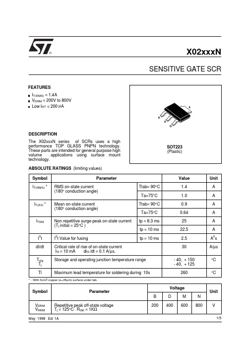
Sensitivity
02
03
05
20
20
200
200
50
0.8
0.1
8 0.5
5
6
1.5
5
200
15
20
15
100
Fig.8 : On-state characteristics (maximum values).
I TSM (A). I2 t (A2 s) 100
ITSM 10
I2 t
1 1
Tj initial = 25oC
tp(ms) 10
I TM (A) 100
Tj initial 25oC
10
Tj max
The ST logo is a trademark of STMicroelectronics
VD=67%VDRM RGK = 1 KΩ
ITM= 3 x IT(AV) VR=35V dI/dt=10A/µs tp=100µs dV/dt=2V/µs VD= 67%VDRM RGK = 1 KΩ
Tj= 25°C MIN MAX
Tj= 25°C MAX Tj= 125°C MIN
Tj= 25°C MIN Tj= 25°C TYP
0.8
= 180o
0.6
0.4
0.2 0.0
0
Ttab (oC) 10 20 30 40 50 60 70 80 90 100 110 120 130
Fig.4 : Relative variation of thermal impedance junction to ambient versus pulse duration.
常用三极管参数大全

玉林万顺达电脑芯片级维修资料 2010-07-20整理玉林万顺达电脑芯片级维修资料 2010-07-20整理玉林万顺达电脑芯片级维修资料 2010-07-20整理玉林万顺达电脑芯片级维修资料 2010-07-20整理玉林万顺达电脑芯片级维修资料 2010-07-20整理玉林万顺达电脑芯片级维修资料 2010-07-20整理玉林万顺达电脑芯片级维修资料 2010-07-20整理玉林万顺达电脑芯片级维修资料 2010-07-20整理玉林万顺达电脑芯片级维修资料 2010-07-20整理玉林万顺达电脑芯片级维修资料 2010-07-20整理玉林万顺达电脑芯片级维修资料 2010-07-20整理玉林万顺达电脑芯片级维修资料 2010-07-20整理玉林万顺达电脑芯片级维修资料 2010-07-20整理玉林万顺达电脑芯片级维修资料 2010-07-20整理玉林万顺达电脑芯片级维修资料 2010-07-20整理玉林万顺达电脑芯片级维修资料 2010-07-20整理玉林万顺达电脑芯片级维修资料 2010-07-20整理玉林万顺达电脑芯片级维修资料 2010-07-20整理玉林万顺达电脑芯片级维修资料 2010-07-20整理玉林万顺达电脑芯片级维修资料 2010-07-20整理玉林万顺达电脑芯片级维修资料 2010-07-20整理玉林万顺达电脑芯片级维修资料 2010-07-20整理玉林万顺达电脑芯片级维修资料 2010-07-20整理玉林万顺达电脑芯片级维修资料 2010-07-20整理玉林万顺达电脑芯片级维修资料 2010-07-20整理玉林万顺达电脑芯片级维修资料 2010-07-20整理玉林万顺达电脑芯片级维修资料 2010-07-20整理玉林万顺达电脑芯片级维修资料 2010-07-20整理玉林万顺达电脑芯片级维修资料 2010-07-20整理玉林万顺达电脑芯片级维修资料 2010-07-20整理。
2N5551中文资料_数据手册_参数

Packing Method Ammo
Tape and Reel Tape and Reel
Bulk Tape and Reel
© 2009 Fairchild Semiconductor Corporation
Top Mark 5551 5551 5551 5551 3S
Package TO-92 3L TO-92 3L TO-92 3L TO-92 3L SOT-23 3L
Note: 1. Suffix “-C” means Center Collector in 2N5551 (1. Emitter 2. Collector 3. Base)
Symbol
Parameter
Value
Units
VCEO VCBO VEBO
IC TJ, Tstg(2)
Collector-Emitter Voltage Collector-Base Voltage Emitter-Base Voltage Collector current - Continuous Junction and Storage Temperature
2N5551 / MMBT5551 Rev. 1.1.0
1
2N5551 / MMBT5551 — NPN General-Purpose Amplifier
Absolute Maximum Ratings(2)
Stresses exceeding the absolute maximum ratings may damage the device. The device may not function or be operable above the recommended operating conditions and stressing the parts to these levels is not recommended. In addition, extended exposure to stresses above the recommended operating conditions may affect device reliability. The absolute maximum ratings are stress ratings only. Values are at TA = 25°C unless otherwise noted.
第13章-功率接口设计

14
晶体管输出型光电耦合器除了可作为开关使用外,还可用作线 性耦合器,在发光二极管上提供一个偏置电流,再把信号电压 通过电阻耦合到发光二极管上,引起其亮度的变化,从而输出 电流也就将随输入的信号电压线性变化。
继电器的动作由单片机的P1.0端控制。P1.0端输出低电平 时,继电器J吸合;P1.0端输出高电平时,继电器J释放。采 用这种控制逻辑可以使继电器在上电复位或单片机受控复位 时不吸合。
继电器J由晶体管9013驱动,9013可以提供300mA的驱动电 流,适用于继电器线圈工作电流小于300mA的场合。Vc的电 压范围是6~30V。光电耦合器使用TIL117。TIL117有较高的 电流传输比,最小值为50%。晶体管9013的电流放大倍
12
13.2.1. 晶体管输出型光电耦合器驱动接口 晶体管输出型光电耦合器作为开关使用,其受光器是光电晶
体管。光电晶体管除了没有使用基极外,跟普通晶体管一样。 取代基极电流的是以光作为晶体管的输入。
当光电耦合器的发光二极管发光时,光电晶体管受光的影响 在cb间和ce间有电流流过,这两个电流基本上受光的照度控制, 常用ce极间的电流作为输出电流,输出电流受Vce的电压影响 很小,在Vce增加时,稍有增加。光电晶体管的集电极电流Ic与 发光二极管的电流IF之比称为光电耦合器的电流传输比。
大电流负载,如电动机、电磁铁、继电器、灯泡等,显然不能 直接用单片机的I/O线来驱动,单片机必须通过各种驱动电路和 开关电路来驱动。此外,为了使单片机与强电隔离和抗干扰, 有时需加接光电耦合器。我们称上述各类接口为单片机的功率 接口。本章将介绍单片机功率接口用到的各种器件以及功率接 口设计。
2N5779和2N5780产品数据表说明书
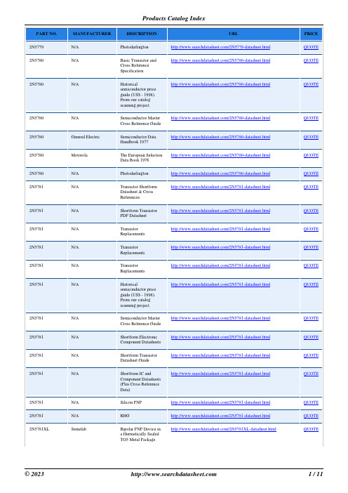
MANUFACTURER
DESCRIPTION
URL
N/A
Photodarlington
/2N5779-datasheet.html
N/A
Basic Transistor and
/2N5780-datasheet.html
N/A
Shortform Electronic
/2N5782-datasheet.html
Component Datasheets
N/A
Shortform Transistor
/2N5782-datasheet.html
N/A
Transistor Shortform
/2N5781-datasheet.html
Datasheet & Cross
References
N/A
Shortform Transistor
/2N5781-datasheet.html
semiconductor price
guide (US$ - 1998).
From our catalog
scanning project.
N/A
Semiconductor Master /2N5782-datasheet.html
Cross Reference Guide
N/A
Shortform Electronic
/2N5781-datasheet.html
Component Datasheets
N/A
Shortform Transistor
/2N5781-datasheet.html
N/A
Transistor Shortform
/2N5783-datasheet.html
2N7002 数据表 .pdf.pdf说明书
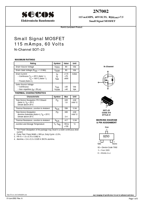
ELECTRICAL CHARACTERISTICS (TA = 25°C unless otherwise noted)
Characteristic
Symbol
Min
OFF CHARACTERISTICS
Drain–Source Breakdown Voltage (VGS = 0, ID = 10 µAdc)
VDSS
VDGR
ID ID IDM
60
60
±ā115 ±ā75 ±ā800
Vdc Vdc mAdc
Gate–Source Voltage – Continuous – Non–repetitive (tp ≤ 50 µs)
THERMAL CHARACTERISTICS
VGS
±ā20
Vdc
VGSM
±ā40
Figure 2. Transfer Characteristics
VGS(th), THRESHOLD VOLTAGE (NORMALIZED)
2.4
2.2 2.0 VGS = 10 V
ID = 200 mA 1.8
1.6
1.4
1.2
1.0
0.8
0.6
0.4 -ā60
-ā20
+ā20
+ā60
+ā100
Turn–On Delay Time Turn–Off Delay Time
(VDD = 25 Vdc, ID ^ 500 mAdc, RG = 25 Ω, RL = 50 Ω, Vgen = 10 V)
BODY–DRAIN DIODE RATINGS
td(on)
–
td(off)
SN75107BD 数据手册说明书
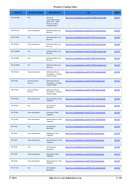
SN75107AJ SN75107BJ SN75108AJ SN75108BD SN75108BJ SN75108BN SN75109AJ
SN75109J
SN75109N
SN7510FA SN7510FA SN7510FA SN7510FA SN7510L SN7510L SN7510L SN7510P SN7510P SN7510P SN7511FA
N/A
IC Datasheets -
/SN7510L-datasheet.html
Shortform
Texas Instruments
Differential Video Amplifier
/SN7510L-datasheet.html
Advanced Micro Devices
Differential DriverTransmitter - ConstantCurrent Output
/SN75109N-datasheet.html
Texas Instruments
General Purpose Video Amplifier
Shortform
Texas Instruments
Differential Video Amplifier
/SN7510P-datasheet.html
Texas Instruments
General Purpose Video Amplifier
Differential Video Amplifier
/SN7510FA-datasheet.html
Texas Instruments
General Purpose Video Amplifier
2N5018中文资料(LINEAR)中文数据手册「EasyDatasheet - 矽搜」
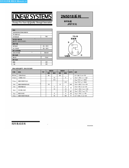
线性集成系统
•
ECN# 2N5018
2N5019 15 75 25 100
UNITS ns
开关电路特性
SYM. VDD VGG RL RG ID(on) VGS(H) VGS(L)
2N5018 -6V 12V 910Ω 220Ω -6mA 0V 12V
2N5019 -6V 8V
1.8KΩ 390Ω -3mA 0V 7V
0.210 0.170
BV GSS V GS(of f )
门源击穿电压 门源截止电压
VDS(on) 漏极至源极导电压
IDSS 漏极至源极饱和电流 IGSS 栅极泄漏电流
ID(off) 排水截止电流
I DGO rDS(on)
漏反向电流 漏极至源极导通电阻
2N5018系列
单P沟道 JFET开关
75Ω
-55〜150℃ -55〜150℃
切换测试电路
V
GG
V
DD
V
GS(H)
V
GS(L)
1.2k 0.1µF
51
1.2k
51
R
L
RG 7.5k
Sampling Scope 51
1. 绝对最大额定值的限制值高于其适用性可能受到损害. 2. 脉冲测试:PW≤为300μs,占空比≤3%
3. 减免为3mW /°C以上25℃.
NOTES
提供的资料由线性集成系统被认为是准确可靠的.但是,没有责任承担其使用;也不对任何侵犯第三方专利或其他权利的可能导致其使用.没有获发牌照以暗 示或以其他方式线性集成系统中的任何专利或专利的权利.
45
45
VDS = -15V, V GS = 0V f = 1MHz
2N7002中文资料_数据手册_参数

件编号:71333 S09-0857-REV. E,2009年5月18日 VISHAY SILICONIX 2N7002K典型征 25°C,除非另有说明源极 - 漏极二极管正向电压温度阈值电 压方差 1.2 1.5 1 100 1000 0.0 0.3 0.6 0.9 T J = 125℃ V SD - 源极至漏极电压(V) 10 T J = - 55℃ V GS = 0V T J = 25℃ - 0.8 - 0.6 - 0.4 - 0.2 0.0 0.2 0.4 - 50 - 25 0 25 50 75 100 125 150 I D = 250μA T J - 结温(°C)导通电阻与栅源电压的关系单脉冲功率,结到环境 0 1 2 3 4五 02468 10 V GS - 栅极 - 源极电压(V) 我 D = 500毫安 我 D = 200毫安 0.01 0 1 2.5 3 100 600 0.1时间(S) 1.5 2 0.5 1 10 T A = 25℃归一化热暂态阻抗,结到环境 10 10 -3 10 -2 1 10 600 10 -1 -4 100 2 1 0.1 0.01 0.2 0.1 0.05 0.02单脉冲占空比= 0.5方波脉冲持续时间(S) 1.工作周期D = 2.每单位基数= R THJA = 350℃/ W 3. T JM - T A = P DM Z THJA(T) T 1 T 2 T 1 T 2笔记: 4.表面安装 P D
万联芯城
万联芯城-电子元器件采购网,专 为终端工厂客户提供一站式电子元器件配套服务,万 联芯城所售电子元器件均为原装现货库存,提交 BOM 表立即报价。万联芯城代理长电,顺络,先科 ST 等知名电子元器件品牌,价格有明显的优势,欢 迎广大客户咨询相关采购业务。点击进入万联芯城。
PHP2N50中文资料

GENERAL DESCRIPTIONQUICK REFERENCE DATAN-channel enhancement mode SYMBOL PARAMETERMAX.UNIT field-effect power transistor in a plastic envelope featuring high V DS Drain-source voltage 500V avalanche energy capability,stable I D Drain current (DC)2A off-state characteristics,fast P totTotal power dissipation50W switching and high thermal cycling R DS(ON)Drain-source on-state resistance5Ωperformance with low thermal resistance.Intended for use in Switched Mode Power Supplies (SMPS),motor control circuits and general purpose switching applications.PINNING - TO220ABPIN CONFIGURATIONSYMBOLLIMITING VALUESLimiting values in accordance with the Absolute Maximum System (IEC 134)SYMBOL PARAMETER CONDITIONSMIN.MAX.UNIT I DContinuous drain current T mb = 25 ˚C; V GS = 10 V -2A T mb = 100 ˚C; V GS = 10 V - 1.3A I DM Pulsed drain current T mb = 25 ˚C -8A P DTotal dissipationT mb = 25 ˚C -50W ∆P D /∆T mb Linear derating factor T mb > 25 ˚C-0.4W/K V GS Gate-source voltage -± 30V E AS Single pulse avalanche V DD ≤ 50 V; starting T j = 25˚C; R GS = 50 Ω;-100mJ energyV GS = 10 VI AS Peak avalanche current V DD ≤ 50 V; starting T j = 25˚C; R GS = 50 Ω;-2A V GS = 10 VT j , T stgOperating junction and - 55150˚Cstorage temperature rangeTHERMAL RESISTANCESSYMBOL PARAMETERCONDITIONSMIN.TYP.MAX.UNIT R th j-mb Thermal resistance junction to -- 2.5K/W mounting baseR th j-aThermal resistance junction to -60-K/WambientELECTRICAL CHARACTERISTICST j = 25 ˚C unless otherwise specified SYMBOL PARAMETERCONDITIONSMIN.TYP.MAX.UNIT V (BR)DSS Drain-source breakdown V GS = 0 V; I D = 0.25 mA 500--V voltage∆V (BR)DSS /Drain-source breakdownV DS = V GS ; I D = 0.25 mA-0.6-V/K ∆T jvoltage temperature coefficient R DS(ON)Drain-source on resistance V GS = 10 V; I D = 1 A - 3.15ΩV GS(TO)Gate threshold voltage V DS = V GS ; I D = 0.25 mA 2.0 3.0 4.0V g fs Forward transconductance V DS = 30 V; I D = 1 A 0.5 1.3-S I DSS Drain-source leakage current V DS = 500 V; V GS = 0 V-125µA V DS = 400 V; V GS = 0 V; T j = 125 ˚C -30250µA I GSS Gate-source leakage current V GS = ±30 V; V DS = 0 V-10200nA Q g(tot)Total gate charge I D = 2 A; V DD = 400 V; V GS = 10 V -2025nC Q gs Gate-source charge-23nC Q gd Gate-drain (Miller) charge -1215nC t d(on)Turn-on delay time V DD = 250 V; I D = 2 A;-10-ns t rTurn-on rise time R G = 24 Ω; R D = 120 Ω-20-ns t d(off)Turn-off delay time -60-ns t f Turn-off fall time -20-ns L d Internal drain inductance Measured from contact screw on - 3.5-nH tab to centre of dieL d Internal drain inductance Measured from drain lead 6 mm - 4.5-nH from package to centre of die L s Internal source inductance Measured from source lead 6 mm -7.5-nH from package to source bond pad C iss Input capacitance V GS = 0 V; V DS = 25 V; f = 1 MHz-236-pF C oss Output capacitance -40-pF C rssFeedback capacitance-22-pFSOURCE-DRAIN DIODE RATINGS AND CHARACTERISTICST j = 25 ˚C unless otherwise specified SYMBOL PARAMETERCONDITIONS MIN.TYP.MAX.UNIT I S Continuous source current T mb = 25˚C --2A (body diode)I SM Pulsed source current (body T mb = 25˚C --8A diode)V SD Diode forward voltage I S = 2 A; V GS = 0 V-- 1.2V t rr Reverse recovery time I S = 2 A; V GS = 0 V; dI/dt = 100 A/µs-300-ns Q rrReverse recovery charge- 2.1-µCMECHANICAL DATANotes1. Observe the general handling precautions for electrostatic-discharge sensitive devices (ESDs) to preventdamage to MOS gate oxide.2. Refer to mounting instructions for TO220 envelopes.3. Epoxy meets UL94 V0 at 1/8".DEFINITIONSData sheet statusObjective specification This data sheet contains target or goal specifications for product development. Preliminary specification This data sheet contains preliminary data; supplementary data may be published later. Product specification This data sheet contains final product specifications.Limiting valuesLimiting values are given in accordance with the Absolute Maximum Rating System (IEC 134). Stress above one or more of the limiting values may cause permanent damage to the device. These are stress ratings only and operation of the device at these or at any other conditions above those given in the Characteristics sections of this specification is not implied. Exposure to limiting values for extended periods may affect device reliability. Application informationWhere application information is given, it is advisory and does not form part of the specification.© Philips Electronics N.V. 1997All rights are reserved. Reproduction in whole or in part is prohibited without the prior written consent of the copyright owner.The information presented in this document does not form part of any quotation or contract, it is believed to be accurate and reliable and may be changed without notice. No liability will be accepted by the publisher for any consequence of its use. Publication thereof does not convey nor imply any license under patent or other industrial or intellectual property rights.LIFE SUPPORT APPLICATIONSThese products are not designed for use in life support appliances, devices or systems where malfunction of these products can be reasonably expected to result in personal injury. Philips customers using or selling these products for use in such applications do so at their own risk and agree to fully indemnify Philips for any damages resulting from such improper use or sale.。
SA577N资料

Product specification
Unity gain level programmable low power compandor
NE/SA577
TYPICAL PERFORMANCE CHARACTERISTICS
VCC = 3.6V, TA = 25°C, R1=R3=7.15kΩ, R2=100kΩ, 0dB level = 100mV, Freq. = 1kHz SUPPLY CURRENT vs SUPPLY VOLTAGE
0.4
EXPANDOR 0.2 UNITY GAIN ERROR (dB)
0.2 UNITY GAIN ERROR (dB)
0 COMPRESSOR
0 COMPRESSOR
-0.2
-0.2
-0.4
-0.4
-0.6 2 3 4 5 SUPPLY VOLTAGE (V) 6 7
-0.6 -40 -20 0 20 40 60 TEMPERATURE (°C) 80 100
(1.4mA @ 3.6V)
VREF 5 IREF GND 6 7
• 0dB level programmable • Over 90dB of dynamic range • Wide input/output swing capability
(rail-to-rail) (10mVRMS to 1.0VRMS)
元器件交易网
Philips Semiconductors RF Communications Products
Product specification
Unity gain level programmable low power compandor
- 1、下载文档前请自行甄别文档内容的完整性,平台不提供额外的编辑、内容补充、找答案等附加服务。
- 2、"仅部分预览"的文档,不可在线预览部分如存在完整性等问题,可反馈申请退款(可完整预览的文档不适用该条件!)。
- 3、如文档侵犯您的权益,请联系客服反馈,我们会尽快为您处理(人工客服工作时间:9:00-18:30)。
Customized Label
(TO-92) BULK PACKING INFORMATION
EOL CODE J18Z J05Z NO EOL CODE DESCRIPTION TO-18 OPTION STD TO-5 OPTION STD TO-92 STANDARD STRAIGHT FOR: PKG 92, 94 (NON PROELECTRON SERIES), 96 TO-92 STANDARD STRAIGHT FOR: PKG 94 (PROELECTRON SERIES BCXXX, BFXXX, BSRXXX), 97, 98 LEADCLIP DIMENSION NO LEAD CLIP NO LEAD CLIP NO LEADCLIP QUANTITY 2.0 K / BOX 1.5 K / BOX 2.0 K / BOX
Thermal Characteristics
Symbol
PD RθJC RθJA
TA = 25°C unless otherwise noted
Characteristic
Total Device Dissipation Derate above 25°C Thermal Resistance, Junction to Case Thermal Resistance, Junction to Ambient
SMALL SIGNAL CHARACTERISTICS
NF Ccb Cib hfe Noise Figure Collector-Base Capacitance Input Capacitance Small-Signal Current Gain IC = 1.0 mA, VCE = 8.0 V, f = 60 MHz, Rg = 400 Ω VCB = 10 V, IE = 0, f = 1.0 MHz VEB = 0.5 V IC = 8.0 mA, VCE = 10 V, f = 100 MHz IC = 8.0 mA, VCE = 10 V, f = 1.0 kHz IE = 8.0 mA, VCB = 10 V, f = 79.8 MHz 9.0 40 3.0 6.0 0.7 1.1 2.0 18 240 20 dB pF pF
元器件交易网
2N5770
Discrete POWER & Signal Technologies
2N5770
C
BE
TO-92
NPN RF Transistor
This device is designed for use as RF amplifiers, oscillators and multipliers with collector currents in the 1.0 mA to 30 mA range. Sourced from Process 43. See PN918 for characteristics.
ORDER STYLE D74Z (M)
ORDER STYLE D75Z (P)
FIRST WIRE OFF IS EMITTER (ON PKG. 92) ADHESIVE TAPE IS ON BOTTOM SIDE FLAT OF TRANSISTOR IS ON BOTTOM
FIRST WIRE OFF IS COLLECTOR (ON PKG. 92) ADHESIVE TAPE IS ON BOTTOM SIDE FLAT OF TRANSISTOR IS ON TOP
BULK OPTION
See Bulk Packing Information table Anti-static Bubble Sheets
FSCINT Label
L34Z
NO LEADCLIP
2.0 K / BOX
2000 units per EO70 box for std option
114mm x 102mm x 51mm Immediate Box
Machine Option “A” (H) Machine Option “E” (J)
Style “A”, D26Z, D70Z (s/h)
Style “E”, D27Z, D71Z (s/h)
TO-92 Radial Ammo Packaging Configuration: Figure 3.0
FIRST WIRE OFF IS COLLECTOR ADHESIVE TAPE IS ON THE TOP SIDE FLAT OF TRANSISTOR IS ON TOP FIRST WIRE OFF IS EMITTER ADHESIVE TAPE IS ON THE TOP SIDE FLAT OF TRANSISTOR IS ON BOTTOM
Absolute Maximum Ratings*
Symbol
VCEO VCBO VEBO IC TJ, Tstg Collector-Emitter Voltage Collector-Base Voltage Emitter-Base Voltage Collector Current - Continuous
Max
2N5770 350 2.8 125 357
Units
mW mW/ °C °C/W °C/W
© 1997 Fairchild Semiconductor Corporation
元器件交易网
2N5770
NPN RF Transistor
(continued)
Electrical Characteristics
5 EO70 boxes per intermediate Box 530mm x 130mm x 83mm Intermediate box Customized Label
FSCINT Label 10,000 units maximum per intermediate box for std option
ON CHARACTERISTICS*
hFE VCE( sat) VBE( sat) DC Current Gain Collector-Emitter Saturation Voltage Base-Emitter Saturation Voltage VCE = 1.0 V, IC = 3.0 mA VCE = 10 V, IC = 8.0 mA IC = 10 mA, IB = 1.0 mA IC = 10 mA, IB = 1.0 mA 20 50 200 0.4 1.0 V V
NOTES: 1) These ratings are based on a maximum junction temperature of 150 degrees C. 2) These are steady state limits. The factory should be consulted on applications involving pulsed or low duty cycle operations.
SPEC REV: QA REV:
B2
FSCINT Label
(FSCINT)
5 Reels per Intermediate Box F63TNR Label Customized Label 375mm x 267mm x 375mm Intermediate Box
F63TNR Label sample
Packing Reel Style A E Ammo M P Quantity 2,000 2,000 2,000 2,000 EOL code D26Z D27Z D74Z D75Z
AMMO PACK OPTION
See Fig 3.0 for 2 Ammo Pack Options
Unit weight = 0.22 gm Reel weight with components = 1.04 kg Ammo weight with components = 1.02 kg Max quantity per intermediate box = 10,000 units
FSCINT Label 327mm x 158mm x 135mm Immediate Box Customized Label 5 Ammo boxes per Intermediate Box F63TNR Label 333mm x 231mm x 183mm Intermediate Box
©2001 Fairchild Semiconductor Corporation
March 2001, Rev. B1
元器件交易网
TO-92 Tape and Reel Data, continued
TO-92 Reeling Style Configuration: Figure 2.0
Symbol Parameter
TA = 25°C unless otherwise noted
Test Conditions
Min
Max
Units
OFF CHARACTERISTICS
V(BR)CEO V(BR)CBO V(BR)EBO ICBO IEBO Collector-Emitter Breakdown Voltage* Collector-Base Breakdown Voltage Emitter-Base Breakdown Voltage Collector Cutoff Current Emitter Cutoff Current IC = 3.0 mA, IB = 0 IC = 1.0 µA, IE = 0 IE = 10 µA, IC = 0 VCB = 15 V, IE = 0 VCB = 15 V, IE = 0, TA = 150 °C VEB = 3.0 V, IC = 0 VEB = 2.0 V, IC = 0 15 30 4.5 10 1.0 10 1.0 V V V nA µA µA µA
