三泰电子VTM DM单
VITSON产品说明书中文英文

深圳市慧拓鑫科技有限公司Shenzhen Hui Tuo Xin Technology Co., Ltd.产品资料Product information1、TOP电源防雷箱系列(TOP Power lightning protection box series) (1)2、TP 限压型电源防雷模块系列(TP Voltage limiting type power supply lightning protection module series) (8)3、TP直流电源防雷模块系列(TP DC power supply lightning protection module series) (14)4、TCP电源未端精细防护防雷器系列(TCP Power supply terminal fine protective lightning arrester series) (20)5、TDC 电源插座(TDC Power supply lightning protection socket series) (25)6、TV 视频防雷器系列(TV Video arrester series) (30)7、T 视频/射频防雷器系列(T Video / RF lightning arrester series) (36)8、TC控制线路防雷器系列( TC Control circuit lightning arrester series) (40)9、10/100M网络线路防雷器(10/100M Network circuit lightning arrester) (44)10、通讯专线防雷器(Communication line lightning arrester) (49)11、TT天馈线路防雷器系列(TT Antenna line arrester series) (53)1、TOP电源防雷箱系列(TOP Power lightning protection box series)产品介绍Product introductionTOP电源防雷箱系列依据IEC标准设计,8/20波形最大通流容量20KA-100KA,能对电源系统的浪涌电压进行有效的钳制,电源B、C、D级产品均具备。
三泰电子柜面清

柜面清
成都三泰电子研发中心 “ST-CST柜面清”是为了实现业务流程中的信息交互功能而诞生,设备在实现信息交互的需求外,还集成了密码键盘、评价器、对讲机、员工牌,并将屏幕保护功能扩展成广告功能。
通过使用“ST-CST柜面清”整合密码键盘、信息交互、满意度评价及广告等多项功能,有效简化应用,提高安全防控能力,促进产品宣传推广,提高企业形象。
同时还大大减少空间占用,有效美化办公环境。
产品具有以下特点:
●外观设计:符合人体工程学设计原理,具备防窥、防爆功能。
●安全可靠:底层采用定制的LINUX系统,去除了不必要的组件,增加了系统和应用
程序的稳定性。
●安装方便:通过RS232与终端连接,外接5V电源,安全可靠。
●管理方便:通过USB接口可实现统一广告图片更新、管理。
●升级方便:通过特定升级包可对用户的特殊需求制作相应版本进行升级。
●扩展性强:设备预留常用接口,以适应客户特殊需求。
贴片元件大全

05 05 05 05 05 05 05 -05 050 050 05F 05F 05L 05NU 05s 06 06 06 06 06 06 06 06 06 06 06 06 -06 -06 065 066 066 067 06F 07 07 07 07 07 07 07 07 07 -07 071 074 07N60S5 07N60S5 08 08 08 08 08 08 08 08
TK17020M SPB02N60S5 SPD02N60S5 SPN02N60S5 TK70002M DTC143TE DTC143TKA DTC143TUA Gali-3 JDP2S05CT MAR-3SM PDTA114EE PDTA114EE PDTA114EEF PDTA114EK PDTA114EK RAM-3 VAM-3 00 BZG03-C10 BZG03-C110 BZG03-C11 BZG03-C120 BZG03-C12 BZG03-C130 BZG03-C13 BZG03-C150 BZG03-C15 BZG03-C160 BZG03-C16 BZG03-C180 BZG03-C18 BZG03-C200 BZG03-C20 BZG03-C220 BZG03-C22 BZG03-C240 BZG03-C24 BZG03-C270 BZG03-C27 BZG03-C30 BZG03-C33 BZG03-C36 BZG03-C39 BZG03-C43 BZG03-C47 BZG03-C51 BZG03-C56 BZG03-C62 BZG03-C68 BZG03-C75 BZG03-C82 BZG03-C91
Manufacturer
Infineon WJC WJC WJC WJC WJC WJC WJC WJC Toshiba Toshiba Toshiba Toshiba Toshiba NEC Hitachi Toshiba Toko Toko Toko Siliconix MCL MiniCircuits MCL MiniCircuits Philips Philips Philips Philips MCL MiniCircuits Philips SGS Siliconix-Vishay SGS Toko Toko Infineon Infineon Infineon Toko Philips Philips Philips Motorola Rohm MCL MiniCircuits Toshiba MCL MiniCircuits Motorola Philips Philips Philips Philips MCL MiniCircuits Philips Siliconix
赛米控丹佛斯 SEMITRANS 全碳化硅功率模块 SKM260MB170SCH17 数据表
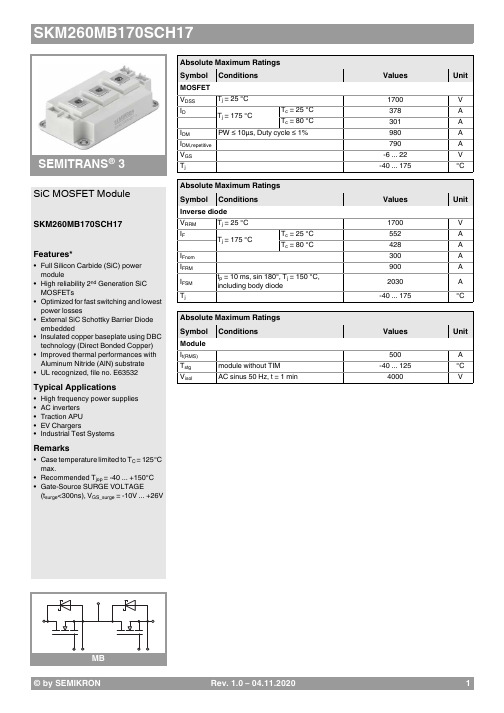
© by SEMIKRONRev. 1.0–04.11.20201SEMITRANS ®3SiC MOSFET ModuleSKM260MB170SCH17Features*•Full Silicon Carbide (SiC) power module•High reliability 2nd Generation SiC MOSFETs•Optimized for fast switching and lowest power losses•External SiC Schottky Barrier Diode embedded•Insulated copper baseplate using DBC technology (Direct Bonded Copper)•Improved thermal performances with Aluminum Nitride (AlN) substrate •UL recognized, file no. E63532Typical Applications•High frequency power supplies •AC inverters •Traction APU •EV Chargers•Industrial Test SystemsRemarks•Case temperature limited to T C = 125°C max.•Recommended T jop = -40 ... +150°C •Gate-Source SURGE VOLTAGE(t surge <300ns), V GS_surge = -10V ... +26VAbsolute Maximum Ratings SymbolConditions Values UnitMOSFET V DSS T j =25°C 1700VI D T j =175°CT c =25°C 378 A T c =80°C301 A I DMPW ≤ 10µs, Duty cycle ≤ 1%980A I DM,repetitive790A V GS -6...22V T j-40 (175)°CAbsolute Maximum Ratings SymbolConditionsValuesUnitInverse diodeV RRM T j =25°C 1700V I F T j =175°CT c =25°C 552A T c =80°C428A I Fnom 300A I FRM 900A I FSM t p =10ms, sin 180°, T j =150°C, including body diode2030A T j-40 (175)°CAbsolute Maximum Ratings SymbolConditions Values UnitModule I t(RMS)500A T stg module without TIM -40...125°C V isolAC sinus 50 Hz, t =1min4000V2Rev. 1.0–04.11.2020© by SEMIKRONSEMITRANS ®3SiC MOSFET ModuleSKM260MB170SCH17Features*•Full Silicon Carbide (SiC) power module•High reliability 2nd Generation SiC MOSFETs•Optimized for fast switching and lowest power losses•External SiC Schottky Barrier Diode embedded•Insulated copper baseplate using DBC technology (Direct Bonded Copper)•Improved thermal performances with Aluminum Nitride (AlN) substrate •UL recognized, file no. E63532Typical Applications•High frequency power supplies •AC inverters •Traction APU •EV Chargers•Industrial Test SystemsRemarks•Case temperature limited to T C = 125°C max.•Recommended T jop = -40 ... +150°C •Gate-Source SURGE VOLTAGE(t surge <300ns), V GS_surge = -10V ... +26VMOSFET V (BR)DSS V GS =0V,I D =1mA, T j =25°C 1700V V GS(th)V DS =V GS , I D =57.75mA1.62.84V I DSS V GS =0V,V DS =1700V, T j =25°C 1.8mA I GSS V GS =22V,V DS =0V 700nA R DS(on)V GS =18V I D =161AchiplevelT j =25°C 8.110m ΩT j =150°C 14m ΩC iss V GS =0V V DS =800Vf =1MHzT j =25°C 27nF C oss T j =25°C 0.88nF C rss T j =25°C0.105nF R Gint T j =25°C2.1ΩQ G V DD =1000V, V GS =-5 ... 20V, I D =300A 1470nC t d(on)V DD =900V I D =300A V GS =-5 / +20VR Gon =0.7ΩR Goff =0.7Ωdi/dt on =12kA/µs di/dt off =9.5kA/µsdv/dt off =22kV/µs T j =150°C 64ns t r T j =150°C 60ns t d(off)T j =150°C162ns t f T j =150°C 32ns E on T j =150°C 7.59mJ E off T j =150°C6.21mJ R th(j-c)per MOSFET0.065K/W R th(c-s)per MOSFET (λgrease =0.81 W/(m*K))0.03K/WCharacteristics SymbolConditionsmin.typ.max.UnitInverse diodeV F = V SD I F =300A chiplevel T j =25°C 1.65 1.95V T j =150°C 2.51 2.86V V F0chiplevel T j =25°C 1.00 1.10V T j =150°C 0.860.96V r F chiplevelT j =25°C2.2 2.8m ΩT j =150°C5.56.3m ΩC j parallel to C oss , f =1MHz, V R =1700V, T j =25°C1.026nF Q c V R =800V, di/dt off =500A/µs, T j =25°C 0.95µCR th(j-c)per diode0.056K/W R th(c-s)per diode (λgrease =0.81 W/(m*K))0.027K/W© by SEMIKRONRev. 1.0–04.11.20203SEMITRANS ®3SiC MOSFET ModuleSKM260MB170SCH17Features*•Full Silicon Carbide (SiC) power module•High reliability 2nd Generation SiC MOSFETs•Optimized for fast switching and lowest power losses•External SiC Schottky Barrier Diode embedded•Insulated copper baseplate using DBC technology (Direct Bonded Copper)•Improved thermal performances with Aluminum Nitride (AlN) substrate •UL recognized, file no. E63532Typical Applications•High frequency power supplies •AC inverters •Traction APU •EV Chargers•Industrial Test SystemsRemarks•Case temperature limited to T C = 125°C max.•Recommended T jop = -40 ... +150°C •Gate-Source SURGE VOLTAGE(t surge <300ns), V GS_surge = -10V ... +26VModule L DS 15nH R DD'+SS'measured per switchT C =25°C0.55m ΩT C =125°C0.85m ΩR th(c-s)1calculated without thermal coupling (λgrease =0.81 W/(m*K))0.008K/W R th(c-s)2including thermal coupling, T s underneath module (λgrease =0.81 W/(m*K))0.013K/W M s to heat sink M635Nm M tto terminals M62.55Nm Nmw325g4Rev. 1.0–04.11.2020© by SEMIKRON© by SEMIKRON Rev. 1.0–04.11.202056Rev. 1.0–04.11.2020© by SEMIKRON© by SEMIKRON Rev. 1.0–04.11.20207This is an electrostatic discharge sensitive device (ESDS) due to international standard IEC 61340.*IMPORTANT INFORMATION AND WARNINGSThe specifications of SEMIKRON products may not be considered as guarantee or assurance of product characteristics ("Beschaffenheitsgarantie"). The specifications of SEMIKRON products describe only the usual characteristics of products to be expected in typical applications, which may still vary depending on the specific application. Therefore, products must be tested for the respective application in advance. Application adjustments may be necessary. The user of SEMIKRON products is responsible for the safety of their applications embedding SEMIKRON products and must take adequate safety measures to prevent the applications from causing a physical injury, fire or other problem if any of SEMIKRON products become faulty. The user is responsible to make sure that the application design is compliant with all applicable laws, regulations, norms and standards. Except as otherwise explicitly approved by SEMIKRON in a written document signed by authorized representatives of SEMIKRON, SEMIKRON products may not be used in any applications where a failure of the product or any consequences of the use thereof can reasonably be expected to result in personal injury. No representation or warranty is given and no liability is assumed with respect to the accuracy, completeness and/or use of any information herein, including without limitation, warranties of non-infringement of intellectual property rights of any third party. SEMIKRON does not assume any liability arising out of the applications or use of any product; neither does it convey any license under its patent rights, copyrights, trade secrets or other intellectual property rights, nor the rights of others. SEMIKRON makes no representation or warranty of non-infringement or alleged non-infringement of intellectual property rights of any third party which may arise from applications. Due to technical requirements our products may contain dangerous substances. For information on the types in question please contact the nearest SEMIKRON sales office. This document supersedes and replaces all information previously supplied and may be superseded by updates. SEMIKRON reserves the right to make changes.8。
3M-Littmann-Stethoscopes公司代理产品目录
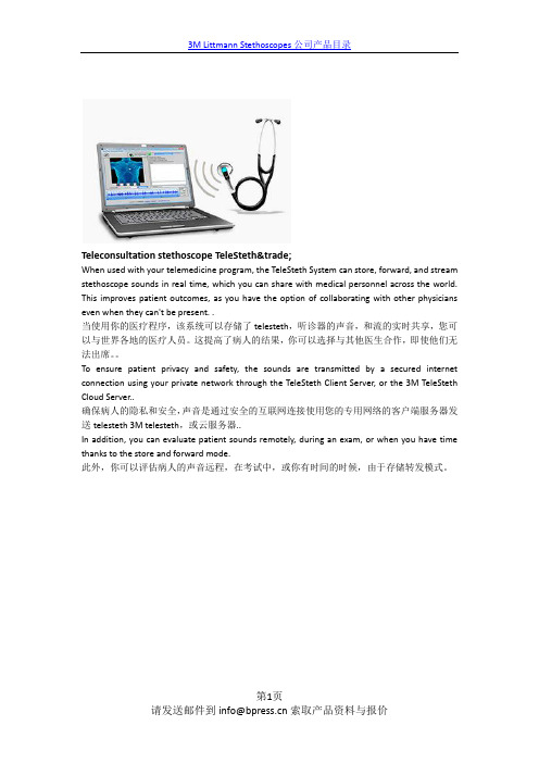
Teleconsultation stethoscope TeleSteth™When used with your telemedicine program, the TeleSteth System can store, forward, and stream stethoscope sounds in real time, which you can share with medical personnel across the world. This improves patient outcomes, as you have the option of collaborating with other physicians even when they can't be present. .当使用你的医疗程序,该系统可以存储了telesteth,听诊器的声音,和流的实时共享,您可以与世界各地的医疗人员。
这提高了病人的结果,你可以选择与其他医生合作,即使他们无法出席。
To ensure patient privacy and safety, the sounds are transmitted by a secured internet connection using your private network through the TeleSteth Client Server, or the 3M TeleSteth Cloud Server..确保病人的隐私和安全,声音是通过安全的互联网连接使用您的专用网络的客户端服务器发送telesteth 3M telesteth,或云服务器..In addition, you can evaluate patient sounds remotely, during an exam, or when you have time thanks to the store and forward mode.此外,你可以评估病人的声音远程,在考试中,或你有时间的时候,由于存储转发模式。
LT6550资料
The q denotes the specifications which apply over the specified temperature range, otherwise specifications are at TA = 25°C. VCC = 3.3V, VGND = 0V; VIN = 0.75V LT6550 (Pins 1,2,3); LT6551 (Pins 1,2,3,4). VEE = 0V LT6550 (Pin 5), unless otherwise noted.
100
300 12 8
q q
1.9 1.9 1.85 10 60 90 3.0 2.5 2.0 3.2 2.9 2.5
2.1 2.1 2.15 30 150 200
V/V V/V V/V mV mV mV V V V
65501f
q q q q q
元器件交易网
LT6550/LT6551
Total Supply Voltage LT6550 (VCC TO VEE) ........................................ 12.6V LT6551 (VCC TO GND) ...................................... 12.6V Input Current (Note 9) ........................................ ±10mA Output Short-Circuit Duration (Note 2) ............ Indefinite Operating Temperature Range ................ – 40°C to 85°C
江苏长江电子科技有限公司 SOT-363 胶合体 MOSFET 产品说明书
JIANGSU CHANGJIANG ELECTRONICS TECHNOLOGY CO., LTDSOT-363 Plastic-Encapsulate MOSFETs2N7002DW Dual N -channel MOSFETFEATUREAPPLICATIONMARKINGMAXIMUM RATINGS (T a =25℃ unless otherwise noted)SOT-363V(BR)DSSR DS(on)MAXI D60V5Ω@10V115m A7Ω@5VEquivalent CircuitSymbol Parameter Value Unit V G S Gate -Source voltage 20 V I D Drain Current 115 mA P D Power Dissipation150 mW R ӨJA 833 ℃/W T J Junction T emperature 150 ℃ T stgStorage T emperature-55-150℃Thermal Resistance from Junction to AmbientV DSDrain-Source voltage60Vz High density cell design for low R DS(ON) Load Switch for Portable Devices z Voltage controlled small signal switch DC/DC Converterz Rugged and reliablezHigh saturation current capabilityz zMOSFET ELECTRICAL CHARACTERISTICSaT =25℃ unless otherwise specifiedParameter SymbolTest conditions M inT yp Max UnitDrain-s ource b reakdown v oltage V (BR)DSS V GS =0 V, I D =250 µA60 Gate-t hreshold v oltage *V th (GS) V DS =V GS , I D =250 µA 1 1.6 2.5 VGate-body l eakagel GSS V DS =0 V, V GS =±20 V±80 nA Zero g ate v oltage d rain c urrentI DSSV DS =60 V, V GS =0 V80nAV GS =10 V, I D =500mA 1.1 5Drain-s ource o n-r esistance * R DS(o n)V GS =5 V, I D =50mA 1.2 7 Ω Forward t ransconductance *g fs V DS =10 V, I D =200mA 80 msV GS =10V, I D =500mA 0.5 3.75 V Drain-source on-voltage *V DS(on)V GS =5V, I D =50mA 0.375 V Diode f orward v oltageV SDI S =115mA, V GS =0 V0.551.2VInput c apacitance C iss 50Output c apacitance C oss 25 Reverse t ransfer c apacitanceC r ss V DS =25V, V GS =0V, f=1MHz 5pF SWITCHING TIMETurn-on t ime t d(on) 20 Turn-off t ime t d(off) V DD =25 V, R L =50ΩI D =500mA,V GEN =10V,G =25 Ω 40ns* Pulse Test: Pulse width ≤300µs,duty cycle ≤2%.** These parameters have no way to verify.** **** ** **0.00.20.40.60.8 1.0 1.2 1.4 1.60.010.11255075100125V SDI S ——S O U R C E C U R R E N T I S (A )SOURCE TO DRAIN VOLTAGE V SD (V)DRAIN CURRENT I D (A)GATE TO SOURCE VOLTAGE V GS (V)Threshold VoltageT H R E S H O L D V O L T A G E V T H (V )JUNCTION TEMPERATURE T j ()℃SO T -363 Package Outline DimensionsSO T -363Suggested Pad LayoutSO T-363 Tape and Reel。
名厂IC代理商

新昕科技(Serial)
/cn/
科通数字技术部
17 XILINX,赛灵斯
Digi-Key 公司
800-344-4539
18 MICROCHIP(美国微芯) 深圳市英锐恩科技有限公司
安拓电子技术有限公司
/
上海京西电子信息系统有限公司 (深圳代表处)
深圳环捷电子有限公司
北京明新视讯科技有限公司深圳办事处
增你强(深圳)科技有限公司
15 IR
威健实业国际有限公司(文晔)
领科商贸(深圳)有限公司深圳分公司(文晔)
富ห้องสมุดไป่ตู้电子(香港)有限公司
世平集团 深圳代表处 中國深圳市僑城東路華僑城東部工業區東H1棟四樓 曾文坤 86-755-26711655-7507 86-755-26711655-7231 86-755-26957066
世健国际贸易(深圳)有限公司 深圳市深南东路4003号世界金融中心A座21楼A室 张婷婷 ariel.xu@ emily.zhang@ 518008 86-755-83640166-883 86-755-83640166-651 86-755-25982255
NTC-1%热敏电阻DATA SHEET
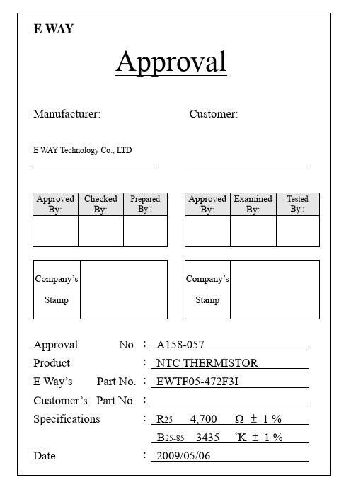
ACCESSORY : RESISTANCE-TEMPERATURE CHARACTERISTICS
10-5
Resistance-Temperature Characteristics
Part No. : EWTF05-472F3I R: B: 4,700 3435 ohms °K ± ± 1% 1%
*Maximum Power Rating = Thermal Dissipation Constant × (125℃-25℃)
10-2
RELIABILITY TEST
PERFORMANCE Life Humidity Thermal Shock Solderability TEST METHOD
ORDERING INFORMATION EWTF
1 ○
05 472
2 ○ 3 ○
F
4 ○
3I
5 ○
1. Series E-Way SMD Thermistor. (TH - Lead (Pb) ; TF - Lead Free ) 2. Dimension : 06 ( 1206 ) , 05 ( 0805 ) , 03 ( 0603 ) , 02 ( 0402 ) 3. Resistance : 472 = 47 x 102 = 4,700 ohm 4. R Tolerance : F:±1% ; G:±2% ; H:±3% ; J:±5% ; K:±10% 5. B value : 1: 1000 2: 2000 3: 3000 4: 4000 A: 0~50 B: 51~100 C: 101~150 D: 151~200 E: 201~250 F: 251~300 G: 301~350 H: 351~400 I: 401~450 J: 451~500 K: 501~550 L: 551~600 M: 601~650 N: 651~700 O: 701~750 P: 751~800 Q: 801~850 R: 851~900 S: 901~950 T: 951~999
润湿剂Terwet1004MSDS

Material Safety Data SheetProduct name: TERWET ® 1004 Substance Key: 000000005548 Issued: 01.03.2006 Version: 3.0 Page: 1 of 61. IDENTIFICATION OF THE MATERIAL AND SUPPLIERProduct name: TERWET ® 1004TERWET is a registered trademark of Huntsman Corporation or an affiliate thereof in one or more, but not all, countries.Other names:Recommended use: Agricultural wetting agent.Supplier: Huntsman Corporation Australia Pty LimitedACN: 083 984 187ABN: 67 083 984 187Street address: 61 Market RoadBrooklyn Victoria 3012AustraliaTelephone: +613 9316 3646Facsimile: +613 9316 3647Emergency telephone number: Australia: 1800 786 152 (ALL HOURS)International: + 65 6336 6011 (ALL HOURS)2. HAZARDS IDENTIFICATIONHazard classificationHazardous Substance. Non-dangerous goods.This material is classified as hazardous according to health criteria of NOHSC Australia.Not classified as Dangerous Goods by the criteria of the Australian Dangerous Goods Code (ADG Code) for transport by Road and Rail.Hazard categoryXi IrritantRisk phrase(s)R38 Irritating to skin.R41 Risk of serious eye damage.Safety phrase(s)S24/25 Avoid contact with skin and eyes.S26 In case of contact with eyes, rinse immediately with plenty of water and seek medicaladvice.S36/37/39 Wear suitable protective clothing, gloves and eye/face protection.Poisons schedule (Aust): None Allocated3. COMPOSITION/INFORMATION ON INGREDIENTSMaterial Safety Data SheetProduct name: TERWET ® 1004 Substance Key: 000000005548 Issued: 01.03.2006 Version: 3.0 Page: 2 of 6Appearance: Free-flowing off-white powder.-------------------------------------------------------------------------------------------------------------------------CHEMICAL ENTITY CAS NO. PROPORTION -------------------------------------------------------------------------------------------------------------------------Anionic surfactant - VHIGHSodium sulphate 7757-82-6 LOWSodium chloride 7647-14-5 LOW-------100 %PROPORTIONS (% weight per weight)VHIGH > 60, HIGH 30 - 60, MED 10 - 29, LOW 1 - 9, VLOW < 1All the constituents of this material are listed on the Australian Inventory of Chemical Substances (AICS).4. FIRST AID MEASURESIngestion: Rinse mouth with water. Give plenty of water to drink. If vomiting occurs give further water. Seek medical advice.Eye contact: If in eyes, hold eyelids apart and flush continuously with running water. Continue flushing until advised to stop by the Poisons Information Centre or a doctor, or for at least 15 minutes. Transport to hospital or medical centre.Skin contact: If skin or hair contact occurs, remove contaminated clothing and flush skin and hair with running water. If irritation occurs seek medical attention. Wash contaminated clothing before re-use.Inhalation: Remove victim from exposure. Keep at rest until fully recovered. Seek medical advice.Medical attention and special treatment: Treat symptomatically. Can cause corneal burns.5. FIRE-FIGHTING MEASURESSuitable extinguishing media: For large fires use water fog, fine water spray or foam. Do not use water jets. For small fires use foam, dry chemical, carbon dioxide or water spray.Hazards from combustion products: Combustible solid. On burning will emit toxic fumes including those of oxides of carbon and sulphur.Precautions for fire fighters and special protective equipment: Fire fighters to wear self-contained breathing apparatus if risk of exposure to vapour or products of combustion as well as structural fire fighters uniform.Hazchem code: None assigned.6. ACCIDENTAL RELEASE MEASURESEmergency procedures: Avoid accidents, clean up immediately. Wear protective equipment to prevent skin and eye contamination and inhalation of dust. Do not touch or walk through spilled material.Material Safety Data SheetProduct name: TERWET ® 1004 Substance Key: 000000005548 Issued: 01.03.2006 Version: 3.0 Page: 3 of 6Methods and materials for containment and clean up procedures: Contain – prevent contamination of drains and waterways. Cover with damp absorbent (inert material, sand or soil). Sweep up, but avoid generating dust. Collect and seal in properly labelled drums for disposal. Wash area down with excess water to remove residual material.7. HANDLING AND STORAGEPrecautions for safe handling: Avoid eye and skin contact and the inhalation of dusts. Use with local exhaust ventilation. Always wash hands before smoking, eating, drinking or using the toilet. Washcontaminated clothing and other protective equipment before storage or re-use. Do not dispose of material to sewers or waterways.Conditions for safe storage: Store in a cool place and out of direct sunlight. Store away from oxidising agents. Keep containers closed at all times.8. EXPOSURE CONTROLS / PERSONAL PROTECTIONNational exposure standardsNo value assigned for this specific material by the National Occupational Health and Safety Commission (NOHSC Australia).However, Exposure Standard for constituent:TWA STEL ppm mg/m³ ppm mg/m³NoticesNuisance dusts - 10 - - NoneAs published by National Occupational Health and Safety Commission (NOHSC Australia).Exposure Standard (TWA) is the time-weighted average airborne concentration over an eight-hour working day, for a five-day working week over an entire working life.The Exposure Standards listed represent airborne concentrations of individual chemical substances which, according to current knowledge, should neither impair the health of, nor cause undue discomfort to, nearly all workers. They are guides to be used in the control of occupational health hazards. All atmospheric contamination should be kept to as low a level as is workable. These Exposure Standards should not be used as fine dividing lines between safe and dangerous concentrations of chemicals. They are not a measure of relative toxicity.Biological limit valuesNot relevant.Engineering controls: Ensure ventilation is adequate and that air concentrations of components are controlled below quoted Exposure Standards. Avoid generating and inhaling dusts. Keep containers closed when not in use.Personal protective equipment: OVERALLS, SAFETY SHOES, CHEMICAL GOGGLES, GLOVES (Short), RESPIRATOR.Wear overalls, chemical goggles and impervious gloves. If inhalation risk from dusts exists wear a filter respirator suitable for organic particulates meeting the requirements of AS/NZS 1715 and AS/NZS 1716.Material Safety Data SheetProduct name: TERWET ® 1004 Substance Key: 000000005548 Issued: 01.03.2006 Version: 3.0 Page: 4 of 69. PHYSICAL AND CHEMICAL PROPERTIESForm / colour / odour: Free-flowing off-white powder with a mild hydrocarbon odour.Solubility: Soluble in water.Bulk Density (approx): 0.4 g/cm ³ Melting Point (°C): N AvRel Vapour Density (air=1): N App Boiling Point (°C): N AppVapour Pressure (20°C): N App Decomp. Point (°C): N AvFlash Point (°C): N App Sublimation Point: N AppFlammability Limits (%): N Av pH (5% aqueous soln): 6 - 9Autoignition Temp (°C): N Av Viscosity: N App% Volatile by weight: 1 max Evaporation Rate: N AvSolubility in water (g/L): >330 (n-Butyl acetate=1)(Typical values only - consult specification sheet)N Av = Not available N App = Not applicable10. STABILITY AND REACTIVITYChemical stability: Stable under normal conditions of use. Will form a precipitate with acids (in solution).Conditions to avoid: Excessive heat will lead to accelerated oxidative degradation.Incompatible materials: Reacts with strong oxidising agents.Hazardous decomposition products: Oxides of carbon and sulphur.Hazardous reactions: None known.11. TOXICOLOGICAL INFORMATIONNo adverse health effects expected if the product is handled in accordance with this Safety Data Sheet and the product label. Symptoms that may arise if the product is mishandled are:Acute EffectsIngestion: No adverse effects expected, however large amounts may cause nausea and vomiting.Eye contact: A severe eye irritant. Contamination of eyes can result in permanent injury. Corrosive to eyes; contact can cause cornea burns.Skin contact: Contact with skin will result in irritation. Will have a degreasing action on the skin. Repeated or prolonged skin contact may lead to irritant contact dermatitis.Inhalation: Inhalation of dust may result in respiratory irritation.Long Term Effects:No information available for the product.Material Safety Data SheetProduct name: TERWET ® 1004 Substance Key: 000000005548 Issued: 01.03.2006 Version: 3.0 Page: 5 of 6Acute toxicity / Chronic toxicityNo LD50 data available for the product.12. ECOLOGICAL INFORMATIONEcotoxicityNo LC50 data available for product.Persistence/degradabilityNo data available for product.MobilityNo data available for product.Avoid contaminating waterways.13. DISPOSAL CONSIDERATIONSDisposal methods: Empty bags can be recycled by an approved agent. Avoid unauthorised discharge to sewer.Special precautions for landfill or incineration: Material suitable for disposal by incineration or landfill through an approved agent.14. TRANSPORT INFORMATIONRoad and Rail TransportNot classified as Dangerous Goods by the criteria of the Australian Dangerous Goods Code (ADG Code) for transport by Road and Rail.Marine TransportNot classified as Dangerous Goods by the criteria of the International Maritime Dangerous Goods Code (IMDG Code) for transport by sea.Air TransportNot classified as Dangerous Goods by the criteria of the International Air Transport Association (IATA) Dangerous Goods Regulations for transport by air.15. REGULATORY INFORMATIONCountry/Region Inventory StatusAustralia AICS All components listedCanada DSL All components listedEurope EINECS All components listedJapan ENCS Not determined Korea ECL All components listedNew Zealand - Notified Hazardous SubstanceUnited States TSCA All components listedMaterial Safety Data SheetProduct name: TERWET ® 1004 Substance Key: 000000005548 Issued: 01.03.2006 Version: 3.0 Page: 6 of 6Poisons schedule (Aust): None Allocated16. OTHER INFORMATIONLiterary referenceReason(s) For Issue: Five year review. Revised first aid measures and toxicological information.Material Safety Data Sheets are updated frequently. Please ensure that you have a current copy.This MSDS summarises at the date of issue our best knowledge of the health and safety hazardinformation of the product, and in particular how to safely handle and use the product in the workplace. Since Huntsman Corporation Australia Pty Limited cannot anticipate or control the conditions under which the product may be used, each user must, prior to usage, review this MSDS in the context of how the user intends to handle and use the product in the workplace.If clarification or further information is needed to ensure that an appropriate assessment can be made, the user should contact this company.Our responsibility for product as sold is subject to our standard terms and conditions, a copy of which is sent to our customers and is also available upon request.No person or organisation except a duly authorised Huntsman employee is authorised to provide or make available data sheets for Huntsman products. Data sheets from unauthorised sources may contain information that is no longer current or accurate. No part of this data sheet may be reproduced or transmitted in any form, or by any means, without permission in writing from Huntsman. All requests for permission to reproduce material from this data sheet should be directed to Huntsman, Manager, Product Safety at the above address.。
SCI Bias Resistor Transistors数据手册说明书

MUN5312DW1,NSBC124EPDXV6,NSBC124EPDP6 Complementary Bias Resistor TransistorsR1 = 22 k W, R2 = 22 k WNPN and PNP Transistors with Monolithic Bias Resistor NetworkThis series of digital transistors is designed to replace a single device and its external resistor bias network. The Bias Resistor Transistor (BRT) contains a single transistor with a monolithic bias network consisting of two resistors; a series base resistor and a base-emitter resistor. The BRT eliminates these individual components by integrating them into a single device. The use of a BRT can reduce both system cost and board space.Features•Simplifies Circuit Design•Reduces Board Space•Reduces Component Count•S and NSV Prefix for Automotive and Other Applications Requiring Unique Site and Control Change Requirements;AEC-Q101 Qualified and PPAP Capable*•These Devices are Pb-Free, Halogen Free/BFR Free and are RoHS CompliantMAXIMUM RATINGS(T A = 25°C both polarities Q1 (PNP) & Q2 (NPN), unless otherwise noted) Rating Symbol Max Unit Collector-Base Voltage V CBO50Vdc Collector-Emitter Voltage V CEO50Vdc Collector Current − Continuous I C100mAdc Input Forward Voltage V IN(fwd)40Vdc Input Reverse Voltage V IN(rev)10Vdc Stresses exceeding those listed in the Maximum Ratings table may damage the device. If any of these limits are exceeded, device functionality should not be assumed, damage may occur and reliability may be affected.ORDERING INFORMATIONDevice Package Shipping†MUN5312DW1T1G,SMUN5312DW1T1G*SOT−3633,000 / Tape & Reel NSVMUN5312DW1T3G*SOT−36310,000 / Tape & ReelMUN5312DW1T2G,NSVMUN5312DW1T2G*SOT−3633,000 / Tape & ReelNSBC124EPDXV6T1G,NSVBC124EPDXV6T1G*SOT−5634,000 / Tape & Reel NSBC124EPDXV6T5G SOT−5638,000 / Tape & Reel NSBC124EPDP6T5G SOT−9638,000 / Tape & Reel†For information on tape and reel specifications, including part orientation andtape sizes, please refer to our Tape and Reel Packaging Specifications Brochure, BRD8011/D.MARKING DIAGRAMSPIN CONNECTIONS12/R=Specific Device CodeM=Date Code*G=Pb-Free Package (Note: Microdot may be in either location) *Date Code orientation may vary depending upon manufacturing location.SOT−363CASE 419B−02SOT−563CASE 463A(1)(2)(3)(6)(5)(4)SOT−963CASE 527ADM1R12 M GG1612 M G1THERMAL CHARACTERISTICSCharacteristic Symbol Max Unit MUN5312DW1 (SOT−363) ONE JUNCTION HEATEDTotal Device DissipationT A = 25°C(Note1)(Note2)Derate above 25°C(Note1)(Note2)P D1872561.52.0mWmW/°CThermal Resistance,(Note1) Junction to Ambient(Note2)R q JA670490°C/WMUN5312DW1 (SOT−363) BOTH JUNCTION HEATED (Note3)Total Device DissipationT A = 25°C(Note1)(Note2)Derate above 25°C(Note1)(Note2)P D2503852.03.0mWmW/°CThermal Resistance,Junction to Ambient(Note1)(Note2)R q JA493325°C/WThermal Resistance, Junction to Lead(Note1)(Note2)R q JL188208°C/WJunction and Storage Temperature Range T J, T stg−55 to +150°C NSBC124EPDXV6 (SOT−563) ONE JUNCTION HEATEDTotal Device DissipationT A = 25°C(Note1)Derate above 25°C(Note1)P D3572.9mWmW/°CThermal Resistance,Junction to Ambient(Note1)R q JA350°C/WNSBC124EPDXV6 (SOT−563) BOTH JUNCTION HEATED (Note3)Total Device DissipationT A = 25°C(Note1)Derate above 25°C(Note1)P D5004.0mWmW/°CThermal Resistance,Junction to Ambient(Note1)R q JA250°C/WJunction and Storage Temperature Range T J, T stg−55 to +150°C NSBC124EPDP6 (SOT−963) ONE JUNCTION HEATEDTotal Device DissipationT A = 25°C(Note4)(Note5)Derate above 25°C(Note4)(Note5)P D2312691.92.2MWmW/°CThermal Resistance,Junction to Ambient(Note4)(Note5)R q JA540464°C/WNSBC124EPDP6 (SOT−963) BOTH JUNCTION HEATED (Note3)Total Device DissipationT A = 25°C(Note4)(Note5)Derate above 25°C(Note4)(Note5)P D3394082.73.3MWmW/°CThermal Resistance,Junction to Ambient(Note4)(Note5)R q JA369306°C/WJunction and Storage Temperature Range T J, T stg−55 to +150°C1.FR−4 @ Minimum Pad.2.FR−*****×1.0 Inch Pad.3.Both junction heated values assume total power is sum of two equally powered channels.4.FR−4 @ 100mm2, 1 oz. copper traces, still air.5.FR−4 @ 500mm2, 1 oz. copper traces, still air.ELECTRICAL CHARACTERISTICS (T A =25°C both polarities Q 1 (PNP) & Q 2 (NPN), unless otherwise noted)CharacteristicSymbolMinTypMaxUnitOFF CHARACTERISTICS Collector-Base Cutoff Current (V CB =50V, I E =0)I CBO −−100nAdcCollector-Emitter Cutoff Current (V CE =50V, I B =0)I CEO −−500nAdcEmitter-Base Cutoff Current (V EB =6.0V, I C =0)I EBO −−0.2mAdcCollector-Base Breakdown Voltage (I C =10m A, I E =0)V (BR)CBO 50−−VdcCollector-Emitter Breakdown Voltage (Note 6)(I C =2.0mA, I B =0)V (BR)CEO50−−VdcON CHARACTERISTICS DC Current Gain (Note 6)(I C =5.0mA, V CE =10V)h FE 60100−Collector-Emitter Saturation Voltage (Note 6)(I C =10mA, I B =0.3mA)V CE(sat)−−0.25VInput Voltage (Off)(V CE =5.0V, I C =100m A) (NPN)(V CE =5.0V, I C =100m A) (PNP)V i(off)−− 1.21.2−−VdcInput Voltage (On)(V CE =0.2V, I C =5.0mA) (NPN)(V CE =0.2V, I C =5.0mA) (PNP)V i(on)−− 1.92.0−−VdcOutput Voltage (On)(V CC =5.0V, V B =2.5V, R L =1.0k W )V OL −−0.2VdcOutput Voltage (Off)(V CC =5.0V, V B =0.5V, R L =1.0k W )V OH 4.9−−VdcInput Resistor R115.42228.6k WResistor RatioR 1/R 20.81.01.2Product parametric performance is indicated in the Electrical Characteristics for the listed test conditions, unless otherwise noted. Product performance may not be indicated by the Electrical Characteristics if operated under different conditions.6.Pulsed Condition: Pulse Width =300ms, Duty Cycle ≤2%.Figure 1. Derating CurveAMBIENT TEMPERATURE (°C)P D , P O W E R D I S S I P A T I O N (m W )(1) SOT−363; 1.0×1.0 Inch Pad (2) SOT−563; Minimum Pad(3) SOT−963; 100mm 2, 1 oz. Copper TraceFigure 2. V CE(sat) vs. I CFigure 3. DC Current GainFigure 4. Output Capacitance Figure 5. Output Current vs. Input VoltageFigure 6. Input Voltage vs. Output Current1.60.80V R , REVERSE VOLTAGE (V)0.41.22.02.42.83.2C o b , O U T P U T C A P A C I T A N C E (p F )0.010.001I C , COLLECTOR CURRENT (mA)V C E (s a t ), C O L L E C T O R -E M I T T E R V O L T A G E (V )h F E , D C C U R R E N T G A I N10001001I C , COLLECTOR CURRENT (mA)10I C , C O L L E C T O R C U R R E N T (m A )1001010.10.010.001V in , INPUT VOLTAGE (V)V i n , I N P U T V O L T A G E (V )I C , COLLECTOR CURRENT (mA)1010.1100C o b , O U T P U T C A P A C I T A N C E (p F )Figure 7. V CE(sat) vs. I CFigure 8. DC Current GainFigure 9. Output Capacitance Figure 10. Output Current vs. Input VoltageFigure 11. Input Voltage vs. Output Current10320V R , REVERSE VOLTAGE (V)456789 0.001I C , COLLECTOR CURRENT (mA) 0.11V C E (s a t ), C O L L E C T O R -E M I T T E R V O L T A G E (V ) 0.01h F E , D C C U R R E N T G A I NI C , COLLECTOR CURRENT (mA)1I C , C O L L E C T O R C U R R E N T (m A )100101 0.1 0.01 0.001V in , INPUT VOLTAGE (VOLTS)V i n , I N P U T V O L T A G E (V )I C , COLLECTOR CURRENT (mA)1Figure 12. V CE(sat) vs. I CI C , COLLECTOR CURRENT (mA)10010.1Figure 13. DC Current GainFigure 14. Output CapacitanceI C , COLLECTOR CURRENT (mA)10001001I C , COLLECTOR CURRENT (mA)Figure 15. Output Current vs. Input Voltage1001010.10.01V in , INPUT VOLTAGE (V)Figure 16. Input Voltage vs. Output Current0.41.20V R , REVERSE VOLTAGE (V)V C E (s a t ), C O L L E C T O R −E M I T T E R V O L T A G E (V )h F E , D C C U R R E N T G A I N 0.81.62.02.4C o b , O U T P U T C A P A C I T A N C E (p F )I C , C O L L E C T O R C U R R E N T (m A )V i n , I N P U T V O L T A G E (V )1010Figure 17. V CE(sat) vs. I CFigure 18. DC Current GainI C , COLLECTOR CURRENT (mA)I C , COLLECTOR CURRENT (mA)0.010.11Figure 19. Output CapacitanceFigure 20. Output Current vs. Input VoltageV R , REVERSE VOLTAGE (V)V in , INPUT VOLTAGE (V)Figure 21. Input Voltage vs. Output CurrentI C , COLLECTOR CURRENT (mA)V C E (s a t ), C O L L E C T O R −E M I T T E R V O L T A G E (V )h F E , D C C U R R E N T G A I NC o b , O U T P U T C A P A C I T A N C E (p F )I C , C O L L E C T O R C U R R E N T (m A )V i n , I N P U T V O L T A G E (V )SC−88/SC70−6/SOT−363CASE 419B−02ISSUE YNOTES:1.DIMENSIONING AND TOLERANCING PER ASME Y14.5M, 1994.2.CONTROLLING DIMENSION: MILLIMETERS.3.DIMENSIONS D AND E1 DO NOT INCLUDE MOLD FLASH,PROTRUSIONS, OR GATE BURRS. MOLD FLASH, PROTRU-SIONS, OR GATE BURRS SHALL NOT EXCEED 0.20 PER END.4.DIMENSIONS D AND E1 AT THE OUTERMOST EXTREMES OF THE PLASTIC BODY AND DATUM H.5.DATUMS A AND B ARE DETERMINED AT DATUM H.6.DIMENSIONS b AND c APPLY TO THE FLAT SECTION OF THE LEAD BETWEEN 0.08 AND 0.15 FROM THE TIP .7.DIMENSION b DOES NOT INCLUDE DAMBAR PROTRUSION.ALLOWABLE DAMBAR PROTRUSION SHALL BE 0.08 TOTAL IN EXCESS OF DIMENSION b AT MAXIMUM MATERIAL CONDI-TION. THE DAMBAR CANNOT BE LOCATED ON THE LOWER RADIUS OF THE FOOT.DIM MIN NOM MAX MILLIMETERS A −−−−−− 1.10A10.00−−−0.10dddb 0.150.200.25C 0.080.150.22D 1.80 2.00 2.20−−−−−−0.0430.000−−−0.0040.0060.0080.0100.0030.0060.0090.0700.0780.086MIN NOM MAX INCHES0.100.004E1 1.15 1.25 1.35e 0.65 BSC L 0.260.360.462.00 2.10 2.200.0450.0490.0530.026 BSC0.0100.0140.0180.0780.0820.086*For additional information on our Pb−Free strategy and soldering details, please download the ON Semiconductor Soldering and Mounting Techniques Reference Manual, SOLDERRM/D.SOLDERING FOOTPRINT*DIMENSIONS: MILLIMETERS0.306XRECOMMENDEDSIDE VIEWEND VIEWPLANEDETAIL AE A20.700.90 1.000.0270.0350.039L20.15 BSC 0.006 BSC aaa 0.150.006bbb 0.300.012ccc 0.100.0046XH EDIMMIN NOM MAX MILLIMETERS A 0.500.550.60b 0.170.220.27C D 1.50 1.60 1.70E 1.10 1.20 1.30e 0.5 BSC L 0.100.200.301.50 1.60 1.700.0200.0210.0230.0070.0090.0110.0590.0620.0660.0430.0470.0510.02 BSC0.0040.0080.0120.0590.0620.066MIN NOM MAX INCHESSOT−563, 6 LEADCASE 463A ISSUE GNOTES:1.DIMENSIONING AND TOLERANCING PER ANSI Y14.5M, 1982.2.CONTROLLING DIMENSION: MILLIMETERS3.MAXIMUM LEAD THICKNESS INCLUDES LEAD FINISH THICKNESS. MINIMUM LEAD THICKNESS IS THE MINIMUM THICKNESS OF BASE MATERIAL.ǒmm inchesǓSCALE 20:1*For additional information on our Pb−Free strategy and solderingdetails, please download the ON Semiconductor Soldering and Mounting Techniques Reference Manual, SOLDERRM/D.SOLDERING FOOTPRINT*0.080.120.180.0030.0050.007SOT−963CASE 527AD ISSUE EDIM MIN NOM MAX MILLIMETERS A 0.340.370.40b 0.100.150.20C 0.070.120.17D 0.95 1.00 1.05E 0.750.800.85e 0.35 BSC 0.95 1.00 1.05H E ANOTES:1.DIMENSIONING AND TOLERANCING PER ASME Y14.5M, 1994.2.CONTROLLING DIMENSION: MILLIMETERS3.MAXIMUM LEAD THICKNESS INCLUDES LEAD FINISH THICKNESS. MINIMUM LEADTHICKNESS IS THE MINIMUM THICKNESS OF BASE MATERIAL.4.DIMENSIONS D AND E DO NOT INCLUDE MOLD FLASH, PROTRUSIONS, OR GATE BURRS.TOP VIEW SIDE VIEWDIMENSIONS: MILLIMETERSRECOMMENDEDMOUNTING FOOTPRINT*L 0.19 REF L20.050.100.156X *For additional information on our Pb-Free strategy and soldering details, please download the ON Semiconductor Soldering and Mounting Techniques Reference Manual, SOLDERRM/D.ON Semiconductor and are trademarks of Semiconductor Components Industries, LLC dba ON Semiconductor or its subsidiaries in the United States and/or other countries.ON Semiconductor owns the rights to a number of patents, trademarks, copyrights, trade secrets, and other intellectual property. A listing of ON Semiconductor’s product/patent PUBLICATION ORDERING INFORMATION。
EMSODMOEM等工厂典型组织架构解析

非生产设备: 变压器,变频器,空调,空压机,配电房
基础建设: 厂房,食堂等基础设施的建设和维护,厂区绿化,美化
水,电:
水管,电路等维护
EHS:
环境,健康,安全安防:
保安和消防,主要负责安全检查和防火防盗
环境保护: 负责工厂废水废气的排放,无尘车间建设,车间环境监测
China Offices: Chengdu Shanghai Beijing Guangzhou Nanjing Chongqing Suzhou
IE: Industry Engineer 工业工程师,工业工程是一种理论和方法,运用这些方法分析现有 流程,可提高产能,提高效率
NPI: New Product Introduction 新产品导入,负责新产品或新型号产品从试生产到量产过 程中的工艺制定,R&D 修改建议
® China Offices: Chengdu Shanghai Beijing Guangzhou Nanjing Chongqing Suzho
Procurement Manager
Materiel
Logistic Manager
Warehouse Manager
Sourcing Manager Planning Manager Purchasing Manager Commodity
Logistic Engineer Import & Export Warehouse Engineer
.
Shift Supervisor
Operator
Production Manager:生产经理,主要看产线的生产,排班,管理 操作工
® China Offices: Chengdu Shanghai Beijing Guangzhou Nanjing Chongqing Suzho
泰科电子(上海)有限公司介绍企业发展分析报告
Enterprise Development专业品质权威Analysis Report企业发展分析报告泰科电子(上海)有限公司免责声明:本报告通过对该企业公开数据进行分析生成,并不完全代表我方对该企业的意见,如有错误请及时联系;本报告出于对企业发展研究目的产生,仅供参考,在任何情况下,使用本报告所引起的一切后果,我方不承担任何责任:本报告不得用于一切商业用途,如需引用或合作,请与我方联系:泰科电子(上海)有限公司1企业发展分析结果1.1 企业发展指数得分企业发展指数得分泰科电子(上海)有限公司综合得分说明:企业发展指数根据企业规模、企业创新、企业风险、企业活力四个维度对企业发展情况进行评价。
该企业的综合评价得分需要您得到该公司授权后,我们将协助您分析给出。
1.2 企业画像类别内容行业批发业-贸易经纪与代理资质增值税一般纳税人产品服务内外关联企业及其授权管理的中国境内企业的1.3 发展历程2工商2.1工商信息2.2工商变更2.3股东结构2.4主要人员2.5分支机构2.6对外投资2.7企业年报2.8股权出质2.9动产抵押2.10司法协助2.11清算2.12注销3投融资3.1融资历史3.2投资事件3.3核心团队3.4企业业务4企业信用4.1企业信用4.2行政许可-工商局4.3行政处罚-信用中国4.5税务评级4.6税务处罚4.7经营异常4.8经营异常-工商局4.9采购不良行为4.10产品抽查4.12欠税公告4.13环保处罚4.14被执行人5司法文书5.1法律诉讼(当事人)5.2法律诉讼(相关人)5.3开庭公告5.4被执行人5.5法院公告5.6破产暂无破产数据6企业资质6.1资质许可6.2人员资质6.3产品许可6.4特殊许可7知识产权7.1商标7.2专利7.3软件著作权7.4作品著作权7.5网站备案7.6应用APP7.7微信公众号8招标中标8.1政府招标8.2政府中标8.3央企招标8.4央企中标9标准9.1国家标准9.2行业标准9.3团体标准9.4地方标准10成果奖励10.1国家奖励10.2省部奖励10.3社会奖励10.4科技成果11 土地11.1大块土地出让11.2出让公告11.3土地抵押11.4地块公示11.5大企业购地11.6土地出租11.7土地结果11.8土地转让12基金12.1国家自然基金12.2国家自然基金成果12.3国家社科基金13招聘13.1招聘信息感谢阅读:感谢您耐心地阅读这份企业调查分析报告。
赛米控丹佛斯电子 SEMiX603GAL17E4p 数据表

Rev. 1.0–14.04.20221SEMiX ®3pGALTrench IGBT ModulesSEMiX603GAL17E4p Features*•Homogeneous Si•Trench = Trenchgate technology •V CE(sat) with positive temperature coefficient•High short circuit capability•Press-fit pins as auxiliary contacts •UL recognized, file no. E63532Typical Applications•AC inverter drives •UPS•Renewable energy systemsRemarks•Product reliability results are valid for T j =150°C•V isol between temperature sensor and power section is only 2500V•For storage and case temperature with TIM see document “TP(*) SEMiX 3p”Absolute Maximum Ratings SymbolConditions Values UnitIGBT V CES T j =25°C 1700V I C T j =175°CT c =25°C 835A T c =80°C638A I Cnom 600A I CRM1800A V GES -20 (20)V t psc V CC =1000V V GE ≤ 15V V CES ≤ 1700 VT j =150°C10µs T j -40...175°C Inverse diodeV RRM T j =25°C 1700V I F T j =175°CT c =25°C 736A T c =80°C542A I FRM 1200A I FSM t p =10ms, sin 180°, T j =25°C3510A T j-40 (175)°C Freewheeling diode V RRM T j =25°C 1700V I F T j =175°CT c =25°C 703A T c =80°C517A I FRM 1200A I FSM t p =10ms, sin 180°, T j =25°C3510A T j -40...175°C Module I t(RMS)600A T stg module without TIM -40...125°C V isolAC sinus 50Hz, t =1min4000VCharacteristics SymbolConditionsmin.typ.max.UnitIGBT V CE(sat)I C =600A V GE =15V chiplevel T j =25°C 1.95 2.30V T j =150°C 2.48 2.80V V CE0chiplevel T j =25°C 1.02 1.20V T j =150°C 0.92 1.03V r CE V GE =15V chiplevelT j =25°C 1.55 1.83m ΩT j =150°C2.63.0m ΩV GE(th)V GE = V CE , I C =24mA5.2 5.86.2V I CES V GE =0V,V CE =1700V, T j =25°C 5mA C ies V CE =25V V GE =0Vf =1MHz 46.5nF C oes f =1MHz 1.98nF C res f =1MHz1.65nF Q G V GE =- 8 V...+ 15 V 4800nC R GintT j =25°C1.1Ω2Rev. 1.0–14.04.2022© by SEMIKRONSEMiX ®3pGALTrench IGBT ModulesSEMiX603GAL17E4p Features*•Homogeneous Si•Trench = Trenchgate technology •V CE(sat) with positive temperature coefficient•High short circuit capability•Press-fit pins as auxiliary contacts •UL recognized, file no. E63532Typical Applications•AC inverter drives •UPS•Renewable energy systemsRemarks•Product reliability results are valid for T j =150°C•V isol between temperature sensor and power section is only 2500V•For storage and case temperature with TIM see document “TP(*) SEMiX 3p”IGBT t d(on)V CC =900V I C =600AV GE =+15/-15V R G on =2.4ΩR G off =1Ωdi/dt on =7900A/µs di/dt off =3000A/µs dv/dt =3500V/µs L s =25nH T j =150°C 245ns t r T j =150°C 85ns E on T j =150°C 132mJ t d(off)T j =150°C 710ns t fT j =150°C 170ns E off T j =150°C213mJR th(j-c)per IGBT0.049K/W R th(c-s)per IGBT (λgrease =0.81 W/(m*K))0.033K/W R th(c-s)per IGBT, pre-applied phase change material0.023K/W Inverse diodeV F = V EC I F =600AV GE =0V chiplevelT j =25°C 1.88 2.23V T j =150°C 1.95 2.32V V F0chiplevel T j =25°C 1.32 1.56V T j =150°C 1.08 1.22V r F chiplevelT j =25°C 0.93 1.12m ΩT j =150°C1.45 1.83m ΩI RRM I F =600A di/dt off =8000A/µs V GE =-15VV CC =900VT j =150°C 700A Q rr T j=150°C190µC E rr T j =150°C 125mJ R th(j-c)per diode0.082K/W R th(c-s)per diode (λgrease =0.81 W/(m*K))0.038K/W R th(c-s)per diode, pre-applied phase change material0.030K/W Freewheeling diode V F = V EC I F =600AV GE =0V chiplevelT j =25°C 1.88 2.23V T j =150°C 1.95 2.32V V F0chiplevel T j =25°C 1.32 1.56V T j =150°C 1.08 1.22V r F chiplevelT j =25°C 0.93 1.12m ΩT j =150°C1.45 1.83m ΩI RRM I F =600A di/dt off =8000A/µs V GE =-15VV CC =900VT j =150°C 700A Q rr T j=150°C190µC E rr T j =150°C 125mJ R th(j-c)per diode0.088K/W R th(c-s)per diode (λgrease =0.81 W/(m*K))0.038K/W R th(c-s)per diode, pre-applied phase change material0.030K/WRev. 1.0–14.04.20223SEMiX ®3pGALTrench IGBT ModulesSEMiX603GAL17E4p Features*•Homogeneous Si•Trench = Trenchgate technology •V CE(sat) with positive temperature coefficient•High short circuit capability•Press-fit pins as auxiliary contacts •UL recognized, file no. E63532Typical Applications•AC inverter drives •UPS•Renewable energy systemsRemarks•Product reliability results are valid for T j =150°C•V isol between temperature sensor and power section is only 2500V•For storage and case temperature with TIM see document “TP(*) SEMiX 3p”Module L CE 20nH R CC'+EE'measured per switchT C =25°C 0.95m ΩT C =125°C1.25m ΩR th(c-s)1calculated without thermal coupling 0.009K/W R th(c-s)2including thermal coupling,T s underneath module (λgrease =0.81 W/(m*K))0.014K/W R th(c-s)2including thermal coupling,T s underneath module, pre-applied phase change material 0.021K/W M s to heat sink (M5)36Nm M tto terminals (M6)36Nm Nmw350gTemperature Sensor R 100T c =100°C (R 25=5 k Ω)493 ± 5%ΩB 100/125R (T)=R 100exp[B 100/125(1/T-1/T 100)]; T[K];3550 ±2%K4Rev. 1.0–14.04.2022© by SEMIKRON© by SEMIKRON Rev. 1.0–14.04.202256Rev. 1.0–14.04.2022© by SEMIKRONpinoutThis is an electrostatic discharge sensitive device (ESDS) due to international standard IEC 61340.*IMPORTANT INFORMATION AND WARNINGSThe specifications of SEMIKRON products may not be considered as guarantee or assurance of product characteristics ("Beschaffenheitsgarantie"). The specifications of SEMIKRON products describe only the usual characteristics of products to be expected in typical applications, which may still vary depending on the specific application. Therefore, products must be tested for the respective application in advance. Application adjustments may be necessary. The user of SEMIKRON products is responsible for the safety of their applications embedding SEMIKRON products and must take adequate safety measures to prevent the applications from causing a physical injury, fire or other problem if any of SEMIKRON products become faulty. The user is responsible to make sure that the application design is compliant with all applicable laws, regulations, norms and standards. Except as otherwise explicitly approved by SEMIKRON in a written document signed by authorized representatives of SEMIKRON, SEMIKRON products may not be used in any applications where a failure of the product or any consequences of the use thereof can reasonably be expected to result in personal injury. No representation or warranty is given and no liability is assumed with respect to the accuracy, completeness and/or use of any information herein, including without limitation, warranties of non-infringement of intellectual property rights of any third party. SEMIKRON does not assume any liability arising out of the applications or use of any product; neither does it convey any license under its patent rights, copyrights, trade secrets or other intellectual property rights, nor the rights of others. SEMIKRON makes no representation or warranty of non-infringement or alleged non-infringement of intellectual property rights of any third party which may arise from applications. Due to technical requirements our products may contain dangerous substances. For information on the types in question please contact the nearest SEMIKRON sales office. This document supersedes and replaces all information previously supplied and may be superseded by updates. SEMIKRON reserves the right to make changes.7。
Sun推册增强SPARC Enterprise M3000服务器
思 科 网络 人 才 培 训 中 心在 大 连 正式 启 动
1 6 月 日,思 科 网络 人才 培训 中心在辽 宁大连 正式 启动 ,首批学 员将 在 这里学 习全球 最前沿 的 网络 培训课 程 和实践 ,从 而提 升 自身 就业 能力及 增加 就业机 会 。 思科 网络人 才 培 训 中心 位 于大 连 高新 技术 产 业 园 区 内 ,由思 科 、大连高 新区及 文思创 新软件 技术 有限公 司 方合 作创立 。在此 次合 作 中,三方分 别提供 各 自的最 优资源 以打造 同内领先 的网络人
“ 城市信 邑 和信息产业的快速发展 化
面对的 国际挑战及 历史使 命 ,以及大唐 所倡导 的 以技 术创新 成果产
使大连市 的人 才需求 日益增多 ,i f f部门和各行 各业 的 人 : 『 政 子 才缺 口 不断加大 。我们 希望借助该 中心先进的培训体 系和实用 的培 _课程 , ¨ I I 培养}更多符合社会实 际需求的高端网络人才 ,在大连进一步 营造 良 H
善 、及时地 为整个 东北亚 地 区的客 户提 供服 务 。
档和 高端 S A cE t pi H务 器相 同的关键 任务特 点 ,例如 以入 P R ne r e ̄ r s
门级 价格 提 供大 型机 级 可 靠性 、可用 性 和可 服 务性 ( A R S)。以 2 5 H 率运行 的新 的S A C 4 I .G 濒 7 P R 6 I V 处理器 以及更 陕的系 统 内存 模 块 可 提供 比前 一 代产 品 高 2%的性 能 。 陔服 务器 更 高 的性 能加 之 3 业界 领先 的Sl i 作系 统 ,可 为客户处 理数据 库 、 IW 、E P o r ̄: as BD R 、
杭州三泰电子技术有限公司介绍企业发展分析报告

Enterprise Development专业品质权威Analysis Report企业发展分析报告杭州三泰电子技术有限公司免责声明:本报告通过对该企业公开数据进行分析生成,并不完全代表我方对该企业的意见,如有错误请及时联系;本报告出于对企业发展研究目的产生,仅供参考,在任何情况下,使用本报告所引起的一切后果,我方不承担任何责任:本报告不得用于一切商业用途,如需引用或合作,请与我方联系:杭州三泰电子技术有限公司1企业发展分析结果1.1 企业发展指数得分企业发展指数得分杭州三泰电子技术有限公司综合得分说明:企业发展指数根据企业规模、企业创新、企业风险、企业活力四个维度对企业发展情况进行评价。
该企业的综合评价得分需要您得到该公司授权后,我们将协助您分析给出。
1.2 企业画像类别内容行业空资质增值税一般纳税人产品服务、技术开发:计算机软件、通信设备、电子产品1.3 发展历程2工商2.1工商信息2.2工商变更2.3股东结构2.4主要人员2.5分支机构2.6对外投资2.7企业年报2.8股权出质2.9动产抵押2.10司法协助2.11清算2.12注销3投融资3.1融资历史3.2投资事件3.3核心团队3.4企业业务4企业信用4.1企业信用4.2行政许可-工商局4.3行政处罚-信用中国4.4行政处罚-工商局4.5税务评级4.6税务处罚4.7经营异常4.8经营异常-工商局4.9采购不良行为4.10产品抽查4.11产品抽查-工商局4.12欠税公告4.13环保处罚4.14被执行人5司法文书5.1法律诉讼(当事人)5.2法律诉讼(相关人)5.3开庭公告5.4被执行人5.5法院公告5.6破产暂无破产数据6企业资质6.1资质许可6.2人员资质6.3产品许可6.4特殊许可7知识产权7.1商标7.2专利7.3软件著作权7.4作品著作权7.5网站备案7.6应用APP7.7微信公众号8招标中标8.1政府招标8.2政府中标8.3央企招标8.4央企中标9标准9.1国家标准9.2行业标准9.3团体标准9.4地方标准10成果奖励10.1国家奖励10.2省部奖励10.3社会奖励10.4科技成果11土地11.1大块土地出让11.2出让公告11.3土地抵押11.4地块公示11.5大企业购地11.6土地出租11.7土地结果11.8土地转让12基金12.1国家自然基金12.2国家自然基金成果12.3国家社科基金13招聘13.1招聘信息感谢阅读:感谢您耐心地阅读这份企业调查分析报告。
成都三泰电子实业股份有限公司深圳分公司企业信用报告-天眼查
号名称、集团 圳分公司
分公司
名称等)
2007-12-10 2007-12-10
2006-03-03
1.4 主要人员
截止 2018 年 10 月 22 日,根据国内相关网站检索及天眼查数据库分析,未查询到相关信息。不排除因信 息公开来源尚未公开、公开形式存在差异等情况导致的信息与客观事实不完全一致的情形。仅供客户参 考。
5.2 失信信息
截止 2018 年 10 月 22 日,根据国内相关网站检索及天眼查数据库分析,未查询到相关信息。不排除因信 息公开来源尚未公开、公开形式存在差异等情况导致的信息与客观事实不完全一致的情形。仅供客户参 考。
5.3 法律诉讼
截止 2018 年 10 月 22 日,根据国内相关网站检索及天眼查数据库分析,未查询到相关信息。不排除因信 息公开来源尚未公开、公开形式存在差异等情况导致的信息与客观事实不完全一致的情形。仅供客户参 考。
动产抵押、欠税公告、经营异常、开庭公告、司法拍卖 六.知识产权信息:商标信息、专利信息、软件著作权、作品著作权、网站备案 七.经营信息:招投标、债券信息、招聘信息、税务评级、购地信息、资质证书、抽查检查、产
品信息、进出口信息 八.年报信息
*以上内容由天眼查经过数据验证生成,供您参考 *敬启者:本报告内容是天眼查接受您的委托,查询公开信息所得结果。天眼查不对该查询结果的全面、准确、真实性负
二、股东信息
序号
1
股东
成都三泰电子实业股份有限公司
股东类型
企业
投资数额(万元)
/
三、对外投资信息
截止 2018 年 10 月 22 日,根据国内相关网站检索及天眼查数据库分析,未查询到相关信息。不排除因信
4
泰特电子(澳大利亚)有限公司应用指南AN008-03:修改后的快速CTCSS键入说明书
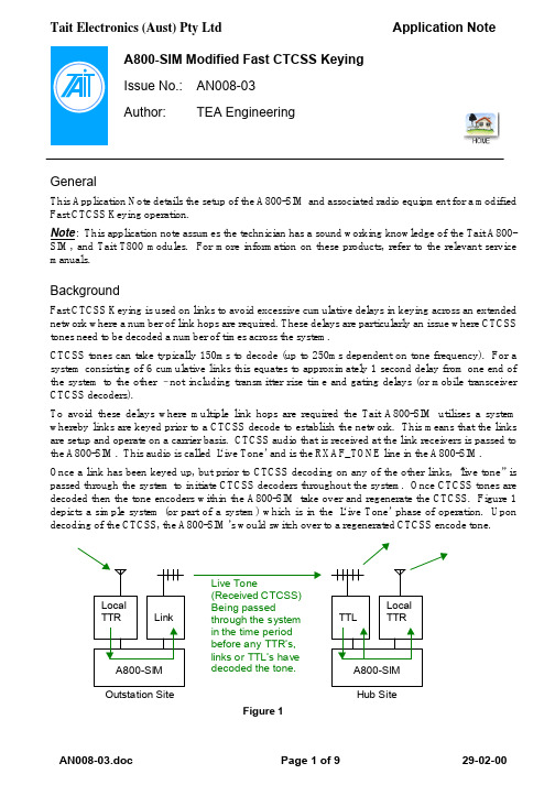
A800-SIM Modified Fast CTCSS KeyingIssue No.:AN008-03Author:TEA EngineeringGeneralThis Application Note details the setup of the A800-SIM and associated radio equipment for a modified Fast CTCSS Keying operation.Note: This application note assumes the technician has a sound working knowledge of the Tait A800-SIM, and Tait T800 modules. For more information on these products, refer to the relevant service manuals.BackgroundFast CTCSS Keying is used on links to avoid excessive cumulative delays in keying across an extended network where a number of link hops are required. These delays are particularly an issue where CTCSS tones need to be decoded a number of times across the system.CTCSS tones can take typically 150ms to decode (up to 250ms dependent on tone frequency). For a system consisting of 6 cumulative links this equates to approximately 1 second delay from one end of the system to the other – not including transmitter rise time and gating delays (or mobile transceiver CTCSS decoders).To avoid these delays where multiple link hops are required the Tait A800-SIM utilises a system whereby links are keyed prior to a CTCSS decode to establish the network. This means that the links are setup and operate on a carrier basis. CTCSS audio that is received at the link receivers is passed to the A800-SIM. This audio is called ‘Live Tone’ and is the RXAF_TONE line in the A800-SIM.Once a link has been keyed up, but prior to CTCSS decoding on any of the other links, “live tone” is passed through the system to initiate CTCSS decoders throughout the system. Once CTCSS tones are decoded then the tone encoders within the A800-SIM take over and regenerate the CTCSS. Figure 1 depicts a simple system (or part of a system) which is in the ‘Live Tone’ phase of operation. Upondecoding of the CTCSS, the A800-SIM’s would switch over to a regenerated CTCSS encode tone.Figure 1Outstation Site Hub Site(Received CTCSS)Being passedthrough the systemin the time periodbefore any TTR’s,links or TTL’s havedecoded the tone.The advantage of a system setup like this is that all transmitters can key up within milliseconds of each other, almost regardless of the topography of the system. This is true for a system with up to as many as six or seven link hops. After this an additional CTCSS decode period can occur due to the degradation of the retransmitted ‘Live Tone’. This however does not normally cause any problems to speech access times or to mobile voting system.A disadvantage of a system setup like this is that a carrier being received by a link can key up the local repeaters, even without CTCSS tone. This would allow interference on links to key up the repeaters. PurposeThis Application Note details a setup which does not let local repeaters key up until links get a valid decode on their received CTCSS audio.The procedure used in this Application Note is only applicable for certain restricted system architectures as it effectively reduces the maximum number of ports available on the A800-SIM. This needs to be considered prior to implementation.The main idea with this setup is that separate carrier gate and decode gate paths are setup in the A800-SIM for the local TTR and the link or TTL(Talk Through Link). This enables carrier gates and decode gates to be routed individually. Carrier gates are then setup to be routed only to links and TTL’s, and decode gates are setup to be routed only to the local repeaters (TTR).With this configuration, local TTR receivers are configured the same as links and TTL’s. This means they are configured to pass (output) a carrier gate and a ‘Live Tone’ signal.Using this setup, all repeaters in the system will transmit at virtually the same time, as long as the same CTCSS decode tone is used on all repeaters and links. If not, bases at different sites will not transmit at the same time, because of extra CTCSS decodes required between the first TTR and any remote links decoding.Important - This application noteassumes the connection of a single TTR and one link (or TTL). The TTR is connected to port 1 on the A800-SIM. The link is connected to port 3 or if the link is a TTL, for instance at a hub site, then it is connected to Port 2.Ports 4, 5 and 6 are used for separate decode input signals parallel to Ports 1, 2 & 3 respectively, and should not be connected to external equipment. The A800-SIM ports 7 & 8 are still free and will be configured to operate as the voting pulse input ports on hub sites that require a voting pulse to be generated. Figure 2 shows the connection of a typical hub site with a single base and a TTL to a A800-SIM.Figure 2The other thing to consider when following this procedure is that of Hub Site generated vote pulses. Vote pulses generated from the A800-SIM at the Hub Site will have one CTCSS decode time period difference between the Hub Site TTR transmitting and any/all Outstation Site TTR’s transmitting. This is because at the Hub Site the vote pulse is generated locally, so the local TTR will be keyed up instantly, but at Outstation Sites the link must achieve a CTCSS decode before keying the local TTR. This is not a problem as the Tait T2020 mobile operating in the system can have their Vote Lead In Delay programmed accordingly to handle the delay. A programmed time period of 150ms to 200ms should be adequate.If other brands of mobile radios are being used in the system, and these radios voting system cannot deal with the delays that can happen in the system, a work around can be implemented. This work around is applied to the Hub Site A800-SIM to delay the key-up of the local TTR during a vote pulse. Basically it involves connecting an A800-SIB- VP Vote Pulse Generator (based on the A800-SIB board) to ports 7 and 8 of the Hub Site A800-SIM. Once connected, no other configuration is required inside the A800-SIM.The A800-SIB-VP Vote Pulse Generator gives 2 independent outputs to use as TX Key lines. One output keys up the link transmitters only (not the TTR) with CTCSS which gives the outstation sites time to receive and decode the voting pulse, and then approx. 150mS later (1x CTCSS decode period) applies a 2nd key to the local TTR to key the TTR transmitter up with CTCSS on the voting pulse. In doing this, the limited operation & functionality of these mobiles can be overcome. For more information, please refer to the A800-SIB-VP documentation.A800-SIB-VP ModulePartsThe parts required are as follows:Part Number Description Supplier Qty. Misc.Miscellaneous workshop consumables, e.g. solder,wire, etc.N/A1 Procedure1.All T800 Receivers and Transmitters need to be modified as per Section 3.2 Basic Mods, in theA800-SIM Service Manual(AM8-SIM). Section 3.3 Optional Mods/Settings of the A800-SIM Service Manual also should be applied as follows :3.3.1 – Series II Programming & 2nd D Range - Optional to all modules but recommended.3.3.2 – Transmitter Fast Keying – Apply to all transmitters/exciters(except if they are to go on solar sites)3.3.3 – Receiver Fast Gating – Apply to all link receivers (not to repeater receivers).3.3.4 – Fast CTCSS Keying - Apply to all receivers (repeaters and links).3.3.5 – Link Receiver Mute Crash - Apply to all link receivers (not to repeater receivers).3.3.6 – CTCSS Encode Tone for Local Transmitter – Optional.The extra modification needed for the repeater receivers are to bring out the carrier gate line and the live tone audio. These are the signals on the A800-SIM ports RX1 to RX8 pin 11 RXGATE and pin 7 RXAF-TONE. Any other brand of radio equipment being used with the A800-SIM must also be configured to provide these signals. For more information on this, contact your local Tait representative.2.Remove the A800-SIM top lid. Remove the A800-SIM3 PCB from its 2RU 19” rack enclosure.This is done by unplugging the 16 way ribbon cables from ports RX1 to RX8 and TX1 to TX8, and removing the figure 8 speaker cable from the two way PCB terminal block S2. Next remove the six M3 x 6mm Pan Pozi screws holding the PCB down.3.On the bottom of the A800-SIM PCB, place wire links from RX1 pin 12 to RX4 pin 12, RX2 pin12 to RX5 pin 12, RX3 pin 12 to RX6 pin 12. This routes the RXDEC signals from ports 1, 2 and3 to ports 4, 5 and 6 respectively.4.Refit the A800-SIM PCB to its 2RU 19”rack enclosure, in the reverse order as Step 2.5.On the A800-SIM PCB, ensure that the 16 pin IDC header cable that connects to the RX D Rangeon Port 7 is plugged into the 16 pin IDC pin strip marked TARA. Also ensure that the 16 pin IDC header cable that connects to the RX D Range on Port 8 is plugged into the 16 pin IDC pin stripmarked T802.6.On the A800-SIM PCB, solder links LK71 to LK78should be setup as per Table 1. This sets up ports 1,2 and3 for normal carrier operation, and sets ports4, 5 and 6 for decode operation (i.e. routes port 4, 5 and 6 pin 12 input RXDEC to the Gate Matrix [via relays RL19, RL23, and RL22]). The links LK77and LK78 are setup for decode operation so anyexternal A800-SIB-VP Vote Pulse Generator willkey up the A800-SIM with CTCSS Encode tonesenabled.Table 1.Link SettingLK711-2LK721-2LK731-2LK742-3LK752-3LK762-3LK772-3LK782-37. Configure the Audio matrix, Gate matrix, Receiver Primary Tone Inputs matrix, and the PTT Output (Tails) matrix as for either Hub or Outstation operation. Refer to the following sections Hub Site Setup or Outstation Site Setup.The sections Hub Site Setup and Outstation Site Setup are not a complete list of configuration requirement for the A800-SIM, but simply detail the particular link setting that are important for the Modified Fast Keying type of operation. Each A800-SIM will still need other configurations,dependant on the type of system being setup. For more information, please refer to the A800-SIM service manual (AM8-SIM.pdf).8. For Outstation Sites, the Link on Port 3 will need to have RX Disable setup on it. Refer toSection 6.7 “RX Disable” in the A800-SIM Service Manual (AM8-SIM.pdf) for more information on receive disable. Note that KL Bases setup as End Site Links need their receive disable setup internally. Even though KL Bases have their receive disable setup internally, it is recommended that the A800-SIM port connected to the End Site Link be configured as per the A800-SIMService Manual. The reason for this is for compatibility and flexibility. For more information on KL Bases used with A800-SIM’s, refer to the Application Note AN002.9. Refer to Section 5.5 Setup of the A800-SIM service manual (AM8-SIM.pdf) for information on setting up the A800-SIM levels, etc.10. In addition to the TX Tail and Soft Off tail setup for a hub site, the Soft Off tail needs to be setup at all outstations as well. This is because the soft off from the hub does not get through from the link to the local repeater, because the link is tone guarded before the link will key the local repeater. The duration of all Soft Off tails at all site should be adjusted to be of the same time period.11. On the rear of the A800-SIM, place labels to identify ports 1 to 3, as per Figure 3.A800-SIM 19” 2RU Rack Rear ViewReceiver Input PortsTransmitter Output PortsDC InFigure 3Place Labels HereHub Site SetupThe link settings detailed here assume a Hub Site configuration consisting of one TTR connected to port 1 and one TTL connected to port 2.Audio MatrixTransmitter OutputsReceiver TTR TTL Link N/C N/C N/C N/C N/CInputs12345678TTR – 1X X X X X X X XTTL – 2X X X X X X X XLink – 3X X-X X X X X 4X X X-X X X X5X X X X-X X X6X X X X X-X X7X X X X X X-X8X X X X X X X-TT_AF*X X X X X X X XX = Solder Link in place- = No Solder LinkThe links that are important are highlighted in the table above. The setup of this matrix is the same as the default Hub Site shown in the A800-SIM service manual.Gate MatrixReceiver Gate InputsPTT TTR Gate TTL Gate Link Gate TTR Dec TTL Dec Link Dec VP-I VP-D Outputs12345678TTR - 1---X X X-XTTL - 2X X X X X X X XLink - 3X X-X X-X X 4X X X-X X X X5X X X X-X X X6X X X X X-X X7X X X X X X-X8X X X X X X X-VP-I = Instant Voting Pulse Input VP-D = Delayed Voting Pulse InputX = Solder Link in place- = No Solder LinkThe links that are important are highlighted in the table above. With the links setup as shown in this matrix, you can see that RX GATE signals from the local TTR are set to go directly to the TTL, but RX DEC from the local TTR will go to both the TTR and the TTL. The TTL RX GATE is set to go to the TTL, but RX DEC from the TTL will go to both the TTR and the TTL. This means that RX GATE signals from anywhere will be routed to the TTL, but only an RX DEC from the TTR or TTL will key up the local TTR.Hub Site Setup Cont.Receiver Primary Tone Inputs12345678Tail X X X X X X--No Tail------X XX = Solder Link in place- = No Solder LinkThe links that are important are highlighted in the table above. The setup of this matrix is almost the same as the default Hub Site shown in the A800-SIM service manual.PTT Outputs (Tail)12345678Tail X X X X X X X XX = Solder Link in place- = No Solder LinkThe links that are important are highlighted in the table above. The setup of this matrix is the same as the default shown in the A800-SIM service manual.Outstation Site SetupThe link settings detailed here assume a Outstation Site configuration consisting of one TTR connected to port 1 and one Link connected to port 3.Audio MatrixTransmitter OutputsReceiver TTR TTL Link N/C N/C N/C N/C N/CInputs12345678TTR - 1X X X X X X X XTTL - 2X X X X X X X XLink - 3X X-X X X X X 4X X X-X X X X5X X X X-X X X6X X X X X-X X7X X X X X X-X8X X X X X X X-TT_AF*X X X X X X X XX = Solder Link in place- = No Solder LinkThe links that are important are highlighted in the table above. The setup of this matrix is the same as the default Hub Site shown in the A800-SIM service manual. In this configuration, the default Hub Site setup is also suitable for the Outstation Sites as well.Gate MatrixReceiver Gate InputsPTT TTR Gate TTL Gate Link Gate TTR Dec TTL Dec Link DecOutputs12345678TTR – 1---X X X-XTTL – 2X X X X X X X XLink – 3X X-X X-X X 4X X X-X X X X5X X X X-X X X6X X X X X-X X7X X X X X X-X8X X X X X X X-X = Solder Link in place- = No Solder LinkThe links that are important are highlighted in the table above. With the links setup as shown in this matrix, you can see that RX GATE signals from the local TTR are set to go directly to Link, but RX DEC from the local TTR will go to both the TTR and the Link. The Link RX GATE is set to go nowhere, and RX DEC from the Link will go to the TTR. This means that RX GATE signals from the TTR will be routed to the Link, but only an RX DEC from the TTR or the Link will key up the local TTR.Outstation Site Setup Cont.Receiver Primary Tone Inputs12345678Tail--------No Tail X X X X X X X XX = Solder Link in place- = No Solder LinkThe links that are important are highlighted in the table above. The setup of this matrix is the same as the default Outstation Site described in the A800-SIM service manual.PTT Outputs (Tail)12345678Tail X X-X X X X XX = Solder Link in place- = No Solder LinkThe links that are important are highlighted in the table above. The setup of this matrix is similar to the Hub Site setup, except for link 3. Link 3 is not fitted because we don’t want the locally generated Soft Off tails to be sent back down the link.The PTT Output (Tail) links are normally only used at the hub to output the system tails out to all of the system. It also needs to be setup at all of the other sites so the local repeater can output the soft off tails, hence the link on 1. Link are left on 2, & 4 to 8 for compatibility with the Hub Site configuration.。
Panduit Cable Ties 产品选择指南说明书

Cable TiesProduct Selection Guide Panduit offers a broad selection of industry approved styles, sizes, and materials to meet a full range of electrical, industrial, and networking applications.Cable Tie Industry ApprovalsPLT Pan-Ty®Cable TiesMost comprehensive product offeringSG Super-Grip® Cable TiesWithstand rough installationsBT Dome-Top® Barb Ty Cable TiesMetal locking barb; infinite adjustabilityPLWS P an-Ty® Wide Strap Cable TiesIdeal for Heavy Duty applicationsDT Dura-Ty® Cable TiesAcetal material; 20+ years outdoor service lifeCBR C ontour-Ty® Cable TiesLow profile head, parallel-entry, outside teethHV Hyper-V™ Cable TiesTeeth on both sides; 2-wedge locking designSST Sta-Strap® Cable TiesTwo-piece design, low thread force, lightweightERT Elastomeric Cable TiesFlexible, elastic material, UL 94V-0, releasablePLDC P an-Ty® Double Clamp Cable TiesIdeal for Heavy Duty application2PLT SG BT DT CBR HV SST ERT PLWS PLDC Comprehensive Cable Tie SolutionsFor more detailed information, visit the Panduit website at /cabletiesCross Sections: SM = Subminiature, M = Miniature, I = Intermediate, S = Standard, HS = Heavy-Standard, LH = Light-Heavy, H = Heavy, EH = Extra-HeavyCheck mark indicates material availability in that product family for all cross sections.n TEFZEL is a registered trademark of The Chemours Company.sHALAR is a registered trademark of Ausimont USA, Inc.* T efzel material contains Flourine, but in accordance to IEC61249-2-21, which calls out Chlorine and Bromine, but not Flourine, meets the definition of Halogen-Free.Note 1: Check UL file for specific part number rating Note 2: B ased upon UL RTI for electrical properties; mechanicalwithout impact carries a 240° C (464° F) RTI rating34Material Selection Criteria© 2020 Panduit Corp.ALL RIGHTS RESERVEDPrinted in the U.S.A.CTSG05-SA-ENGReplaces CTSG04--SA-ENG4/2020Complete Your Bundling SystemManual Cable Tie Installation ToolsnDesigned to speed installation for lower installed cost n Flush tie cut-off limits exposure to sharp edgesn A full line of lightweight, ergonomic hand tools available n Panduit leads the industry in reliability and performanceAutomatic Cable Tie Installation Systemsn An efficient solution for high volume harnessing, assembly, fasteningand packaging applicationsn High speed tools lower installed cost and reduce operator fatigue n Wrap, tension, and cut off cable ties in less than one second n Microprocessor based controller monitors system performance for production data and reportingCustom Imprinting Servicen Products available for custom imprinting include cable ties, marker plates,marker and flag ties, hook and loop wrap tiesn Results in a professional, high quality appearance for identification and labeling as well as promotional purposesn Options include company logos, website addresses, sequential numbering, phone numbers, graphics and textCable AccessoriesnComprehensive line of mounts, clips, and clamps that organizes and routes cables, speeds and simplifies installations, and lowers overall installed cost Installation methods include adhesive backed, user applied adhesive, screws, rivets and push barbn Accessories provide long term reliability while cable clips and clamps offer a one-piece solution to save time and reduce inventoryStainless Steel Cable Tiesn Durable method of bundling, fastening and permanent identificationin applications where severe environmental conditions existn Engineered for safety, productivity and durability by providing round edgesand smooth surfaces, easy threading, high loop tensile strength and tight clampingToolsServicesRelated ProductsCable Tie Installation ToolsPanduit offers the most preferred hand-operated tools in the industry. These versatile tools can be used for production, maintenance or construction applications. Panduit cable tie installation tools promote worker safety, help reduce downtime, improve productivity and provide the lowest total installed cost. As with allPanduit products, quality in design and production along with customer service excellence, are assured.GTS-En Used with SM, M, I, and S cable tiesn Ergonomic design lowers the risk of repetitivemotion injuries. Lowest activation and impactforce to installer’s handGS2B-En Used with SM, M, I, and S cable ties n Metal tool with a durable powder coat finish n Ergonomic design lowers the risk of repetitivemotion injuries. Lowest activation and impactforce to installer’s handGTH-En Used with S, HS, LH, and H cable ties n Ergonomic design lowers the risk of repetitivemotion injuries. Lowest activation and impact force to installer’s handGS4H-En Used with S, HS, LH, and H cable ties n Metal tool with a durable powder coat finish n Ergonomic design lowers the risk of repetitivemotion injuries. Lowest activation and impactforce to installer’s hand GS4EH-En Used with LH, H, and EH cable ties n Metal tool with a durable powder coat finish n Ergonomic design lowers the risk of repetitivemotion injuries. Lowest activation and impactforce to installer’s handPTSn Used with SM, M, I, and S cable ties n Ergonomic design with impact resistant resinhousing and black knob; replacement parts canbe part of a scheduled maintenance program PTHn Used with S, HS, LH, and H cable ties n Ergonomic design with impact resistant resinhousing and red knob; replacement parts canbe part of a scheduled maintenance programPneumatic Tool Accessoriesn Visit for our complete lineof pneumatic tool accessoriesContactCustomerServicebyemail:**************or by phone: 800-777-3300Visit us at /cabletiesFor more informationCable Tie ToolsPneumatic Hand Tools5。