1031036C中文资料
STPCC0366BTC3资料

®STPC CONSUMER-SPC Compatible Embeded MicroprocessorADVANCED DATA1/5129/10/99Figure 1.Logic Diagrams POWERFUL x86PROCESSORs 64-BIT 66MHz SDRAM UMA CONTROLLER s VGA &SVGA CRT CONTROLLER s 2D GRAPHICS ENGINE s VIDEO INPUT PORTsVIDEO PIPELINE -UP-SCALER-VIDEO COLOR SP ACE CONVERTER -CHROMA &COLOUR KEY SUPPORT sTV OUTPUT-3-LINE FLICKER FILTER-CCIR 601/656SCAN CONVERTER-NTSC /PAL COMPOSITE,RGB,S-VIDEO s PCI MASTER /SLAVE CONTROLLER s ISA MASTER /SLAVE CONTROLLER sINTEGRA TED PERIPHERAL CONTROLLER -DMA CONTROLLER-INTERRUPT CONTROLLER -TIMER /COUNTERSs OPTIONAL 16-BIT LOCAL BUS INTERFACE s EIDE CONTROLLER s I C INTERFACEs POWER MANAGEMENT UNIT s3.3V OPERA TIONSTPC CONSUMER-S OVERVIEWThe STPC Consumer-S integrates a standard 5th generation x86core,a Synchronous DRAM con-troller,a graphics subsystem,a video input port,video pipeline,and support logic including PCI,ISA,and IDE controllers to provide a single con-sumer orientated PC compatible subsystem on a single device.The device is based on a tightly coupled Unified Memory Architecture (UMA),sharing the same memory array between the CPU main memory and the graphics and video frame buffers.The STPC Consumer-S is packaged in a 388Plastic Ball Grid Array (PBGA).PBGA388x86CoreHost I/F SDRAM CTRLSVGA GE VIPPCI m/sLB CTR PCI BusISA m/s IPCPCI m/s ISA Bus CRTCCursorMonitorTVIDE I/FPMUW.dogVideo PipelineC Key K Key LUTLocal BusEncoderTVOSTPC CONSUMER-S2/51s X86Processor cores Fully static 32-bit 5-stage pipeline,x86processor fully PC compatible.s Can access up to 4GB of external memory.s 8Kbyte unified instruction and data cache with write back and write through capability .s Parallel processing integral floating point unit,with automatic power down.s Fully static design for dynamic clock control.s Low power and system management modes.s SDRAM Controller s 64-bit data bus.s Up to 66MHz SDRAM clock speed.s Integrated system memory,graphic frame memory and video frame memory.s Supports 2MB up to 128MB memory.s Supports 8MB,16M,and 32MB DIMMs.s Supports buffered,non buffered,and registered DIMMss 4-line write buffers for CPU to DRAM and PCI to DRAM cycles.s 4-line read prefetch buffers for PCI masters.s Programmable latencys Programmable timing for DRAM parameters.s Supports -8,-10,-12,-13,-15memory parts s Supports 1MB up to 8MB memory hole.s 32-bit accesses not supported.s Autoprecharge not supported.s Power down not supported.s FPM and EDO not supported.s Graphics Controllers 64-bit windows accelerator .s Compatibility to VGA &SVGA standards.s Hardware acceleration for text,bitblts,transparent blts and fills.s Up to 64x 64bit graphics hardware cursor.s Up to 4MB long linear frame buffer.s8-,16-,and 24-bit pixels.s CRT Controllers Integrated 135MHz triple RAMDAC allowing for 1024x 768x 75Hz display .s 8-,16-,24-bit pixels.s Interlaced or non-interlaced output.s Video Input ports Accepts video inputs in CCIR 601mode.s Optional 2:1decimators Stores captured video in off setting area of the onboard frame buffer.s Video pass through to the onchip PAL/NTSC encoder for full screen video images.sHSYNC and B/T generation or lock onto external video timing source.s Video Pipelines Two-tap interpolative horizontal filter.s Two-tap interpolative vertical filter.s Color space conversion.s Programmab le window size.sChroma and color keying for integrated video overlay .s TV Outputs Programmab le two tap filter with gamma correction or three tap flicker filter.s Progressive to interlaced scan converter.s NTSC-M,PAL-M,P AL-B,D,G,H,I,PAL-N easy programmable video outputs.s CCIR601encoding with programmab le color subcarrier frequencies.s Line skip/insert capabilitys Interlaced or non-interlaced operation mode.s 625lines/50Hz or 525lines/60Hz 8bit multiplexed CB-Y -CR digital input.s CVBS and R,G,B simultaneous analog outputs through 10-bit DACs.s Cross color reduction by specific trap filtering on luma within CVBS flow.sPower down mode available on each DAC.STPC CONSUMER-S3/51s PCI Controllers Fully compliant with PCI 2.1specification.sIntegrated PCI arbitration interface.Up to 3masters can connect directly.External P AL allows for greater than 3masters.s Translation of PCI cycles to ISA bus.s Translation of ISA master initiated cycle to PCI.s Support for burst read/write from PCI master.sPCI clock is 1/3or 1/2Host clock.s ISA master/slave controllers Generates the ISA clock from either 14.318MHz oscillator clock or PCI clock s Supports programmable extra wait state for ISA cycless Supports I/O recovery time for back to back I/O cycles.s Fast Gate A20and Fast reset.s Supports the single ROM that C,D,or E.blocks shares with F block BIOS ROM.s Supports flash ROM.s Supports ISA hidden refresh.sBuffered DMA &ISA master cycles to reduce bandwidth utilization of the PCI and Host bus.NSP compliant.s Integrated Peripheral Controllers 2X8237/A T compatible 7-channel DMA controller.s 2X8259/A T compatible interrupt Controller.16interrupt inputs -ISA and PCI.s Three 8254compatible Timer/Counters.s Co-processor error support logic.s Supports external RTC.s Local Bus interfaces Multiplxed with ISA interface.s Low latency bus s 22-bit address bus.s 16-bit data bus with word steering capability .s Programmable timing (Host clock granularity)s 2Programmab le Flash Chip Select.s 5Programmab le I/O Chip Select.s Supports 32-bit Flash burst.s 2-level hardware key protection for Flash boot block protection.sSupports 2banks of 8MB flash devices with boot block shadowed to 0x000F0000.s IDE Interfaces Supports PIO and Bus Master IDE s Supports up to Mode 5Timings s Transfer Rates to 22MBytes/sec s Supports up to 4IDE devicess Concurrent channel operation (PIO &DMA modes)-4x 32-Bit Buffer FIFO per channel s Support for PIO mode 3&4.s Support for DMA mode 1&2.s Support for 11.1/16.6MB/s,I/O Channel Ready PIO data transfers.s Supports 13.3/16.6MB/s DMA data transfers s Bus Master with scatter/gather capability s Multi-word DMA support for fast IDE drives s Individual drive timing for all four IDE devices s Supports both legacy &native IDE modes s Supports hard drives larger than 528MB s Support for CD-ROM and tape peripherals s Backward compatibility with IDE (A TA-1).s Power Managements Four power saving modes:On,Doze,Standby ,Suspend.s Programmab le system activity detector s Supports SMM.s Supports STOPCLK.s Supports IO trap &restart.s Independent peripheral time-out timer to monitor hard disk,serial ¶llel ports.sSupports RTC,interrupts and DMAs wake-upGENERAL DESCRIPTION4/511GENERAL DESCRIPTIONAt the heart of the STPC Consumer-S is an ad-vanced 64-bit processor block,dubbed the 5ST86.The 5ST86includes a 486processor core along with a 64-bit SDRAM controller,advanced 64-bit accelerated graphics and video controller,a high speed PCI local-bus controller and Industry standard PC chip set functions (Interrupt control-ler,DMA Controller,Interval timer and ISA bus).The STPC Consumer-S makes use of a tightly coupled Unified Memory Architecture (UMA),where the same memory array is used for CPU main memory and graphics frame-buffer.This means a reduction in total system memory for sys-tem performances that are equal to that of a com-parable frame buffer and system memory based system,and generally much better,due to the higher memory bandwidth allowed by attaching the graphics engine directly to the 64-bit proces-sor host interface running at the speed of the proc-essor bus rather than the traditional PCI bus.The 64-bit wide memory array provides the sys-tem with 528MB/s peak bandwidth.This allows for higher resolution screens and greater color depth.The ‘standard’PC chipset functions (DMA,inter-rupt controller,timers,power management logic)are integrated together with the x86processor core;additional functions such as communica-tions ports are accessed by the STPC Consumer-S via internal ISA bus.The PCI bus is the main data communication link to the STPC Consumer-S chip.The STPC Con-sumer-S translates appropriate host bus I/O and Memory cycles onto the PCI bus.It also supports generation of Configuration cycles on the PCI bus.The STPC Consumer-S,as a PCI bus agent (host bridge class),fully complies with PCI specification 2.1.The chip-set also implements the PCI manda-tory header registers in Type 0PCI configuration space for easy porting of PCI aware system BI-OS.The device contains a PCI arbitration function for three external PCI devices.The STPC Consumer-S has two functionnal blocks sharing the same balls :The ISA /IPC /IDE block and the Local Bus /IDE block (see Ta-ble 3).Any board with the STPC Consumer-S should be built using only one of these two config-urations.At reset,the configuration is done by ‘strap op-tions’which initialises the STPC Consumer-S to the right settings.It is a set of pull-up or pull-down resistors on the memory data bus,checked on re-set,which auto-configure the STPC Consumer-S.GRAPHICS FUNCTIONSGraphics functions are controlled through the on-chip SVGA controller and the monitor display is produced through the 2D graphics display engine.This Graphics Engine is tuned to work with the host CPU to provide a balanced graphics system with a low silicon area cost.It performs limited graphics drawing operations which include hard-ware acceleration of text,bitblts,transparent blts and fills.The results of these operations change the contents of the on-screen or off-screen frame buffer areas of DRAM memory.The frame buffer can occupy a space up to 4Mbytes anywhere in the physical main memory and always starts from the bottom of the main physical memory.The graphics resolution supported is a maximum of 1280x1024in 65536colours and 1024x768in true color at 75Hz refresh rate and is VGA and SVGA compatible.Horizontal timing fields are VGA compatible while the vertical fields are ex-tended by one bit to accommodate above display resolution.VIDEO FUNCTIONSThe STPC Consumer-S provides several addition-al functions to handle MPEG or similar video streams.The Video Input Port accepts an encod-ed digital video stream in one of a number of in-dustry standard formats,decodes it,optionally decimates it,and deposits it into an off screen area of the frame buffer.An interrupt request can be generated when an entire field or frame has been captured.The video output pipeline incorpo-rates a video-scaler and color space converter function and provisions in the CRT controller to display a video window.While repainting the screen the CRT controller fetches both the video as well as the normal non-video frame buffer in two separate internal FIFOs.The video stream can be color-space converted (optionally)and smooth scaled.Smooth interpolative scaling in both horizontal and vertical direction are imple-mented.Color and Chroma key functions are also implemented to allow mixing video stream with non-video frame buffer.The video output passes directly to the RAMDAC for monitor output or through another optional color space converter (RGB to 4:2:2YCrCb)to the programmable anti-flicker filter.The flicker filter is configured as either a two line filter with gamma correction (primarily designed for DOS type text)or a 3line flicker filter (primarily designed for Win-dows type displays).The fliker filter is optional and can be software disabled for use with large screen area’s of video.GENERAL DESCRIPTION5/51The Video output pipeline of the STPC Consumer-S interfaces directly to the internal digital TV en-coder.It takes a 24bit RGB non-interlaced pixel stream and converts to a multiplexed 4:2:2YCrCb 8bit output stream,the logic includes a progres-sive to interlaced scan converter and logic to in-sert appropriate CCIR656timing reference codes into the output stream.It facilitates the high quality display of VGA or full screen video streams re-ceived via the Video input port to standard NTSC or PAL televisions.The digital PAL/NTSC encoder outputs interlaced or non-interlaced video in PAL-B,D,G,H,I PAL-N,PAL-M or NTSC-M standards and “NTSC-4.43”is also possible.The four frame (for PAL)or 2frame (for NTSC)burst sequences are internally generated,subcar-rier generation being performed numerically with CKREF as reference.Rise and fall times of syn-chronisation tips and burst envelope are internally controlled according to the relevant ITU-R and SMPTE recommendations.Video output signals are directed to four analog output pins through internal D/A converters giving,simultaneous R,G,B and composite CVBS out-puts.IDE INTERFACEAn industry standard EIDE (ATA 2)controller is built into the STPC Consumer-S.The IDE port is capable of supporting a total of four devices.POWER MANAGEMENTThe STPC Consumer-S core is compliant with the Advanced Power Management (APM)specifica-tion to provide a standard method by which the BIOS can control the power used by personal computers.The Power Management Unit module (PMU)controls the power consumption providing a comprehensive set of features that control the power usage and supports compliance with the United States Environmental Protection Agency’s Energy Star Computer Program.The PMU pro-vides following hardware structures to assist the software in managing the power consumption by the system.-System Activity Detection.-Three power down timers.-Doze timer for detecting lack of system activity for short durations.-Stand-by timer for detecting lack of system activ-ity for medium durations-Suspend timer for detecting lack of system activ-ity for long durations.-House-keeping activity detection.-House-keeping timer to cope with short bursts of house-keeping activity while dozing or in stand-by state.-Peripheral activity detection.-Peripheral timer for detecting lack of peripheral activity-SUSP#modulation to adjust the system perform-ance in various power down states of the system including full power on state.-Power control outputs to disable power from dif-ferent planes of the board.Lack of system activity for progressively longer period of times is detected by the three power down timers.These timers can generate SMI in-terrupts to CPU so that the SMM software can put the system in decreasing states of power con-sumption.Alternatively,system activity in a power down state can generate SMI interrupt to allow the software to bring the system back up to full power on state.The chip-set supports up to three power down states:Doze state,Stand-by state and Sus-pend mode.These correspond to decreasing lev-els of power savings.POWER DOWNPower down puts the STPC Consumer-S into sus-pend mode.The processor completes execution of the current instruction,any pending decoded in-structions and associated bus cycles.During the suspend mode,internal clocks are stopped.Re-moving power down,the processor resumes in-struction fetching and begins execution in the in-struction stream at the point it had stopped.Be-cause of the static nature of the core,no internal data is lost.GENERAL DESCRIPTION6/51Figure 2.Functionnal description.x86CoreHost I/F SDRAM I/FSVGA GE VIPPCI m/sLocal Bus I/FPCI BUSISA m/sIPC82C206PCI m/sISA BusCRTCHW CursorMonitorTV-Pixel formating -Scaler-Colour SpaceIDE I/FPMU watch-Video PipelineColour Key Chroma KeyLUTLocal BusNTSC/PAL EncoderTVO-CSC -FF -CCIRCC IR InputGENERAL DESCRIPTION7/51Figure 3.Typical ApplicationSTPC Consumer-SISAPCI4x 16-bit SDRAMsSuper I/O2x EIDEFlashKeyboard /Mouse Serial Ports Parallel Port FloppyMonitorTVVideoSVGACCIR601CCIR656S-VHS RGB PAL NTSCIRQDMA.REQDMA.ACKDMUXDMUXMUXMUXRTCGENERAL DESCRIPTION 8/51Update History for Video controller chapter9/511.1UPDATE HISTORY FOR VIDEO CONTROLLER CHAPTERThe following changes have been made to the General Description Chapter on 29/10/99.Section Change Text1Removed“The STPC Consumer-S has in addition to the 5ST86a TFT output,a Local Bus interface,a WatchDog and a JTAG interface.”PIN DESCRIPTION10/512PIN DESCRIPTION2.1INTRODUCTIONThe STPC Consumer-S integrates most of the functionalities of the PC architecture.As a result,many of the traditional interconnections between the host PC microprocessor and the peripheral devices are totally internal to the STPC Consum-er-S.This offers improved performance due to the tight coupling of the processor core and these pe-ripherals.As a result many of the external pin con-nections are made directly to the on-chip peripher-al functions.Figure 2.1shows the STPC Consumer-S external interfaces.It defines the main busses and their function.Table 2.1describes the physical imple-mentation listing signals type and their functionali-ty.Table 2.2provides a full pin listing and descrip-tion of pins.Table 2.5provides a full listing of pin locations of the STPC Consumer-S package by physical connection.Note:Several interface pins are multiplexed with other functions,refer to Table 2.3and Table 2.4for further detailsTable 2.1.Signal DescriptionGroup nameQtySystem Clocks &Resets 11Memory Interface 95PCI interface 60ISA 7989IDE34Local Bus 49Video Input 11TV Output8VGA Monitor interface 8Grounds 71V DD29Analog specific V CC /V DD 6Total Pin Count388Figure 2.1.STPC Consumer-S External InterfacesPCIx86SDRAM VGAVIPTVSYSISA/IDE/LB958118601189STPC CONSUMER-STable2.2.Definition of Signal PinsSignal Name Dir Description Qty BASIC CLOCKS AND RESETSSYSRSTI#I System Power Good Input1 SYSRSTO#O System Reset Output1 XTALI I14.3MHz Crystal Input1 XTALO I/O14.3MHz Crystal Output-External Oscillator Input1 HCLK I/O Host Clock(Test)1 DEV_CLK O24MHz Peripheral Clock(floppy drive)1 DCLK I/O27-135MHz Graphics Dot Clock1MEMORY INTERFACEMCLKI I Memory Clock Input1 MCLKO O Memory Clock Output1CS#[3:0]O DIMM Chip Select4MA[11:0]O Memory Row&Column Address12MD[63:0]I/O Memory Data64 RAS#[1:0]O Row Address Strobe2 CAS#[1:0]O Column Address Strobe2 MWE#O Write Enable1 DQM[7:0]O Data Input/Output Mask8PCI INTERFACEPCI_CLKI I33MHz PCI Input Clock1PCI_CLKO O33MHz PCI Output Clock(from internal PLL)1AD[31:0]I/O PCI Address/Data32 CBE#[3:0]I/O Bus Commands/Byte Enables4 FRAME#I/O Cycle Frame1 IRDY#I/O Initiator Ready1 TRDY#I/O Target Ready1 LOCK#I PCI Lock1 DEVSEL#I/O Device Select1 STOP#I/O Stop Transaction1 PAR I/O Parity Signal Transactions1 SERR#O System Error1 PCIREQ#[2:0]I PCI Request3PCI_GNT#[2:0]O PCI Grant3PCI_INT[3:0]I PCI Interrupt Request4 VDD5I5V Power Supply for PCI ESD protection4ISA CONTROLISA_CLK O ISA Clock Output-Multiplexer Select Line For IPC1ISA_CLK2X O ISA Clock x2Output-Multiplexer Select Line For IPC1 OSC14M O ISA bus synchronisation clock1LA[23:17]O Unlatched Address7SA[19:0]I/O Latched Address20SD[15:0]I/O Data Bus16 ALE O Address Latch Enable1 MEMR#,MEMW#I/O Memory Read and Memory Write2 SMEMR#,SMEMW#O System Memory Read and Memory Write211/51Table2.2.Definition of Signal PinsSignal Name Dir Description Qty IOR#,IOW#I/O I/O Read and Write2 MCS16#,IOCS16#I Memory/IO Chip Select162 BHE#O System Bus High Enable1 ZWS#I Zero Wait State1 REF#O Refresh Cycle.1 MASTER#I Add On Card Owns Bus1 AEN O Address Enable1 IOCHCK#I I/O Channel Check.1 IOCHRDY I/O I/O Channel Ready(ISA)-Busy/Ready(IDE)1 ISAOE#O ISA/IDE Selection1 GPIOCS#I/O General Purpose Chip Select1 IRQ_MUX[3:0]I Time-Multiplexed Interrupt Request4 DREQ_MUX[1:0]I Time-Multiplexed DMA Request2 DACK_ENC[2:0]O Encoded DMA Acknowledge3 TC O ISA Terminal Count1 RTCAS O Real Time Clock Address Strobe1 RMRTCCS#I/O ROM/RTC Chip Select1 KBCS#I/O Keyboard Chip Select1 RTCRW#I/O RTC Read/Write1 RTCDS I/O RTC Data Strobe1LOCAL BUSPA[21:0]O Address Bus22 PD[15:0]I/O Data Bus16 PRD1#,PRD0#O Peripheral Read Control2 PWR1#,PWR0#O Peripheral Write Control2 PRDY#I Data Ready1 FCS1#,FCS0#O Flash Chip Select2 IOCS#[3:0]O I/O Chip Select4IDE CONTROLDA[2:0]O Address Bus3 DD[15:0]I/O Data Bus16 PCS3#,PCS1#,SCS3#,SCS1#O Primary&Secondary Chip Selects4 DIORDY O Data I/O Ready1 PIRQ,SIRQ I Primary&Secondary Interrupt Request2 PDRQ,SDRQ I Primary&Secondary DMA Request2 PDACK#,SDACK#O Primary&Secondary DMA Acknowledge2 PDIOR#,SDIOR#O Primary&Secondary I/O Channel Read2 PDIOW#,SDIOW#O Primary&Secondary I/O Channel Write2MONITOR INTERFACERED,GREEN,BLUE O Analog Red,Green,Blue3 VSYNC O Vertical Sync1 HSYNC O Horizontal Sync1 VREF_DAC I DAC Voltage reference1 RSET I Resistor Set1 COMP I Compensation112/5113/512.2SIGNAL DESCRIPTIONS 2.2.1BASIC CLOCKS AND RESETSSYSRSTI#System Reset/Power good.This input is low when the reset switch is depressed.Other-wise,it reflects the power supply’s power good signal.This input is asynchronous to all clocks,and acts as a negative active reset.The reset cir-cuit initiates a hard reset on the rising edge of this signal.SYSRSTO#Reset Output to System.This is the system reset signal and is used to reset the rest of the components (not on Host bus)in the system.The ISA bus reset is an externally inverted buff-ered version of this output and the PCI bus reset is an externally buffered version of this output.XTALI 14.3MHz Crystal InputXTALO 14.3MHz Crystal Output.These pins are connected to the 14.318MHz crystal to provide the reference clock for the internal frequency syn-thesizer to generate all the other clocks.A 14.318MHz Series Cut Crystal should be con-nected between these two pins.Balance capaci-tors of 15pF should also be added.In the event of an external quarzt oscillator providing the masterclock signal to the STPC Consumer-S device,the TTL signal should be provided on XTALO.HCLK Host Clock.This clock supplies the CPU and the host related blocks.This clock can e dou-bled inside the CPU and is intended to operate in the range of 25to 100MHz.This clock in generat-ed internally from a PLL but can be driven directly from the external system.DCLK Dot Clock /Pixel clock.This clock supplies the display controller,the video pipeline,the ram-dac,and the TV output logic.Its value is depend-ent on the selected display mode.Its frequency can be as high as 135MHz.This sig-nal is either driven by the internal PLL either by an external oscillator.The direction can be controlled by a strap option or an internal register bit.DEV_CLK 24MHz Peripheral Clock.This 24MHZ signal is provided as a convenience for the system integration of a Floppy Disk driver function in an external chip.VIDEO INPUT VCLK I 27-33MHz Video Input Port Clock1VIN I CCIR 601or 656YUV Video Data Input8VCSI/O Composite Synch or Horizontal line SYNC output 1ODD_EVENI/OFrame Synchronisation1ANALOG TV OUTPUTRED_TV,GREEN_TV,BLUE_TV O Analog RGB or S-VHS outputs 3CVBS O Analog video composite output1IREF1_TV I Reference current of 9bit DAC for CVBS 1VREF1_TV I Reference voltage of 9bit DAC for CVBS 1IREF2_TV I Reference current of 8bit DAC for R,G,B 1VREF2_TV I Reference voltage of 8bit DAC for R,G,B 1VSSA_TV I Analog Vss for DAC 1VDDA_TV I Analog Vdd for DAC 1MISCELLANEOUS SPKRD O Speaker Device Output1SCL I/O I C Interface -Clock /Can be used for VGA DDC[1]signal 1SDAI/O I C Interface -Data /Can be used for VGA DDC[0]signal 1SCAN_ENABLEI Reserved (Test pin)1Table 2.2.Definition of Signal PinsSignal NameDir DescriptionQty2.2.2MEMORY INTERFACEMCLKO Memory Clock Output.This clock is driv-ing the DIMMs on board and is generated from an internal PLL.The default value is66MHz.MCLKI Memory Clock Input.This clock is driving the SDRAM controller,the graphics engine and display controller.This input should be a buffered version of the MCLKO signal with the track lengths between the buffer and the pin matched with the track lengths between the buffer and the DIMMs.CS#[3:0]Chip Select These signals are used to disable or enable device operation by masking or enabling all SDRAM inputs except MCLK,CKE, and DQM.MA[11:0]Memory Address.Multiplexed row and column address lines.MD[63:0]Memory Data.This is the64-bit memory data bus.MD[40-0]are read by the device strap option registers during rising edge of SYSRSTI#.RAS#[1:0]Row Address Strobe.These signals enable row access and precharge.Row address is latched on rising edge of MCLK when RAS#is low.CAS#[1:0]Column Address Strobe.These sig-nals enable column access.Column address is latched on rising edge of MCLK when CAS#is low.MWE#Write Enable.Write enable specifies whether the memory access is a read(MWE#=H) or a write(MWE#=L).DQM#[7:0]Data Mask.Makes data output Hi-Z after the clock and masks the SDRAM outputs. Blocks SDRAM data input when DQM active.2.2.3PCI INTERFACEPCI_CLKI33MHz PCI Input Clock.This signal is the PCI bus clock input and should be driven from the PCI_CLKO pin.PCI_CLKO33MHz PCI Output Clock.This is the master PCI bus clock output.AD[31:0]PCI Address/Data.This is the32-bit multiplexed address and data bus of the PCI.This bus is driven by the master during the address phase and data phase of write transactions.It is driven by the target during data phase of read transactions.CBE#[3:0]Bus Commands/Byte Enables.These are the multiplexed command and byte enable signals of the PCI bus.During the address phase they define the command and during the data phase they carry the byte enable information. These pins are inputs when a PCI master other than the STPC Consumer-S owns the bus and outputs when the STPC Consumer-S owns the bus.FRAME#Cycle Frame.This is the frame signal of the PCI bus.It is an input when a PCI master owns the bus and is an output when STPC Consumer-S owns the PCI bus.IRDY#Initiator Ready.This is the initiator ready signal of the PCI bus.It is used as an output when the STPC Consumer-S initiates a bus cycle on the PCI bus.It is used as an input during the PCI cy-cles targeted to the STPC Consumer-S to deter-mine when the current PCI master is ready to complete the current transaction.TRDY#Target Ready.This is the target ready sig-nal of the PCI bus.It is driven as an output when the STPC Consumer-S is the target of the current bus transaction.It is used as an input when STPC Consumer-S initiates a cycle on the PCI bus.LOCK#PCI Lock.This is the lock signal of the PCI bus and is used to implement the exclusive bus operations when acting as a PCI target agent.14/51DEVSEL#I/O Device Select.This signal is used as an input when the STPC Consumer-S initiates a bus cycle on the PCI bus to determine if a PCI slave device has decoded itself to be the target of the current transaction.It is asserted as an output either when the STPC Consumer-S is the target of the current PCI transaction or when no other de-vice asserts DEVSEL#prior to the subtractive de-code phase of the current PCI transaction.STOP#Stop Transaction.Stop is used to imple-ment the disconnect,retry and abort protocol of the PCI bus.It is used as an input for the bus cy-cles initiated by the STPC Consumer-S and is used as an output when a PCI master cycle is tar-geted to the STPC Consumer-S.PAR Parity Signal Transactions.This is the parity signal of the PCI bus.This signal is used to guar-antee even parity across AD[31:0],CBE#[3:0], and PAR.This signal is driven by the master dur-ing the address phase and data phase of write transactions.It is driven by the target during data phase of read transactions.(Its assertion is identi-cal to that of the AD bus delayed by one PCI clock cycle)SERR#System Error.This is the system error sig-nal of the PCI bus.It may,if enabled,be asserted for one PCI clock cycle if target aborts a STPC Consumer-S initiated PCI transaction.Its asser-tion by either the STPC Consumer-S or by another PCI bus agent will trigger the assertion of NMI to the host CPU.This is an open drain output.PCIREQ#[2:0]PCI Request.This pin are the three external PCI master request pins.They indi-cates to the PCI arbiter that the external agents desire use of the bus.PCI_GNT#[2:0]PCI Grant.These pins indicate that the PCI bus has been granted to the master requesting it on its PCIREQ#.PCI_INT[3:0]PCI Interrupt Request.These are the PCI bus interrupt signals.VDD55V Power Supply.These power pins are necessary for5V ESD protection.In case the PCI bus is used in3.3V only,these pins can be con-nected to3.3V.2.2.4ISA INTERFACEISA_CLK,ISA_CLKX2ISA Clock x1,x2.These pins generate the Clock signal for the ISA bus and a Doubled Clock signal.They are also used as the multiplexor control lines for the Interrupt Controller Interrupt input lines.ISA_CLK is generated from either PCICLK/4or OSC14M/2.OSC14M ISA bus synchronisation clock Output. This is the buffered14.318Mhz clock for the ISA bus.LA[23:17]Unlatched Address.When the ISA bus is active,these pins are ISA Bus unlatched ad-dress for16-bit devices.When ISA bus is ac-cessed by any cycle initiated from PCI bus,these pins are in output mode.When an ISA bus master owns the bus,these pins are in input mode.SA[19:0]ISA Address Bus.System address bus of ISA on8-bit slot.These pins are used as an in-put when an ISA bus master owns the bus and are outputs at all other times.SD[15:0]I/O Data Bus.These pins are the exter-nal databus to the ISA bus.ALE Address Latch Enable.This is the address latch enable output of the ISA bus and is asserted by the STPC Consumer-S to indicate that LA23-17,SA19-0,AEN and SBHE#signals are valid. The ALE is driven high during refresh,DMA mas-ter or an ISA master cycles by the STPC Consum-er-S.ALE is driven low after reset.MEMR#Memory Read.This is the memory read command signal of the ISA bus.It is used as an in-put when an ISA master owns the bus and is an output at all other times.The MEMR#signal is active during refresh.MEMW#Memory Write.This is the memory write command signal of the ISA bus.It is used as an in-put when an ISA master owns the bus and is an output at all other times.SMEMR#System Memory Read.The STPC Con-sumer-S generates SMEMR#signal of the ISA bus only when the address is below one megabyte or the cycle is a refresh cycle.15/51。
100363中文资料
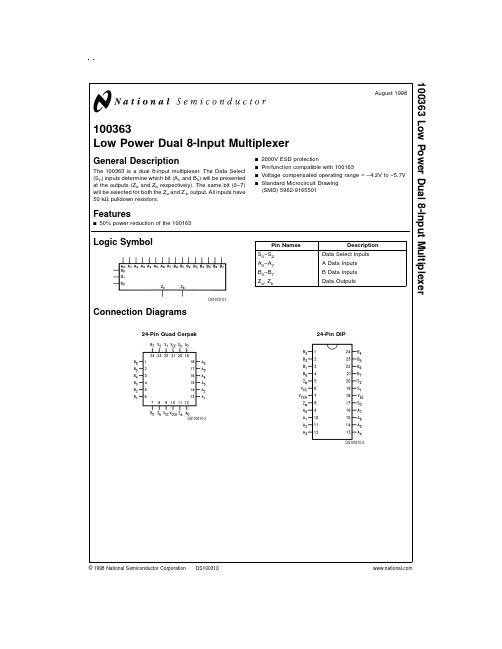
100363Low Power Dual 8-Input MultiplexerGeneral DescriptionThe 100363is a dual 8-input multiplexer.The Data Select (S n )inputs determine which bit (A n and B n )will be presented at the outputs (Z a and Z b respectively).The same bit (0–7)will be selected for both the Z a and Z b output.All inputs have 50k Ωpulldown resistors.Featuresn 50%power reduction of the 100163n 2000V ESD protectionn Pin/function compatible with 100163n Voltage compensated operating range =−4.2V to −5.7V nStandard Microcircuit Drawing (SMD)5962-9165501Logic SymbolPin Names DescriptionS 0–S 2Data Select Inputs A 0–A 7A Data Inputs B 0–B 7B Data Inputs Z a ,Z bData OutputsConnection DiagramsDS100310-124-Pin Quad CerpakDS100310-324-Pin DIPAugust 1998100363Low Power Dual 8-Input Multiplexer©1998National Semiconductor Corporation Logic DiagramDS100310-5 2Truth TableInputs OutputsSelect DataS2S1S0A7A6A5A4A3A2A1A0Z aB7B6B5B4B3B2B1B0Z bL L L L LL L L H HL L H L LL L H H HL H L L LL H L H HL H H L LL H H H HH L L L LH L L H HH L H L LH L H H HH H L L LH H L H HH H H L LH H H H HH=HIGH Voltage LevelL=LOW Voltage LevelBlank=X=Don’t Care3Absolute Maximum Ratings(Note1)If Military/Aerospace specified devices are required, please contact the National Semiconductor Sales Office/ Distributors for availability and specifications.Above which the useful life may be imparedStorage Temperature(T STG)−65˚C to+150˚C Maximum Junction Temperature(T J)Ceramic+175˚C V EE Pin Potential to Ground Pin−7.0V to+0.5V Input Voltage(DC)V EE to+0.5V Output Current(DC Output HIGH)−50mA ESD(Note2)≥2000V Recommended Operating ConditionsCase Temperature(T C)Military−55˚C to+125˚C Supply Voltage(V EE)−5.7V to−4.2V Note1:Absolute maximum ratings are those values beyond which the de-vice may be damaged or have its useful life impaired.Functional operation under these conditions is not implied.Note2:ESD testing conforms to MIL-STD-883,Method3015.Military VersionDC Electrical CharacteristicsV EE=−4.2V to−5.7V,V CC=V CCA=GND,T C=−55˚C to+125˚CSymbol Parameter Min Max Units T C Conditions NoteV OH Output HIGH Voltage−1025−870mV0˚C to+125˚C−1085−870mV−55˚C V IN=V IH(Max)Loading with(Notes3,4,5) V OL Output LOW Voltage−1830−1620mV0˚C to or V IL(Min)50Ωto−2.0V+125˚C−1830−1555mV−55˚CV OHC Output HIGH Voltage−1035mV0˚C to+125˚C−1085mV−55˚C V IN=V IH(Min)Loading with(Notes3,4,5) V OLC Output LOW Voltage−1610mV0˚C to or V IL(Max)50Ωto−2.0V+125˚C−1555mV−55˚CV IH Input HIGH Voltage−1165−870mV −55˚C to Guaranteed HIGH Signal for AllInputs(Notes3,4,5,6) +125˚CV IL Input LOW Voltage−1830−1475mV−55˚C to Guaranteed LOW Signal for All Inputs(Notes3,4,5,6)+125˚CI IL Input LOW Current0.50µA−55˚C to V EE=−4.2V(Notes3,4,5)+125˚C V IN=V IL(Min)I IH Input HIGH CurrentS n265µA0˚C toA n,B n340+125˚C V EE=−5.7V(Notes3,4,5)S n385µA−55˚C V IN=V IH(Max)A n,B n490I EE Power SupplyCurrent −87−30mA−55˚C to Inputs Open(Notes3,4,5)+125˚CNote3:F100K300Series cold temperature testing is performed by temperature soaking(to guarantee junction temperature equals−55˚C),then testing immediately without allowing for the junction temperature to stabilize due to heat dissipation after power-up.This provides“cold start”specs which can be considered a worst case condition at cold temperatures.Note4:Screen tested100%on each device at−55˚C,+25˚C,and+125˚C,Subgroups1,2,3,7,and8.Note5:Sample tested(Method5005,Table I)on each manufactured lot at−55˚C,+25˚C,and+125˚C,Subgroups A1,2,3,7,and8.Note6:Guaranteed by applying specified input condition and testing V OH/V OL.4AC Electrical Characteristics V EE=−4.2V to−5.7V,V CC=V CCA=GNDSymbol Parameter T C=−55˚C T C=+25˚C T C=+125˚CUnits Conditions Notes Min Max Min Max Min Maxt PLH Propagation Delay0.50 2.400.60 2.300.70 3.00nst PHL A0–A7,B0–B7to Output(Notes7,8,9)t PLH Propagation Delay0.80 3.000.90 2.800.80 3.40ns Figure1andt PHL S0–S2to Output Figure2t TLH Transition Time0.30 1.900.30 1.800.30 2.10ns(Note10)t THL20%to80%,80%to20%Note7:F100K300Series cold temperature testing is performed by temperature soaking(to guarantee junction temperature equals−55˚C),then testing immediately after power-up.This provides“cold start”specs which can be considered a worst case condition at cold temperatures.Note8:Screen tested100%on each device at+25˚C temperature only,Subgroup A9.Note9:Sample tested(Method5005,Table I)on each manufactured lot at+25˚C,Subgroup A9,and at+125˚C and−55˚C,temperatures,Subgroups A10and A11. Note10:Not tested at+25˚C,+125˚C,and−55˚C temperature(design characterization data).Test CircuitryDS100310-6Notes:V CC,V CCA=+2V,V EE=−2.5VL1and L2=equal length50Ωimpedance linesR T=50Ωterminator internal to scopeDecoupling0.1µF from GND to V CC and V EEAll unused outputs are loaded with50Ωto GNDC L=Fixture and stray capacitance≤3pFPin numbers shown are for flatpak;for DIP see logic symbolFIGURE1.AC Test Circuit5Switching WaveformsDS100310-7FIGURE2.Propagation Delay and Transition Times 6Physical Dimensions inches(millimeters)unless otherwise noted24-Pin Ceramic Dual-In-Line Package(D)NS Package Number J24E24-Pin Quad Cerpak(F)NS Package Number W24B7LIFE SUPPORT POLICYNATIONAL’S PRODUCTS ARE NOT AUTHORIZED FOR USE AS CRITICAL COMPONENTS IN LIFE SUPPORT DE-VICES OR SYSTEMS WITHOUT THE EXPRESS WRITTEN APPROVAL OF THE PRESIDENT OF NATIONAL SEMI-CONDUCTOR CORPORATION.As used herein:1.Life support devices or systems are devices or sys-tems which,(a)are intended for surgical implant intothe body,or (b)support or sustain life,and whose fail-ure to perform when properly used in accordancewith instructions for use provided in the labeling,can be reasonably expected to result in a significant injury to the user.2.A critical component in any component of a life support device or system whose failure to perform can be rea-sonably expected to cause the failure of the life support device or system,or to affect its safety or effectiveness.National Semiconductor Corporation AmericasTel:1-800-272-9959Fax:1-800-737-7018Email:support@National Semiconductor EuropeFax:+49(0)180-5308586Email:europe.support@Deutsch Tel:+49(0)180-5308585English Tel:+49(0)180-5327832Français Tel:+49(0)180-5329358Italiano Tel:+49(0)180-5341680National Semiconductor Asia Pacific Customer Response Group Tel:65-2544466Fax:65-2504466Email:sea.support@National Semiconductor Japan Ltd.Tel:81-3-5620-6175Fax:81-3-5620-6179100363L o w P o w e r D u a l 8-I n p u t M u l t i p l e x e rNational does not assume any responsibility for use of any circuitry described,no circuit patent licenses are implied and National reserves the right at any time without notice to change said circuitry and specifications.。
不锈钢牌号对照表

不锈钢牌号对照表
精选文档,供参考!
精选文档,供参考!
精选文档,供参考!
精选文档,供参考!
精选文档,供参考!
世界金属牌号对照表碳素结构钢
精选文档,供参考!
精选文档,供参考!
[返回]
优质碳素结构钢
精选文档,供参考!
精选文档,供参考!
精选文档,供参考!
精选文档,供参考!
精选文档,供参考!
精选文档,供参考!
[返回]
碳素工具钢
精选文档,供参考!
精选文档,供参考!
[返回]
合金结构钢
精选文档,供参考!
精选文档,供参考!
精选文档,供参考!
精选文档,供参考!
精选文档,供参考!
精选文档,供参考!
精选文档,供参考!
[返回]
淬透性合金结构钢
精选文档,供参考!
精选文档,供参考!
[返回]
精选文档,供参考!
弹簧钢
精选文档,供参考!
[返回]
滚动轴承钢
精选文档,供参考!
[返回]
高速工具钢
精选文档,供参考!
精选文档,供参考!
[返回]
不锈耐酸钢
精选文档,供参考!
精选文档,供参考!
精选文档,供参考!
精选文档,供参考!
[返回]
耐热钢
精选文档,供参考!
精选文档,供参考!
[返回]
精选文档,供参考!
易切结构钢
精选文档,供参考!
合金工具钢
精选文档,供参考!
精选文档,供参考!
精选文档,供参考!
(此文档部分内容来源于网络,如有侵权请告知删除,文档可自行编辑修改内容,供参考,感谢您的支持)
精选文档,供参考!。
SE1031中文资料
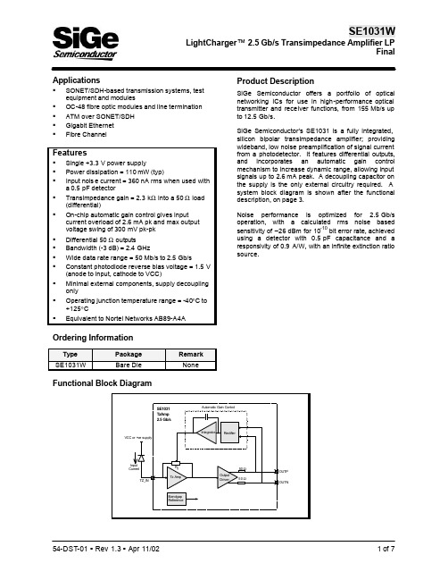
Applications§ SONET/SDH-based transmission systems, test equipment and modules§ OC-48 fibre optic modules and line termination § ATM over SONET/SDH§ Gigabit Ethernet§ Fibre ChannelFeatures§ Single +3.3 V power supply§ Power dissipation = 110 mW (typ)§ Input nois e current = 360 nA rms when used witha 0.5 pF detector§ Transimpedance gain = 2.3 kΩ into a 50 Ω load (differential)§ On-chip automatic gain control gives input current overload of 2.6 mA pk and max outputvoltage swing of 300 mV pk-pk§ Differential 50 Ω outputs§ Bandwidth (-3 dB) = 2.4 GHz§ Wide data rate range = 50 Mb/s to 2.5 Gb/s§ Constant photodiode reverse bias voltage = 1.5 V (anode to input, cathode to VCC)§ Minimal external components, supply decoupling only§ Operating junction temperature range = -40°C to +125°C§ Equivalent to Nortel Networks AB89-A4A Ordering InformationType Package Remark SE1031W Bare Die None Product DescriptionSiGe Semiconductor offers a portfolio of optical networking ICs for use in high-performance optical transmitter and receiver functions, from 155 Mb/s up to 12.5 Gb/s.SiGe Semiconductor’s SE1031 is a fully integrated, silicon bipolar transimpedance amplifier; providing wideband, low noise preamplification of signal current from a photodetector. It features differential outputs, and incorporates an automatic gain control mechanism to increase dynamic range, allowing input signals up to 2.6 mA peak. A decoupling capacitor on the supply is the only external circuitry required. A system block diagram is shown after the functional description, on page 3.Noise performance is optimized for 2.5 Gb/s operation, with a calculated rms noise based sensitivity of –26 dBm for 10-10 bit error rate, achieved using a detector with 0.5 pF capacitance and a responsivity of 0.9 A/W, with an infinite extinction ratio source.Functional Block DiagramBondpad DiagramBondpad DescriptionPad No. Name Description1 VCC Positive supply (+3.3 V), pads 1, 7 & 10 are connected on chip. Only one pad needsto be bonded.2 TZ_IN Input pad (connect to photodetector anode).3 VEE2 Negative supply (0V) – Note this is separate ground for the input stage, which is ACcoupled on chip. There is no DC current through this pad.4 VEE1 Negative supply (0V), pads 4,5 &6 are connected on chip. Only one pad needs to bebonded.5 VEE1 Negative supply (0V), pads 4, 5 &6 are connected on chip. Only one pad needs to bebonded.6 VEE1 Negative supply (0V), pads 4, 5 & 6 are connected on chip. Only one pad needs to bebonded.7 VCC Positive supply (+3.3 V), pads 1, 7 & 10 are connected on chip. Only one pad needsto be bonded.8 OUTN Negative differential voltage output.9 OUTP Positive differential voltage output.10 VCC Positive supply (+3.3 V), pads 1, 7 & 10 are connected on chip. Only one pad needsto be bonded.Functional DescriptionAmplifier front-endThe transimpedance front-end amplifies an input current from a photodetector, at pin TZ_IN, to produce a differential output voltage with the feedback resistor Rf determining the level of amplification (see the functional block diagram on page 1). An automatic gain control loop varies this resistor, to ensure that the output from the front-end does not saturate the output driver stage that follows. This gain control allows input signals of up to 2.6 mA peak.The input pin TZ_IN is biased at 1.5 V below the supply voltage VCC, allowing a photodetector to havea constant reverse bias by connecting the cathode to3.3 V. This enables full single rail operation.The front-end stage has its own supply ground connection (VEE2) to achieve optimum noise performance and maintain integrity of the high-speed signal path. The front-end shares the VCC (+3.3 V) connection with the remainder of the circuitry, which has a separate ground (VEE1).Output driver stageThe output driver acts as a buffer stage, capable of swinging up to 300 mVpk-pk differential into a 100 Ωload. The small output swings allow ease of use with low voltage post amplifiers (e.g. 3.3 V parts). Increasing optical input level gives a positive-going output signal on the OUTP pin.Automatic Gain Control (AGC)The AGC circuit monitors the voltages from the output driver and compares them to an internal reference level produced via the on-chip bandgap reference circuit. When this level is exceeded, the gain of the front-end is reduced by controlling the feedback resistor Rf.A long time-constant integrator is used within the control loop of the AGC with a typical low frequency cut-off of 10 kHz.System Block DiagramAbsolute Maximum RatingsThese are stress ratings only. Exposure to stresses beyond these maximum ratings may cause permanent damage to, or affect the reliability of t he device. Avoid operating the device outside the recommended operating conditions defined below.Symbol Parameter Min Max Unit VCC Supply Voltage –0.7 6.0 VV IO Voltage at any input or output –0.5 VCC+0.5 V–20 20 mAI IO Current sourced into any input or output exceptTZ_INI IO Current sourced into pin TZ_IN –5 5 mA–2 2 kVV ESD Electrostatic Discharge (100 pF, 1.5 kΩ) exceptTZ_IN–0.25 0.25 kVV ESD Electrostatic Discharge (100 pF, 1.5 kΩ) pinTZ_INTstg Storage Temperature –65 150 °C Recommended Operating ConditionsSymbol Parameter Min Typ Max Unit VCC Supply Voltage 3.1 3.3 3.5 VTj Operating Junction Temperature –40 125 °CDC Electrical CharacteristicsSymbol Parameter Min Typ Max UnitICC max Supply Current (max input current) 41 65 mAICC zero Supply Current (zero input current) 33 52 mAlagc AGC Threshold 42 µA pk-pk Vin Input Bias Voltage VCC–1.57 VCC–1.52 VCC–1.47 VVout Output Bias Voltage VCC–0.15 VRout Output Resistance 35 50 65 ΩAC Electrical CharacteristicsSymbol Parameter Min Typ Max Unit BW (3dB) Small Signal Bandwidth at –3dB point 1.8 2.4 GHz1.62.33.1 kΩTz Differential Transimpedance (50 Ω on each output,f = 100 MHz)Dri Input Data Rate 50 2500 Mb/s Voutmax Maximum Differential Output Voltage 300 mV pk-pk Flf Low Frequency Cut-off 10 20 kHzl OL Input Current before overload (2.5 Gb/s NRZ data) 2600 µA pk-pk Pol Optical Overload +1.6 dBm Nrms Input Noise Current (in 2 GHz) 360 500 nA rms Sens Optical Sensitivity [ calculated from input noise–26 dBm spectral density only, (10-10 BER) ]DC and AC electrical characteristics are specified under the following conditions:Supply Voltage (VCC).........................................3.1 V to 3.5 VJunction Temperature (Tj)..................................–40°C to 125°CLoad Resistor (R L)...............................................50 Ω AC coupled via 220 nF, for each outputPhotodetector Capacitance (Cd).......................0.5 pFInput bond wire inductance................................1 nHPhotodetector responsivity.................................0.9 A/WTransimpedance (Tz) measured with 4 µA mean photocurrentBondpad ConfigurationThe diagram below shows the bondpad configuration of the SE1031 Transimpedance Amplifier: Note that the diagram is not to scale. Bondpad openings are 82 µm x 82 µm. There are three VCC and three VEE1 pads for ease of wire bonding – the VCC and VEE1 pads respectively are connected on-chip and only one pad of each type is required to be bonded out.Applications InformationFor optimum performance it is recommended that the device be used in differential mode with the circuit shown in the diagram below.Note that all VCC pads (1, 7, 10) are connected on-chip, as are the VEE1 pads (4, 5, 6), and only one pad of each type is required to be bonded out. However, in order to minimize inductance for optimum high speed performance, it is recommended that all power pads are wire bonded. The VEE2 pad is not connected on chip to VEE1 and must be bonded out separately.Headquarters: CanadaPhone: +1 613 820 9244Fax: +1 613 820 49332680 Queensview DriveOttawa ON K2B 8J9 Canadasales@U.S.A. United Kingdom1150 North First Street 1010 Cambourne Business ParkSan Jose, CA CambourneUSA 95112 Cambridge CB3 6DPPhone: +1 408 998 5060 Phone: +44 1223 598 444Fax: +1 408 998 5062 Fax: +44 1223 598 035Product PreviewThe datasheet contains information from the product concept specification. SiGe Semiconductor reserves the right to change information at any time without notification.PreliminaryThe datasheet contains information from the design target specification. SiGe Semiconductor reserves the right to change information at any time without notification.FinalThe datasheet contains information from the final product specification. SiGe Semiconductor reserves the right to change information at any time without notification. Production testing may not include testing of all parameters.Information furnished is believed to be accurate and reliable and is provided on an “as is” basis. SiGe Semiconductor Inc. assumes no responsibility or liability for the direct or indirect consequences of use of such information nor for any infringement of patents or other rights of third parties, which may result from its use. No license or indemnity is granted by implication or otherwise under any patent or other intellectual property rights of SiGe Semiconductor Inc. or third parties. Specifications mentioned in this publication are subject to change without notice. This publication supersedes and replaces all information previously supplied. SiGe Semiconductor Inc. products are NOT authorized for use in implantation or life support applications or systems without express written approval from SiGe Semiconductor Inc.LightCharger™ is a trademark owned by SiGe Semiconductor.Copyright 2002 SiGe SemiconductorAll Rights Reserved。
CN-IEC62196-3(全)中文版

CN-IEC62196-3(全)中⽂版⽬录前⾔ (3)介绍 (5)1 范围 (6)2 参考标准 (6)3 条款及定义 (7)4 ⼤体信息 (7)5 额定功率 (7)6 电⼒供应和电动汽车间的连接 (7)7 零件分类 (9)8 标记 (10)9 尺⼨ (10)10 触电防护 (10)11 防护接地导线的尺⼨及颜⾊ (10)12 接地条款 (10)13 端⼦ (11)14 互锁 (11)15 橡胶及热塑材料的⽼化耐性 (11)16 ⼀般结构要求 (11)17 插座 (11)18 插头及汽车连接器结构 (12)19 汽车插孔结构 (12)20 防护等级 (12)21 绝缘耐性及电介质强度 (12)22 分断容量 (12)23 常规操作 (12)24 温度上升 (12)25 软电缆及其连接 (13)26 机械强度 (13)27 螺丝、载流部件及连接 (14)28 爬电距离,间隙及距离 (14)29 耐热性、阻燃性、耐电磨性 (14)30 腐蚀及防锈 (14)31 附带条件的短路电流承受测试 (14)32 电磁适应性 (14)33 汽车反复碾压 (14)201 元件 (14)202 电阻编码 (14)标准图纸 (15)表301 ——汽车匹配零件兼容性 (9)表302 ——接⼝概述 (10)国际电⼯协会——插头、插座、汽车连接器及汽车插孔——电动汽车传导充电第3部分:⽤于d.c.及a.c./d.c.引脚及导电管汽车耦合器的尺⼨兼容性及互换性要求前⾔1) 国际电⼯协会(IEC)是包含所有国家电⼯委员会(IEC 国家委员会)的⼀个规范化的世界性组织。
国际电⼯协会的⽬标是促进在所有涉及电⽓及电⼦领域标准化的通⼒协作。
为此且除其他活动外,国际电⼯协会发布国际标准、技术规范、技术报告、公开规范(PAS)以及导引(下⽂以“国际电⼯协会版物”代称)。
已委托技术委员会来做准备。
在处理⾯对项⽬时的任何国际电⼯协会可能会参与到准备⼯作中来。
NSSM016C中文资料

NSSM016C中⽂资料No. STSE-CM6044ASPECIFICATIONS FOR NICHIA CHIP TYPE FULL COLOR LEDMODEL : NSSM016CTNICHIA CORPORATION1.SPECIFICATIONS(1) Absolute Maximum Ratings (Ta=25°C)Absolute Maximum Rating Item Symbol Blue Green RedUnit Forward Current I F 35 35 50 mA Pulse Forward Current I FP 110 110 200 mA Reverse Voltage V R 5 V Power Dissipation P D 123 123 125 mW Total Power Dissipation P tot 280 mW Operating Temperature T opr -30 ~ + 85 °C Storage Temperature T stg -40 ~ +100 °C Soldering Temperature T sld Reflow Soldering : 260°C for 10sec.Hand Soldering : 350°C for 3sec.I FP Conditions : Pulse Width 10msec. and Duty 1/10 Value for one LED device (Single color).Value for total power dissipation when two and more devices are lit simultaneously.(2) Initial Electrical/Optical Characteristics (Ta=25°C)Blue Green Red Item Symbol Condition Typ.Max.Typ.Max. Typ. Max.UnitForward Voltage V FI F =20[mA] (3.2) 3.5 (3.2) 3.5 (2.1) 2.5 V Reverse Current I R V R = 5[V] - 50 - 50 - 50µA Luminous Intensity Iv I F =20[mA] (400)- (1200)- (700) - mcd x - I F =20[mA] 0.133- 0.189- 0.700 - - Chromaticity Coordinatey-I F =20[mA]0.075- 0.718- 0.299 - -Please refer to CIE 1931 chromaticity diagram.(3) Ranking(Ta=25°C)Blue Green Red Item Symbol Condition Min.Max.Min.Max. Min. Max.UnitLuminous IntensityIvI F =20[mA] 280 560 800 1600 380 1080mcdLuminous Intensity Measurement allowance is ± 10%.Color Ranks (I F =20mA, Ta=25°C)BlueRank Wx 0.139 0.129 0.113 0.1340.1450.152y 0.035 0.050 0.080 0.1050.0720.056GreenRank G0c x 0.166 0.136 0.176 0.2200.2370.201<= <=RedRRankx 0.674 0.648 0.677 0.708y 0.296 0.323 0.323 0.292Color Coordinates Measurement allowance is ± 0.01.2.INITIAL OPTICAL/ELECTRICAL CHARACTERISTICSPlease refer to figure’s page.3.OUTLINE DIMENSIONS AND MATERIALSPlease refer to figure’s page.Material as follows ; Package : Heat-Resistant PolymerPackage Upper Surface Color : BlackEncapsulating Resin : Epoxy Resin (Diffused)Electrodes: Ag Plating Copper Alloy4.PACKAGING· The LEDs are packed in cardboard boxes after taping.Please refer to figure’s page.The label on the minimum packing unit shows ; Part Number, Lot Number, Quantity· In order to protect the LEDs from mechanical shock, we pack them in cardboard boxes for transportation. · The LEDs may be damaged if the boxes are dropped or receive a strong impact against them,so precautions must be taken to prevent any damage.· The boxes are not water resistant and therefore must be kept away from water and moisture.· When the LEDs are transported, we recommend that you use the same packing method as Nichia.5.LOT NUMBERThe first six digits number shows lot number.The lot number is composed of the following characters;{ ¯¯¯¯{ - Year ( 5 for 2005, 6 for 2006 )- Month ( 1 for Jan., 9 for Sep., A for Oct., B for Nov. )¯¯¯¯ - Nichia's Product Number6.RELIABILITY(1) TEST ITEMS AND RESULTS Test ItemStandardTest MethodTest Conditions Note Number of DamagedResistance toSoldering Heat (Reflow Soldering) JEITA ED-4701300 301 Tsld=260°C, 10sec.(Pre treatment 30°C,70%,168hrs.) 2 times0/50Thermal Shock JEITA ED-4701300 307 0°C ~ 100°C 15sec. 15sec.100 cycles 0/50 Temperature CycleJEITA ED-4701100 105 -40°C ~ 25°C ~ 100°C ~ 25°C 30min. 5min. 30min. 5min. 100 cycles 0/50 Moisture Resistance Cyclic JEITA ED-4701200 203 25°C ~ 65°C ~ -10°C 90%RH 24hrs./1cycle 10 cycles 0/50 High Temperature Storage JEITA ED-4701200 201 Ta=100°C500hrs.0/50Temperature Humidity StorageJEITA ED-4701100 103 Ta=60°C, RH=90%500hrs. 0/50 Low Temperature Storage JEITA ED-4701200 202Ta=-40°C500hrs.0/50Steady State Operating LifeTa=25°C, B I F =13mA G I F =32mA R I F =21mA500hrs. 0/50Steady State Operating Life of High Humidity Heat60°C, RH=90%, B I F =8.5mA G I F =18mA R I F =14.5mA500hrs. 0/50Steady State Operating Life of Low TemperatureTa=-30°C,B I F =13mA G I F =32mA R I F =21mA500hrs. 0/50Value for one LED device (Single color).(2) CRITERIA FOR JUDGING DAMAGE (Value for one LED device (Single color).)Criteria for Judgement Item SymbolTest Conditions Min. Max. Forward Voltage V F B,G,R I F =20mA - U.S.L.*) 1.1 Reverse Current I R B,G,R V R =5V - U.S.L.*) 2.0 Luminous IntensityI VB,G,R I F =20mA L.S.L.**) 0.7 -*) U.S.L. : Upper Standard Level **) L.S.L. : Lower Standard Level7.CAUTIONS(1) Moisture Proof Package· When moisture is absorbed into the SMT package it may vaporize and expand during soldering.There is a possibility that this can cause exfoliation of the contacts and damage to the opticalcharacteristics of the LEDs. For this reason, the moisture proof package is used to keep moisture to a minimum in the package.· The moisture proof package is made of an aluminum moisture proof bag. A package ofa moisture absorbent material (silica gel) is inserted into the aluminum moisture proof bag.The silica gel changes its color from blue to pink as it absorbs moisture.(2) Storage· Storage ConditionsBefore opening the package :The LEDs should be kept at 30°C or less and 90%RH or less. The LEDs should be used within a year. When storing the LEDs, moisture proof packaging with absorbent material (silica gel) is recommended.After opening the package :The LEDs should be kept at 30°C or less and 70%RH or less. The LEDs should be solderedwithin 168 hours (7days) after opening the package. If unused LEDs remain, they should bestored in moisture proof packages, such as sealed containers with packages of moisture absorbent material (silica gel). It is also recommended to return the LEDs to the original moisture proof bag and to reseal the moisture proof bag again.· If the moisture absorbent material (silica gel) has faded away or the LEDs have exceeded the storage time, baking treatment should be performed using the following conditions.Baking treatment : more than 24 hours at 65 ± 5°C· Nichia LED electrodes are silver plated copper alloy. The silver surface may be affected byenvironments which contain corrosive substances. Please avoid conditions which may cause the LED to corrode, tarnish or discolor. This corrosion or discoloration may cause difficulty during soldering operations. It is recommended that the User use the LEDs as soon as possible.· Please avoid rapid transitions in ambient temperature, especially in high humidity environments where condensation can occur.(3) Heat Generation· Thermal design of the end product is of paramount importance. Please consider the heat generation of the LED when making the system design. The coefficient of temperature increase per inputelectric power is affected by the thermal resistance of the circuit board and density of LED placement on the board, as well as other components. It is necessary to avoid intense heat generation and operate within the maximum ratings given in this specification.· During operation of the LEDs the total power dissipation of the diode elements (red, green, and blue) within the LEDs must not exceed the maximum power dissipation.· The operating current should be decided after considering the ambient maximum temperature of LEDs.120sec.Max.Pre-heating 260°C Max.10sec. Max. 60sec.Max. Above 220°C 1 ~ 5°C / sec. 1 ~ 5°C / sec. 180 ~ 200°C <1 : Lead Solder> <2 : Lead-free Solder> Pre-heating 240°C Max.10sec. Max. 60sec.Max. Above 200°C2.5 ~ 5°C / sec.2.5 ~ 5°C / sec. 120 ~ 150°C 120sec.Max. Nichia STSE-CM6044A-1(4) Soldering Conditions· The LEDs can be soldered in place using the reflow soldering method. Nichia cannot make a guarantee on the LEDs after they have been assembled using the dip soldering method. · Recommended soldering conditionsReflow SolderingHand SolderingLead Solder Lead-free Solder Pre-heat Pre-heat time Peak temperature Soldering time Condition 120 ~ 150°C 120 sec. Max. 240°C Max. 10 sec. Max. refer to Temperature - profile 1. 180 ~ 200°C 120 sec. Max. 260°C Max. 10 sec. Max. refer to Temperature - profile 2.(N 2 reflow is recommended.)Temperature Soldering time 350°C Max. 3 sec. Max. (one time only)Although the recommended soldering conditions are specified in the above table, reflow or handsoldering at the lowest possible temperature is desirable for the LEDs.A rapid-rate process is not recommended for cooling the LEDs down from the peak temperature. [Temperature-profile (Surface of circuit board)] Use the conditions shown to the under figure.[Recommended soldering pad design] Use the following conditions shown in the figure.· Occasionally there is a brightness decrease caused by the influence of heat or ambient atmosphere during air reflow. It is recommended that the User use the nitrogen reflow method.· Repairing should not be done after the LEDs have been soldered. When repairing is unavoidable, a double-head soldering iron should be used. It should be confirmed beforehand whether the characteristics of the LEDs will or will not be damaged by repairing. · Reflow soldering should not be done more than two times. · When soldering, do not put stress on the LEDs during heating. · After soldering, do not warp the circuit board.(5) Cleaning· It is recommended that isopropyl alcohol be used as a solvent for cleaning the LEDs. When using other solvents, it should be confirmed beforehand whether the solvents will dissolve the package and the resin or not. Freon solvents should not be used to clean the LEDs because of worldwide regulations. · Do not clean the LEDs by the ultrasonic. When it is absolutely necessary, the influence of ultrasonic cleaning on the LEDs depends on factors such as ultrasonic power and the assembled condition. (Unit : mm)2.7538.751.731.71.45.6Nichia STSE-CM6044A-1(6) Static Electricity· Static electricity or surge voltage damages the Blue/Green LEDs.It is recommended that a wrist band or an anti-electrostatic glove be used when handling the LEDs.· All devices, equipment and machinery must be properly grounded. It is recommended that precautions be taken against surge voltage to the equipment that mounts the LEDs.· When inspecting the final products in which LEDs were assembled, it is recommended to checkwhether the assembled LEDs are damaged by static electricity or not. It is easy to findstatic-damaged LEDs by a light-on test or a VF test at a lower current (below 1mA is recommended). · Damaged LEDs will show some unusual characteristics such as the leak current remarkablyincreases, the forward voltage becomes lower, or the LEDs do not light at the low current.Criteria : (V F> 2.0V at I F=0.5mA)(7) Others· NSSM016C complies with RoHS Directive.· Care must be taken to ensure that the reverse voltage will not exceed the absolute maximum ratingwhen using the LEDs with matrix drive.· The LED light output is strong enough to injure human eyes. Precautions must be taken to prevent looking directly at the LEDs with unaided eyes for more than a few seconds.· Flashing lights have been known to cause discomfort in people; you can prevent this by takingprecautions during use. Also, people should be cautious when using equipment that has had LEDsincorporated into it.· The LEDs described in this brochure are intended to be used for ordinary electronic equipment (such as office equipment, communications equipment, measurement instruments and household appliances).Consult Nichia’s sales staff in advance for information on the applications in which exceptional quality and reliability are required, particularly when the failure or malfunction of the LEDs may directlyjeopardize life or health (such as for airplanes, aerospace, submersible repeaters, nuclear reactorcontrol systems, automobiles, traffic control equipment, life support systems and safety devices).· User shall not reverse engineer by disassembling or analysis of the LEDs without having prior written consent from Nichia. When defective LEDs are found, the User shall inform Nichia directly beforedisassembling or analysis.· The formal specifications must be exchanged and signed by both parties before large volume purchase begins. · The appearance and specifications of the product may be modified for improvement without notice.Nic hia STSE-CM 6044AColor Coordinates Measurement allowance is ± 0.01.元器件交易⽹/doc/c486e8d17f1922791688e8a3.htmlNichiaSTSE-CM6044ANichiaSTSE-CM6044A-2Nichia STSE-CM6044A-11-Nichia STSE-CM6044A元器件交易⽹/doc/c486e8d17f1922791688e8a3.html Nichia STSE-CM6044A。
北京四方103规约信息表-CSC160系列
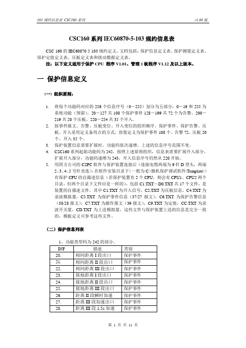
CSC160系列IEC60870-5-103规约信息表CSC-160的IEC60870-5-103规约定义,文档包括:保护信息定义表、保护测量定义表、保护定值定义表、压板定义表和扰动数据定义表。
注:以下定义适用于保护CPU 程序V1.01、管理1板程序V1.12及以上版本。
一保护信息定义(一) 组织原则:1.将每个功能码对应的256个信息序号(0-255)划分为五部分,0-19和255为系统功能(预留),20-127共108个保护事件128-199共72个为告警,200-219共20个压板,220-254共35个开入。
2.按事件报文、告警、压板变位、开入变位的组织顺序。
保护事件、保护告警、压板、开入采用定义备用点的方式,容量定义为保护事件108个、告警72、压板20个、开入35个。
3.保护装置信息需要扩展时,功能码依次递增,上述的信息序号范围不变。
4.CSC160系列起始功能码为242,按照上述原则组织,信息表需要扩展开入部分。
扩展开入部分,功能码递增为243,开入信息序号仍然从220开始。
5.用四方公司的CSPC软件与保护装置连接后(连接电缆两端为9针D型头,两端2、3、4、5号针直连),在软件安装目录下(一般为C:\微机保护调试软件\Template\)有保护CPU的自描述信息(若保护装置有2个CPU,则会有CPU1、CPU2两个目录,但两个目录下文件应是一样的),包括C1.TXT~D0.TXT共17个文件,是装置的自描述文件,其中C1.TXT为开入信号,C2.TXT为压板信息,C4.TXT为录波模拟量,C5.TXT为保护事件信息(37/27报文),C6.TXT为保护告警信息(38/28报文),C7.TXT为操作报文(39报文),C9.TXT为定值,CC.TXT为录波开关量,CD.TXT为上送模拟量,这些文件与保护装置上送的信息是完全一致的,模板定义可参考这些文件。
(二)保护信息列表续表:以下信息类别为开入信息,不同装置信息定义不同。
欧美电子产品数据手册说明书

Eaton 167706Eaton Moeller series xEffect - FRCmM-NA RCCB. Residual currentcircuit breaker (RCCB), 40A, 4p, 30mA, type G/A, UL, 110VGeneral specificationsEaton Moeller series xEffect - FRCmM-NA RCCB167706FRCMM-40/4/003-G/A-NA-110401508164247280 mm71 mm70 mm0.32 kg RoHS conformUL 1053ÖVE E 8601 IEC/EN 61008 EN45545-2 IEC 61373Additionally protects against special forms of residual pulsating DC which have not been smoothed.Product Name Catalog NumberModel CodeEAN Product Length/Depth Product Height Product Width Product Weight Compliances Certifications Catalog Notes40 AIs the panel builder's responsibility. The specifications for the switchgear must be observed.7035-35 °CMeets the product standard's requirements.Is the panel builder's responsibility. The specifications for the switchgear must be observed.DIN railQuick attachment with 2 latch positions for DIN-rail IEC/EN 6071540 ADoes not apply, since the entire switchgear needs to be evaluated.0.03 A100 V AC - 210 V AC, 94 V AC - 132 V AC (UL)Meets the product standard's requirements.Short time-delayed8 ms delay at 60 Hz10 ms delay at 50 HzInterlocking device500 A eaton-rcd-application-guide-br019003en-en-us.pdfUL 1053 DIN Rail RCCBEaton's Volume 4—Circuit Protectioneaton-xeffect-industrial-switchgear-range-catalog-ca003002en-en-us.pdf eaton-xeffect-frcmm-na-rccb-catalog-ca003019en-en-us.pdfDA-DC-03_FRCmeaton-circuit-breaker-xeffect-frcmm-na-rccb-dimensions.epsMA180503312DA-CD-f9_ul1053_4pDA-CS-f9_ul1053_4pEaton Specification Sheet - 167706eaton-circuit-breaker-xeffect-frcmm-rccb-wiring-diagram-002.eps eaton-xeffect-frcmm-rccb-wiring-diagram-002.jpgRated operational current for specified heat dissipation (In) 10.11 Short-circuit ratingRAL-numberPermitted storage and transport temperature - min10.4 Clearances and creepage distances10.12 Electromagnetic compatibilityMounting MethodAmperage Rating10.2.5 LiftingRated fault current - maxTest circuit range10.2.3.1 Verification of thermal stability of enclosures Tripping timeFitted with:Rated residual making and breaking capacity Application notesBrochuresCatalogsCertification reports DrawingsInstallation instructions mCAD model Specifications and datasheets Wiring diagramsFrequency rating50 Hz / 60 Hz10.8 Connections for external conductorsIs the panel builder's responsibility.Fault current rating30 mATerminal protectionFinger and hand touch safe, DGUV VS3, EN 50274Special featuresFRCmM-NA-110Residual current circuitbreakersType G/A (ÖVE E 8601)Sensitivity typePulse-current sensitiveAmbient operating temperature - max40 °CHeat dissipation per pole, current-dependent3.275 WClimatic proofing25-55 °C / 90-95% relative humidity according to IEC 60068-2Built-in depth70.5 mmShort-circuit ratingMax. admissible back-up fuse: 63 A gG/gL, 70 A class J fuse (UL)FeaturesResidual current circuit breakerAdditional equipment possibleLifespan, electrical4000 operationsTerminal capacity (cable)M5 (with cross-recessed screw as defined in EN ISO 4757-Z2, PZ2)Connectable conductor cross section (solid-core) - min1.5 mm²Contact position indicator colorRed / green10.9.3 Impulse withstand voltageIs the panel builder's responsibility.Number of polesFour-poleTerminal capacity (solid wire)1.5 mm² - 35 mm²Ambient operating temperature - min-25 °C10.6 Incorporation of switching devices and componentsDoes not apply, since the entire switchgear needs to be evaluated.Rated short-circuit strength5 kA (UL, as per CSA)10 kA with back-up fuse10.5 Protection against electric shockDoes not apply, since the entire switchgear needs to be evaluated.Used withFRCmM-NA-110Type G/A (�VE E 8601)Residual current circuit breakersMounting positionAs requiredEquipment heat dissipation, current-dependent13.1 W10.13 Mechanical functionThe device meets the requirements, provided the information in the instruction leaflet (IL) is observed.10.2.6 Mechanical impactDoes not apply, since the entire switchgear needs to be evaluated.10.9.4 Testing of enclosures made of insulating materialIs the panel builder's responsibility.ApplicationSwitchgear for 110-V systems10.3 Degree of protection of assembliesDoes not apply, since the entire switchgear needs to be evaluated.Voltage rating (IEC/EN 60947-2)110/190 VVoltage typeACTerminal capacity (stranded cable)16 mm² (2x)Leakage current typeAFrame45 mmBuilt-in width (number of units)70 mm (4 SU)Terminals (top and bottom)Lift terminalsAmbient humdity range5 - 95 %Impulse withstand current3 kA (8/20 μs) surge-proofWidth in number of modular spacings410.2.3.2 Verification of resistance of insulating materials to normal heatMeets the product standard's requirements.10.2.3.3 Resist. of insul. mat. to abnormal heat/fire by internal elect. effectsMeets the product standard's requirements.Lifespan, mechanical10000 operationsStatus indicationWhite / blue10.9.2 Power-frequency electric strengthIs the panel builder's responsibility.Connectable conductor cross section (solid-core) - max35 mm²Degree of protectionIP20, IP40 with suitable enclosureIP20Rated short-time withstand current (Icw)10 kAOvervoltage tested - max530 VPollution degree210.7 Internal electrical circuits and connectionsIs the panel builder's responsibility.Connectable conductor cross section (multi-wired) - min 1.5 mm²Rated impulse withstand voltage (Uimp)4 kV10.10 Temperature riseThe panel builder is responsible for the temperature rise calculation. Eaton will provide heat dissipation data for the devices.FunctionsShort-time delayed trippingVoltage rating (UL)208/120 V, 60 HzConnectable conductor cross section (multi-wired) - max 16 mm²TypeCurrent test marks as perinscriptionMaximum operatingtemperature is 75 °C:Starting at 40 °C, the max.permissible continuouscurrent decreases by 2.5%for every 1 °CThe maximum operatingcurrent of back-up fuse mustnot exceed the residualcurrent circuit breaker'srated operational current10.2.2 Corrosion resistanceMeets the product standard's requirements.10.2.4 Resistance to ultra-violet (UV) radiationMeets the product standard's requirements.10.2.7 InscriptionsMeets the product standard's requirements.Eaton Corporation plc Eaton House30 Pembroke Road Dublin 4, Ireland © 2023 Eaton. All Rights Reserved. Eaton is a registered trademark.All other trademarks areproperty of their respectiveowners./socialmedia3 kA60 °C40 A gG/gL0.03 A 22 mA190 V440 VSurge current capacity Permitted storage and transport temperature - max Admissible back-up fuse overload - max Rated fault current - min Pick-up current Rated operational voltage (Ue) - max Rated insulation voltage (Ui)。
C-D开头的集成电路
CXA1571S 射频聚焦伺服信号处理集成电路
CXA1587S 色度、同步及行场扫描信号处理集成电路
CXA1622 音频功率放大集成电路
CXA1644P 回声效果发生集成电路
CXA1645M 三基色编码集成电路
CXA1649M 低音提升集成电路
CH7201 视频编码集成电路
CHT0406 微处理集成电路
CHT0606 微处理集成电路
CHT0803 微处理集成电路
CHT0807 微处理集成电路
CHT0808 微处理集成电路
CHT0818 微处理集成电路
CIC1240A 电子振铃集成电路
CIC9106 振铃集成电路
CIC9145 音频、脉冲拨号集成电路
CKP1001S 微处理集成电路
CKP1003S 微处理集成电路
CKP1004S 微处理集成电路
CKP1006S 微处理集成电路
CKP1008S 微处理集成电路
CKP1009S 微处理集成电路
CKP1101S 微处理集成电路
CKP1103S 微处理集成电路
CKP1105S 微处理集成电路
CT54198 双向移位寄存集成电路
CT54251 数据选择8输入集成电路
CT54283 计数4位二进制集成电路
CT5430 与非门8输入集成电路
CT5440 与非门双4输入缓冲集成电路
CT5442 译码4-10线集成电路
CT54H00 与非门四2输入集成电路
CT54H01 与非门四2输入集成电路
CM006CF 数字会聚校正集成电路
HLP-A100系列通用型矢量变频器使用说明书

系列
1 1 2 2 3 4 4 5 6 9 9 9 9 9 11 11 11 12 13 17 18 18 18 19 20 22 23 24 25 48 48
系列
6.2 第01组参数:负载/电动机
ห้องสมุดไป่ตู้
52
6.3 第02组参数:制动功能
61
6.4 第03组参数:设定值/加减速
63
6.5 第04组参数:极限/警告设置
43
代表电压等级为三相380V;
P20
代表IP等级为IP20;
X
不带交流电抗器;
A
带交流电抗器;
X
不带制动单元;
B
带制动单元;
X
不带直流电抗器;
D
带直流电抗器;
1
附带有数码管显示且带电位器的操作面板;
C
PCB上涂有三防漆;
X
工厂保留;
0
销往国内;
1
销往国外;
XXX
工厂保留;
VXXX
表示软件版本号,如V235表示版本号为V2.35;
内部故障或保护。 ● 请勿自行拆装更改变频器内部连接线或零部件。 ● 严禁私自改装,更换控制板及零部件,否则有触电,发生爆炸等
危险。 ● 请防止儿童或无关人员接近变频器。
1.2 送电中
危险
● 送电中绝不可插拔变频器上的任何连接器(操作面板除外),以 避免变频器损坏并造成人员伤亡。
● 送电前请盖好面盖,以防触电,造成人身伤害。
HLP-A100系列使用说明书
系列
危险
● 实施配线前,请务必切断电源。 ● 请将变频器安装于金属类等不可燃材料上,以防止发生火灾。 ● 请不要把变频器安装在含有易燃易爆气体的环境里,否则有引
433196中文资料
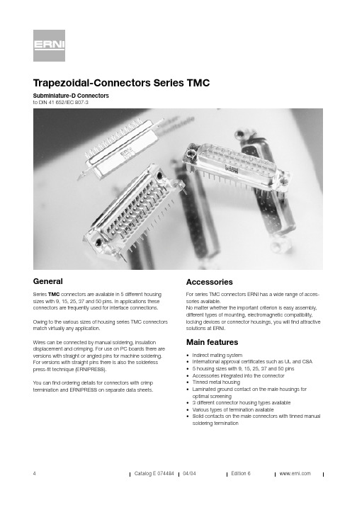
Trapezoidal-Connectors Series TMCGeneralSeries TMC connectors are available in 5 different housing sizes with 9, 15, 25, 37 and 50 pins. In applications these connectors are frequently used for interface connections.Owing to the various sizes of housing series TMC connectors match virtually any application.Wires can be connected by manual soldering, insulation displacement and crimping. For use on PC boards there are versions with straight or angled pins for machine soldering. For versions with straight pins there is also the solderless press-fit technique (ERNIPRESS).You can find ordering details for connectors with crimp terminiation and ERNIPRESS on separate data sheets.AccessoriesFor series TMC connectors ERNI has a wide range of acces-sories available.No matter whether the important criterion is easy assembly, different types of mounting, electromagnetic compatibility, locking devices or connector housings, you will find attractive solutions at ERNI.Main features•Indirect mating system•International approval certificates such as UL and CSA • 5 housing sizes with 9, 15, 25, 37 and 50 pins •Accessories integrated into the connector•Tinned metal housing•Laminated ground contact on the male housings for optimal screening• 3 different connector housing types available•Various types of termination available•Solid contacts on the male connectors with tinned manual soldering terminationSubminiature-D Connectors to DIN 41 652/IEC 807-3D-Sub TerminationPerformance Levels207to DIN 41 652/IEC 807-3MIL-C-24308, CCTU 08-14and IEC-Recommendation 48 B200 mating cyclesContact zone gold-platedterminal zone tinned201as for version 207 butterminal zone gold-plated 107to DIN 41 652/IEC 807-3MIL-C-24308, CCTU 08-14and IEC-Recommendation 48 B500 mating cyclesContact zone gold-platedterminal zone tinned101as for version 107 butterminal zone gold-platedPerformance level 107and101connectors are available on request.Approval CertificatesUL All male and female connectors from this data sheet are approved by the American certification authority …Under-writers Laboratories Inc.“.File no. E 84703CSA All types are listed by the Canadian certification author-ity …Canadian Standards Association“.File Nr. LR 62503 and LR 62504.For ERNIPRESS, crimping and insulation displacement (IDC)there are separate data sheets available.Integrated AccessoriesRiveted nut (see fig. 1)On the version with riveted nut there is a nut riveted into the mounting flanges of the connector so that it cannot twist. The thread is available as a M3 and 4/40" version. This facilitates fitting into housings or front panels.Threaded bolt (see fig. 2)To ensure secure connector locking, a screw locking device is frequently used with threaded bolts. TMC connectors from ERNI are available with riveted threaded bolts. These hexagon bolts are available with internal threads of M3 and 4/40". For the user it means there is no need for loose accessories.Spacer bolt (see fig. 3)Due to the design of the TMC connectors a spacer is required for vertical assembly on pc boards. These parts are supplied by ERNI as individual accessories.Ground pin (see fig. 4)The additional ground pin is designed for connecting up to the pc board chassis contact for example.Spacer bolt with mounting clip (on request)(see fig. 5)These spacer bolts can be snapped into the mounting holes on the pc board. If the holes are plated-through there will also be a solder joint.Ground clip (see fig. 6)For screening contact there are angled ERNI TMC connector ground clips available. These clips are soldered into the mounting holes on the pc board, thus creating a firm chassis connection.Ground bar (see fig. 7)Ground bars on angled connectors are attached to the guide frame on the pc board. This makes it possible to make connection with chassis conductors on the pc board.Ground eyelet (on request) (see fig. 8)With the ground lug the chassis contact can be soldered on.D-Sub Tinned metal housings andlaminated ground contactsThe metal housings on the TMC connectors (standardversions) from ERNI are tinned so as to achieve better contactfor the chassis connection. Specially punched grooves on themetal protective collar of the male connectors ensure reliable contact. Together with the ERNI connector housings in the metallized version and grounding accessories on the connec-tors an optimal electromagnetically compatible application is achieved.Solid punched male contactsDue to a special manufacturing process we are in a positionto offer solid punched male contacts.These versions have a tinned terminal zone and are suitablefor a current-carrying capacity of up to 7.5 A.Guide frame for angled connectorsFor mounting purposes and better guidance of angled TMC connectors with pins for dip-soldering the standard versionsare equipped with a guide frame made of plastic.With this guide frame the connectors can be screwed orriveted onto pc boards.Versions with a guide frame and mounting clip are clipped intothe pc boards and soldered in place.Connector housings for TMC connectorsERNI has also developed connector housings for series TMC interface connectors.• KSG 183housing with engagement locking• KSG 184housing with slide locking• KSG 185housing with engagement and/or screwlocking, integrated codingThese two-shell connector housings are also available inmetallized versions. Together with the ERNI TMC connectors,which have laminated ground contacts, screening is optimized.Versions Numbers of pins 2-rows of 9, 15, 25, 37 and 3-rows of 50 contactsTemperature range -65°...+125°CPermissible humidity Annual average ≤80%, max. 100%Creepage and clearance ≥1,0 mmWorking current 7,5 A max. 5 A max.Test voltage 1250 V rms 1000 V rms Contact resistance ≤2,5 m Ω≤10 m ΩInsulation resistance≥1014ΩShock and vibration proofness No discontinuity at 20 g and 10...2000 HzShock proofness up to 50 gMetal protective collar Tinned steelMR St 4, 1+1 µm Ni, 8±2 µm SNMouldingPBT 30% GVInflammability of the plastic Non flammable as per UL 94 V-0Comperative creepagefigure to CTI 275 / CTI 175 MDIN IEC 112 for PBT Service lifePerformance Level 2 ≥250 mating-cyclesContact force perfemale element0,4 NTMC-male connectors to PerformanceLevels 207 and 201TMC-female connectors to Performance Levels 201TMC-female connectors to Performance Level 207Example of how to orderElectrical and mechanical data023122023123023124023125023126*Dimension tablesPin connectors (P)D-Sub Socket connectors (S)Termination for the versions listed in this data sheetLoe= Solder eyelet tinned (male connector)L= Solder cupTL= Straight solder pin termination for print assemblyLP= Angled solder pin termination for print assembly (with and without guide frame)W= Wire-wrap terminationContact identification (wiring side)9 pins15 pins25 pins37 pins50 pinP S P S P S P S P STMC with manual soldering terminationDimensional drawingsMale connector Female connectorOrdering details004617004620004613004926004615023127023128023129023130023131*004125013522013635004633013844D-SubAssembly detailsTMC with manual solder terminationAssembly cutoutFront assemblyRear assemblyZone of reliable contactTMC with straight dip-solder termination Dimensional drawingsMale connectorFemale connectorDimensional drawings023132023133023019023134023135* 023136023137023138023139023140* 023141023142023143023144023145* 023146023147023148023149023150* 023151023152023153023154023155*003552003553003554003555013920 003634013052003625013702013897 003633013551003626013701013898 003635013550003628013700013892 003636013549003627013699013893Assembly detailsTMC with straight dip-solder terminationPC board hole patterns9 – 37 pin 50 pinSpacer sleeve(available as integrated accessory)PC board Zone of reliablecontact023156023157023158023159023160*013032013033013029013034013641D-SubTMC with straight dip-solder termination (with guide frame)Dimensional drawingsMale connectorFemale connectorOrdering details023166023167023168023169023170*003644004154003643004153013922023171023172023173023174023175*003599013533003622013707013894023181023182023183023184023185*003600013535003623013710013899023186023187023188023189023190*003601013534003624013709013900023176023177023178023**********003598013532003621013708013895D-Sub 023191023192023193023194023195*023196023197023198023199023200023201023202023203023204023205*023206023207023208023209023210023249023250023251023252023253*023279023280023281023282023283 023211023212023213023214023215*023254023255023256023257023258 023216023217023218023219023220*013973434287023259023260023261 023221023222023223023224023225*023262023263023264023265023266 023226023227023228023229023230*003585004225003608023367023268 023284023285023286023287023288*003584013541003464023304023305 023289023290023291023292023293*003583004925003606023306434705 433196023231023232023233023234*433197023049023082023269023270 023235023236023237023238023239*023104023271023272023273023274For further accessories and other combination options please consult ERNI’s local office sales. Assembly detailsTMC with straight dip-solder terminationPC board hole patterns9 – 37 pin 50 pinPC boardZone of reliablecontact013966023240023241023242023243023244023245023246023247023248*023294023295023296023297023298*023299023300023301023302023298*013965023275003605023276004869003581013542013834023277023278003579013014023307004448023308003580023309003603023310023311D-SubSpecial version with solder pitch of 2.84 mm between the rows TMC with angled dip-solder termination (solder pitch 2.84 mm)Dimensional drawingsMale connectorFemale connectorOrdering details about special version with solder pitch of 2.84 mmDue to the wider pitch between the rows, there is more space for conductors on the PC board. The clearance and creepage ages are greater on these versions.PC board hole patterns9 – 37 pin023317023318023319023320023*********TMC with angled dip-solder termination (without guide frame)Dimensional drawingsMale connectorFemale connectorOrdering detailsIntegrated accessories are also available on request for TMC connectors with angled terminals without guide frame.For assembly, an assembly comb is available on request.023322023323023324023325023326*013487013525013624013714013930D-SubAssembly detailsTMC with angled dip-soldered termination without guide framePC board hole patterns9 – 37 pin50 pinPC boardZone of reliable contactPC boardTMC with wire wrap terminations Dimensional drawingsMale connectorFemale connectorOrdering detailsScrew locking accessories (for all TMC standard version connectors)Ordering details434831434832434833434830023327023328023329023330023331*013492013553013632013698013928。
MAX1036-MAX1039资料
MAX1036–MAX1039
Applications
Hand-Held Portable Applications Medical Instruments Battery-Powered Test Equipment Solar-Powered Remote Systems Received-Signal-Strength Indicators System Supervision
Stresses beyond those listed under “Absolute Maximum Ratings” may cause permanent damage to the device. These are stress ratings only, and functional operation of the device at these or any other conditions beyond those indicated in the operational sections of the specifications is not implied. Exposure to absolute maximum rating conditions for extended periods may affect device reliability.
ELECTRICAL CHARACTERISTICS
(V DD = 2.7V to 3.6V (MAX1037/MAX1039), V DD = 4.5V to 5.5V (MAX1036/MAX1038). External reference, V REF = 2.048V (MAX1037/MAX1039), VREF = 4.096V (MAX1036/MAX1038). External clock, fSCL = 1.7MHz, TA = TMIN to TMAX, unless otherwise noted. Typical values are at TA = +25°C.)
PS11036中文资料

Powerex, Inc., 200 Hillis Street, Youngwood, Pennsylvania 15697-1800 (724) 925-7272Intellimod™ ModuleApplication Specific IPM 30 Amperes/600 VoltsPS11036Description:Powerex Application Specific IPMs (ASIPMs) are inteligent power modules that integrate powerdevices, gate drive and protection circuitry in a compact package for use in small inverter applications up to 20kHz. Use of application specific HVICs allow the designer to reduce inverter size and overall design time.Features:□Compact Packages□3 Phase Converter Bridge Built-in□Integrated HVICs□Direct Connection to DSP/CPU Applications:□Small Motor Control □Small Servo Motors□General Purpose Inverters□Pump and HVAC Motor Control Ordering Information:PS11036 is a 600V , 30 Ampere Application SpecificIntelligent Power Module.DimensionsInches Millimeters A 3.74±0.0495.0±1.0B 2.91±0.0474.0±1.0C 0.32±0.028.0±0.5D 3.35±0.01285.0±0.3E 2.45±0.0362.35±0.8F 1.2431.6G 0.5714.5H 2.2056.0J 0.08 2.0K 0.9424.0L 0.7118.0M 0.020.4N 0.5915.0P 0.359.0Q 2.32±0.01259.0±0.3R1.3835.0DimensionsInches MillimetersS 0.10 2.5T 2.8071.0U 3.2382.1V 0.020.5W 0.25±0.012 6.35±0.3X 2.25±0.0357.15±0.8Y 0.08 2.0Z 0.14 3.5AA 0.65±0.0216.5±0.5BB 0.12±0.02 3.0±0.5CC 0.9323.5DD 1.21±0.0230.75±0.5EE 0.181 Dia. 4.6 Dia.FF 0.197 Dia. 5.0 Dia GG 0.020.5HH0.164.0Outline Drawing and Circuit DiagramPowerex, Inc., 200 Hillis Street, Youngwood, Pennsylvania 15697-1800 (724) 925-7272PS11036Intellimod™ ModuleApplication Specific IPM30 Amperes/600 VoltsAbsolute Maximum Ratings, T j = 25°C unless otherwise specifiedCharacteristics Symbol PS11036Units Power Device Junction T emperature*T j-20 to 125°C Storage Temperature T stg-40 to 125°C Case Operating Temperature (See T C Measure Point Illustration)T C-20 to 100°C Mounting Torque, M4 Mounting Screws—13in-lb Module Weight (Typical)—105Grams Isolation Voltage**V ISO2500Volts *The indicated values are specified considering the safe operation of all the parts within the ASIPM. The maximum rating for the ASIPM power chips (IGBT & FWDi) is T j < 150.**60 Hz sinusoidal AC applied between all terminals and the base plate for 1 minute.IGBT Inverter SectorSupply Voltage (Applied between P2 - N2)V CC450Volts Supply Voltage, Surge (Applied between P2 - N2, Surge-Value)V CC(surge)500Volts Each IGBT Collector-Emitter Static Voltage (Applied between P2-U.V.W, U.V.W-N2)V P or V N600Volts Each IGBT Collector-Emitter Switching Voltage V P(S) or V N(S)600Volts (Applied between P2-U.V.W, U.V.W-N2 (Pulse))Each IGBT Collector Current, T C = 25°C, “( )” means I C Peak Value±I C(±I CP)±30 (±60)AmperesConverter SectorRepetitive Peak Reverse Voltage V RRM800Volts Recommended AC Input Voltage E a220Vrms DC Output Current (3-phase Rectifying Circuit)I DC30 A Surge (Non-repetitive) Forward Current (1 Cycle at 60Hz, Peak Value Non-repetitive)I FSM300AI2t for Fusing (Value for One Cycle of Surge Current)I2t375A2sControl SectorSupply Voltage V D,V DB-0.5 ~ 20Volts Input Signal Voltage V CIN-0.5 ~ 7.5Volts Fault Output Supply Voltage V FO-0.5 ~ 7.5Volts Fault Output Current I FO15mA DC-Link IGBT Current Signal Amp Output Current I AMP1mAPowerex, Inc., 200 Hillis Street, Youngwood, Pennsylvania 15697-1800 (724) 925-7272PS11036Intellimod™ ModuleApplication Specific IPM30 Amperes/600 VoltsElectrical and Mechanical Characteristics, T j = 25°C unless otherwise specifiedCharacteristics Symbol Test Conditions Min. Typ.Max.UnitsIGBT Inverter SectorCollector-Emitter Saturation Voltage V CE(sat)I C = 30A, T j = 25°C, V D = V DB = 15V,—— 2.9VoltsInput = ON (Shunt Voltage Drop Not Included)Diode Forward Voltage V EC T j = 25°C, -I C = 30A—— 2.9Volts Converter Diode Voltage V FR T j = 25°C, I FR = 10A—— 1.5Volts Converter Diode Reverse Current I RRM V R = V RRM, T j = 125°C——8mA Switching Times onC(on)CC C joff D DBC(off)on offrrShort Circuit Endurance (Output, Arm, and@V CC≤ 400V, Input = 5V → 0V (One-shot),• No DestructionLoad Short-Circuit Modes) -20°C ≤ T j(start)≤ 125°C,• F O Output by Protection Operation13.5V ≤ V D = V DB≤ 16.5VSwitching SOA @V CC≤ 400V, Input = 5V → 0V,• No DestructionT j≤ 125°C, I C < OC T rip Level,• No Protecting Operation13.5V ≤ V D = V DB≤ 16.5V• No F O OutputT C Measure PointCPowerex, Inc., 200 Hillis Street, Youngwood, Pennsylvania 15697-1800 (724) 925-7272PS11036Intellimod™ ModuleApplication Specific IPM30 Amperes/600 VoltsElectrical and Mechanical Characteristics, T j = 25°C unless otherwise specifiedCharacteristics Symbol Test Conditions Min. Typ.Max.UnitsControl SectorCircuit Current (Average)I D T j = 25°C, V D = 15V, V IN = 5V——50mAI DB T j = 25°C, V D = V DB = 15V, V IN = 5V——5mA Input ON Threshold Voltage V th(on)0.8 1.4 2.0Volts Input OFF Threshold Voltage V th(off) 2.5 3.0 4.0Volts Input Pull-up Resistor Ri Applied between—50—kΩInput Terminal-inside Power SupplyPWM Input Frequency f PWM T C≤ 100°C, T j≤ 125°C1—15kHz Arm Shoot-through Blocking Time*t DEAD Relates to Corresponding Inputs 2.2——µST C = -20°C ~ 100°CInput Interlock Sensing t int Relates to Corresponding Input—100—ns Inverter DC-link IGBT Current V amp 100%I C = I OP(100%), V D = 15V, T j = 25°C 1.5 2.0 2.5Volts Sense Voltage Output Signal** V amp 200%I C = I OP(200%), V D = 15V, T j = 25°C 3.0 4.0 5.0Volts Inverter DC-link IGBT Current V amp 250%I C = I OP(250%), V D = 15V 5.0——Volts Sense Voltage Output Limit** V amp 0%I C = I OP(0%), V D = 15V—50100mV Over-Current Trip Level OC31.139.060.0AmperesOC jShort-Circuit Trip Level SC—60—AmperesSCTrip Level UV D11.012.013.0Volts Supply Circuit Reset Level UV Dr11.512.513.5Volts Under-Voltage DB C jProtection Reset Level UV DBr10.611.312.1Volts Delay Time t dV—10—µS Fault Output Pulse Width***t FO T j = 25°C 1.0 1.8—mS Fault Output Current***I Fo(H)Open Collector Output——1µAFo(L)* The dead-time has to be set externally by the CPU; it is not part of the ASIPM internal functions.**Refer ro the graph on next page.***Fault output signalling is given only when the internal OC, SC, and UV protection circuits are activated. The OC, SC and UV protection (and fault output) operate for the lower arms only. The OC and SC protection fault output is given in a pulse format while that of UV protection is maintained thrpughout the duration of the under-voltage condition.PS11036Intellimod ™ ModuleApplication Specific IPM 30 Amperes/600 VoltsPowerex, Inc., 200 Hillis Street, Youngwood, Pennsylvania 15697-1800 (724) 925-7272Thermal CharacteristicsCharacteristic Symbol Condition Min. Typ.Max.Units Junction to CaseR th(j-c)Q Each IGBT —— 1.5°C/Watt R th(j-c)D Each FWDi —— 2.4°C/Watt R th(j-c)DREach Converter —— 2.0°C/Watt Contact Thermal ResistanceR th(c-f)Case to Fin Per Module.——0.042°C/WattThermal Grease AppliedRecommended Conditions for UseCharacteristic Symbol ConditionMin.Typ.Value Units Supply Voltage V CCApplied across P2-N2 Terminals —300400Volts Control Supply VoltageV D Applied between V D -GND 13.515.016.5Volts V DBApplied between CBU+ & CBU-,13.515.016.5VoltsCBV+ & CBV-, CBW+ & CBW-Control Supply dv/dt dV D /dt, dV DB /dt-1—1V/µs Input ON Voltage V CIN(on)Applied between 0—0.8Volts CIN(off)P P P N N N Module Case Operating Temperature T C ——100°C PWM Input Frequencyf PWM T C ≤ 100°C, T j ≤ 125°C ——15kHz Allowable Minimum Input On-pulse Width t XX 1——µS Arm Shoot-through Blocking Timet DEADRelate to Corresponding Inputs2.2——µSC U R R E N T S E N SE V O L T A G EO U T P U T S I G N A L ,V A M P , (V O L T S )INVERTER DC-LINK IGBT CURRENT ANALOG SIGNALING (TYPICAL)510020043210300ACTUAL LOAD PEAK CURRENT, (%), (I C = I O X ͌2 )PS11036Intellimod ™ ModuleApplication Specific IPM 30 Amperes/600 VoltsPowerex, Inc., 200 Hillis Street, Youngwood, Pennsylvania 15697-1800 (724) 925-72722112–+–+–+V DU P V P W U N V N W F V Functional Block Diagram。
富马酸卢帕他定的液态制剂[发明专利]
![富马酸卢帕他定的液态制剂[发明专利]](https://img.taocdn.com/s3/m/e512d38a1b37f111f18583d049649b6648d709e3.png)
(10)申请公布号 (43)申请公布日 2013.05.15C N 103108635 A (21)申请号 201180030947.1(22)申请日 2011.06.3010382184.9 2010.06.30 EP61/364,992 2010.07.16 USA61K 31/4545(2006.01)A61K 9/00(2006.01)A61K 9/08(2006.01)A61K 47/10(2006.01)G01N 30/02(2006.01)A61P 11/02(2006.01)A61P 11/04(2006.01)A61P 37/08(2006.01)(71)申请人J·乌里亚奇·Y 股份有限公司地址西班牙巴塞罗那(72)发明人M·索雷欧·费勒S·莫尔里森·卡普德维拉(74)专利代理机构北京市浩天知识产权代理事务所 11276代理人雒纯丹 刘倞芳(54)发明名称富马酸卢帕他定的液态制剂(57)摘要本发明提出富马酸卢帕他定的无环糊精含水液态制剂,其可用于治疗过敏性鼻炎及荨麻疹。
所述制剂包含富马酸卢帕他定、一种或多种共溶剂及一种或多种pH 调节剂,其中该组合物的pH 介于4与6.5之间。
(30)优先权数据(85)PCT申请进入国家阶段日2012.12.21(86)PCT申请的申请数据PCT/EP2011/060994 2011.06.30(87)PCT申请的公布数据WO2012/001093 EN 2012.01.05(51)Int.Cl.权利要求书3页 说明书13页(19)中华人民共和国国家知识产权局(12)发明专利申请权利要求书3页 说明书13页(10)申请公布号CN 103108635 A*CN103108635A*1.一种无环糊精含水液态药学组合物,其包含:-富马酸卢帕他定,-一种或多种共溶剂,及-一种或多种pH调节剂,其中该组合物的pH介于4与6.5之间。
线路保护规程四方CSC-103c(参考其说明书)(仅供参考)

1线路保护1.1技术参数1.1.1环境条件装置在以下环境条件下能正常工作:(1)工作环境温度:-10℃~+55℃。
运输中短暂的贮存环境温度-25℃~+70℃,在极限值下不施加激励量,装置不出现不可逆的变化,温度恢复后,装置应能正常工作;(2)相对湿度:最湿月的月平均最大相对湿度为90%,同时该月的月平均最低温度为25℃且表面无凝露;(3)大气压力:80kPa~110kPa;(4)使用场所不得有火灾、爆炸、腐蚀等危及装置安全的危险和超出本说明书规定的振动、冲击和碰撞。
1.1.2额定参数(1)交流电压U n:100/ 3 V;线路抽取电压U x:100V 或100/ 3 V;(2)交流电流I n:5A ,1A;(3)交流频率: 50Hz;(4)直流电压: 220V,110V;(5)开入输入直流电压:24V(默认),也可以选择220V 或110V。
1.1.3交流回路精确工作范围(1)相电压: 0.25V~70V ;(2)检同期电压: 0.4V~120V ;(3)电流: 0.08I n~30I n。
1.1.4差动元件(1)整定范围: 0.1I n~2I n;级差0.01A;(2)整定值误差:不大于±2.5% 或±0.02 I n;(3)动作时间: 2 倍整定值时,不大于20ms。
1.1.5距离元件(1)整定范围:0.01Ω~40Ω(5A);0.05Ω~200Ω(1A);级差0.01Ω;(2)距离I 段的暂态超越:不大于±4%;(3)距离I 段动作时间:近处故障不大于15ms;(4)0.7 倍整定值以内时,不大于20ms;(5)测距误差(不包括装置外部原因造成的误差)(6)金属性短路故障电流大于0.01 I n 时,不大于±2%,有较大过渡电阻时测距(7)误差将增大。
1.1.6零序方向过流元件(1)整定范围:0.1I n ~20I n;级差0.01A;(2)零序I 段的暂态超越:不大于±4%。
柯尼卡美能达 EP1031 中文简易说明书
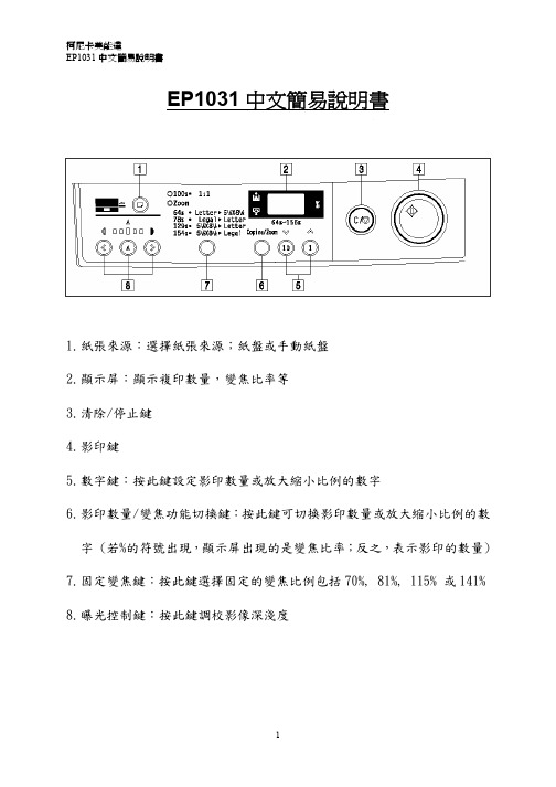
EP1031中文簡易說明書
1.紙張來源:選擇紙張來源;紙盤或手動紙盤
2.顯示屏:顯示複印數量,變焦比率等
3.清除/停止鍵
4.影印鍵
5.數字鍵:按此鍵設定影印數量或放大縮小比例的數字
6.影印數量/變焦功能切換鍵:按此鍵可切換影印數量或放大縮小比例的數
字 (若%的符號出現,顯示屏出現的是變焦比率;反之,表示影印的數量)
7.固定變焦鍵:按此鍵選擇固定的變焦比例包括70%, 81%, 115% 或141%
8.曝光控制鍵︰按此鍵調校影像深淺度
故障訊號Error Message
1.此訊號表示需加碳粉,請致電2565 2139 訂購碳粉
2.此訊號表示需要進行定期維修保養,請致電2565 2177聯絡維修人員
3. 此訊號表示紙張塞紙
4. 此訊號表示紙盤沒有紙或塞紙
1.影像濃度 Image Density
z按此鍵手動調校影像深淺
z按此鍵進入自動曝光模式,影印機會根據原稿的濃度自動調節深淺
2.設定影印數量 Copy Quantity
做法:如影印23張副本,按數字鍵 (10) 兩次和 (1) 三次
3. 調整變焦比率
做法1:選擇固定變焦比率
做法
I.
先按影印數量/變焦功能切換鍵
II. 按數字鍵 ︽增加1%或減少 ︾ 1%
按此鍵後,%符號閃亮,如左圖
按此鍵使倍率以1%遞增或遞減,最少為64%,最大為156%
4. 總影印張數
z檢查咪錶讀數可按清除鍵大概3秒放手
z顯示屏不停閃爍跳動,然後出現三組兩位數字,例如:12,345張,出現的次
序如下,01, 23, 45 (請參考圖一)
圖一。