APL5336KAI-TRL中文资料
APM4435KC-TRL中文资料
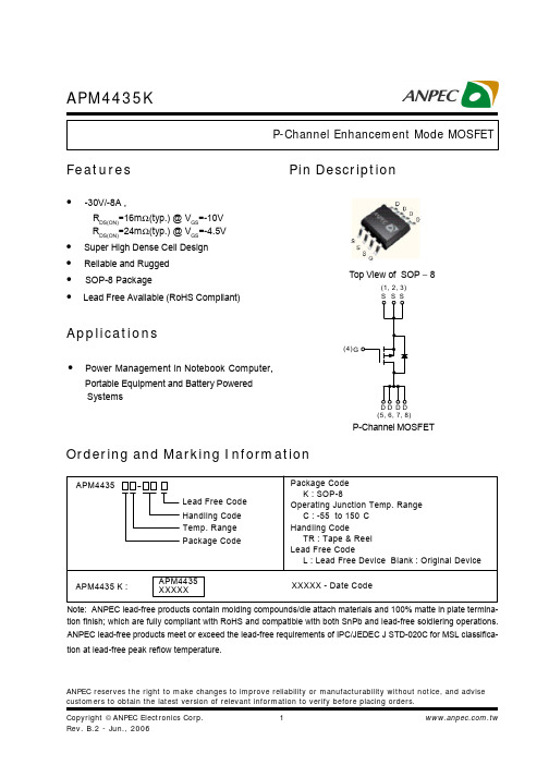
ANPEC reserves the right to make changes to improve reliability or manufacturability without notice, and advise customers to obtain the latest version of relevant information to verify before placing orders.APM4435KFeaturesApplications• Power Management in Notebook Computer,Portable Equipment and Battery Powered SystemsPin DescriptionOrdering and Marking InformationP-Channel MOSFETAPM4435Handling Code Temp. Range Package CodePackage Code K : SOP-8Operating Junction Temp. Range C : -55 to 150C Handling CodeTR : Tape & Reel Lead Free CodeL : Lead Free Device Blank : Original Device APM4435 K :XXXXX - Date CodeLead Free Code APM4435XXXXX• -30V/-8A ,RDS(ON)=16m Ω(typ.) @ VGS =-10VRDS(ON)=24m Ω(typ.) @ V GS =-4.5V• Super High Dense Cell Design • Reliable and Rugged • SOP-8 Package•Lead Free Available (RoHS Compliant)Top View of SOP − 8G(4)(1, 2, 3)(5, 6, 7, 8)Note: ANPEC lead-free products contain molding compounds/die attach materials and 100% matte in plate termina-tion finish; which are fully compliant with RoHS and compatible with both SnPb and lead-free soldiering operations.ANPEC lead-free products meet or exceed the lead-free requirements of IPC/JEDEC J STD-020C for MSL classifica-tion at lead-free peak reflow temperature.APM4435KAbsolute Maximum Ratings (TA= 25°C unless otherwise noted)Electrical Characteristics (TA = 25°C unless otherwise noted)*Surface Mounted on 1in2 pad area, t ≤ 10sec.APM4435KElectrical Characteristics (Cont.) (T= 25°C unless otherwise noted)Aa : Pulse test ; pulse width≤300µs, duty cycle≤2%.b : Guaranteed by design, not subject to production testing.APM4435K1E-41E-30.010.1110301E-30.010.112Typical Characteristics-I D - D r a i n C u r r e n t (A )Drain CurrentT j - Junction Temperature (°C)Safe Operation Area-V DS - Drain - Source Voltage (V)Thermal Transient ImpedanceSquare Wave Pulse Duration (sec)Power DissipationP t o t - P o w e r (W )T j - Junction Temperature (°C)-I D - D r a i n C u r r e n t (A )204060801001201401600.00.51.01.52.02.5204060801001201401602468100.010.11101000.010.1110100N o r m a l i z e d T r a n s i en t T h e r m a l R e s i s t a n c e012345-50-250255075100125150 -V GS - Gate - Source Voltage (V)T j - Junction Temperature (°C)APM4435K-V DS - Drain - Source Voltage (V)Drain-Source On ResistanceN o r m a l i z e dO n R e s i s t a n c e T j - Junction Temperature (°C)C - C a p a c i t a n c e (p F )-V SD - Source - Drain Voltage (V)-I S - S o u r c e C u r r e n t (A )CapacitanceGate ChargeQ G - Gate Charge (nC)-V G S - G a t e -s o u r c e V o l t a g e (V )Typical Characteristics (Cont.)-50-252550751001251500.000.250.500.751.001.251.501.752.000.1110305101520253005001000150020002500300035004000450050005101520253035404550APM4435KPackaging InformationSOP-8 pin ( Reference JEDEC Registration MS-012)APM4435KT LT P25T e m p e r a t u r eTimeReflow Condition (IR/Convection or VPR Reflow)Classification Reflow ProfilesPhysical SpecificationsAPM4435KCarrier Tape & Reel DimensionsReliability Test ProgramClassification Reflow Profiles(Cont.)APM4435KCover Tape DimensionsCarrier Tape & Reel Dimensions(Cont.)(mm)Customer ServiceAnpec Electronics Corp.Head Office :No.6, Dusing 1st Road, SBIP,Hsin-Chu, Taiwan, R.O.C.Tel : 886-3-5642000Fax : 886-3-5642050Taipei Branch :7F, No. 137, Lane 235, Pac Chiao Rd.,Hsin Tien City, Taipei Hsien, Taiwan, R. O. C.Tel : 886-2-89191368Fax : 886-2-89191369。
敦泰触摸IC参数对照表
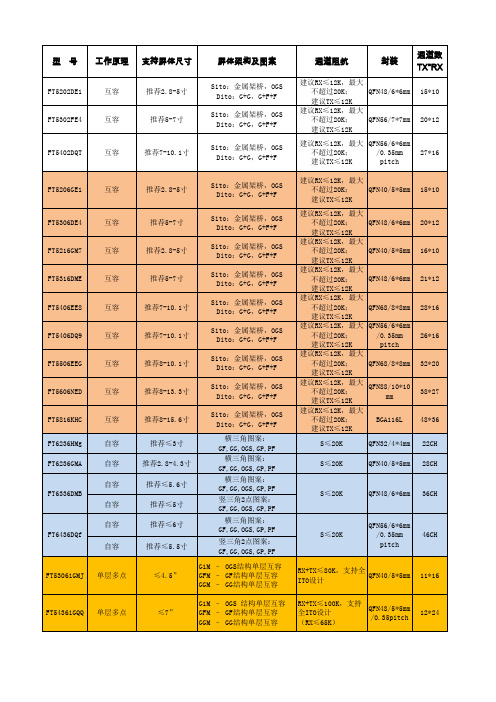
工作温度: -20~+85 储存温度: -55~+150 工作温度: -20~+70 储存温度: -55~+150
Android
FLASH
优
优
有
标准I2C
2.8~3.6V
Android
FLASH
优
优
有
标准I2C USB
2.8~3.6V
独立IOVCC
Android Win8
FLASH
优
优
--
标准I2C USB
20*12
FT5402DQT
互容
推荐7-10.1寸
27*16
FT5206GE1
互容
推荐2.8-5寸
Sito:金属架桥,OGS Dito:G+G,G+F+F Sito:金属架桥,OGS Dito:G+G,G+F+F Sito:金属架桥,OGS Dito:G+G,G+F+F Sito:金属架桥,OGS Dito:G+G,G+F+F Sito:金属架桥,OGS Dito:G+G,G+F+F Sito:金属架桥,OGS Dito:G+G,G+F+F Sito:金属架桥,OGS Dito:G+G,G+F+F Sito:金属架桥,OGS Dito:G+G,G+F+F Sito:金属架桥,OGS Dito:G+G,G+F+F 横三角图案: GF,GG,OGS,GP,PF 横三角图案: GF,GG,OGS,GP,PF 横三角图案: GF,GG,OGS,GP,PF 竖三角2点图案: GF,GG,OGS,GP,PF 横三角图案: GF,GG,OGS,GP,PF 竖三角2点图案: GF,GG,OGS,GP,PF G1M – OGS结构单层互容 GFM – GF结构单层互容 GGM – GG结构单层互容 G1M – OGS 结构单层互容 GFM – GF结构单层互容 GGM – GG结构单层互容
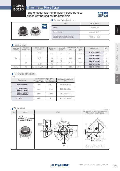
263系列金属螺杆尖耐抗电尖耐抗电尖通螺杆类型环形编码器说明书
Through shaft type
Horizontal
Horizontal
—
12/12
12/24 12/12
9/18 15/30
Ring type
— 15/30
Features
W
Dimensions (mm)
D
H
Operating temperature range
Operating life Automotive use Life cycle (availability)
300V AC for 1minute or 360V AC for 2s
300V AC for 1minute or 360V AC for 1s
—
7±5mN・m 12±5mN・m 16±7mN・m
—
17±8mN・m(Initial) 12+− 74mN・m(After reflow)
100N
Shaft configuration
1
Style
5-3.5 9
4 Mounting surface
3 2
120°
ø21.6
C ø12.2
AB 1
2-8
120°
0.7
2-10.4 120°
Unit:mm
PC board mounting hole dimensions (Viewed from mounting side)
22.3
3
˃˃
˃ $ ˃ $
˃˃
"# "#
EC21A Actuator length 15mm 9 pulse/18 detent
照相电子Photologic 传感器 OPL530-OPL563 型号说明书

Photologic ® SensorOPL530, OPL531, OPL535, OPL536, OPL550, OPL551, OPL560, OPL561, OPL562, OPL563Description:All components in this series include a photodiode, amplifier, voltage regulator, Schmitt trigger and NPN output transistor on a singlesilicon chip. OPL560 chips also include a voltage regulator on the chip. All devices in the series have a Photologic® chip that is encapsulated in a molded plastic side -looking package with an integral lens (recessed integral lens for OPL535 and OPL536). This packaging provides enhanced optical coupling, combined with mechanical protection. The hysteresis characteristics of the Schmitt trigger on each device offers high immunity to noise on input and V CC .OPL530, OPL531, OPL535 and OPL536 include a 10 K Ω pull -up resistor (R L ) from output to V CC . These components exhibit very stable performance over supply voltages ranging from 4.5 V to 16 V and a wide range of irradiance levels. OPL550 and OPL551 devices feature TTL/LSTTL compatible logic level output which can drive up to 8 TTL loads without additional circuitry and medium -speed data rates to 250 kBaud, with typical rise and fall times of 25 nanoseconds. OPL560, OPL561, OPL562 and OPL563 devices feature TTL/LSTTL compatible logic level output which can drive up to 10 TTL loads over supply voltages ranging from 4.5 V to 16 V.OPL530, OPL531, OPL550, OPL551, OPL560, OPL561, OPL562 and OPL563 are mechanically and spectrally matched to OP140 and OP240 LEDs. OPL535 and OPL536 are mechanically and spectrally matched to OP145 and OP245 series LEDs.Applications:• Non -contact reflective object sensor • Assembly line automation • Machine automation • Machine safety • End of travel sensor •Door sensorFeatures:• Choice of four output options in low -cost side -looking package • Choice of two sensitivity options (OPL560/561/562/563) • High noise immunity• Direct TTL/LSTTL CMOS interface• Data rates to 250 kBaud for all except OPL560 series (200 kBaud) • Low power consumptionRoHSOPL551, OPL560, OPL561, OPL562, OPL563OPL530, OPL550, OPL560 SeriesOPL535, OPL536 SeriesDIMENSIONS ARE IN:[MILLIMETERS] INCHESDIMENSIONS ARE IN:[MILLIMETERS] INCHESOPL551, OPL560, OPL561, OPL562, OPL563V CCOUTGND V CCOUTGND V CCOUTGNDV CCOUTGNDOPL550/550A/560/560A/562 Totem -PoleOPL551/561/563 Inverted Totem -PoleOPL531-OCA/551-OC/551-OCA/561-OC/561-OCA Inverted Open -CollectorOPL530-OC/550-OCA/560-OCA/562-OC/562-OCA Open -CollectorV CCOUTGNDV CCOUTGNDOPL531A, OPL536/536A Inverted 10K Pull -UpOPL531A/536A Inverted 10 K Pull -UpOPL551, OPL560, OPL561, OPL562, OPL563Electrical SpecificationsAbsolute Maximum Ratings (T A = 25° C unless otherwise noted)(1)RMA flux is recommended. Duration can be extended to 10 sec. max. when flow soldering. For OPL530, OPL530-OC, OPL531A, OPL531-OCA, OPL535A, OPL535B, and OPL536A a maximum of 20 grams force may be applied to leads while at soldering temperatures.(2)Derate linearly 2.67 mW/° C above 70° C for OPL530, OPL530-OC, OPL531A, OPL531-OC, OPL535A/B, and OPL536A. Derate linearly 2.5mW/° C above 25° C for all devices in the OPL550, OPL551, OPL560, OPL561, OPL562 and OPL563 series.(3)Irradiance measurements are made with λi = 935 nm.(4)This applies to OC versions only. For I CC on pull-up versions, add V CC/10 KΩ.OPL551, OPL560, OPL561, OPL562, OPL563Electrical Characteristics (T A = 25° C unless otherwise noted)Electrical SpecificationsElectrical Characteristics (T A = 25° C unless otherwise noted)Notes:(1) RMA flux is recommended. Duration can be extended to 10 sec. max. when flow soldering. For OPL530 and OPL530-OC a maximum of 20grams force may be applied to leads while at soldering temperatures.(2) Derate linearly 2.67 mW/° C above 70° C for OPL530 and OPL530-OC. Derate linearly 2.5 mW/° C above 25° C for all devices in the OPL550,OPL560, OPL561, OPL562 and OPL563 series.(3) Irradiance measurements are made with λi = 935 nm.(4) This applies to OC versions only. For I CC on pull -up versions, add V CC /10 K Ω.OPL551, OPL560, OPL561, OPL562, OPL563Electrical SpecificationsElectrical Characteristics (T A = 25° C unless otherwise noted)(1)RMA flux is recommended. Duration can be extended to 10 sec. max. when flow soldering. For OPL530 and OPL530-OC a maximum of 20grams force may be applied to leads while at soldering temperatures.(2)Derate linearly 2.67 mW/° C above 70° C for OPL530 and OPL530-OC. Derate linearly 2.5 mW/° C above 25° C for all devices in the OPL550,OPL560, OPL561, OPL562 and OPL563 series.(3)Irradiance measurements are made with λi = 935 nm.(4)This applies to OC versions only. For I CC on pull-up versions, add V CC/10 KΩ.OPL551, OPL560, OPL561, OPL562, OPL563Electrical SpecificationsElectrical Characteristics (T A = 25° C unless otherwise noted)(1)RMA flux is recommended. Duration can be extended to 10 sec. max. when flow soldering. For OPL530 and OPL530-OC a maximum of 20 grams force may beapplied to leads while at soldering temperatures.(2)Derate linearly 2.67 mW/° C above 70° C for OPL530 and OPL530-OC. Derate linearly 2.5 mW/° C above 25° C for all devices in the OPL550, OPL560, OPL561,OPL562 and OPL563 series.(3)Irradiance measurements are made with λi = 935 nm.(4)This applies to OC versions only. For I CC on pull-up versions, add V CC/10 KΩ.OPL551, OPL560, OPL561, OPL562, OPL563Electrical SpecificationsElectrical Characteristics (T A = 25° C unless otherwise noted)(1)RMA flux is recommended. Duration can be extended to 10 sec. max. when flow soldering. For OPL530, OPL530-OC and OPL536A a maxi-mum of 20 grams force may be applied to leads while at soldering temperatures.(2)Derate linearly 2.67 mW/° C above 70° C for OPL530, OPL530-OC, OPL531, OPL531-OCA, OPL535 and OPL536A. Derate linearly 2.5 mW/° Cabove 25° C for all devices in the OPL550, OPL551, OPL560, OPL561, OPL562 and OPL563 series.(3)Irradiance measurements are made with λi = 935 nm.(4)This applies to OC versions only. For I CC on pull-up versions, add V CC/10 KΩ.。
Quectel_M26-OpenCPU_硬件设计手册_V1.0
2 综述 ...................................................................................................................................................... 11
3.5.1. 主串口............................................................................................................................. 34
本文档手册版权属于移远公司,任何人未经我公司复制转载该文档将承担法律责任。
Q n 版权所有 ©上海移远通信技术有限公司 2014,保留一切权利。 Confide Copyright © Quectel Wireless Solutions Co., Ltd. 2014
上海移远通信技术有限公司
1 / 81
如需技术支持或反馈我司技术文档中的问题,可随时登陆如下网址: /support/techsupport.aspx
l 前言
移远公司提供该文档内容用以支持其客户的产品设计。客户须按照文档中提供的规范,参数来设计其产品。
te 由于客户操作不当而造成的人身伤害或财产损失,本公司不承担任何责任。在未声明前,移远公司有权对 c l 该文档规范进行更新。 ue tia 版权申明
Q n 3.2.2. 关机 ................................................................................................................................ 26 3.2.2.1. PWRKEY 引脚关机............................................................................................ 26 e 3.2.2.2. API 函数关机...................................................................................................... 27 fid 3.2.2.3. 低压自动关机 ..................................................................................................... 27 3.2.3. 推荐的系统开关机电路 ................................................................................................... 28 3.3. 省电技术 ................................................................................................................................ 29
MTL5533产品说明书
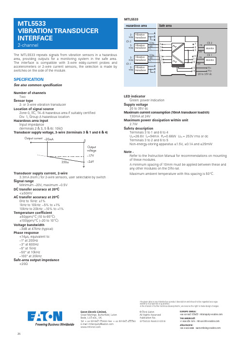
25© 2016 EatonAll Rights Reserved Publication No.Eaton Electric Limited,Great Marlings, Butterfield, Luton Beds, LU2 8DL, UK.Tel: + 44 (0)1582 723633 Fax: + 44 (0)1582 422283E-mail:********************EUROPE (EMEA):+44(0)******************************THE AMERICAS:+********************************ASIA-PACIFIC:+*********************************The given data is only intended as a product description and should not be regarded as a legal warranty of properties or guarantee.In the interest of further technical developments, we reserve the right to make design changes.The MTL5533 repeats signals from vibration sensors in a hazardous area, providing outputs for a monitoring system in the safe area. The interface is compatible with 3-wire eddy-current probes and accelerometers or 2-wire current sensors, the selection is made by switches on the side of the module.SPECIFICATIONSee also common specificationNumber of channelsTwoSensor type2- or 3-wire vibration transducer Location of signal sourceZone 0, IIC, T4–6 hazardous area if suitably certified Div. 1, Group A hazardous location Hazardous-area inputInput impedance(terminals 2 & 3, 5 & 6): 10kΩTransducer supply voltage, 3-wire (terminals 3 & 1 and 6 & 4)Output current –20mAOutput voltage –24V0350Ω–17VTransducer supply current, 2-wire3.3mA (nom.) for 2-wire sensors, user selectable by switch Signal rangeMinimum –20V, maximum –0.5V DC transfer accuracy at 20°C<±50mVAC transfer accuracy at 20°C0Hz to 1kHz: ±1%1kHz to 10kHz: –5% to +1%10kHz to 20kHz: –10% to +1%Temperature coefficient±50ppm/°C (10 to 65°C)±100ppm/°C (–20 to 10°C)Voltage bandwidth–3dB at 47kHz (typical)Phase response<14µs, equivalent to:–1° at 200Hz –3° at 600Hz –5° at 1kHz –50° at 10kHz –100° at 20kHzSafe-area output impedance<20ΩLED indicatorGreen: power indication Supply voltage20 to 35V dcMaximum current consumption (10mA transducer load/ch)130mA at 24VMaximum power dissipation within unit2.7WSafety descriptionTerminals 3 to 1 and 6 to 4U o =26.6V I o =94mA P o =0.66W U m = 253V rms or dc Terminals 3 to 2 and 6 to 5Non-energy-storing apparatus ≤1.5V, ≤0.1A and ≤25mWNote -Refer to the Instruction Manual for recommendations on mounting of these modules.A minimum spacing of 10mm must be applied between these and any other modules on the DIN-rail.Maximum ambient temperature with this spacing is 50°C.MTL5533EPSx533 Rev6 010916。
SPCA-533A中文资料

DIGITAL STILL CAMERA CONTROLLER1. General DescriptionThe SPCA533A is a highly integrated solution for DSC (Digital Still Camera) application. It consists of image processing engine, image compression engine, the storage interface controller, TV encoder, LCD interface controller and USB interface. The SPCA533A supports a wide range of sensors, including most-commonly used CMOS and CCD sensors. Flexible control of the internal buffer allows the SPCA533A chip to support up to 4-mega pixels image resolution. It also supports many flash memory card interfaces, including CFC, MMC, SMC, and SD. The SPCA533A can also interface to both TFT LCD panels and STN LCD panels for preview. With the fully supports to a DSC’s major peripherals, the customers can realize a DSC system with the minimum cost.2. FeaturesDual mode operation, support PC-camera mode and Digital Still camera modeSupport major CMOS sensors and CCD sensorsCMOS sensors:CIF/100K Agilent HDCS1020, Photobit PB100/101, OmniVision OV6620, Hynix HV7121B, Sharp LZ34C10, TASCTAS5110A, Pixart PAS106BVGA/300K Agilent HDCS2020, Photobit PB320, OmniVision OV7620, Hynix HV7131B, Sharp LZ34B10, PIXART PAS102, TASC TAS5130A, Biomorphic BI8602, IC Media ICM205DL, Motorola SCM20014, National SemiconductorLM9627,Century Semiconductor CS2102SVGA/500K PixelCam PCS2112, Hynix HV7141B1.3M OmniVision OV9620, Motorola MCM200273M Y-medai YM3170CCD sensors:VGA/300K Sharp LZ24BP, Sony ICX098AK, Panasonic MN37771ICX204AK800K Sony1.3 M SharpLZ23J3V, Sharp RJ23J3A, Sharp RJ24J3A, Sony ICX202AQ, Panasonic MN397421.45M Sony ICX205AK2.0M Sharp LZ21N3V, RJ23N3A, Sony ICX224AQ, Sony ICX284AQ, Panasonic MN394713.0M Sony ICX262AQ, Sharp RJ21P3A, Panasonic MN395924.0M Sony ICX406AQF,Mechanical shutter and flash light control supportReal timer scaling function in the preview and video clip modeTwo-dimensional edge enhancementExcellent color correction and interpolation25 AE/AWB measurement windows, full image coverageBad-pixel correction up to 256 pixelsBuilt-in TV encoder with DAC, support both NTSC and PAL composite videoDigital TV output interface, conform to CCIR601(8-bit/16-bit data bus) and CCIR656 standardDigital TV input interface, CCIR601(8-bit data bus) and CCIR656Digital TFT LCD output interface, Unipac, Epson, Casio, Prime viewDigital STN LCD panel interface for GiantPlus panelsSupport font-based OSD and graphic-based OSDSupport SDRAM interface, 16M/64M/128M/256MStorage media interface, SD/Nand-gate flash/MMC/CFA/SMCcodecBuilt-inAudiointerface(AC-link)AC-97codecDigitalcompression/decompressionaudioIMAADPCMSerial interface to integrate with Sunplus’s MP3 decoder (SPCA751)Standard JPEG compression/decompression engine.Built-in 8032 micro-controller with 8K bytes SRAM(in-system-programming)functionISPSupportSupport ICE interface to ease system developmentExtended external ROM space, up to 1M bytesPWMoutputsprogrammableFourUSB1.1 interface, support 10 pipes3.3V/2.5V dual power supplyPackageLQFP216/LQFP256/TFBGA2803. Functional Block Diagram and ApplicationsColor DSP: Image processing engine of the SPCA533A is a very flexible pipeline. It will perform color interpolation, gamma correction, image scaling for digital zoom, and image enhancement filtering.JPEG Engine: This image compression engine can generate JPEG compressed file in JFIF and EXIF format with firmware support. The engine can also decode JPEG compressed image for playback.DRAM Controller: The DRAM controller provides access path to the SDRAM for the other internal modules of the SPCA533A. Many special。
A2636 中文数据手册 V0.7

,3
Z2
4
L
5
M
6
R
7
பைடு நூலகம்OPT
8
LED
9
PS2_DATA
10
PS2_CLK
11
AVDD
12
VDD5V
A2636
3D U+P CMOS 光学鼠标单芯片
I/O
描叙
_
电源地
I
Z轴输入1
I
Z轴输入2
I
左键
I
中键
I
右键
I/O
DPI设置脚
O
LED 驱动
I/O
USB D- 或者 PS/2 数据
I/O
USB D+ 或者 PS/2 时钟
版本:0.7
3/10
2008 年 8 月 29 日
A2636
3D U+P CMOS 光学鼠标单芯片
6. 电气参数
标识符
IDD
VIL1 VIH1
VIL2 VIH2
VIL3 VIH3 VPOR IOL1
描叙
工作状态下的消耗电流e
待命状态下的消耗电流 输入输出口低电平 输入输出口高电平
USB输入输出口低电平 USB输入输出口高电平
最小 值
0 4.5
2000 2.3 0
典型 值
5.0
2.4
800
最大值
40 5.5 100 4000 2.5 24 16 1600
单位
摄氏度 伏 毫伏
帧/秒 毫米 英寸/秒
g 点/英寸
注解 800或者1600
___________________________________________________________________________________________
ftc533规格书
ftc533规格书FTC533规格书引言FTC533是一份规格书,旨在详细描述FTC533产品的技术规格和性能特点。
本文将对FTC533的主要特点进行介绍,包括硬件配置、软件功能和性能参数等方面的详细说明。
一、硬件配置1. 处理器:FTC533采用高性能处理器,能够提供强大的计算能力和数据处理能力。
2. 内存:FTC533配置大容量内存,可以支持高性能应用程序的运行。
3. 存储:FTC533提供大容量的存储空间,可以存储大量的数据和文件。
4. 网络接口:FTC533支持多种网络接口,包括以太网接口和无线网络接口,实现与外部设备的连接和数据传输。
5. 外部接口:FTC533提供多个外部接口,包括USB接口、HDMI接口等,方便用户进行外部设备的连接和数据传输。
6. 显示屏:FTC533配备高清显示屏,可以提供清晰、逼真的图像显示效果。
二、软件功能1. 操作系统:FTC533采用先进的操作系统,具有友好的用户界面和丰富的功能,可以满足用户的多样化需求。
2. 应用软件:FTC533预装了多种实用的应用软件,包括办公软件、娱乐软件等,方便用户进行各种操作和应用。
3. 数据安全:FTC533具备完善的数据安全功能,包括数据加密、用户身份认证等,保护用户数据的安全性和隐私。
4. 远程管理:FTC533支持远程管理功能,用户可以通过网络远程管理设备,实现远程监控和操作。
三、性能参数1. 处理性能:FTC533处理器具有高性能和低能耗的特点,可以提供快速响应和高效运行。
2. 网络性能:FTC533网络接口支持高速数据传输,具有稳定和可靠的网络连接能力。
3. 存储性能:FTC533存储器具有高速读写能力,可以实现快速的数据存储和访问。
4. 显示性能:FTC533显示屏具有高清、逼真的图像显示效果,可以提供优质的视觉体验。
5. 电池续航:FTC533配备高容量电池,可以支持长时间的使用,满足用户的移动需求。
结论FTC533是一款配置高、性能优越的设备,具有强大的处理能力、丰富的功能和稳定可靠的性能。
533mcp 参数
533mcp 参数什么是533mcp?533mcp是一种参数,用于描述和控制电子设备的性能和功能。
533mcp代表着五个不同的参数,分别是:5G网络、3GB RAM、3GB存储容量、5000mAh电池容量和13MP相机。
5G网络5G网络是下一代移动通信技术,提供更快的速度、更低的延迟和更大的容量。
它将带来更好的网络体验,支持更多的设备连接和更快的数据传输。
533mcp中的5G网络意味着设备可以在5G网络下进行高速的互联网访问,观看高清视频、玩游戏和下载文件都将更加快速和稳定。
3GB RAMRAM(随机存取存储器)是电子设备中的一种内存,用于临时存储正在运行的程序和数据。
533mcp中的3GB RAM表示设备具有3GB的内存,可以同时运行多个应用程序和任务,提供流畅的用户体验。
较大的RAM容量还可以提高设备的多任务处理能力和性能。
3GB存储容量存储容量是指设备用于存储数据和文件的空间大小。
533mcp中的3GB存储容量意味着设备具有3GB的可用存储空间,可以存储大量的应用程序、照片、视频和文件。
用户可以轻松地保存和访问他们的个人和工作文件,而不必担心空间不足的问题。
5000mAh电池容量电池容量是指电池存储的电荷量,它决定了设备能够提供的使用时间和续航能力。
533mcp中的5000mAh电池容量表示设备具有5000毫安时的电池容量,可以提供较长的使用时间。
用户可以更长时间地使用设备,而不必频繁充电。
高容量的电池还可以支持设备在高负载情况下的稳定运行。
13MP相机相机是设备中的一个重要功能,用于拍摄照片和录制视频。
533mcp中的13MP相机表示设备具有1300万像素的摄像头。
较高的像素数意味着设备可以拍摄更清晰、更详细的照片和视频。
用户可以捕捉到更多的细节,并享受更好的拍摄体验。
总结533mcp参数包括5G网络、3GB RAM、3GB存储容量、5000mAh电池容量和13MP相机。
这些参数提供了一种全面、高性能的电子设备体验。
ip5306英文规格书
ip5306英文规格书The IP5306 is a power management IC commonly used in portable electronic devices. It provides various functionsto efficiently manage the power supply and charging system. Here is a comprehensive overview of the IP5306 specifications:1. Input Voltage Range: The IP5306 supports a wideinput voltage range, typically from 4.5V to 28V. Thisallows it to be used with various power sources such as USB, AC adapters, and batteries.2. Output Voltage Range: The IP5306 provides multiple output voltage channels to power different components ofthe device. The typical output voltage ranges are as follows:VOUT1: 1.8V to 5.5V.VOUT2: 1.8V to 5.5V.VOUT3: 1.8V to 5.5V.VOUT4: 1.8V to 5.5V.VOUT5: 1.8V to 5.5V.3. Charging Functionality: The IP5306 integrates a charging circuitry that supports various charging modes, including linear charging, constant current charging, and constant voltage charging. It also provides protection features such as overvoltage protection, overcurrent protection, and thermal regulation.4. Battery Management: The IP5306 includes a battery management system to monitor the battery status and ensure optimal charging and discharging. It supports various battery types, including lithium-ion, lithium-polymer, and lithium iron phosphate.5. Power Path Management: The IP5306 incorporates power path management functionality, allowing the device tooperate from either the input power source or the battery, depending on the availability and priority settings.6. Efficiency: The IP5306 is designed to provide high efficiency power conversion, reducing power losses and maximizing battery life. It achieves this through features like synchronous rectification and low dropout voltage.7. Protection Features: The IP5306 includes a range of protection mechanisms to safeguard the device and the connected components. These features include overvoltage protection, overcurrent protection, short circuit protection, and thermal shutdown protection.8. Package: The IP5306 is available in various package options, such as QFN, SOP, and TSSOP, providing flexibility for different PCB layouts and assembly processes.9. Additional Features: The IP5306 may also include additional features such as power sequencing, power-on reset, and programmable current limits to further enhance its functionality and adaptability to differentapplications.It's important to note that the above specifications are general and may vary depending on the specific variant or version of the IP5306. For detailed and up-to-date information, it is recommended to refer to the official datasheet or technical documentation provided by the manufacturer.。
APL5336中文资料

Simplified Application Circuit
VCNTL +5V VIN +1.8V/+1.5V
Shutdown Enable
1 VIN
6 VCNTL
APL5336 3 VREF VOUT 4
GND
2
VOUT 0.9V / 0.75V
General Description
The APL5336 linear regulator is designed to provide a regulated voltage with bi-direction output current for DDRSDRAM termination voltage. The APL5336 integrates two power transistors to source or sink load current up to 1.5A. It also features internal soft-start, current-limit, thermal shutdown and enable control functions into a single chip. The internal soft-start controls the rising rate of the output voltage to prevent inrush current during start-up. The current-limit circuit detects the output current and limits the current during short-circuit or current overload conditions. The on-chip thermal shutdown provides thermal protection against any combination of overload that would create excessive junction temperatures. The output voltage of APL5336 is regulated to track the voltage on VREF pin. An proper resistor divider connected to VIN, GND, and VREF pins is used to provide a half voltage of VIN to VREF pin. In addition, connect an external ceramic capacitor and a open-drain transistor to VREF pin for external soft-start and shutdown control. Pulling and holding the voltage on VREF below the enable voltage threshold shuts down the output. The output of APL5336 will be high impedance after being shut down by VREF or the thermal shutdown function.
Eaton Moeller 系列 CI 保险组合封闭型 263526 产品说明书

Eaton 263526Eaton Moeller® series CI Insulated enclosure, IP55_x, rotary handle black grey, for PKZ0 CI-PKZ0-GVMGeneral specificationsEaton Moeller® series CI Insulated enclosure263526126 mm158 mm 80 mm 0.2 kg CECI-PKZ0-GVMProduct NameCatalog Number Product Length/Depth Product Height Product Width Product Weight Compliances Model Code0 AAccessoriesIs the panel builder's responsibility. The specifications for the switchgear must be observed.0 W10 WMeets the product standard's requirements.Is the panel builder's responsibility. The specifications for the switchgear must be observed.Does not apply, since the entire switchgear needs to be evaluated.Meets the product standard's requirements.Black-gray rotary knobPE(N) terminalMeets the product standard's requirements.Meets the product standard's requirements.Is the panel builder's responsibility.Is the panel builder's responsibility.IP55NEMA Other DA-CE-ETN.CI-PKZ0-GVMIL03407019ZDA-CD-ci_pkz0_gvmDA-CS-ci_pkz0_gvmeaton-manual-motor-starters-enclosure-ci-insulated-enclosure-dimensions.epseaton-manual-motor-starters-mounting-ci-insulated-enclosure-dimensions-002.epseaton-manual-motor-starters-enclosure-ci-k-accessory-dimensions-002.epseaton-manual-motor-starters-enclosure-ci-insulated-enclosure-3d-drawing-003.epsRated operational current for specified heat dissipation (In) Product category10.11 Short-circuit ratingEquipment heat dissipation, current-dependent PvidHeat dissipation capacity Pdiss10.4 Clearances and creepage distances10.12 Electromagnetic compatibility10.2.5 Lifting10.2.3.1 Verification of thermal stability of enclosuresFitted with:10.2.3.2 Verification of resistance of insulating materials to normal heat10.2.3.3 Resist. of insul. mat. to abnormal heat/fire by internal elect. effects10.8 Connections for external conductors10.9.2 Power-frequency electric strengthDegree of protection eCAD model Installeringsinstruksjoner mCAD model TegningerAmbient operating temperature - max70 °C10.7 Internal electrical circuits and connectionsIs the panel builder's responsibility.10.10 Temperature riseThe panel builder is responsible for the temperature rise calculation. Eaton will provide heat dissipation data for the devices.Static heat dissipation, non-current-dependent Pvs0 W10.9.3 Impulse withstand voltageIs the panel builder's responsibility.Enclosure materialPlasticKnockouts2 x M25 (cable entry knockout with thread at the top)Hard mirror with cable entry knockouts (can be cut out)2 x M25 (cable entry knockout with thread at the bottom)2 x M20 (cable entry knockouts at the rear)Ambient operating temperature - min-25 °C10.2.2 Corrosion resistanceMeets the product standard's requirements.10.6 Incorporation of switching devices and componentsDoes not apply, since the entire switchgear needs to be evaluated.10.2.4 Resistance to ultra-violet (UV) radiationPlease enquire10.2.7 InscriptionsMeets the product standard's requirements.10.5 Protection against electric shockDoes not apply, since the entire switchgear needs to be evaluated.Used with+ U or A, +L-PKZ0 (2 units), PKZM0-… and VHIModelSurface mounting10.13 Mechanical functionThe device meets the requirements, provided the information inEaton Corporation plc Eaton House30 Pembroke Road Dublin 4, Ireland © 2023 Eaton. Med enerett.Eaton is a registered trademark.All other trademarks are property of their respectiveowners./socialmediathe instruction leaflet (IL) is observed.Does not apply, since the entire switchgear needs to be evaluated.Is the panel builder's responsibility.Does not apply, since the entire switchgear needs to be evaluated.0 W10.2.6 Mechanical impact10.9.4 Testing of enclosures made of insulating material 10.3 Degree of protection of assembliesHeat dissipation per pole, current-dependent Pvid。
add533 手册
add533 手册【实用版】目录1.引言2.add533 手册的内容概述3.手册的主要章节和重点内容4.如何使用和理解手册5.结论正文1.引言add533 手册是一本非常实用的指南,它涵盖了许多关于 add533 设备的信息和操作方法。
无论是对于初学者还是有经验的用户,这本手册都是非常有价值的参考资料。
在这篇文章中,我们将详细介绍这本手册的内容和如何有效地使用它。
2.add533 手册的内容概述add533 手册主要包括以下几个方面的内容:设备概述、设备安装和配置、操作方法和技巧、故障排除和维护、以及安全注意事项等。
这本手册的目标是帮助用户更好地理解 add533 设备的工作原理,并提供操作指导,以便用户能够更加高效地使用这个设备。
3.手册的主要章节和重点内容在 add533 手册中,以下几个章节是重点内容:- 设备概述:这个章节介绍了 add533 设备的基本信息,包括设备的主要功能、适用场景和使用限制等。
- 设备安装和配置:这个章节提供了详细的安装和配置步骤,包括设备的硬件安装和软件配置等。
- 操作方法和技巧:这个章节主要介绍了如何有效地使用 add533 设备,包括基本操作和进阶技巧等。
- 故障排除和维护:这个章节提供了一些常见的故障排除方法和设备的维护建议,以保证设备的长期稳定运行。
- 安全注意事项:这个章节强调了使用 add533 设备时需要注意的安全问题,以避免可能的安全风险。
4.如何使用和理解手册在使用 add533 手册时,以下几个建议可以帮助你更好地理解和使用手册:- 首先,仔细阅读手册的目录,了解手册的主要内容和结构,以便快速找到你需要的信息。
- 其次,阅读设备概述章节,以便对 add533 设备有一个基本的了解。
- 然后,根据你的需要,选择性地阅读其他章节,以获取更多的操作技巧和故障排除方法。
- 最后,将手册作为参考资料,随时查阅,以便在操作过程中解决可能出现的问题。
5.结论总的来说,add533 手册是一本非常实用的参考资料,它提供了关于add533 设备的全面信息和操作指导。
矽力杰-时钟芯片Si5338 56使用手册-I2C配置说明书

Configuring the Si5338/56 via I2CNVM vs. I2C Configuration differences:First, a note on what can and can’t be done via I2C to clear up any confusion. You can configure theSi5338/56 in-system via I2C, but you can NOT program the device’s OTP NVM in-system. Programming the NVM of blank devices for prototyping purposes can be done using our Si5338/56-PROG-EVB field programmer board, but this is not practical or recommended for production quantities. For production quantities, once you have a working configuration, you can order custom devices from our factory pre-programmed with your specific configuration. There is no additional charge for factory programming and lead times are relativ ely short. To create a custom device use the “Create Custom Device” selection in Clock Builder Desktop. Creating a custom device will generate a unique orderable part number (OPN) for your specific part. See the Si5338 (or Si5356) data sheet, section 3.5 and 3.5.1 for more information.General I2C configuration information:Focusing specifically on in-system I2C device configuration, you can use any I2C bus master that allows both read and write cycles over the I2C bus (e.g. MCU or FPGA). The basic Si5338/56 I2C configuration process requires reading registers (sometimes referred to as RAM in data sheet), modifying the data programmatically, and then writing a new value. As long as the I2C bus master adapter can do these operations, you should be able to configure the device. I2C configuration can be done to any Si5338/56 device variant with I2C bus support, whether it is a custom part or blank part.Creating a configuration to load into registers (RAM) is different than creating a NVM configuration. Please refer to the Si5338 data sheet, sections 3.5.2 and 3.5.3 (or Si5356 data sheet section 3.5). For hardware design related data specific of our I2C interface, please refer to Si5338 data sheet Table 15 “I2C specifications (SCL, SDA)”. (For Si5356 data sheet refer to Table 6.)We provide the details of the I2C configuration process and sample C code (in application note AN428 detailed below). We don’t provide any software drivers or HDL code (for FPGAs). Please read the following documents on next page for more details when crafting your specific I2C configuration strategy.How to configure Si5338/56 via I2C:There are 3 main documents to use as a reference in understanding the I2C configuration process. If you are new to the I2C configuration process, please review these closely. You must follow the complete process described in the documents listed below in order for the device to work properly. The documents below can be used for both Si5338 and Si5356.1) Si5338 data sheet:https:///Support%20Documents/TechnicalDocs/Si5338.pdfRead sections 3.5.1, 3.5.2, and 3.5.3 as well as Figure 9. (Section 3.5.4 describes the Field Programmer for NVM programming of prototype parts.) These sections of the data sheet outlines the process that must be followed when loading a new configuration. Note: The entire register map must be written when making configuration changes. Do not change individual registers based on looking at file differences when changing/modifying configurations, this can lead to improper configuration of the device.2) AN428:https:///Support%20Documents/TechnicalDocs/AN428.pdfAN428 is an application note that describes in-system configuration via I2C using a microcontroller (MCU). It contains C source code for our C8051F3xx MCU family. The code specific to performing theSi5338 configuration starts on page 24 of this document and it implements the flow chart shown in Figure 9 of the Si5338 data sheet. (This code can be used as a guide to implement your own code.) The data array required for this code, which contains the register settings plus the write-allowed mask, can be automatically generated using Clock Builder Desktop. (See Si5338 data sheet, section 3.5.2, item1.g.).Importantly, please closely adhere to, and do not deviate from, not only the event sequences as indicated in the Figure 9 flowchart, but the required time delays as well. You must use the “write-allowed” masks when writing to registers because some registers contain bits that should not be modified and can’t be determined beforehand. Doing the required read/modify/write register operation is essential.3) Si5338 Reference Manual:https:///Support%20Documents/TechnicalDocs/Si5338-RM.pdfThis is a good reference document to understand how the device works with detailed register descriptions. It contains a good "from scratch" description of how to configure the device without using Clock Builder Desktop, but...we strongly recommend leveraging Clock Builder Desktop and the C code in AN428 if possible.。
ap6256模块规格书
AP6256模块规格书包含以下内容:
AP6256是一款高速、高分辨率的图像传感器模块,采用4通道模拟数字转换器,实现了对高动态范围和自动曝光/自动白平衡图像的高精度处理。
以下是模块规格书的一些关键信息:
1. 工作电压范围:模块工作电压为
2.7V~5V,内置备份电源(用于省电),以及两个32位计数器,可以支持不同的应用方案。
2. 高速图像处理能力:该模块具备高速图像处理能力,采用无重影电子快门,最快输出速度可达60fps。
此外,该模块支持图像与视频同步输出,最高支持LVDS 6通道输出。
3. 高分辨率和自动曝光/白平衡:AP6256具有12位的高分辨率和高达300万像素/秒的图像输出速度,并具备自动曝光/白平衡功能。
该模块适用于安全驾驶、机器人视觉、工业控制、无人机、网络摄像机等应用领域。
4. 集成度和灵活性:该模块具有高度集成和定制的灵活性,可直接替换型号为MT9P9813的图像传感器。
它还支持通过I2C接口进行编程和配置,以满足不同应用场景的需求。
此外,AP6256模块还具有低功耗、低噪声、高灵敏度等特点,适用于需要高速图像采集和处理的场景。
需要注意的是,以上信息仅为AP6256模块的部分规格,完整的使用说明和操作指南应该参考制造商提供的官方规格书。
在使用该模块时,请务必遵守相关规范和安全指南,以确保操作安全和稳定性。
CR5335和CR5336和CR5337中文版技术说明书
原边控制高 原边控制高精度恒流/恒压 PWM 功率开关
主要特点
恒压和恒流控制,精度可达±5% ±1%的内部基准电压源 内置高压 MOSFET 原边控制模式,无需 TL431 和光耦 非连续模式下的反激拓扑 具有软启动功能 频率抖动 恒流和输出功率可调 内置次级电压采样控制器 可调式线损补偿 欠压锁定 逐周期电流限制 峰值电流限制 过温保护 过压保护和电源箝位 内置前沿消隐 亚微米高压BiCMOS工艺 DIP-8L、SOP-8L绿色封装
启达科技(成都)有限公司
V1.3 5/10 图2 输出功率随 Rs 的变化曲线
恒压工作
在恒压控制时, CR533X 利用辅助绕组通 过电阻分压器从 INV 采样输出电压,并将采 样的输出电压与芯片内部的基准电压通过误 差放大器进行比较放大,从而调整输出电压。 当采样电压高于内部基准电压, 误差放大器的 输出电压 COMP 减小, 从而减小开关占空比; 当采样电压低于内部基准电压时, 误差放大器
* 集成化功率 MOSFET 的内阻和封装形式、散热、环境温度都有关系,本说明书所给值为室温 下分立封装的 MOSFET 内阻。
启达科技(成都)有限公司
V1.3 4/10
成都启臣微电子有限公司
CR533X
原边控制高 原边控制高精度恒流/恒压 PWM 功率开关
工作描述 启动电流和启动控制
应用
AC/DC电源适配器 DVD/DVB电源 充电器 ADSL等无线路由器开关电源 LED照明电源
概述
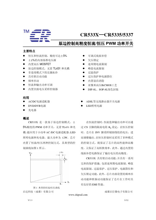
CR533X 是一款基于原边控制模式、± 5%精度的 PWM 功率开关,无需 TL431 和光 LED 耦, 能应用于小功率 AC /DC 电源适配器、 照明电源和充电器,最大功率为 12W。芯片 内置了恒流/恒压两种控制方式,其典型的控 制曲线如图 1 所示。 在恒流控制时, 恒流值和输出功率可以通 过 CS 引脚的限流电阻 RS 设定;在恒压控制 时,芯片在 INV 脚采样辅助绕组的电压,进 而调整输出。 在恒压控制时还采用了多种模式 的控制方式,既保证了芯片的高性能和高精 度,又保证了高转换效率。此外,通过内置的 线损补偿电路保证了输出电压的高精度。 CR533X 具有软启动功能, 并具有一系列 完善的保护措施, 包括逐周期电流限制、 峰值 电流限制、过温保护、过压保护、电源箝位和 欠压锁定功能。 此外, 芯片内部设置的频率抖 动功能和软驱动功能保证了芯片在工作时具 有良好的 EMI 性能。
海利普变频器说明书C100

围。
HLP-C100 系列使用说明书
系列
危险
● 变频器运转中严禁将电机机组投入或切离,否则会造成变频器 过电流跳脱,甚至烧毁变频器主回路。
72
10.1 故障列表
72
10.2 操作异常及处理
73
第11章 日常维护
75
11.1 注意事项
75
11.2 变频器存储和运输
75
第12章 通讯协议
76
12.1 格式说明
76
12.2 线圈寄存器编址
76
12.3 读线圈状态
78
12.4 读保持寄存器
79
12.5 写单个线圈状态
79
12.6 写单个保持寄存器值 12.7 写多个线圈状态 12.8 写多个保持寄存器 12.9 读写数组参数 12.10 通信错误代码
系列
1 1 2 2 3 4 4 5 5 8 8 8 8 9 9 9 9 11 13 14 14 14 15 16 18 19 20 21 21 21 21
系列
5.4 正反转、点动
21
5.5 多段速
22
5.6 故障复位
23
第6章 功能参数表
24
第7章 参数详细说明
34
7.1 第00组参数:操作/显示
34
7.2 第01组参数:负载/电动机
36
7.3 第02组参数:制动功能
40
7.4 第03组参数:设定值/加减速
41
7.5 第04组参数:极限/警告设置
沃普萨 HUMICAP HMT330 配 Заpared 湿度传感器和温度传感器系列说明书
The HMT330 transmitter family has the solution for demanding industrial humidity measurements.HMT330 Series Humidity and Temperature Transmitters for Industrial ApplicationsThe Vaisala HUMICAP® Humidity and Temperature Transmitter Series HMT330 is designed for demanding industrial applications where stable measurement and wide customization possibilities are important.Vaisala HUMICAP ®performanceThe HMT330 series incorporates Vaisala’s 30 years of experience in industrial humidity measurement. The sensor measures accurately andreliably and is immune to particulate contamination and most chemicals.Chemical purge minimizes effects of contaminantsIn environments with highconcentrations of chemicals andcleaning agents, chemical purge helps to maintain the accuracy between calibration intervals.Chemical purge involves heating the sensor to remove harmful chemicals.The function can be initiated manually or programmed to occur at set intervals.Graphical measurement trend and history displayThe HMT330 can be ordered with a large numerical and graphical display,allowing the user to easily monitor measurement trends and 1-year history.Data collection and transfer to PCThe recorded measurement data can be viewed on the display or transferred to PC with Windows®-based software .Many ways to installMains and DC power options, and several mounting accessories make it easy to install the instrument.Versatile outputsThe HMT330 can have up to three analog outputs. Galvanic isolation of supply power and analog outputs is also available. For digitalcommunication, the RS-232, RS-485 or relay outputs can be used.Flexible calibrationThe HMT330 instruments are factory-calibrated at six humidity points.A quick one-point field calibration can be performed with the hand-held HM70 meter.A two-point calibration can beperformed with the HMK15 salt bath calibrator in a controlled environment.The transmitter can be sent to Vaisala for recalibration. Accredited calibrations and maintenance contracts are also available.The display shows measurement trends and history up to 1 year.HUMICAP® is a registered trademark of Vaisala.Specifications subject to change without prior notice.©Vaisala OyjPerformanceRelative humidity Measurement range 0...100 %RH Accuracy against factory standards including non-linearity,hysteresis and repeatabilityat +20 °C (+68 °F)± 1 %RH (0...90 %RH)± 1.7 %RH (90...100 %RH)at -20...+40 °C (-4...+104 °F)± (1.0 + 0.008 x reading) %RH*at -40...-20 °C, +40...+180 °C (-40...-4 °F, +104...+356 °F)± (1.5 + 0.015 x reading) %RH*Factory calibration uncertainty** (+20 °C / +68 °F)0...40 %RH ± 0.6 %RH 40...97 %RH ± 1.0 %RH Humidity sensorsfor typical applications Vaisala HUMICAP® 180chemical purge/warmed probe Vaisala HUMICAP® 180C high chemical concentrations*Vaisala HUMICAP® 180L2** For Vaisala HUMICAP® 180L2 sensorat -10...+40°C (+14...+104 °F)± (1.0 + 0.01 x reading) %RH at -40...-10 °C,+40...+180 °C (-40...+14 °F, +104...+356 °F)± (1.5 + 0.02 x reading) %RH** Defined as ±2 standard deviation limits.Response time (90 %) at 20 °C (+68 °F) in still air with grid filter 8 s with grid + steel netting filter 20 s with sintered filter 40 s TemperatureMeasurement range HMT331-40...+60 °C HMT333-40...+80 °C HMT334, HMT335, HMT337, HMT338-70...+180 °C Accuracy at +20 °C (+68 °F)± 0.2 °C Accuracy over temperature rangeTemperature sensor Pt 100 RTD 1/3 Class B IEC 751Other variables Other variables available (depends on model)dewpoint temperature, mixing ratio, absolute humidity, wet bulb temperature, enthalpy, water vapor pressureOperating environmentOperating temperature for probesame as measurement rangesfor transmitter body -40...+60 °C (-40...+140 °F)with display 0...+60 °C (+32...+140 °F)Operating pressure HMT3340...10 MPa (0...100 bar)HMT3380...4 MPa (0...40 bar)HMT333, HMT335, HMT337vapor tightComplies with EMC standard EN61326-1:1997 + Am1:1998 +Am2:2001; Industrial Environment.Inputs and outputsOperating voltage 10...35 VDC, 24 VAC with optional power supply module 100...240 VAC 50/60 Hz Power consumption @ 20 °C (U in 24VDC)RS-232max 25 mAU out 2 x 0...1V / 0...5V / 0 (10V)max 25 mA I out 2 x 0...20 mAmax 60 mA display and backlight + 20 mA during chemical purge + 110 mA max during probe heating (HMT337)+ 120 mA Analog outputs (2 standard, 3rd optional)current output 0...20 mA, 4...20 mA voltage output 0...1 V, 0...5 V, 0...10 V Accuracy of analog outputs at 20 °C ± 0.05 % full scale Temperature dependence of analog outputs ± 0.005 %/°C of full scale External loads current ouputs R L < 500 ohm 0... 1 V output R L > 2 kohm 0... 5 V and 0... 10 V outputs R L > 10 kohm Max wire size 0.5 mm 2 (AWG 20),stranded wires recommendedDigital outputs RS-232, RS-485 (optional)Relay outputs (optional)0.5 A, 250 VAC Display LCD with backlight, graphictrend display of any parameterMenu languages English, French, Spanish,German, Japanese, Swedish, FinnishMechanicsCable bushing M20x1.5 (cable diameter 8...11mm)Conduit fitting M20x1.5 / 1/2"NPT 8-pole connector (male)RKC8/9.M128-pole connector with 5 m cable (female)RKT8-282/5M Probe cable diameter HMT333 6.0 mm other probes 5.5 mm Housing material G-AlSi 10 Mg (DIN 1725)Housing classification IP 65 (NEMA 4)Dimensionsdimensions in mm (inches)HMT331 Humidity and Temperature Transmitter for Demanding Wall-Mount ApplicationsThe Vaisala HUMICAP® Humidity and Temperature Transmitter HMT331 is the top-of-the-line wall-mounttransmitter for demanding HVAC and condition monitoring pared to regular wall-mount transmitters, the HMT331 offers:-Higher measurement performance -Better chemical tolerance-Advanced graphical display features -More powering options -More output options-A wider variety of output humidity parameters.Graphical measurement trend and history displayThe HMT330 series features a large numerical and graphical display,allowing the user to easily monitor measurement trends and 1-year history.The measurement history is especially useful in stability rooms and archives.The minimum and maximum values for the previous year can be viewed.Outputs and power supply options for every needThe output options include three analog outputs, RS-232, RS-485, and alarm relays.The voltage supply range is from 10 to 35 VDC. With an additional module,the transmitter can be connected to all universal mains AC supplies.The input/output cable can be fed through the back of the transmitter,which is a useful installation feature especially in cleanrooms.Technical DataTemperature measurement range-40...+60 °C (-40...+140 °F)AccessoriesPC software + cable215005Connection cable for HM70211339Wall mounting plate (plastic)214829Pole installation kit 215108Rain shield215109DIN rail installation set211477DimensionsDimensions in mm (inches)The HMT331 is the state-of-the-art wall-mount humidity instrument.The display shows measurement trends and 1-year history.HMT333 Humidity and Temperature Transmitter for Ducts and Tight SpacesTechnical DataTemperature measurement range-40...+80 °C (-40...+176 °F)AccessoriesDuct installation kit 210697Cable gland HMP247CG PC software + cable 215005Connection cable for HM70211339Wall mounting plate (plastic)214829Pole installation kit 215108Rain shield 215109Solar radiation shield DTR502B DIN rail installation set 211477DimensionsDimensions in mm (inches)The Vaisala HUMICAP® Humidity and Temperature Transmitter HMT333 is a versatile instrument for applications where a small remote probe is needed.Flexible installationpossibilitiesFor installing the probe in ducts,channels, and through walls, an installation kit consisting of analuminum flange, lead-through piece and steel support bar is available.The probe cable is flexible and available in 2, 5 and 10-meter lengths.In outdoor environments, the DTR502B solar radiation shieldprovides protection for the probe. The shield can be installed on a pole, beam or flat surface.For moderate humidities and temperaturesThe HMT333 is typically used indemanding HVAC applications such as cleanrooms, pharmaceutical processes and greenhouses.For environments with continous high humidity, the HMT337 with a warmed,vapor-tight, stainless steel probe isrecommended instead of the HMT333.The HMT333 transmitter has a small probe for remote applications.Duct installation kit.HMT334 Humidity and Temperature Transmitter for High Pressure and Vacuum ApplicationsTechnical DataTemperature measurement range-70...+180 °C (-94...+356 °F)Operating pressure0...10 MPa (0...100 bar)AccessoriesFitting body ISO M22 x 1.517223Fitting body NPT 1/2”17225PC software + cable215005Connection cable for HM70211339Wall mounting plate (plastic)214829Pole installation kit 215108Rain shield215109DIN rail installation set211477DimensionsDimensions in mm (inches)The Vaisala HUMICAP® Humidity and Temperature Transmitter HMT334 is designed to measure humidity in pressurized spaces or vacuum chambers. Each probe is tested to ensure a gas and vacuum tight installation.Vaisala HUMICAP ®performanceThe HMT334 incorporates Vaisala’s 30years of experience in industrial humidity measurement. The sensor provides accurate and reliable measurement and is immune to particulate contamination and most chemicals.Graphical measurement trend and history displayThe HMT330 series features anumerical and graphical display. The user can easily monitor measurement trends and history with minimum and maximum values for up to 1 year.The HMT334 is ideal for permanent installations into pressurized or vacuum processes.The display shows minimum and maximum values for up to 1 year.Using the serial line the measurement data can be transferred to a PC, where it can be further processed and copied to other programs.HMT335 Humidity and Temperature Transmitterfor High TemperaturesTechnical DataTemperature measurement range-70...+180 °C (-94...+356 °F)AccessoriesMounting flange 210696PC software + cable215005Connection cable for HM70211339Wall mounting plate (plastic)214829Pole installation kit 215108Rain shield215109DIN rail installation set211477DimensionsDimensions in mm (inches)The Vaisala HUMICAP® Humidity and Temperature Transmitter HMT335 has a long stainless steel probe designed for high temperatures.Robust probe ideal for high flow ratesThe probe tolerates mechanical stress and high flow rates. This makes the HMT335 ideal for duct-typemeasurements where smaller probes are not sturdy enough. An example application is a hot drying process.Graphical measurement trend and history displayThe HMT335 features a numerical and graphical display. The user can easily monitor measurement trends and history with minimum and maximum values for up to 1 year.Vaisala HUMICAP ®performanceThe sensor provides accurate and reliable measurement and is immune to particulate contamination and most chemicals.The installation flange allows an adjustableinstallation depth for the probeThe HMT335 has a robust stainless steel probe ideal for high flow rates in hot processes.HMT337 Humidity and Temperature Transmitter for High Humidity ApplicationsThe Vaisala HUMICAP® Humidity and Temperature Transmitter HMT337 is delivered in three configurations:•Basic: non-warmed probe for moderate humidities•With warmed probe: for near-condensing conditions, dewpoint measurement•With warmed probe and additional temperature sensor: for near-condensing conditions, relative humidity measurementTrue humidity readings incondensing conditionsVaisala’s unique warmed probe head provides fast and reliable measurement in environments where humidity is near saturation. The heating helps the sensor to recover very fast from condensation.As the probe head is warmed, the humidity level inside the head stays below the ambient level. With accurate temperature measurement, the ambient dewpoint can be calculated precisely.Technical DataTemperature measurement range-70...+180 °C (-94...+356 °F)AccessoriesCable gland AGRO HMP247CG Duct installation kit (RH-probe)210710Duct installation kit (T-probe)215003Swagelok fittings (NPT and ISO) for both RH and T probes Solar radiation shield DTR502B Meteorological inst. kit HMT330MIK PC software + cable 215005Connection cable for HM70211339Wall mounting plate (plastic)214829Pole installation kit 215108Rain shield 215109DIN rail installation set 211477DimensionsDimensions in If the relative humidity value is needed,an additional temperature sensor head is used. The measured ambient temperature provides thecompensation for calculating the relative humidity and other humidity parameters.Many ways to installDuct installation kit.The HMT337 is the transmitter for the most demanding process and meteorological measurements.HMT338 Humidity and Temperature Transmitter for Pressurized PipelinesTechnical DataTemperature measurement range-70...+180 °C (-94...+356 °F)Operating pressure 0...4 MPa (0...40 bar)AccessoriesBall valve set DMP248BVS PC software + cable 215005Connection cable for HM70211339Wall mounting plate (plastic)214829Pole installation kit 215108Rain shield 215109DIN rail installation set 211477DimensionsDimensions in mm (inches)The Vaisala HUMICAP® Humidity and Temperature Transmitter HMT338 is designed for pressurized processes.Insert or remove probe while the process is runningWith “hot tapping”, the probe isinserted directly into the process while it is running, without exposing the need for venting or lowering the process pressure.The probe head is screwed into a ball valve assembly that has been fixed to the process pipe or wall. The adjustable hex nut is hand-tightened totemporarily hold the probe in the ‘up’position. Then the ball valve is opened,exposing the probe to the process, and the probe is pushed to the proper depth in the ‘down’ position. The hex nut is tightened with a wrench to lock the probe in place. Hot tapping is possible in pressures up to 10 bar.Graphical measurement trend and history displayFrom the display, the user can easily monitor measurement stabilization and process trends. Measurement history with minimum and maximum values is available for up to 1 year.Vaisala HUMICAP ®The HMT338 incorporates Vaisala’s 30years of experience in industrial humidity measurement. The sensor provides accurate and reliable measurement and is immune to particulate contamination and mostchemicals.The HMT338 is ideal for installations in pressurized processes where the probe needs to beremoved while the process is running.。
AQ533资料

Operating Tj %Tol
PKG Type
AQ533
0C˚ ≤ 125C˚
1.0
SOT-23-5
AQ533
0C˚ ≤ 125C˚
1.0
SOT-23-5
AQ533
0C˚ ≤ 125C˚
1.0
SOT-23-5
AQ533
0C˚ ≤ 125C˚
1.0
SOT-23-5
AQ533
0C˚ ≤ 125C˚
1.0
Features • Low dropout voltage (350mV at 500 mA) • Enable pin implements sequencing • Reverse current protection • Vout tolerance less than 1.5% over
temperature
Applications
• Graphic cards • PC motherboards • Cell Phones • DVD video player
The enable pin provides a remote turn-off for low power consumption. It draws virtually zero current in shutdown mode and implements Sequential, Ratiometric, or Simultaneous sequencing schemes. This also allows for a separate bias connection from the pass transistor in order to achieve ultra low dropout from VIN to VOUT.
- 1、下载文档前请自行甄别文档内容的完整性,平台不提供额外的编辑、内容补充、找答案等附加服务。
- 2、"仅部分预览"的文档,不可在线预览部分如存在完整性等问题,可反馈申请退款(可完整预览的文档不适用该条件!)。
- 3、如文档侵犯您的权益,请联系客服反馈,我们会尽快为您处理(人工客服工作时间:9:00-18:30)。
Copyright © ANPEC Electronics 1ANPEC reserves the right to make changes to improve reliability or manufacturability without notice, and advise customers to obtain the latest version of relevant information to verify before placing orders.•Provide Bi-direction Output Currents-Sourcing and Sinking Current up to 1.5A•Built-in Soft-Start•Power-On-Reset Monitoring on VCNTL and VIN pins•Fast Transient Response•Stable with Ceramic Output Capacitors•±20mV High System Output Accuracy over Load and Temperature Ranges•Adjustable Output Voltage by External Resistors •Current-Limit Protection •On-Chip Thermal Shutdown•Shutdown for Standby or Suspend Mode •Simple SOP-8 and SOP-8 with Exposed Pad (SOP-8P) Packages •Lead Free and Green Devices Available(RoHS Compliant)The APL5336 linear regulator is designed to provide a regulated voltage with bi-direction output current for DDR-SDRAM termination voltage. The APL5336 integrates two power transistors to source or sink load current up to 1.5A. It also features internal soft-start, current-limit, ther-mal shutdown and enable control functions into a single chip.The internal soft-start controls the rising rate of the output voltage to prevent inrush current during start-up. The current-limit circuit detects the output current and limits the current during short-circuit or current overload conditions. The on-chip thermal shutdown provides ther-mal protection against any combination of overload that would create excessive junction temperatures.The output voltage of APL5336 is regulated to track the voltage on VREF pin. An proper resistor divider connected to VIN, GND, and VREF pins is used to provide a half voltage of VIN to VREF pin. In addition, connect an exter-nal ceramic capacitor and a open-drain transistor to VREF pin for external soft-start and shutdown control.Pulling and holding the voltage on VREF below the en-able voltage threshold shuts down the output. The output of APL5336 will be high impedance after being shut down by VREF or the thermal shutdown function.FeaturesGeneral DescriptionApplications•DDRII/III SDRAM Termination Voltage •Motherboard and VGA Card Power Supplies •Setop Box•SSTL-2/3 Termination VoltagePin ConfigurationSimplified Application CircuitOUTGND 27 VCNTL VREF 3VOUT 46 VCNTL 5 VCNTL8 VCNTL VIN 1Top View of SOP-8GND 27 NC VREF 3VOUT 46 VCNTL 5 NC8 NC VIN 1Exposed Pad (connected to GND plane for better heat dissipation)Copyright © ANPEC Electronics 2Ordering and Marking InformationAbsolute Maximum Ratings (Note 1)Note 1: Stresses above those listed in “Absolute Maximum Ratings” may cause permanent damage to the device.Thermal CharacteristicsRecommended Operating ConditionsNote 2: θJA is measured with the component mounted on a high effective thermal conductivity test board in free air.Note 3: The exposed pad of SOP-8P is soldered directly on the PCB. The case temperature is measured at the center of the exposed pad on the undersideof the SOP-8P package.APL5336Package CodeK : SOP-8 KA : SOP-8POperating Ambient Temperature RangeI : -40 to 85 CHandling CodeTR : Tape & Reel Assembly MaterialL : Lead Free Device G : Halogen and Lead Free Device°Handling Code Temperature Range Package CodeAPL5336 K:APL5336 XXXXXXXXXX - Date CodeAssembly Material APL5336 KA:APL5336 XXXXXNote: ANPEC lead-free products contain molding compounds/die attach materials and 100% matte tin plate termination finish; which are fully compliant with RoHS. ANPEC lead-free products meet or exceed the lead-free requirements of IPC/JEDEC J -STD-020C for MSL classification at lead-free peak reflow temperature. ANPEC defines “Green” to mean lead-free (RoHS compliant) and halogen free (Br or Cl does not exceed 900ppm by weight in homogeneous material and total of Br and Cl does not exceed 1500ppm by weight).Copyright © ANPEC Electronics 3Electrical CharacteristicsRefer to the typical application circuit. These specifications apply over V CNTL =5V, V IN =1.8V or 1.5V, V REF =0.5V IN , C IN =10µF, C OUT =10µF (MLCC) and T A = -40~85°C, unless otherwise specified. Typical values are at T A =25°C.Recommended Operating Conditions (Cont.)Note 4: The symbol “+” means the VOUT sources current to load; the symbol “-” means the VOUT sinks current from load to GND.Note 5: It’s necessary to use a multi-layer ceramic capacitor 8µF at least as an output capacitor. Please place the ceramic capacitor near VOUT pinas close as possible. Besides, the other kinds of capacitors (like Electrolytic, PoSCap, tantalum capacitors) can be used as the output capacitors in parallel.Copyright © ANPEC Electronics 4Electrical Characteristics (Cont.)Refer to the typical application circuit. These specifications apply over V CNTL =5V, V IN =1.8V or 1.5V, V REF =0.5V IN , C IN =10µF, C OUT =10µF (MLCC) and T A = -40~85°C, unless otherwise specified. Typical values are at T A =25°C.Copyright © ANPEC Electronics 5Typical Operating CharacteristicsVCNTL Power SupplyV C N T L P S R R (d B )Frequency (HZ)01000100001000001000000-4-20246810-50-250255075100125150Junction Temperature (T J ,o C)V O U T O f f s e t V o l t a g e ,V O S (m V )VOUT Offset Voltage vs.Junction TemperatureC Sourcing Current-Limit vs.C u r r e n t -L i m i t ,I (A )0.511.522.53-50-25255075100125Sinking Current-Limit vs.Junction TemperatureJunction Temperature ()o C C u r r e n t -L i m i t ,I L I M (A )0.511.522.533.5-50-25255075100125Sourcing Current-Limit vs.Junction TemperatureC u r r e n t -L i m i t ,I L I M (A )Junction Temperature (T J ,o C)00.511.522.533.54-50-25255075100125Sinking Current-Limit vs.Junction TemperatureC u r r e n t -L i m i t ,I L I M (A )Junction Temperature (T J ,o C)Copyright © ANPEC Electronics 6Operating WaveformsV CNTL = 5V, V IN = 1.8V or 1.5V, V REF =0.5xV IN , C IN =C OUT =10µF(MLCC)CH1: V OUT , 20mV/Div, AC CH2: I OUT , 0.5A/Div, DC TIME: 200µs/DivLoad Transient Response (V IN =1.8V)I OUTV OUTI OUT =10mA to 1.5A to 10mACH1: V OUT , 20mV/Div, AC CH2: I OUT , 0.5A/Div, DC TIME: 1µs/DivV OUTI OUTI OUT =10mA to 1.5ALoad Transient Response (V IN =1.8V)CH1: V OUT , 20mV/Div, AC CH2: I OUT , 0.5A/Div, DCI OUTV OUTI OUT =1.5A to 10mALoad Transient Response (V IN =1.8V)V OUTI OUTCH1: V OUT , 20mV/Div, AC CH2: I OUT , 0.5A/Div, DC TIME: 200µs/DivLoad Transient Response (V IN =1.8V)I OUT =-10mA to -1.5A to -10mACopyright © ANPEC Electronics 7Operating Waveforms (Cont.)V OUTI OUTCH1: V OUT , 20mV/Div, AC CH2: I OUT , 0.5A/Div, DC TIME: 1µs/DivI OUT =-10mA to -1.5ALoad Transient Response (V IN =1.8V)V OUTI OUT CH1: V OUT , 20mV/Div, AC CH2: I OUT , 0.5A/Div, DC TIME: 200µs/Div Load Transient Response (V IN =1.5V)I OUT =10mA to 1A to 10mAV OUTI OUTCH1: V OUT , 20mV/Div, AC CH2: I OUT , 0.5A/Div, DC TIME: 1µs/DivI OUT =10mA to 1ALoad Transient Response (V IN =1.5V)I OUTV OUTCH1: V OUT , 20mV/Div, AC CH2: I OUT , 0.5A/Div, DC TIME: 1µs/DivI OUT =-1.5A to -10mALoad Transient Response (V IN =1.8V)V CNTL = 5V, V IN = 1.8V or 1.5V, V REF =0.5xV IN , C IN =C OUT =10µF(MLCC)Copyright © ANPEC Electronics 8Operating Waveforms (Cont.)I OUTV OUTOUT CH2: I OUT , 0.5A/Div, DC TIME: 1µs/Div I OUT =1A to 10mALoad Transient Response (V IN =1.5V)V OUTI OUTOUT CH2: I OUT , 0.5A/Div, DC TIME: 200µs/DivLoad Transient Response (V IN =1.5V)I OUT =-10mA to -1A to -10mAV OUTI OUTOUT CH2: I OUT , 0.5A/Div, DC TIME: 1µs/Div I OUT =-10mA to -1ALoad Transient Response (V IN =1.5V)OUT CH2: I OUT , 0.5A/Div, DC TIME: 1µs/DivI OUT =-1A to -10mALoad Transient Response (V IN =1.5V)V OUTI OUTV CNTL = 5V, V IN = 1.8V or 1.5V, V REF =0.5xV IN , C IN =C OUT =10µF(MLCC)Copyright © ANPEC Electronics 9Operating Waveforms (Cont.)Power ON Test (V IN =1.5V)CH2: V OUT , 500mV/Div, DC CH3: I OUT , 1A/Div, DC TIME: 50ms/DivCH1: V IN , 1V/Div, DCV INV OUTI OUTR Load =1 ΩPower OFF Test (V IN =1.5V)CH2: V OUT , 500mV/Div, DC CH3: I OUT , 1A/Div, DC TIME: 5ms/DivCH1: V IN , 1V/Div, DCI OUTV OUTV INR Load =1 ΩPower ON Test (V IN =1.8V)CH2: V OUT , 500mV/Div, DC CH3: I OUT , 1A/Div, DC TIME: 50ms/DivCH1: V IN , 1V/Div, DCV INV OUTI OUTR Load =1 ΩPower OFF Test (V IN =1.8V)V INV OUTI OUTR Load =1 ΩCH2: V OUT , 500mV/Div, DC CH3: I OUT , 1A/Div, DC TIME: 5ms/DivCH1: V IN , 1V/Div, DCV CNTL = 5V, V IN = 1.8V or 1.5V, V REF =0.5xV IN , C IN =C OUT =10µF(MLCC)Copyright © ANPEC Electronics 10Pin DescriptionBlock DiagramGNDVOUTVINVCNTLVREFCopyright © ANPEC Electronics 11Typical Application CircuitThe ceramic capacitor C5 ( at least 8µF) is necessary for output stability.Function DescriptionPower-On-ResetA Power-On-Reset (POR) circuit monitors both input volt-ages at VCNTL and VIN pins to prevent wrong logic controls. The POR function initiates a soft-start process after both of the supply voltages exceed their rising POR voltage thresholds during powering on.Output Voltage RegulationThe output voltage on VOUT pin is regulated to track the reference voltage applied on VREF pin. Two internal N-channel power MOSFETs controlled by high bandwidth error amplifiers regulate the output voltage by sourcing current from VIN pin or sinking current to GND pin. An internal output voltage sense pad is bonded to the VOUT pin with a bonding wire for perfect load regulation.For preventing the two power MOSFETs from shoot-through, a small voltage offset between the positive in-puts of the two error amplifiers is designed. It results in higher output voltage while the regulator sinks light or heavy load current.The APL5336 provides very fast load transient response at small output capacitance to save total cost.Current-LimitThe APL5336 monitors the output current, both sourcing and sinking current, and limits the maximum output cur-rent to prevent damages during current overload or short-circuit (shorted from VOUT to GND or VIN) conditions.EnableThe VREF pin is a multi-function input pin which is the reference voltage input pin and the enable control input pin. Applying and holding the voltage (V REF ) on VREF be-Internal and External Soft-StartThe APL5336 is designed with an internal soft-start func-tion to control the rise rate of the output voltage to prevent inrush current during start-up.When release the pull-low transistor connected with VREF pin, the current via the resistor divider charges the exter-nal soft-start capacitor (C4) and the V REF starts to rise up.The IC starts a soft-start process when the V REF reaches the enable voltage threshold. The output voltage is regu-lated to follow the lower voltage, which is either the inter-nal soft-start voltage ramp or the VREF voltage, to rise up.The external soft-start interval is programmable by the resistor-divider and the soft-start capacitor (C4).Thermal ShutdownThe thermal shutdown circuit limits the junction tempera-ture of the APL5336. When the junction temperature ex-ceeds 150oC, a thermal sensor turns off the both pass transistors, allowing the device to cool down. The ther-mal sensor allows the regulator to regulate again afterthe junction temperature cools by 40oC, resulting in a pulsed output during continuous thermal overloadconditions. The thermal limit is designed with a 40oC hysteresis to lower the average T J during continuous ther-mal overload conditions, increasing lifetime of the APL5336.low 0.3V (typical) shuts down the output of the regulator.In the typical application, an NPN transistor or N-channel MOSFET is used to pull down the V REF while applying a “high” signal to turn on the transistor. When shutdown function is active, both of the internal power MOSFET s are turned off and the impedance of the VOUT pin is larger than 10M Ω.V+5V V OUT0.9V/0.75VV µFCopyright © ANPEC Electronics 12Application InformationInput CapacitorThe APL5336 requires proper input capacitors to supply current surge during stepping load transients to prevent the input rail from dropping. Because the parasitic induc-tors from the voltage sources or other bulk capacitors to the VIN pin limit the slew rate of the input current, more parasitic inductance needs more input capacitance. For the APL5336, the total capacitance of input capacitors value including MLCC and aluminum electrolytic capaci-tors should be larger than 10µF.For VCNTL pin, a capacitor of 0.47µF (MLCC) or above is recommended for noise decoupling.Output CapacitorThe APL5336 needs a proper output capacitor to main-tain circuit stability and improve transient response. In order to insure the circuit stability, a 10µF X5R or X7R MLCC output capacitor is sufficient at all operating tem-peratures and it must be placed near the VOUT . The maxi-mum distance from output capacitor to VOUT must within 10mm. Total output capacitors value including MLCC and aluminum electrolytic capacitors should be larger than 10µF.Operation Region and Power DissipationThe APL5336 maximum power dissipation depends on the thermal resistance and temperature difference be-tween the die junction and ambient air. The power dissi-pation P D across the device is:Where (T J -T A ) is the temperature difference between the junction and ambient air. θJA is the thermal resistance between junction and ambient air. Assuming the T A =25oCand maximum T J =150oC (typical thermal limit threshold),the maximum power dissipation is calculated as:For normal operation, do not exceed the maximum junc-tion temperature of T J = 125oC. The calculated power dis-sipation should less than:)W (25.180)25125(P D =−=Power SequencingJAA J D )T T (P θ−≤)W (56.180)25150(P (max)D =−=The input sequence of powers applied for VIN and VCNTL is not necessary to be concerned.Reference VoltageA reference voltage is applied at the VREF pin by a resis-tor divider between VIN and GND pins. An external by-pass capacitor is also connected to VREF. The capacitor and the resistor divider form a low-pass filter to reduce the inherent reference noise from VIN. The capacitor is a 0.1µF or greater ceramic capacitor and connected as close to VREF as possible. More capacitance and large resis-tor divider will increase the soft-start interval. Do not place any additional loading on this reference input pin.Table 1 provides the suitable output capacitors for APL5336PCB Layout ConsiderationFigure 1 illustrates the layout. Below is a checklist for your layout:1. Please place the input capacitors close to the VIN.2. Please place the output capacitors close to the VOUT,a MLCC capacitor larger than 8µF must be placed near the VOUT . The distance from VOUT to output MLCC must be less than 10mm.3. T o place APL5336 and output capacitors near the load is good for load transient response.Table 1: Output Capacitor GuideCopyright © ANPEC Electronics 13Application Information (Cont.)Recommended Minimum FootprintPCB Layout Consideration (Cont.)SOP-8SOP-8PSOP-8SOP-8PheatFigure 14. Large current paths, the bold lines in Figure 1, must have wide tracks.5. For SOP-8P package, please solder the thermal pad to the APL5336 to top-layer ground plane. Numerous vias 0.254mm in diameter should be used to connect both top-layer and internal ground planes. The ground planes and PCB form a heat sink to channel major power dissipation of the APL5336 into ambient rge ground plane is good for heatsinking. Optimum performance can only be achieved when the device is mounted on a PC board according to the board layout diagrams which are shown as Figure 2.Copyright © ANPEC Electronics 14Package InformationSOP-8S Y M B O LMIN.MAX.1.750.100.170.250.25A A1c D E E1e h L MILLIMETERS b 0.310.51SOP-80.250.500.40 1.27MIN.MAX.INCHES0.0690.0040.0120.0200.0070.0100.0100.0200.0160.05000.0101.27 BSC0.050 BSCA2 1.250.0490°8°0°8°SEE VIEW A°VIEW A GAUGE PLANE Note: 1. Follow JEDEC MS-012 AA.2. Dimension “D” does not include mold flash, protrusions or gate burrs. Mold flash, protrusion or gate burrs shall not exceed 6 mil per side.3. Dimension “E” does not include inter-lead flash or protrusions. Inter-lead flash and protrusions shall not exceed 10 mil per side.3.805.804.80 4.006.205.000.1890.1970.2280.2440.1500.157Copyright © ANPEC Electronics 15Package InformationSOP-8P0.0200.0100.0200.0500.0060.063MAX.0.40L 0E e h E10.25D c b 0.170.310.0161.270.501.27 BSC0.510.250.050 BSC0.0100.0120.007MILLIMETERS MIN.S Y M B O L A1A2A 0.001.25SOP-8PMAX.0.151.60MIN.0.0000.049INCHESD1 2.250.0982.000.079E2 3.503.000.1380.118808°0°°°°AVIEW ASEATING PLANEGAUGE PLANE Inter-lead flash and protrusions shall not exceed 10 mil per side.Note : 1. Follow JEDEC MS-012 BA.2. Dimension "D" does not include mold flash, protrusions or gate burrs. Mold flash, protrusion or gate burrs shall not exceed 6 mil per side .3. Dimension "E" does not include inter-lead flash or protrusions.4.805.005.806.203.80 4.000.2440.2280.1570.1500.1970.189Copyright © ANPEC Electronics 16(mm)Devices Per UnitCarrier Tape & Reel DimensionsSECTION B-BSECTION A-ACopyright © ANPEC Electronics 17Reflow Condition (IR/Convection or VPR Reflow)Classification Reflow ProfilesNote: All temperatures refer to topside of the package. Measured on the body surface.T LT P25T e m p e r a t u r eReliability Test ProgramCopyright © ANPEC Electronics 18Table 2. Pb-free Process – Package Classification Reflow TemperaturesCustomer ServiceAnpec Electronics Corp.Head Office :No.6, Dusing 1st Road, SBIP,Hsin-Chu, Taiwan, R.O.C.Tel : 886-3-5642000Fax : 886-3-5642050Taipei Branch :2F, No. 11, Lane 218, Sec 2 Jhongsing Rd.,Sindian City City, Taipei County 23146, Taiwan Tel : 886-2-2910-3838Fax : 886-2-2917-3838Table 1. SnPb Eutectic Process – Package Peak Reflow TemperaturesClassification Reflow Profiles (Cont.)。
