DDR-GJS-J2L1-1-I1中文资料
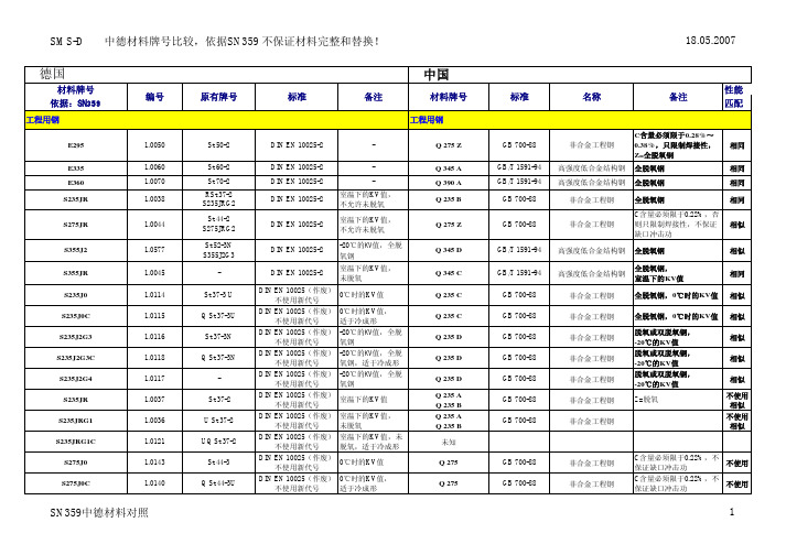
中德材料标准对照-中文
1.0577 1.0045 1.0114 1.0115 1.0116 1.0118 1.0117 1.0037 1.0036 1.0121 1.0143 1.0140
SN359中德材料对照
原有牌号
标准
中国
备注
材料牌号
工程用钢
St 50-2
St 60-2 St 70-2 RSt 37-2 S235JRG2 St 44-2 S275JRG2 St 52-3N S355J2G3
编号
1.0144 1.0141 1.0145 1.0128 1.0553 1.0569
1.0545 1.0546 1.8902 1.8912 1.8901 1.8903
1.0503 1.0401 1.0533
1.0330
原有牌号
St 44-3N Q St 44-3N
Q St 44-2
-
StE 355 TStE 355 StE 420 TStE 420 StE 460 TStE 460
相似 相似 相似 相似 相似 相似
优质碳素结构钢 优质碳素结构钢 非合金工程钢
Z=脱氧 Z=脱氧
相似 相似 相似
优质碳素结构钢
各种情况下都必须检查一 致性
相似
SN359中德材料对照
2
SMS-D 中德材料牌号比较,依据SN359 不保证材料完整和替换!
德国
材料牌号 依据:SN359 管道
P235TR1
C35E+QT
C45+N C45+QT
编号
1.0402 1.0501 1.0501
1.1181 1.0503 1.0503
C45E+QT
1.1191
杰基国际产品说明书
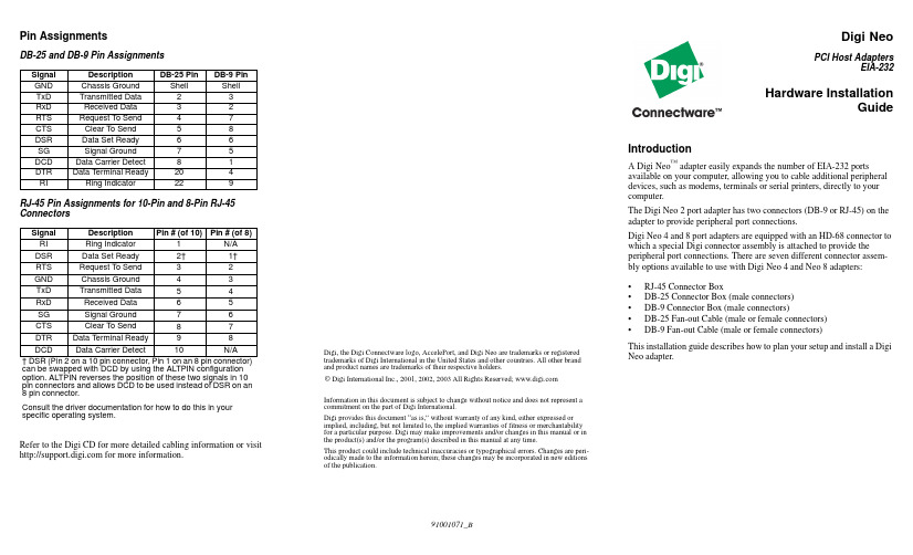
Pin AssignmentsDB-25 and DB-9 Pin AssignmentsRJ-45 Pin Assignments for 10-Pin and 8-Pin RJ-45 ConnectorsRefer to the Digi CD for more detailed cabling information or visit for more information.Digi, the Digi Connectware logo, AccelePort, and Digi Neo are trademarks or registeredtrademarks of Digi International in the United States and other countries. All other brandand product names are trademarks of their respective holders.© Digi International Inc., 2001, 2002, 2003 All Rights Reserved; Information in this document is subject to change without notice and does not represent acommitment on the part of Digi International.Digi provides this document “as is,” without warranty of any kind, either expressed orimplied, including, but not limited to, the implied warranties of fitness or merchantabilityfor a particular purpose. Digi may make improvements and/or changes in this manual or inthe product(s) and/or the program(s) described in this manual at any time.This product could include technical inaccuracies or typographical errors. Changes are peri-odically made to the information herein; these changes may be incorporated in new editionsof the publication.Digi NeoPCI Host AdaptersEIA-232Hardware InstallationGuideIntroductionA Digi Neo™ adapter easily expands the number of EIA-232 portsavailable on your computer, allowing you to cable additional peripheraldevices, such as modems, terminals or serial printers, directly to yourcomputer.The Digi Neo 2 port adapter has two connectors (DB-9 or RJ-45) on theadapter to provide peripheral port connections.Digi Neo 4 and 8 port adapters are equipped with an HD-68 connector towhich a special Digi connector assembly is attached to provide theperipheral port connections. There are seven different connector assem-bly options available to use with Digi Neo 4 and Neo 8 adapters:•RJ-45 Connector Box•DB-25 Connector Box (male connectors)•DB-9 Connector Box (male connectors)•DB-25 Fan-out Cable (male or female connectors)•DB-9 Fan-out Cable (male or female connectors)This installation guide describes how to plan your setup and install a DigiNeo adapter.Signal Description DB-25 Pin DB-9 Pin GND Chassis Ground Shell Shell TxD Transmitted Data23 RxD Received Data32 RTS Request To Send47CTS Clear To Send58DSR Data Set Ready66SG Signal Ground75DCD Data Carrier Detect81DTR Data Terminal Ready204RI Ring Indicator229Signal Description Pin # (of 10)Pin # (of 8)RI Ring Indicator1N/ADSR Data Set Ready2†1†RTS Request To Send32GND Chassis Ground43TxD Transmitted Data54RxD Received Data65SG Signal Ground76CTS Clear To Send87DTR Data Terminal Ready98DCD Data Carrier Detect10N/A† DSR (Pin 2 on a 10 pin connector, Pin 1 on an 8 pin connector)can be swapped with DCD by using the ALTPIN configurationoption. ALTPIN reverses the position of these two signals in 10pin connectors and allows DCD to be used instead of DSR on an8 pin connector.Consult the driver documentation for how to do this in yourspecific operating system.91001071_BStep One: Plan Your SetupA Digi Neo adapter can be set up in a variety of ways. Before you start your installation, consider the following:Number of Components. You can connect two peripheral devices to a Digi Neo 2, up to four peripheral devices to a Digi Neo 4, and eight periph-eral devices to a Digi Neo 8 adapter. Up to four Digi Neo adapters may be installed in a computer.Construction of Cables. To achieve the greatest reliability over distance, cables should be:•Shielded, low capacitance, and preferably designed specifically for serial data transmission.•Grounded at both ends of the cable.•Routed away from noise sources such as generators, motors and fluorescent lights.Cable Connections. Before beginning the installation, verify that you have the appropriate Digi connector assemblies (fan-out cables or connec-tor box assemblies). Fan-out cable and connector box options aredescribed in detail in a separate Cable Usage Guide.You will also need a cable for each peripheral that you will be attach-ing to the connector assembly. The connector type that you need at either end of the peripheral cable depends on the type of Digi connec-tor assembly that you use and the connector on the peripheral.Digi connector assemblies are available with RJ-45, DB-25 or DB-9 connectors. You will need to be sure that you have cables of the cor-rect length and with the right connectors to properly attach thedevices you want to use.Additional information about the Digi Neo adapter, such as specifications and cabling details, is provided on the Digi CD which is packaged with the adapter.Step Two: Install the Neo AdapterCAUTION! To guard against damage to the adapter due to electrostaticdischarge (ESD), do not remove the adapter from its protective packag-ing until you have grounded yourself to the computer chassis (see step 4,below).1.Shut down your computer in the manner recommended for your oper-ating system.2.Unplug power from the computer.3.Remove the computer’s cover.4.Touch the computer chassis to equalize any static potential betweenyourself and the computer. This will help prevent damage to theadapter due to electrostatic discharge.5.Locate an available PCI slot in your computer and remove the slotplate.6.Remove the adapter from its protective packaging.7.Write down the serial number of the adapter in the space providedbelow.8.Insert the adapter into the slot and screw the endplate to the computerchassis. The endplate must be screwed into the computer chassis toremain in compliance with Part 15 of FCC rules.9.Replace the computer’s cover.10.Attach the peripheral interconnect cable(s) to the adapter.CAUTION: Many SCSI adapters use the same HD-68 connector type asthe Neo adapter. Do not plug SCSI devices into the Digi connector, anddo not plug Digi peripheral cables into SCSI adapters.Serial Number: ________________________Step Three: Install Peripheral CablingYou can connect modems, terminals, serial printers, or any other standardEIA-232 device to a Digi Neo adapter using a cable between the periph-eral and the Digi connector assembly.On the peripheral end of the cable, the connector you must have dependson the requirements of the peripheral. The Digi end of the cable must beequipped with the connector type that mates with the connectors on theDigi connector assemblyIn the case of the 2 port product, the cables are connected directly to theadapter’s end-plate.。
j2100a中文规格书
j2100a中文规格书J2100A中文规格书一、产品概述J2100A是一款具有先进功能和性能的电子产品,广泛应用于各个领域。
本规格书旨在详细介绍J2100A的技术规格、特点和使用方法,以便用户能充分了解产品并正确使用。
二、技术规格1. 外观与尺寸:J2100A外形设计简洁大方,尺寸为X mm × Y mm × Z mm(长× 宽× 高),重量为W kg。
2. 屏幕:J2100A配备了高分辨率X英寸LCD显示屏,显示清晰、色彩饱满。
3. 处理器:J2100A采用先进的Z处理器,运行速度快,响应迅速。
4. 存储容量:J2100A内置大容量存储器,可存储大量数据。
5. 电池:J2100A内置高容量电池,续航时间长,使用更加方便。
6. 网络连接:J2100A支持多种网络连接方式,如Wi-Fi、蓝牙等,便于用户进行数据传输和交互。
7. 接口:J2100A具有丰富的接口,包括USB、HDMI、音频接口等,满足各种外设设备的连接需求。
8. 操作系统:J2100A采用先进的操作系统,界面简洁直观,操作便捷。
三、特点功能1. 高性能:J2100A配备了先进的处理器和大容量存储器,运行速度快,处理能力强,能够满足用户对高性能的需求。
2. 多媒体功能:J2100A具备强大的多媒体功能,支持多种音视频格式播放,用户可以随时欣赏高清影片、音乐等。
3. 智能控制:J2100A内置智能控制系统,可通过语音指令或触摸屏操作实现各种功能,操作简便、智能高效。
4. 数据传输:J2100A支持多种数据传输方式,如Wi-Fi、蓝牙等,可方便地与其他设备进行数据传输和共享。
5. 多项应用:J2100A广泛应用于各个领域,如教育、医疗、工业等,能满足不同行业的需求。
6. 安全可靠:J2100A具备严格的安全性能,保护用户数据安全,可靠稳定。
四、使用方法1. 开机:按下电源键,等待片刻,J2100A将自动开机。
MM5ZxxxST1G Serie Zener Voltage Regulators 500 mW
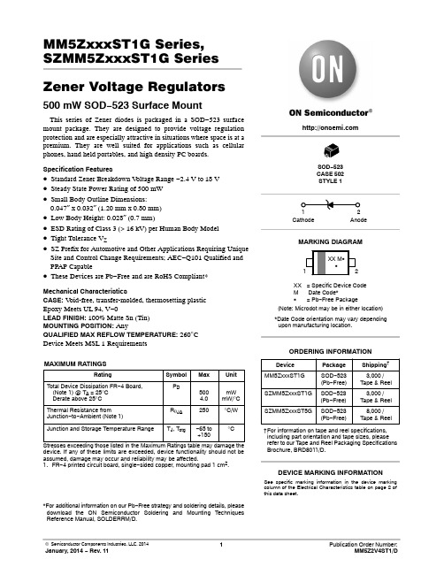
MM5ZxxxST1G Series, SZMM5ZxxxST1G Series Zener Voltage Regulators 500 mW SOD−523 Surface MountThis series of Zener diodes is packaged in a SOD−523 surface mount package. They are designed to provide voltage regulation protection and are especially attractive in situations where space is at a premium. They are well suited for applications such as cellular phones, hand held portables, and high density PC boards. Specification Features•Standard Zener Breakdown V oltage Range −2.4 V to 18 V •Steady State Power Rating of 500 mW•Small Body Outline Dimensions:0.047″ x 0.032″ (1.20 mm x 0.80 mm)•Low Body Height: 0.028″ (0.7 mm)•ESD Rating of Class 3 (> 16 kV) per Human Body Model •Tight Tolerance V Z•SZ Prefix for Automotive and Other Applications Requiring Unique Site and Control Change Requirements; AEC−Q101 Qualified and PPAP Capable•These Devices are Pb−Free and are RoHS Compliant*Mechanical CharacteristicsCASE:V oid-free, transfer-molded, thermosetting plasticEpoxy Meets UL 94, V−0LEAD FINISH: 100% Matte Sn (Tin)MOUNTING POSITION:AnyQUALIFIED MAX REFLOW TEMPERATURE: 260°CDevice Meets MSL 1 RequirementsMAXIMUM RATINGSRating Symbol Max UnitTotal Device Dissipation FR−4 Board, (Note 1) @ T A = 25°CDerate above 25°C P D5004.0mWmW/°CThermal Resistance from Junction−to−Ambient (Note 1)R q JA250°C/WJunction and Storage Temperature Range T J, T stg−65 to+150°CStresses exceeding those listed in the Maximum Ratings table may damage the device. If any of these limits are exceeded, device functionality should not be assumed, damage may occur and reliability may be affected.1.FR−4 printed circuit board, single−sided copper, mounting pad 1 cm2.*For additional information on our Pb−Free strategy and soldering details, please download the ON Semiconductor Soldering and Mounting Techniques Reference Manual, SOLDERRM/D.Device Package Shipping†ORDERING INFORMATIONCathode AnodeSee specific marking information in the device marking column of the Electrical Characteristics table on page 2 of this data sheet.DEVICE MARKING INFORMATIONSOD−523CASE 502STYLE 1MARKING DIAGRAMXX= Specific Device CodeM Date Code*G= Pb−Free Package(Note: Microdot may be in either location)*Date Code orientation may vary dependingupon manufacturing location.MM5ZxxxST1G SOD−523(Pb−Free)3,000 /Tape & Reel†For information on tape and reel specifications, including part orientation and tape sizes, please refer to our T ape and Reel Packaging Specifications Brochure, BRD8011/D.SOD−523(Pb−Free)SZMM5ZxxxST1G3,000 /Tape & ReelSOD−523(Pb−Free)SZMM5ZxxxST5G8,000 /Tape & ReelELECTRICAL CHARACTERISTICS (T A = 25°C unless otherwise noted,V F = 0.9 V Max. @ I F = 10 mA for all types) Symbol Parameter V Z Reverse Zener Voltage @ I ZTI ZT Reverse CurrentZZT Maximum Zener Impedance @ I ZTI ZK Reverse CurrentZ ZK Maximum Zener Impedance @ I ZKI R Reverse Leakage Current @ V RV R Reverse VoltageI F Forward CurrentV F Forward Voltage @ I FQ V Z Maximum Temperature Coefficient of V Z C Max. Capacitance @V R = 0 and f = 1 MHzV Figure 1. Zener Voltage RegulatorELECTRICAL CHARACTERISTICS (V F = 0.9 Max @ I F = 10 mA for all types)Device*DeviceMarkingTestCurrentIzt mAZener VoltageVZZ ZK I Z= 1.0mA WMaxZ ZTI Z = IZT@ 10%Mod WMaxMaxIR @ VRd VZ/dt (mV/k)@ I ZT1 = 5 mA C pF Max @V R = 0f = 1 MHzMin Max m A V Min MaxMM5Z2V4ST1G T2 5.0 2.43 2.631000100120 1.0−3.50450MM5Z2V7ST1G T3 5.0 2.67 2.911000100100 1.0−3.50450MM5Z3V3ST1G T5 5.0 3.32 3.53100095 5.0 1.0−3.50450MM5Z3V6ST1G T6 5.0 3.60 3.85100090 5.0 1.0−3.50450MM5Z3V9ST1G T7 5.0 3.89 4.16100090 3.0 1.0−3.5−2.5450MM5Z4V3ST1G T8 5.0 4.17 4.43100090 3.0 1.0−3.50450MM5Z4V7ST1G/T5G T9 5.0 4.55 4.7580080 3.0 2.0−3.50.2260MM5Z5V1ST1G TA 5.0 4.98 5.250060 2.0 2.0−2.7 1.2225MM5Z5V6ST1G TC 5.0 5.49 5.7320040 1.0 2.0−2.0 2.5200MM5Z6V2ST1G TE 5.0 6.06 6.3310010 3.0 4.00.4 3.7185MM5Z6V8ST1G TF 5.0 6.65 6.9316015 2.0 4.0 1.2 4.5155MM5Z7V5ST1G TG 5.07.287.616015 1.0 5.0 2.5 5.3140MM5Z8V2ST1G TH 5.08.028.36160150.7 5.0 3.2 6.2135MM5Z9V1ST1G TK 5.08.859.23160150.5 6.0 3.87.0130MM5Z12VST1G TN 5.011.7412.2480250.18.0 6.010130MM5Z16VST1G TU 5.015.8516.5180400.0511.210.414105MM5Z18VST1G TW 5.017.5618.3580450.0512.612.416100 Product parametric performance is indicated in the Electrical Characteristics for the listed test conditions, unless otherwise noted. Product performance may not be indicated by the Electrical Characteristics if operated under different conditions.*Include SZ-prefix devices where applicable.TYPICAL CHARACTERISTICSTEMPERATURE (°C)25010040200P O W E R D I S S I P A T I O N (%)50751001251508060Figure 2. Steady State Power DeratingPACKAGE DIMENSIONSSOD −523CASE 502ISSUE ENOTES:1.DIMENSIONING AND TOLERANCING PER ASME Y14.5M, 1994.2.CONTROLLING DIMENSION: MILLIMETERS.3.MAXIMUM LEAD THICKNESS INCLUDES LEAD FINISH.MINIMUM LEAD THICKNESS IS THE MINIMUM THICKNESS OF BASE MATERIAL.4.DIMENSIONS D AND E DO NOT INCLUDE MOLD FLASH, PRO-TRUSIONS, OR GATE BURRS.DIM MIN NOM MAX MILLIMETERS D 1.10 1.20 1.30E 0.700.800.90A 0.500.600.70b 0.250.300.35c 0.070.140.20L 0.30 REF H 1.50 1.60 1.70*For additional information on our Pb −Free strategy and soldering details, please download the ON Semiconductor Soldering and Mounting Techniques Reference Manual, SOLDERRM/D.SOLDERING FOOTPRINT*E RECOMMENDEDSIDE VIEW2XBOTTOM VIEWL2L2X2XL20.150.200.25STYLE 1:PIN 1.CATHODE (POLARITY BAND)2.ANODEON Semiconductor and are registered trademarks of Semiconductor Components Industries, LLC (SCILLC). SCILLC reserves the right to make changes without further notice to any products herein. SCILLC makes no warranty, representation or guarantee regarding the suitability of its products for any particular purpose, nor does SCILLC assume any liability arising out of the application or use of any product or circuit, and specifically disclaims any and all liability, including without limitation special, consequential or incidental damages.“Typical” parameters which may be provided in SCILLC data sheets and/or specifications can and do vary in different applications and actual performance may vary over time. All operating parameters, including “Typicals” must be validated for each customer application by customer’s technical experts. SCILLC does not convey any license under its patent rights nor the rights of others. SCILLC products are not designed, intended, or authorized for use as components in systems intended for surgical implant into the body, or other applications intended to support or sustain life, or for any other application in which the failure of the SCILLC product could create a situation where personal injury or death may occur. Should Buyer purchase or use SCILLC products for any such unintended or unauthorized application, Buyer shall indemnify and hold SCILLC and its officers, employees, subsidiaries, affiliates,and distributors harmless against all claims, costs, damages, and expenses, and reasonable attorney fees arising out of, directly or indirectly, any claim of personal injury or death associated with such unintended or unauthorized use, even if such claim alleges that SCILLC was negligent regarding the design or manufacture of the part. SCILLC is an Equal Opportunity/Affirmative Action Employer. This literature is subject to all applicable copyright laws and is not for resale in any manner.PUBLICATION ORDERING INFORMATION。
ES1J中文资料(Won-Top Electronics)中文数据手册「EasyDatasheet - 矽搜」

A C
B D
F HG E
SMA/DO-214AC
Dim
Min
A
2.50
B
4.00
C
1.20
D
0.152
E
4.80
F
2.00
G
0.051
H
0.76
在毫米所有尺寸
Max 2.90 4.60 1.60 0.305 5.28 2.44 0.203 1.52
最大额定值和电气特性
@TA = 25°C除非另有说明
100
1.0 1.2 1.4
Tj = 25 °C f = 1.0MHz
20 10
10 C,电j 容(pF)
,峰FS值M 正向浪涌电流(A)
I0
1
1
10
100
1
10
100
循环次数在60Hz
VR,反向电压(V)
图. 3峰值正向浪涌电流
图. 4典型结电容
50Ω NI(非感性)
10Ω NI
trr +0.5A
0
0 25 50 75 100 125 150 175
T L ,焊接温度 图. 1正向电流降额曲线
( ° C)
30
Pulse width 8.3 ms single half-sine-wave
(JEDEC method)
,正F 向电流(A) I 0.01
0 0.2 0.4 0.6 0.8
VF,正向电压(V) 图. 2典型正向特性
出货数量
7500 /磁带和卷轴 7500 /磁带和卷轴 7500 /磁带和卷轴 7500 /磁带和卷轴 7500 /磁带和卷轴 7500 /磁带和卷轴 7500 /磁带和卷轴
淼田电子有限公司LQG15HH系列芯片电感说明书
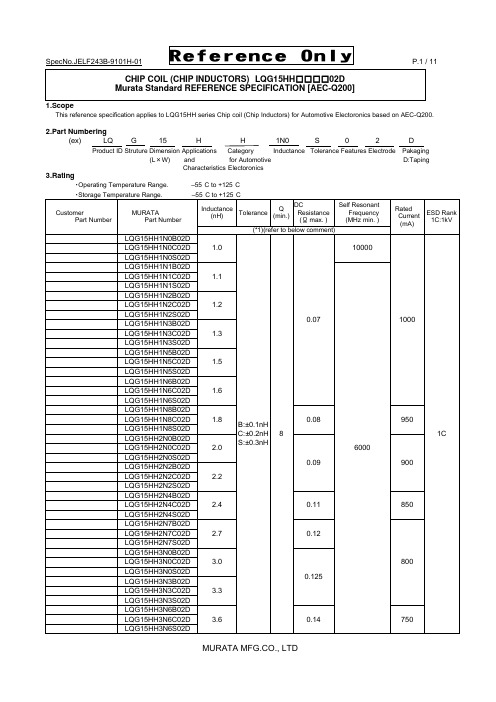
SpecNo.JELF243B-9101H-01 P.1 / 11Reference OnlyCHIP COIL (CHIP INDUCTORS) LQG15HH □□□□02DMurata Standard REFERENCE SPECIFICATION [AEC-Q200]1.ScopeThis reference specification applies to LQG15HH series Chip coil (Chip Inductors) for Automotive Electoronics based on AEC-Q200.2.Part Numbering(ex) LQ G 15 H H 1N0 S 0 2 DProduct ID Struture Dimension Applications Category Inductance Tolerance Features Electrode Pakaging(L ×W) and for Automotive D:TapingCharacteristics Electoronics3.Rating・Operating Temperature Range. –55°C to +125°C ・Storage Temperature Range. –55°C to +125°CCustomer Part Number MURATAPart NumberInductance (nH) ToleranceQ(min.)DC Resistance (Ω max. ) Self ResonantFrequency (MHz min. )Rated Current (mA)ESD Rank 1C:1kV(*1)(refer to below comment)LQG15HH1N0B02D1.0B:±0.1nHC:±0.2nH S:±0.3nH8 0.07 10000 10001CLQG15HH1N0C02D LQG15HH1N0S02D LQG15HH1N1B02D1.1 6000 LQG15HH1N1C02DLQG15HH1N1S02D LQG15HH1N2B02D 1.2 LQG15HH1N2C02D LQG15HH1N2S02DLQG15HH1N3B02D1.3 LQG15HH1N3C02DLQG15HH1N3S02D LQG15HH1N5B02D1.5 LQG15HH1N5C02DLQG15HH1N5S02D LQG15HH1N6B02D 1.6 LQG15HH1N6C02D LQG15HH1N6S02D LQG15HH1N8B02D 1.8 0.08 950LQG15HH1N8C02D LQG15HH1N8S02DLQG15HH2N0B02D2.0 0.09 900LQG15HH2N0C02DLQG15HH2N0S02DLQG15HH2N2B02D 2.2 LQG15HH2N2C02D LQG15HH2N2S02D LQG15HH2N4B02D2.4 0.11 850 LQG15HH2N4C02DLQG15HH2N4S02D LQG15HH2N7B02D 2.7 0.12 800 LQG15HH2N7C02D LQG15HH2N7S02D LQG15HH3N0B02D 3.0 0.125LQG15HH3N0C02D LQG15HH3N0S02DLQG15HH3N3B02D3.3 LQG15HH3N3C02DLQG15HH3N3S02D LQG15HH3N6B02D3.6 0.14 750 LQG15HH3N6C02DLQG15HH3N6S02DCustomer Part Number MURATAPart NumberInductance (nH) ToleranceQ(min.)DC Resistance (Ω max. ) Self ResonantFrequency(MHz min. )RatedCurrent(mA)ESD Rank 1C:1kV(*1)(refer to below comment)LQG15HH3N9B02D3.9 B:±0.1nHC:±0.2nHS:±0.3nH8 0.14 6000 7501CLQG15HH3N9C02DLQG15HH3N9S02DLQG15HH4N3B02D 4.3 LQG15HH4N3C02D LQG15HH4N3S02D LQG15HH4N7B02D 4.7 0.16 700LQG15HH4N7C02D LQG15HH4N7S02DLQG15HH5N1B02D5.1 0.18 5300 650LQG15HH5N1C02DLQG15HH5N1S02DLQG15HH5N6B02D5.6 4500 LQG15HH5N6C02DLQG15HH5N6S02D LQG15HH6N2B02D6.2 0.20 600LQG15HH6N2C02DLQG15HH6N2S02DLQG15HH6N8G02D6.8 G:±2%H:±3%J:±5%0.22 LQG15HH6N8H02DLQG15HH6N8J02D LQG15HH7N5G02D 7.5 0.24 4200 550LQG15HH7N5H02D LQG15HH7N5J02DLQG15HH8N2G02D 8.2 3700 LQG15HH8N2H02D LQG15HH8N2J02DLQG15HH9N1G02D 9.1 0.26 3400500LQG15HH9N1H02D LQG15HH9N1J02DLQG15HH10NG02D10 LQG15HH10NH02D LQG15HH10NJ02D LQG15HH12NG02D12 0.28 3000 LQG15HH12NH02DLQG15HH12NJ02DLQG15HH15NG02D15 0.32 2500 450 LQG15HH15NH02DLQG15HH15NJ02D LQG15HH18NG02D18 0.36 2200 400 LQG15HH18NH02DLQG15HH18NJ02D LQG15HH22NG02D 22 0.42 1900 350 LQG15HH22NH02D LQG15HH22NJ02D LQG15HH27NG02D 27 0.46 1700 LQG15HH27NH02D LQG15HH27NJ02D LQG15HH33NG02D33 0.58 1600 LQG15HH33NH02DLQG15HH33NJ02D LQG15HH39NG02D39 0.65 1200 300 LQG15HH39NH02DLQG15HH39NJ02DCustomer Part Number MURATAPart NumberInductance (nH) Tolerance Q(min.) DC Resistance (Ω max. ) Self Resonant Frequency (MHz min. )Rated Current (mA)ESD Rank 1C:1kV(*1)(refer to below comment)LQG15HH47NG02D 47 G:±2%H:±3%J:±5%8 0.72 1000 3001CLQG15HH47NH02D LQG15HH47NJ02DLQG15HH56NG02D 56 0.82 800 250LQG15HH56NH02D LQG15HH56NJ02DLQG15HH68NG02D68 0.92 LQG15HH68NH02DLQG15HH68NJ02D LQG15HH82NG02D82 1.20 700 200 LQG15HH82NH02DLQG15HH82NJ02D LQG15HHR10G02D100 1.25 600 LQG15HHR10H02DLQG15HHR10J02DLQG15HHR12G02D120 1.30 LQG15HHR12H02DLQG15HHR12J02DLQG15HHR15G02D 150 2.99 550 150LQG15HHR15H02D LQG15HHR15J02DLQG15HHR18G02D 180 3.38 500 LQG15HHR18H02D LQG15HHR18J02D LQG15HHR22G02D 220 3.77 450 120 LQG15HHR22H02D LQG15HHR22J02D LQG15HHR27G02D270 4.94 400 110 LQG15HHR27H02DLQG15HHR27J02D(*1) Standard Testing Conditions《Unless otherwise specified 》 《In case of doubt 》Temperature : Ordinary Temperature / 15°C to 35°C Temperature: 20°C ± 2°CHumidity :Ordinary Humidity / 25%(RH) to 85%(RH) Humidity : 60%(RH) to 70%(RH) Atmospheric Pressure : 86kPa to 106 kPa4. Appearance and Dimensions■Unit Mass (Typical value)6.Q200 Requirement6.1.Performance (based on Table 5 for Magnetics(Inductors / Transformer)AEC-Q200 Rev.D issued June 1. 2010AEC-Q200 Murata Specification / Deviation No Stress TestMethod3 HighTemperatureExposure 1000hours at 125 deg CSet for 24hours at roomtemperature, then measured.Meet Table A after testing.Table A4 TemperatureCycling 1000cycles-40 deg C to +125 deg CSet for 24hours at roomtemperature,thenmeasured.Meet Table A after testing.7 Biased Humidity 1000hours at 85 deg C, 85%RHunpowered.Meet Table A after testing.8 Operational Life Apply 125 deg C 1000hoursSet for 24hours at roomtemperature, then measuredMeet Table A after testing.9 External Visual Visual inspection No abnormalities10 Physical Dimension Meet ITEM 4(Style and Dimensions)No defects12 Resistanceto Solvents PerMIL-STD-202Method 215Not ApplicableAppearance No damageInductanceChange(at 100MHz)Within ±10%AEC-Q200 Murata Specification / Deviation No Stress TestMethod13 Mechanical Shock Per MIL-STD-202Method 213Condition C : 100g’s(0.98N),6ms, Half sine, 12.3ft/sMeet Table A after testing.14 Vibration 5g's(0.049N) for 20 minutes,12cycles each of 3 oritentationsTest from 10-2000Hz.Meet Table A after testing.15 Resistanceto Soldering Heat No-heatingSolder temperature260C+/-5 deg CImmersion time 10sMeet Table A after testing.Pre-heating 150C +/-10 deg C, 60s to 90s17 ESD Per AEC-Q200-002 ESD Rank: refer to the Item3 (Rating).Meet Table A after testing18 Solderbility Per J-STD-002 Method b : Not Applicable90% of the terminations is to be soldered.19 ElectricalCharacterizationMeasured : Inductance No defects20 Flammability Per UL-94 Not Applicable21 Board Flex Epoxy-PCB(1.6mm)Deflection 2mm(min)Holding time 60s Meet Table B after testing.Table BAppearance No damage DCresistanceChangeWithin ±10%22 Terminal Strength Per AEC-Q200-006A force of 17.7Nfor 60s Murata Deviation Request: 5N No defects7.Specification of Packaging(in mm)7.2 Specification of Taping(1) Packing quantity (standard quantity)10,000 pcs. / reel(2) Packing MethodProducts shall be packed in the cavity of the base tape and sealed by top tape and bottom tape.(3) Sprocket holeThe sprocket holes are to the right as the tape is pulled toward the user.(4) Spliced pointBase tape and Top tape has no spliced point.(5) Missing components numberMissing components number within 0.1 % of the number per reel or 1 pc., whichever is greater,andare not continuous. The Specified quantity per reel is kept.0.8m ax.7.3 Pull StrengthTop tape5N min.Bottom tape7.4 Peeling off force of cover tapeSpeed of Peeling off 300mm/min Peeling off force0.1N to 0.6N(minimum value is typical)7.5 Dimensions of Leader-tape,Trailer and ReelThere shall be leader-tape ( top tape and empty tape) and trailer-tape (empty tape) as follows.7.6 Marking for reelCustomer part number, MURATA part number, Inspection number(*1) ,RoHS Marking(*2), Quantity etc ・・・*1) <Expression of Inspection No.> □□ OOOO ⨯⨯⨯(1) (2) (3)(1) Factory Code (2) Date First digit : Year / Last digit of yearSecond digit: Month / Jan. to Sep. → 1 to 9, Oct. to Dec. → O, N, D Third, Fourth digi : Day(3) Serial No.*2) <Expression of RoHS Marking> ROHS – Y (△)(1) (2)(1) RoHS regulation conformity parts. (2) MURATA classification number7.7 Marking for Outside package (corrugated paper box)Customer name, Purchasing order number, Customer part number, MURATA part number, RoHS Marking(*2) ,Quantity, etc ・・・7.8. Specification of Outer CaseOuter Case Dimensions(mm)Standard Reel Quantityin Outer Case (Reel)W D H 186 186 93 5* Above Outer Case size is typical. It depends on a quantity of an order.F165to 180degreeTop tape Bottom tapeBase tapeWDLabelH8. △!Caution8.1 Caution(Rating)Do not exceed maximum rated current of the product. Thermal stress may be transmitted to the product and short/open circuit of the product or falling off the product may be occurred.8.2 Fail-safe Be sure to provide an appropriate fail-safe function on your product to prevent a second damage that may becaused by the abnormal function or the failure of our product.8.3 Limitation of ApplicationsPlease contact us before using our products for the applications listed below which require especially high reliability for the prevention of defects which might directly cause damage to the third party's life, body or property.(1) Aircraft equipment (6) Transportation equipment (trains, ships, etc.) (2) Aerospace equipment (7) Traffic signal equipment(3) Undersea equipment (8) Disaster prevention / crime prevention equipment (4) Power plant control equipment (9) Data-processing equipment (5) Medical equipment (10) Applications of similar complexity and /or reliability requirements to the applications listed in the above9. NoticeProducts can only be soldered with reflow. This product is designed for solder mounting.Please consult us in advance for applying other mounting method such as conductive adhesive.9.1 Land pattern designinga 0.4b 1.4 to 1.5c 0.5 to 0.6(in mm)9.2 Flux, Solder・Use rosin-based flux.Don’t use highly acidic flux with halide content exceeding 0.2(wt)% (chlorine conversion value). Don’t use water-soluble flux. ・Use Sn-3.0Ag-0.5Cu solder.・Standard thickness of solder paste : 100μm to 150μm.Resist9.3 Reflow soldering conditions・Inductance value may be changed a little due to the amount of solder.So, the chip coil shall be soldered by reflow so that the solder volume can be controlled.・Pre-heating should be in such a way that the temperature difference between solder and product surface is limited to 150°C max. Cooling into solvent after soldering also should be in such a way that the temperature difference is limited to 100°C max.Insufficient pre-heating may cause cracks on the product, resulting in the deterioration of products quality. ・Standard soldering profile and the limit soldering profile is as follows.The excessive limit soldering conditions may cause leaching of the electrode and / or resulting in the deterioration of product quality.・Reflow soldering profileStandard Profile Limit Profile Pre-heating 150°C ~180°C 、90s ±30s Heating above 220°C 、30s ~60s above 230°C 、60s max. Peak temperature 245°C ±3°C 260°C,10s Cycle of reflow 2 times 2 times9.4 Reworking with soldering ironThe following conditions must be strictly followed when using a soldering iron.Pre-heating 150°C,1 min Tip temperature 350°C max. Soldering iron output 80W max. Tip diameter φ3mm max. Soldering time 3(+1,-0)sTime 2 timesNote :Do not directly touch the products with the tip of the soldering iron in order to prevent the crack on the products due to the thermal shock.9.5 Solder Volume・ Solder shall be used not to be exceed the upper limits as shown below.・ Accordingly increasing the solder volume, the mechanical stress to Chip is also increased. Exceeding solder volume may cause the failure of mechanical or electrical performance.1/3T ≦t ≦TT :thickness of product9.6 Mount ShockOver Mechanical stress to products at mounting process causes crack and electrical failure etc.Limit ProfileStandard Profile 90s±30s 230℃260℃245℃±3℃220℃30s~60s 60s max.180150Temp.(s)(℃)Time.9.7 Product’s locationThe following shall be considered when designing and laying out P.C.B.'s.(1) P.C.B. shall be designed so that products are not subjected to the mechanical stress due to warping the board.[Products direction ]Products shall be located in the sideways direction (Length:a <b) to the mechanical stress.(2) Components location on P.C.B. separation. It is effective to implement the following measures, to reduce stress in separating the board.It is best to implement all of the following three measures; however, implement as many measures as possible to reduce stress.Contents of MeasuresStress Level (1) Turn the mounting direction of the component parallel to the board separation surface. A > D *1 (2) Add slits in the board separation part.A >B (3) Keep the mounting position of the component away from the board separation surface. A > C*1 A > D is valid when stress is added vertically to the perforation as with Hand Separation.If a Cutting Disc is used, stress will be diagonal to the PCB, therefore A > D is invalid.(3) Mounting Components Near Screw HolesWhen a component is mounted near a screw hole, it may be affected by the board deflection that occurs during the tightening of the screw. Mount the component in a position as far away from the screw holes as possible.9.8 Cleaning ConditionsProducts shall be cleaned on the following conditions.(1) Cleaning temperature shall be limited to 60°C max.(40°C max for IPA.)(2) Ultrasonic cleaning shall comply with the following conditions with avoiding the resonance phenomenon at the mounted products and P.C.B.Power : 20 W / l max. Frequency : 28kHz to 40kHz Time : 5 min max.(3) Cleaner1. Alcohol type cleanerIsopropyl alcohol (IPA)2. Aqueous agentPINE ALPHA ST-100S(4) There shall be no residual flux and residual cleaner after cleaning. In the case of using aqueous agent, products shall be dried completely after rinse with de-ionized water in order to remove the cleaner. (5) Other cleaning Please contact us.〈Poor example 〉〈Good example 〉ba9.9 Resin coatingThe inductance value may change and/or it may affect on the product's performance due to highcure-stress of resin to be used for coating / molding products. So please pay your careful attention whenyou select resin.In prior to use, please make the reliability evaluation with the product mounted in your application set.9.10 Handling of a substrateAfter mounting products on a substrate, do not apply any stress to the product caused by bending ortwisting to the substrate when cropping the substrate, inserting and removing a connector from thesubstrate or tightening screw to the substrate.Excessive mechanical stress may cause cracking in the product.Bending Twisting9.11 Storage and Handing Requirements(1) Storage periodUse the products within 6 months after deliverd.Solderability should be checked if this period is exceeded.(2) Storage conditions・Products should be stored in the warehouse on the following conditions.Temperature: -10°C to 40°CHumidity: 15% to 85% relative humidity No rapid change on temperature and humidityDon't keep products in corrosive gases such as sulfur,chlorine gas or acid, or it may causeoxidization of electrode, resulting in poor solderability.・Products should be storaged on the palette for the prevention of the influence from humidity, dust and so on.・Products should be storaged in the warehouse without heat shock, vibration, direct sunlight and so on.・Products should be storaged under the airtight packaged condition.(3) Handling ConditionCare should be taken when transporting or handling product to avoid excessive vibration or mechanical shock.10.△!Note(1) Please make sure that your product has been evaluated in view of your specifications with our product being mounted to your product.(2) You are requested not to use our product deviating from the reference specifications.(3) The contents of this reference specification are subject to change without advance notice.Please approve our product specifications or transact the approval sheet for product specificationsbefore ordering.Reference OnlySpecNo.JELF243B-9101H-01 P.11 / 11。
毛斯(Moxa)UC-8200系列双核ARM Cortex-A7 1GHz IIoT网关产品说明书
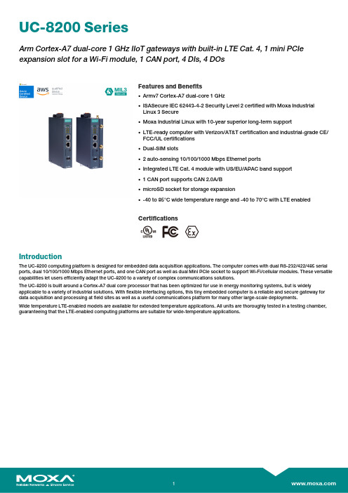
UC-8200SeriesArm Cortex-A7dual-core1GHz IIoT gateways with built-in LTE Cat.4,1mini PCIe expansion slot for a Wi-Fi module,1CAN port,4DIs,4DOsFeatures and Benefits•Armv7Cortex-A7dual-core1GHz•ISASecure IEC62443-4-2Security Level2certified with Moxa IndustrialLinux3Secure•Moxa Industrial Linux with10-year superior long-term support•LTE-ready computer with Verizon/AT&T certification and industrial-grade CE/FCC/UL certifications•Dual-SIM slots•2auto-sensing10/100/1000Mbps Ethernet ports•Integrated LTE Cat.4module with US/EU/APAC band support•1CAN port supports CAN2.0A/B•microSD socket for storage expansion•-40to85°C wide temperature range and-40to70°C with LTE enabledCertificationsIntroductionThe UC-8200computing platform is designed for embedded data acquisition applications.The computer comes with dual RS-232/422/485serial ports,dual10/100/1000Mbps Ethernet ports,and one CAN port as well as dual Mini PCIe socket to support Wi-Fi/cellular modules.These versatile capabilities let users efficiently adapt the UC-8200to a variety of complex communications solutions.The UC-8200is built around a Cortex-A7dual core processor that has been optimized for use in energy monitoring systems,but is widely applicable to a variety of industrial solutions.With flexible interfacing options,this tiny embedded computer is a reliable and secure gateway for data acquisition and processing at field sites as well as a useful communications platform for many other large-scale deployments.Wide temperature LTE-enabled models are available for extended temperature applications.All units are thoroughly tested in a testing chamber, guaranteeing that the LTE-enabled computing platforms are suitable for wide-temperature applications.AppearanceUC-8210UC-8220SpecificationsComputerCPU Armv7Cortex-A7dual-core1GHzDRAM2GB DDR3LSupported OS Moxa Industrial Linux1(Debian9,kernel4.4),2027EOLMoxa Industrial Linux31(Debian11,kernel5.10),2031EOLSee /MILStorage Pre-installed8GB eMMCExpansion Slots MicroSD(SD3.0)socket x13OS is selectable via Moxa Computer Configuration System(CCS)for CTO models.For the model names,see the Ordering Information section of thedatasheet PDF file.Computer InterfaceEthernet Ports Auto-sensing10/100/1000Mbps ports(RJ45connector)x2 Serial Ports RS-232/422/485ports x2,software selectable(DB9male) CAN Ports CAN2.0A/B x1(DB9male)Digital Input DIs x4Digital Output DOs x4USB2.0USB2.0hosts x1,type-A connectorsWi-Fi Antenna Connector UC-8220Models:RP-SMA x2Cellular Antenna Connector UC-8220Models:SMA x2GPS Antenna Connector UC-8220Models:SMA x1Expansion Slots UC-8220-T-LX:mPCIe slot x2UC-8220-T-LX US/EU/AP Models:mPCIe slot x1SIM Format UC-8220Models:NanoNumber of SIMs UC-8220Models:2Buttons Programmable buttonTPM TPM v2.0Ethernet InterfaceMagnetic Isolation Protection 1.5kV(built-in)Security FunctionsHardware-based Security TPM2.0Hardware Root of Trust Secure BootIntrusion Detection Host-based Intrusion DetectionSecurity Tools Security Diagnostic ToolSecurity Event AuditingSecure UpdateDisk Protection LUKS Disk EncryptionRecovery One-step recovery to the last known secure stateDual-system design with automatic failbackReliability Network Keep AliveNetwork Failover and FailbackSerial InterfaceBaudrate300bps to921.6kbpsData Bits7,8Stop Bits1,2Parity None,Even,Odd,Space,MarkFlow Control RTS/CTS,XON/XOFFADDC(automatic data direction control)for RS-485RTS Toggle(RS-232only)Console Port1x4-pin header to DB9console portRS-232TxD,RxD,RTS,CTS,DTR,DSR,DCD,GNDRS-422Tx+,Tx-,Rx+,Rx-,GNDRS-485-2w Data+,Data-,GNDCAN InterfaceNo.of Ports1Connector DB9maleBaudrate10to1000kbpsIndustrial Protocols CAN2.0ACAN2.0BIsolation2kV(built-in)Signals CAN_H,CAN_L,CAN_GND,CAN_SHLD,CAN_V+,GNDDigital InputsConnector Screw-fastened Euroblock terminalDry Contact Off:openOn:short to GNDIsolation3K VDCSensor Type Wet contact(NPN)Dry contactWet Contact(DI to COM)On:10to30VDCOff:0to3VDCDigital OutputsConnector Screw-fastened Euroblock terminalCurrent Rating200mA per channelI/O Type SinkVoltage24VDC nominal,open collector to30VDCCellular InterfaceCellular Standards LTE Cat.4Band Options US Models:LTE Band2(1900MHz)/LTE Band4(1700MHz)/LTE Band5(850MHz)/LTE Band13(700MHz)/LTE Band17(700MHz)UMTS/HSPA850MHz/1900MHzCarrier Approval:Verizon,AT&TEU Models:LTE Band1(2100MHz)/LTE Band3(1800MHz)/LTE Band5(850MHz)/LTE Band7(2600MHz)/LTE Band8(900MHz)/LTE Band20(800MHz)UMTS/HSPA850MHz/900MHz/1900MHz/2100MHzAP Models:LTE Band1(2100MHz)/LTE Band3(1800MHz)/LTE Band5(850MHz)/LTE Band7(2600MHz)/LTE Band8(900MHz)/LTE Band28(700MHz)UMTS/HSPA850MHz/900MHz/1900MHz/2100MHzReceiver Types GPS/GLONASS/GalileoState-of-the-art GNSS solutionAccuracy Position:2.0m@CEP50Acquisition Hot starts:1.1secCold starts:29.94secSensitivity Cold starts:-145dBmTracking:-160dBmTime Pulse0.25Hz to10MHzLED IndicatorsSystem Power x2Programmable x1SIM card indicator x1Wireless Signal Strength Cellular/Wi-Fi x6Power ParametersNo.of Power Inputs Redundant dual inputsInput Voltage12to48VDCPower Consumption10WInput Current0.8A@12VDCReliabilityAlert Tools External RTC(real-time clock)Automatic Reboot Trigger External WDT(watchdog timer)Physical CharacteristicsDimensions UC-8220Models:141.5x120x39mm(5.7x4.72x1.54in)UC-8210Models:141.5x120x27mm(5.7x4.72x1.06in)141.5x120x27mm(5.7x4.72x1.06in)Weight UC-8210Models:560g(1.23lb)UC-8220Models:750g(1.65lb)Housing SECCMetalIP Rating IP30Installation DIN-rail mountingWall mounting(with optional kit)Environmental LimitsOperating Temperature-40to70°C(-40to158°F)Storage Temperature(package included)-40to85°C(-40to185°F)Ambient Relative Humidity5to95%(non-condensing)Shock IEC60068-2-27Vibration2Grms@IEC60068-2-64,random wave,5-500Hz,1hr per axis(without USB devicesattached)Standards and CertificationsEMC EN55032/35EN61000-6-2/-6-4EMI CISPR32,FCC Part15B Class AEMS IEC61000-4-2ESD:Contact:4kV;Air:8kVIEC61000-4-3RS:80MHz to1GHz:10V/mIEC61000-4-4EFT:Power:2kV;Signal:1kVIEC61000-4-6CS:10VIEC61000-4-8PFMFIEC61000-4-5Surge:Power:0.5kV;Signal:1kV Industrial Cybersecurity IEC62443-4-1IEC62443-4-2Hazardous Locations Class I Division2ATEXIECExCarrier Approvals VerizonAT&TSafety UL62368-1EN62368-1Green Product RoHS,CRoHS,WEEEMTBFTime UC-8210-T-LX-S:708,581hrsUC-8220-T-LX:650,836hrsUC-8220-T-LX-US-S/EU-S/AP-S:528,574hrs Standards Telcordia(Bellcore)Standard TR/SRWarrantyWarranty Period5yearsDetails See /warrantyPackage ContentsDevice1x UC-8200Series computerDocumentation1x quick installation guide1x warranty cardInstallation Kit1x DIN-rail kit(preinstalled)1x power jack6x M2.5mounting screws for the cellular module Cable1x console cableDimensions UC-8210UC-8220Ordering Information12UC-8210-T-LX-SDefault:MIL1(-Debian9),2027EOLOrder WithModel UC-8210-T-LX-S(CTO):MIL3(Debian11)Secure/Standard,2031EOLWith MIL3Secure1GHzDual CoreBuilt in––-40to85°CUC-8220-T-LXDefault:MIL1(-Debian9),2027EOLOrder WithModel UC-8220-T-LX(CTO):MIL3(Debian11)Secure/Standard,2031EOLWith MIL3Secure1GHzDual CoreBuilt in Reserved Reserved-40to70°CUC-8220-T-LX-US-SDefault:MIL1(-Debian9),2027EOLOrder WithModel UC-8220-T-LX-US-S(CTO):MIL3(Debian11)Secure/Standard,2031EOLWith MIL3Secure1GHzDual CoreBuilt inUS region LTEmodulepreinstalledReserved-40to70°CUC-8220-T-LX-EU-SDefault:MIL1(-Debian9),2027EOLOrder WithModel UC-8220-T-LX-EU-S(CTO):MIL3(Debian11)Secure/Standard,2031EOLWith MIL3Secure1GHzDual CoreBuilt inEurope regionLTE modulepreinstalledReserved-40to70°CUC-8220-T-LX-AP-SDefault:MIL1(-Debian9),2027EOLOrder WithModel UC-8220-T-LX-AP-S(CTO):MIL3(Debian11)Secure/Standard,2031EOLWith MIL3Secure1GHzDual CoreBuilt inAPAC regionLTE modulepreinstalledReserved-40to70°CUC-8210-T-LX-S(CTO)MIL3(Debian11)Secure orStandard,2031EOLWith MIL3Secure1GHzDual CoreBuilt in––-40to85°CUC-8220-T-LX(CTO)MIL3(Debian11)Secure orStandard,2031EOLWith MIL3Secure1GHzDual Core–Reserved Reserved-40to70°CUC-8220-T-LX-US-S (CTO)MIL3(Debian11)Secure orStandard,2031EOLWith MIL3Secure1GHzDual CoreBuilt inUS region LTEmodulepreinstalledReserved-40to70°C12UC-8220-T-LX-EU-S (CTO)MIL3(Debian11)Secure orStandard,2031EOLWith MIL3Secure1GHzDual CoreBuilt inEurope regionLTE modulepreinstalledReserved-40to70°CUC-8220-T-LX-AP-S (CTO)MIL3(Debian11)Secure orStandard,2031EOLWith MIL3Secure1GHzDual CoreBuilt inAPAC regionLTE modulepreinstalledReserved-40to70°CAccessories(sold separately)Power AdaptersPWR-12150-EU-SA-T Locking barrel plug,12VDC,1.5A,100to240VAC,EU plug,-40to75°C operating temperature PWR-12150-UK-SA-T Locking barrel plug,12VDC,1.5A,100to240VAC,UK plug,-40to75°C operating temperature PWR-12150-USJP-SA-T Locking barrel plug,12VDC1.5A,100to240VAC,US/JP plug,-40to75°C operating temperature PWR-12150-AU-SA-T Locking barrel plug,12VDC,1.5A,100to240VAC,AU plug,-40to75°C operating temperature PWR-12150-CN-SA-T Locking barrel plug,12VDC,1.5A,100to240VAC,CN plug,-40to75°C operating temperature Power WiringCBL-PJTB-10Non-locking barrel plug to bare-wire cableCablesCBL-F9DPF1x4-BK-100Console cable with4-pin connector,1mWi-Fi Wireless ModulesUC-8200-WLAN22-AC Wireless package for UC-8200V2.0or later with Wi-Fi module,2screws,2spacers,1heat sink,1pad AntennasANT-LTEUS-ASM-01GSM/GPRS/EDGE/UMTS/HSPA/LTE,1dBi,omnidirectional rubber-duck antennaANT-LTE-ASM-04BK704to960/1710to2620MHz,LTE omnidirectional stick antenna,4.5dBiANT-LTE-OSM-03-3m BK700-2700MHz,multiband antenna,specifically designed for2G,3G,and4G applications,3m cable ANT-LTE-ASM-05BK704-960/1710-2620MHz,LTE stick antenna,5dBiANT-LTE-OSM-06-3m BK MIMO Multiband antenna with screw-fastened mounting option for700-2700/2400-2500/5150-5850MHzfrequenciesANT-WDB-ARM-02022dBi at2.4GHz or2dBi at5GHz,RP-SMA(male),dual-band,omnidirectional antennaDIN-Rail Mounting KitsUC-8210DIN-rail Mounting Kit DIN-rail mounting kit for UC-8210with4M3screwsUC-8220DIN-rail Mounting Kit DIN-rail mounting kit for UC-8220with4M3screwsWall-Mounting KitsUC-8200Wall-mounting Kit Wall-mounting kit for UC-8200with4M3screws©Moxa Inc.All rights reserved.Updated Jul18,2023.This document and any portion thereof may not be reproduced or used in any manner whatsoever without the express written permission of Moxa Inc.Product specifications subject to change without notice.Visit our website for the most up-to-date product information.。
G.SKILL DDR3内存型号参考清单说明书

G.SKILL F3-3000C12Q-16GTXDG16GB (4 x 4GB )SS--- 1.65V●●●G.SKILL F3-2933C12D-8GTXDG8GB (2 x 4GB )SS--12-14-14-35 1.65V●●G.SKILL F3-2933C12Q-16GTXDG16GB (4 x 4GB )SS--12-14-14-35 1.65V●●●G.SKILL F3-2800C11Q-16GTXD(XMP)16GB(4GBx4)DS--11-13-13-35 1.65V●●CORSAIR CMD16GX3M4A2666C11 (XMP)4GB DS--11-13-13-35 1.65V●●●G.SKILL F3-2666C11Q-16GTXD(XMP)16GB(4GBx4)DS--11-13-13-35 1.65V●●●Team TXD34G2666HC11CBK8GB ( 2x 4GB )SS--11-13-13-35 1.65V●●●Team TXD38G2666HC11CBK16GB ( 2x 8GB )DS--11-13-13-35 1.65V●●G.SKILL F3-2600CL10Q-16GBZMD(XMP)16GB(4x 4GB)DS--10-12-12-31 1.65V●●G.SKILL F3-2600CL11Q-32GBZHD(XMP)32GB(8GBX4)DS--11-13-13-35 1.65V●●ADATA AX3U2600GW8G1116GB ( 2x 8GB )DS--11-13-13-35 1.65V●●CORSAIR CMGTX8(XMP)8GB (2GBx 4)SS--10-12-10-27 1.65V●●G.SKILL F3-2400C10D-8GTX(XMP)8GB(2x 4GB)SS--10-12-12-31 1.65V●●●G.SKILL F3-19200CL11Q-16GBZHD(XMP1.3)16GB ( 4GB x4 )DS--11-11-11-31 1.65V●●G.SKILL F3-19200CL 10Q-32GBZHD(XMP)8GB DS--10-12-12-31 1.65V●●●KINGMAX FLLE88F-C8KKAA HAIS(XMP)2GB SS--10-11-10-30 1.8V●●●KINGSTON KHX24C11T2K2/8X(XMP)4GB DS--- 1.65V●●●ADATA AX3U2400GW8G1116GB ( 2x 8GB )DS--11-13-13-35 1.65V●●ADATA AX3U2400G4G10-DG2(XMP)4GB DS--10-12-12-31 1.65V●●Team TXD38G2400HC10QBK8GB DS--10-12-12-31 1.65V●●●KINGSTON KHX2250C9D3T1K2/4GX(XMP)4GB ( 2x 2GB )DS--- 1.65V●●●GEIL GET34GB2200C9DC(XMP)2GB DS--9-10-9-28 1.65V●●GEIL GET38GB2200C9ADC(XMP)4GB DS--9-11-9-28 1.65V●●KINGMAX FLKE85F-B8KJAA-FEIS(XMP)2GB DS--- 1.5V●●CORSAIR CMT16GX3M4X2133C9(XMP 1.3)16GB ( 4GB x4 )DS--9-11-10-27 1.50V●●●CORSAIR CMT4GX3M2A2133C9(XMP)4GB(2x 2GB)DS--9-10-9-24 1.65V●●●CORSAIR CMT4GX3M2B2133C9(XMP)4GB(2x 2GB)DS--9-10-9-27 1.50V●CORSAIR CMT8GX3M2B2133C9(XMP)8GB ( 4GB x 2)DS--9-11-9-27 1.50V●●●G.SKILL F3-17000CL9Q-16GBZH(XMP1.3)16GB ( 4GB x4 )DS--9-11-10-28 1.65V●●●G.SKILL F3-17000CL11Q2-64GBZLD(XMP)8GB DS--11-11-11-31 1.5V●●●G.SKILL F3-2133C11Q-32GZL(XMP)8GB DS--11-11-11-31 1.5V●●●GEIL GE34GB2133C9DC(XMP)2GB DS--9-9-9-28 1.65V●●GEIL GU34GB2133C9DC(XMP)4GB(2 x 2GB)DS--9-9-9-28 1.65V●●KINGSTON KHX2133C11D3K4/16GX(XMP)16GB ( 4GB x4 )DS--- 1.65V●●●KINGSTON KHX2133C11D3T1K2/16GX(XMP)16GB(8GB x 2)DS--- 1.6V●●●KINGSTON KHX21C11T1BK2/16X(XMP)16GB(8GBx2)DS--- 1.6V●●●KINGSTON KHX2133C9AD3T1K2/4GX(XMP)4GB ( 2x 2GB )DS--- 1.65V●●●KINGSTON KHX2133C9AD3X2K2/4GX(XMP)4GB(2 x 2GB)DS--9-11-9-27 1.65V●●●KINGSTON KHX2133C9AD3T1K4/8GX(XMP)8GB(4 x 2GB)DS--9-11-9-27 1.65V●KINGSTON KHX21C11T1BK2/8X(XMP)8GB(4GBx2)DS--- 1.6V●●●KINGSTON KHX2133C9AD3T1FK4/8GX(XMP)8GB(4x 2GB)DS--- 1.65V●●KINGSTON KHX21C11T3K4/32X8GB DS--- 1.65V●●●ADATA AX3U2133XW8G1016GB ( 2x 8GB )DS--10-11-11-30 1.65V●●●ADATA AX3U2133XC4G10-2X(XMP)4GB DS--10-11-11-30 1.65V●●●ADATA AX3U2133XW8G10-2X(XMP)8GB DS--10-11-11-30 1.65V●●●Team TXD34096M2133HC11-L4GB SS--- 1.5V●●●Team TLD38G2133HC11ABK8GB DS--11-11-11-31 1.65V●●●Apacer78.AAGD5.9KD(XMP)6GB(3 x 2GB)DS--9-9-9-27 1.65V●●●CORSAIR CMZ4GX3M2A2000C10(XMP)4GB(2 x 2GB)SS--10-10-10-27 1.50V●●●CORSAIR CMT6GX3M3A2000C8(XMP)6GB(3 x 2GB)DS--8-9-8-24 1.65V●●●G.SKILL F3-16000CL9D-4GBFLS(XMP)4GB(2 x 2GB)DS--9-9-9-24 1.65V●●G.SKILL F3-16000CL9D-4GBTD(XMP)4GB(2 x 2GB)DS--9-9-9-27 1.65V●●G.SKILL F3-16000CL6T-6GBPIS(XMP)6GB (3x 2GB )DS--6-9-6-24 1.65V●●●GEIL GUP34GB2000C9DC(XMP)4GB(2 x 2GB)DS--9-9-9-28 1.65V●●KINGSTON KHX2000C9AD3T1K2/4GX(XMP)4GB ( 2x 2GB )DS--- 1.65V●●KINGSTON KHX2000C9AD3W1K2/4GX(XMP)4GB ( 2x 2GB )DS--- 1.65V●●KINGSTON KHX2000C9AD3W1K3/6GX(XMP)6GB ( 3x 2GB )DS--- 1.65V●●KINGSTON KHX2000C9AD3T1K3/6GX(XMP)6GB (3x 2GB )DS--- 1.65V●●CORSAIR CMT4GX3M2A1866C9(XMP)4GB(2 x 2GB)DS--9-9-9-24 1.65V●●●CORSAIR CMT6GX3MA1866C9(XMP)6GB(3 x 2GB)DS--9-9-9-24 1.65V●●CORSAIR CMZ8GX3M2A1866C9(XMP)8GB(2 x 4GB)DS--9-10-9-27 1.50V●●●CRUCIAL BLE4G3D1869DE1TXO.16FMD(XMP)4GB DS--9-9-9-27 1.5V●●●CRUCIAL BLT4G3D1869DT1TX0.13FKD(XMP)4GB DS--9-9-9-27 1.5V●●●CRUCIAL BLT4G3D1869DT2TXOB.16FMR(XMP)4GB DS--9-9-9-27 1.5V●●G.SKILL F3-14900CL9Q-16GBZL(XMP1.3)16GB ( 4GB x4 )DS--9-10-9-28 1.5V●●●G.SKILL F3-14900CL10Q2-64GBZLD(XMP1.3)64GB ( 8GBx 8 )DS--10-11-10-30 1.5V●●●G.SKILL F3-14900CL9D-8GBXL(XMP)8GB(2 x 4GB)DS--9-10-9-28 1.5V●●G.SKILL F3-14900CL9Q-8GBXL(XMP)8GB(2GBx4)DS--9-9-9-24 1.6V●●●KINGSTON KHX1866C9D3K4/16GX(XMP)16GB ( 4GB x4 )DS--- 1.65V●●●KINGSTON KHX1866C11D3P1K2/8G8GB ( 4GB x 2)DS--- 1.5V●●●KINGSTON KHX1866C9D3K2/8GX(XMP)8GB(4GBX2)DS--- 1.65V●●●KINGSTON KHX18C10T3K4/32X8GB DS--- 1.5V●●●ADATA AX3U1866XW8G1016GB ( 2x 8GB )DS--10-11-10-30 1.5V●●●Team TLD38G1866HC10SBK8GB DS--10-11-10-30 1.5V●●●APACER4GB UNB PC3-12800 CL114GB SS APACER AM5D6008BQQSCK--●●●Apacer78.B1GE3.9L10C4GB DS Apacer KZZC AM5D5908DEQSCK--●●●APACER8GB UNB PC3-12800 CL118GB DS APACER AM5D6008BQQSCK--●●●CORSAIR CMD12GX3M6A1600C8(XMP)12GB(6x2GB)DS--8-8-8-24 1.65V●●●CORSAIR CMZ32GX3M4X1600C10(XMP)32GB(8GBx4)DS--10-10-10-27 1.50V●●●CORSAIR CMP4GX3M2A1600C8(XMP)4GB(2 x 2GB)DS--8-8-8-24 1.65V●●●CORSAIR CMP4GX3M2A1600C9(XMP)4GB(2 x 2GB)DS--9-9-9-24 1.65V●●●CORSAIR CMP4GX3M2C1600C7(XMP)4GB(2 x 2GB)DS--7-8-7-20 1.65V●●●CORSAIR CMX4GX3M2A1600C9(XMP)4GB(2 x 2GB)DS--9-9-9-24 1.65V●●●CORSAIR TR3X6G1600C8 G(XMP)6GB(3 x 2GB)DS--8-8-8-24 1.65V●●●CORSAIR TR3X6G1600C8D G(XMP)6GB(3 x 2GB)DS--8-8-8-24 1.65V●●●CORSAIR TR3X6G1600C9 G(XMP)6GB(3 x 2GB)DS--9-9-9-24 1.65V●●●CORSAIR CMP8GX3M2A1600C9(XMP)8GB(2 x 4GB)DS--9-9-9-24 1.65V●●●CORSAIR CMZ8GX3M2A1600C7R(XMP)8GB(2 x 4GB)DS--7-8-7-20 1.50V●●CORSAIR CMX8GX3M4A1600C9(XMP)8GB(4 x 2GB)DS--9-9-9-24 1.65V●●●CORSAIR CMZ8GX3M1A1600C10(XMP)8GB DS--10-10-10-27 1.50V●●●Crucial BL25664BN1608.16FF(XMP)6GB(3 x 2GB)DS--- 1.65V●●●G.SKILL F3-12800CL7D-4GBRH(XMP)4GB(2 x 2GB)SS--7-7-7-24 1.6V●●●G.SKILL F3-12800CL7D-4GBRM(XMP)4GB(2 x 2GB)DS--7-8-7-24 1.6V●●●G.SKILL F3-12800CL8D-4GBRM(XMP)4GB(2 x 2GB)DS--8-8-8-24 1.60V●●G.SKILL F3-12800CL9D-4GBECO(XMP)4GB(2 x 2GB)DS--9-9-9-24XMP 1.35V●●G.SKILL F3-12800CL9D-4GBRL(XMP)4GB(2 x 2GB)DS--9-9-9-24 1.5V●●●G.SKILL F3-12800CL7D-8GBRH(XMP)8GB(2 x 4GB)DS--7-8-7-24 1.6V●●●G.SKILL F3-12800CL8D-8GBECO(XMP)8GB(2 x 4GB)DS--8-8-8-24XMP 1.35V●●●G.SKILL F3-12800CL9D-8GBRL(XMP)8GB(2 x 4GB)DS--9-9-9-24 1.5V●●●G.SKILL F3-12800CL10S-8GBXL(XMP)8GB DS--10-10-10-30-●●●GEIL GET316GB1600C9QC(XMP)16GB ( 4x 4GB )DS--9-9-9-28 1.6V●●●HYNIX HMT351U6CFR8C-PB4GB DS HYNIX H5TQ2G83CFR PBC--●●●KINGMAX FLGE85F-B8KJ9A FEIS(XMP)2GB DS--- 1.5V●●●KINGMAX FLGE85F-B8MF7 MEEH(XMP)2GB DS--7 1.8V/1.9V●KINGSTON KHX1600C9D3P1K2/4G4GB(2 x 2GB)SS--- 1.5V●●●KINGSTON KHX1600C9D3K3/12GX(XMP)12GB(3x4GB)DS--9-9-9-27 1.65V●●●KINGSTON KHX1600C9D3T1BK3/12GX(XMP)12GB(3x4GB)DS--9-9-9-27 1.65V●●KINGSTON KHX1600C9D3K4/16GX(XMP)16GB ( 4GB x4 )DS--- 1.65V●●●KINGSTON KHX16C9K2/1616GB(8GBx2)DS--- 1.5V●●KINGSTON KHX1600C9AD3/2G2GB DS--- 1.65V●●●KINGSTON KVR1600D3N11/2G-ES2GB DS KTC D1288JPNDPLD9U11-11-11-28 1.35V-1.5V●●●KINGSTON KHX1600C7D3K2/4GX(XMP)4GB ( 2x 2GB )DS--- 1.65V●●●KINGSTON KHX1600C8D3K2/4GX(XMP)4GB(2 x 2GB)DS--8 1.65V●●●KINGSTON KHX1600C8D3T1K2/4GX(XMP)4GB(2 x 2GB)DS--8 1.65V●●●KINGSTON KHX1600C9D3K2/4GX(XMP)4GB(2 x 2GB)DS--9 1.65V●●●KINGSTON KHX1600C9D3LK2/4GX(XMP)4GB(2 x 2GB)DS--9XMP 1.35V●●●KINGSTON KHX1600C9D3X2K2/4GX(XMP)4GB(2 x 2GB)DS--9-9-9-27 1.65V●●●KINGSTON KVR16N11/4(矮版)4GB DS KINGSTON D2568GEROPGGBU- 1.5V●●●KINGSTON KHX1600C9D3T1K3/6GX(XMP)6GB ( 3x 2GB )DS--- 1.65V●●KINGSTON KHX1600C9D3K3/6GX(XMP)6GB(3 x 2GB)DS--9 1.65V●●KINGSTON KHX1600C9D3T1BK3/6GX(XMP)6GB(3 x 2GB)DS--9-9-9-27 1.65V●●●KINGSTON KHX1600C9D3K2/8GX(XMP)8GB(2 x 4GB)DS--- 1.65V●●KINGSTON KHX1600C9D3P1K2/8G8GB(2 x 4GB)DS--- 1.5V●●●KINGSTON KHX16C10B1K2/16X(XMP)8GB DS--- 1.5V●●●KINGSTON KHX16C9P1K2/16(XMP)8GB DS--- 1.5V●●●PSC AL9F8L93B-GN2E4GB SS PSC XHP284C3G-M--●●●PSC ALAF8L93B-GN2E8GB DS PSC XHR425C3G-M--●●●Transcend8G DDR3 1600 DIMM CL118GB DS SEC 222 HYKO6MD9639W--●●●Transcend8G DDR3 1600 DIMM CL118GB DS Transcend E223X8BO648S--●●●ADATA AD3U1600C2G11-B2GB SS-N/A--●●●ADATA AD3U1600W4G11-B4GB SS ADATA F209X8BR6413--●●●ADATA AX3U1600GW8G916GB ( 2x 8GB )DS--9-9-9-24 1.5V●●●ADATA AX3U1600W8G1116GB ( 2x 8GB )DS--11-11-11-28 1.5V●●●ADATA AXDU1600GW8G9B16GB ( 2x 8GB )DS--11-11-11-28 1.5V●●●ADATA AD3U1600C4G11-B4GB DS-N/A--●●●ADATA AD3U1600W8G11-B8GB DS ADATA F211X8B0640A--●●SanMax SMD-4G68HP-16KZ4GB DS HYNIX H5TQ2G83BFR PBC--●●●TEAM TED34G1600HC11BK4GB DS--11-11-11-28-●●●TEAM TLD34G1600HC9BK(XMP)4GB DS--9-9-24 1.5V●●●Team TED38G1600HC11BK8GB DS--11-11-11-28-●●●A-DATA AD3U1333C2G92GB SS A-DATA3CCD-1509HNA1126L--●●●A-DATA AX3U1333C2G9-BP2GB SS----●●●A-DATA AD31333G002GMU2GB DS--8-8-8-24 1.65-1.85V●●Apacer78.A1GC6.9L12GB DS Apacer AM5D5808DEWSBG--●●●Apacer78.A1GC6.9L12GB DS Apacer AM5D5808FEQSBG9-●●●Apacer AU02GFA33C9NBGC2GB DS Apacer AM5D5808APQSBG--●●●Apacer78.B1GDE.9L10C4GB DS Apacer AM5D5908CEHSBG--●●●CORSAIR TR3X6G1333C9 G6GB(3x 2GB)SS--9-9-9-24 1.50V●●●CORSAIR CMD24GX3M6A1333C9(XMP)24GB(6x4GB)DS--9-9-9-24 1.60V●●CORSAIR TW3X4G1333C9D G4GB(2 x 2GB)DS--9-9-9-24 1.50V●●●CORSAIR CM3X4GA1333C9N24GB DS CORSAIR256MBDCJGELC04011369-9-9-24-●●●CORSAIR CMX4GX3M1A1333C94GB DS--9-9-9-24 1.50V●●●CORSAIR CMD8GX3M4A1333C78GB(4 x 2GB)DS--7-7-7-20 1.60V●●●Crucial CT25664BA1339.16FF2GB DS Micron9KF27D9KPT9-●●●Crucial BL25664BN1337.16FF (XMP)6GB(3 x 2GB)DS--7-7-7-24 1.65V●●●ELPIDA EBJ21UE8EDF0-DJ-F2GB DS ELPIDA J1108EDSE-DJ-F- 1.35V(low voltage)●●●G.SKILL F3-10666CL8D-4GBECO(XMP)4GB(2 x 2GB)DS--8-8-8-8-24XMP 1.35V●●●G.SKILL F3-10666CL7T-6GBPK(XMP)6GB(3 x 2GB)DS--7-7-7-18 1.5~1.6V●G.SKILL F3-10666CL7D-8GBRH(XMP)8GB(2 x 4GB)DS--7-7-7-21 1.5V●●●GEIL GG34GB1333C9DC4GB(2 x 2GB)DS GEIL GL1L128M88BA12N9-9-9-24 1.3V(low voltage)●●●GEIL GV34GB1333C9DC4GB(2 x 2GB)DS--9-9-9-24 1.5V●●●GEIL GVP34GB1333C7DC4GB(2 x 2GB)DS--7-7-7-24 1.5V●●●Hynix HMT325U6BFR8C-H92GB SS Hynix H5TQ2G83BFRH9C--●●●Hynix HMT125U6TFR8A-H92GB DS Hynix H5TC1G83TFRH9A- 1.35V(low voltage)●●●Hynix HMT351U6BFR8C-H94GB DS Hynix H5TQ2G83BFRH9C--●●●KINGMAX FLFE85F-C8KF9 CAES2GB SS KINGMAX KFC8FMFXF-DXX-15A--●●●KINGMAX FLFE85F-C8KL9 NAES2GB SS KINGMAX KFC8FNLXF-DXX-15A--●●●KINGMAX FLFE85F-C8KM9 NAES2GB SS KINGMAX KFC8FNMXF-BXX-15A--●●KINGMAX FLFE85F-B8KL9 NEES2GB DS KINGMAX KKB8FNWBFGNX-26A--●●●KINGMAX FLFF65F-C8KL9 NEES4GB DS KINGMAX KFC8FNLXF-DXX-15A--●●●KINGMAX FLFF65F-C8KM9 NEES4GB DS KINGMAX KFC8FNMXF-BXX-15A--●●●KINGSTON KVR1333D3N9/2G(矮版)2GB SS Hynix H5TQ2G83AFRH9C9-●●●KINGSTON KVR1333D3S8N9/2G2GB SS Micron IID77 D9LGK- 1.5V●●●KINGSTON KVR1333D3S8N9/2G-SP(矮版)2GB SS ELPIDA J2108BCSE-DJ-F- 1.5V●●●KINGSTON KVR1333D3N9/2G(矮版)2GB DS ELPIDA J1108BFBG-DJ-F9 1.5V●●●KINGSTON KVR1333D3N9/2G-SP(矮版)2GB DS KTC D1288JEMFNGD9U- 1.5V●●●KINGSTON KVR1333D3N9/2G-SP(矮版)2GB DS KINGSTON D1288JPSFPGD9U- 1.5V●●●KINGSTON KHX1333C7D3K2/4GX(XMP)4GB(2 x 2GB)DS--7 1.65V●●●KINGSTON KHX1333C9D3UK2/4GX(XMP)4GB(2 x 2GB)DS--9XMP 1.25V●●KINGSTON KVR1333D3N9/4G(矮版)4GB DS ELPIDA J2108BCSE-DJ-F- 1.5V●●●KINGSTON KVR1333D3N9/4G4GB DS KTC D2568JENCNGD9U- 1.5V●●●KINGSTON KVR1333D3N9/4G4GB DS Hynix H5TQ2G83AFR--●●●KINGSTON KVR1333D3N9/4G-SP(矮版)4GB DS KINGSTON D2568JENCPGD9U- 1.5V●●●Micron MT8JTF25664AZ-1G4D12GB SS Micron OJD12D9LGK--●●●Micron MT8JTF25664AZ-1G4M12GB SS MICRON IJM22 D9PFJ--●●●Micron MT16JTF51264AZ-1G4D14GB DS Micron OLD22D9LGK--●●●NANYA NT4GC64B8HG0NF-CG4GB DS NANYA NT5CB256M8GN-CG--●●●PSC AL8F8G73F-DJ22GB DS PSC A3P1GF3FGF--●●●SAMSUNG M378B5773DH0-CH92GB SS SAMSUNG K4B2G0846D--●●●SAMSUNG M378B5673FH0-CH92GB DS SAMSUNG K4B1G0846F--●●●SAMSUNG M378B5273CH0-CH94GB DS SAMSUNG K4B2G0846C--●●●SAMSUNG M378B1G73AH0-CH98GB DS SAMSUNG K4B4G0846A-HCH9--●●Super Talent W1333UB2GS2GB DS SAMSUNG K4B1G0846F9-●●●Super Talent W1333UB4GS4GB DS SAMSUNG K4B2G0846C--●●●Super Talent W1333UX6GM6GB(3x 2GB)DS Micron0BF27D9KPT9-9-9-24 1.5V●●●Transcend JM1333KLN-2G2GB SS HYNIX H5TQ2G83BZRH9C--●●●Transcend8G DDR3 1333 DIMM CL98GB DS Transcend E207X8BO643Y--●●Transcend8G DDR3 1333 DIMM CL98GB DS-N/A--●●●KINGSTEK KSTD3PC-106002GB SS MICRON PE911-125E--●●●TEAM TED34G1333HC9BK4GB DS--9-9-9-24-●●TEAM TED38G1333HC9BK8GB DS--9-9-9-24-●●●Crucial CT25664BA1067.16FF2GB DS Micron9HF22D9KPT7-●●●ELPIDA EBJ21UE8EDF0-AE-F2GB DS ELPIDA J1108EDSE-DJ-F- 1.35V(low voltage)●●●KINGSTON KVR1066D3N7/2G2GB DS ELPIDA J1108BFSE-DJ-F- 1.5V●●●KINGSTON KVR1066D3N7/4G4GB DS Hynix H5TQ2G83AFR7 1.5V●●●4 DIMM Slots• 1 DIMM: Supports one module inserted in any slot as Single-channel memory configuration• 2 DIMM: Supports one pair of modules inserted into eithor the yellow slots or the dark brown slots as one pair of Dual-channel memory configuration• 4 DIMM: Supports 4 modules inserted into both the yellow and dark brown slots as two pairs of Dual-channel memory configuration-When installing total memory of 4GB capacity or more, Windows 32-bit operation system may only recognize less than 3GB. Hence, a total installed memory of less than 3GB is recommended.-It is recommended to install the memory modules from the yellow slots for better overclocking capability.-The default DIMM frequency depends on its Serial Presence Detect (SPD), which is the standard way of accessing information from a memory module.Under the default state, some memory modules for overclocking may operate at a lower frequency than the vendor-marked value.。
H11J1G中文资料
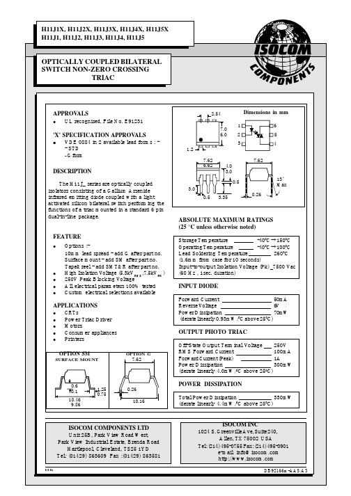
Normalised Repetitive Peak Off-state Voltage vs. Ambient Temperature
RMS on-state current I T (Arms)
0.1
0.05
Normalised to TA = 25°C
0 -30 0 25 50 75 100 125 Ambient temperature TA ( °C ) Forward Current vs. Ambient Temperature 80 70 Forward current I F (mA) 60 50 40 30 20 10 0 -30 0 25 50 75 100 125 Ambient temperature TA ( °C ) Normalised Input Trigger Current vs. Ambient Temperature 1.4 1.2 1.0 0.8 0.6 0.4 0.2 0 -30 0 25 50 75 100 Ambient temperature TA ( °C )
8/8/01
ISOCOM INC 1024 S. Greenville Ave, Suite 240, Allen, TX 75002 USA Tel: (214) 495-0755 Fax: (214) 495-0901 e-mail info@
DB92166m-AAS/A3
元器件交易网
ELECTRICAL CHARACTERISTICS ( TA = 25°C Unless otherwise noted ) PARAMETER Input Forward Voltage (VF) Reverse Current (IR) Peak Off-state Current ( IDRM ) Peak Blocking Voltage ( VDRM ) On-state Voltage ( VTM ) Critical rate of rise of off-state Voltage ( dv/dt ) ( note 1 ) Critical rate of rise of commutating Voltage ( dv/dt ) ( note 1 ) 250 1.5 10 0.1 0.2 3.0 MIN TYP MAX UNITS 1.2 1.5 100 100 V µA nA V V V/µs V/µs I load = 15mA, VIN = 30V ( fig 1. ) TEST CONDITION IF = 10mA VR = 6V VDRM = 250V (note 1 ) IDRM = 100nA ITM = 100mA ( peak )
DDR-CRS-RS2-1中文资料

18/08/05
DomiLED AlInGaP DDx-xRS - Catalogue-v4
Page 2 of 11
元器件交易网
DOMINANT Semiconductors
wavelength group is allowed for each reel. 5. An optional Vf binning is also available upon request. Binning scheme is as per following table.
18/08/05
Part Number DDA, DDS, DDR-CJS, DDR-SJS, DDG
DDH, DDO, DDY-CJS, DDY-SJS DDR-TJS, DDY-TJS
Vf @ If = 20mA
Typ. (V)
Max. (V)
2.1
2.3
Vr @ Ir = 100uA Min.(V) 12
2.2
DDR-CRS-QR2-1 • DDR-CRS-Q1 • DDR-CRS-Q2 • DDR-CRS-R1 • DDR-CRS-R2
** Not for new design.
AlInGaP Red, 625nm
DDR-CRS-RS2-1 • DDR-CRS-R1 • DDR-CRS-R2 • DDR-CRS-S1 • DDR-CRS-S2
X
615 – 621
DDO; Orange
Full
600 – 612
W
600 – 603
X
嵌入式工业计算机产品数据手册说明书
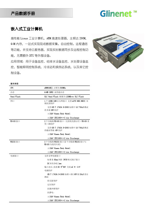
产品数据手册嵌入式工业计算机基本参数CPU ARM926EJ,主频为300MHz内存64MB DDR2高性能内存Nand Flash SLC Nand Flash 板载为128MByte SLC Flash 网口1个100M/10M 以太网接口支持AUTO MDI/MDIX 双级抗雷防护支持GB/T 17626.5-2008标准中10/700uS 测试的3级2KV 防护±15kV Human Body Model±15kV IEC1000-4-2Air DischargeRS485接口2个全隔离RS485接口(支持收发指示灯)RS485采用三级防护支持GB/T 17626.5-2008标准中10/700uS 测试的最高等级4KV 防护±15kV Human Body Model±15kV IEC1000-4-2Air DischargeRS232接口2个全隔离RS232接口(2个全隔离RS232接口与RS485为复用关系)±15kV Human Body Model±15kV IEC1000-4-2Air Discharge电源接口支持2种电源接口标准5.08mm 间距3PIN 欧式端子接口DC 座5.5*2.1mm输入电压:直流DC 9~36V 交流AC 9~24V电源防护GB/T 17626.5-2008标准4级(4KV)8/20uS 雷击测试防反接保护过压保护抗脉冲群保护抗静电:±15kV Human Body Model±15kV IEC1000-4-2Air Discharge高性能Linux 工业计算机,ARM 高速处理器,主频达200M,64M 内存,一站式实现现场数据采集、自动控制、远程通信等功能,并支持云服务器,实现实时数据同步及远程控制功能,无需额外DTU 等外围设备。
应用领域:用于设备监控,给排水设备监控,水处理设备监控,智能照明控制系统,冷冻站和换热站系统,以及其它控制设备。
金士顿+KVR1333D3D8R9S 4GHB+内存+说明书

KVR1333D3D8R9S/4GHB4GB 512M x 72-Bit PC3-10600CL9 Registered w/Parity 240-Pin DIMMDESCRIPTIONThis document describes ValueRAM’s 512M x 72-bit (4GB) DDR3-1333MHz CL9 SDRAM (Synchronous DRAM) regis-tered w/parity, dual-rank memory module, based on eighteen 256M x 8-bit DDR3-1333MHz FBGA components. The SPD is programmed to JEDEC standard latency 1333MHz timing of9-9-9 at 1.5V. This 240-pin DIMM uses gold contact fingers and requires +1.5V. The electrical and mechanical specifications are as follows:FEATURES• JEDEC standard 1.5V ± 0.075V Power Supply• VDDQ = 1.5V ± 0.075V• 667MHz fCK for 1333Mb/sec/pin• 8 independent internal bank• Programmable CAS Latency: 6,7,8,9,10• Programmable Additive Latency: 0, CL - 2, or CL - 1 clock • Programmable CAS Write Latency(CWL) = 7 (DDR3-1333)• 8-bit pre-fetch• Burst Length: 8 (Interleave without any limit, sequential with starting address “000” only), 4 with tCCD = 4 which does not allow seamless read or write [either on the fly using A12 or MRS]• Bi-directional Differential Data Strobe• Internal (self) calibration : Internal self calibration through ZQ pin (RZQ : 240 ohm ± 1%)• On Die Termination using ODT pin• On-DIMM thermal sensor (Grade B)• Average Refresh Period 7.8us at lower than TCASE 85°C, 3.9us at 85°C < TCASE ≤ 95°C• Asynchronous Reset• PCB : Height 1.180” (30.00mm), double sided componentDRAM Supported: Hynix B-DieSPECIFICATIONSCL(IDD) 9 cyclesRow Cycle Time (tRCmin) 49.5ns (min.)Refresh to Active/Refresh 160ns (min.)Command Time (tRFCmin)Row Active Time (tRASmin) 36ns (min.)Power 2.812 W (operating)UL Rating 94 V - 0Operating Temperature 0° C to 85° CStorage Temperature -55° C to +100° CContinued >>continued ValueRAM。
S1D13305中文资料
元器件交易网
The information of the product number change
Starting April 1, 2001, the product number will be changed as listed below. To order from April 1, 2001 please use the new product number. For further information, please contact Epson sales representative.
SDU1374#0C SDU1375#0C SDU1376#0C SDU1376BVR SDU1378#0C
• S1D1380x Series New No. Previous No.
SDU1386#0C
New No.
S5U13806P00C
S5U13503P00C S5U13504P00C S5U13505P00C S5U13506P00C
S1D13305 Series S1D13305D00A S1D13305F00A S1D13305F00B
S1D1370x Series S1D13704F00A S1D13705F00A S1D13706B00A S1D13706F00A S1D13708 Series
• S1D1350x Series Previous No.
S5U13704P00C S5U13705P00C S5U13706P00C S5U13706B32R S5U13708P00C
• S1D13A0x Series Previous No.
SDU13A3#0C SDU13A4#0C
New No.
2SJ352中文资料

2SJ352中⽂资料2SJ351, 2SJ352Silicon P-Channel MOS FETADE-208-1431st. EditionApplicationLow frequency power amplifierComplementary pair with 2SK2220, 2SK2221FeaturesHigh power gainExcellent frequency responseHigh speed switchingWide area of safe operationEnhancement-modeGood complementary characteristicsEquipped with gate protection diodesOrdering InformationType No.VDSX2SJ351–180 V2SJ352–200 V2SJ351, 2SJ3522OutlineAbsolute Maximum Ratings (Ta = 25°C)ItemSymbol Ratings Unit Drain to source voltage 2SJ351V DSX–180V2SJ352–200Gate to source voltage V GSS ±20V Drain currentI D –8A Body to drain diode reverse drain current I DR –8A Channel dissipation Pch*1100W Channel temperature Tch 150°C Storage temperature Tstg –55 to +150°C Note:1.Value at T C = 25°C2SJ351, 2SJ3523Electrical Characteristics (Ta = 25°C)ItemSymbol Min Typ Max Unit Test conditions Drain to source 2SJ351V (BR)DSX–180——VI D = –10 mA, V GS = 10 Vbreakdown voltage2SJ352–200——Gate to source breakdown voltageV (BR)GSS ±20——V I G = ±100 µA, V DS = 0Gate to source cutoff voltage V GS(off)–0.15—–1.45V I D = –100 mA, V DS =–10 V Drain to source saturation voltageV DS(sat)——–12V I D = –8 A, V GD = 0*1Forward transfer admittance |y fs |0.7 1.0 1.4S I D = –3 A, V DS = –10 V*1Input capacitance Ciss —800—pF V GS = 5 V, V DS = –10 V,Output capacitanceCoss —1000—pF f = 1 MHzReverse transfer capacitance Crss —18—pF Turn-on time t on —320—ns V DD = –30 V, I D = –4 A Turn-off time t off—120—nsNote:1.Pulse test2SJ351, 2SJ35242SJ351, 2SJ3526Hitachi CodeJEDECEIAJWeight (reference value)TO-3P—Conforms5.0 gUnit: mmCautions1.Hitachi neither warrants nor grants licenses of any rights of Hitachi’s or any third party’s patent,copyright, trademark, or other intellectual property rights for information contained in this document.Hitachi bears no responsibility for problems that may arise with third party’s rights, includingintellectual property rights, in connection with use of the information contained in this document.2.Products and product specifications may be subject to change without notice. Confirm that you have received the latest product standards or specifications before final design, purchase or use.3.Hitachi makes every attempt to ensure that its products are of high quality and reliability. However,contact Hitachi’s sales office before using the product in an application that demands especially high quality and reliability or where its failure or malfunction may directly threaten human life or cause risk of bodily injury, such as aerospace, aeronautics, nuclear power, combustion control, transportation,traffic, safety equipment or medical equipment for life support.4.Design your application so that the product is used within the ranges guaranteed by Hitachi particularly for maximum rating, operating supply voltage range, heat radiation characteristics, installationconditions and other characteristics. Hitachi bears no responsibility for failure or damage when used beyond the guaranteed ranges. Even within the guaranteed ranges, consider normally foreseeable failure rates or failure modes in semiconductor devices and employ systemic measures such as fail-safes, so that the equipment incorporating Hitachi product does not cause bodily injury, fire or other consequential damage due to operation of the Hitachi product.5.This product is not designed to be radiation resistant.6.No one is permitted to reproduce or duplicate, in any form, the whole or part of this document without written approval from Hitachi.7.Contact Hitachi’s sales office for any questions regarding this document or Hitachi semiconductor products.Hitachi, Ltd.Semiconductor & Integrated Circuits.Nippon Bldg., 2-6-2, Ohte-machi, Chiyoda-ku, Tokyo 100-0004, Japan Tel: Tokyo (03) 3270-2111 Fax: (03) 3270-5109 Copyright ' Hitachi, Ltd., 1999. All rights reserved. Printed in Japan.Hitachi Asia Pte. Ltd.16 Collyer Quay #20-00Hitachi TowerSingapore 049318Tel: 535-2100Fax: 535-1533URLNorthAmerica : http:/doc/bfe7be20915f804d2b16c12b.html /Europe :/doc/bfe7be20915f804d2b16c12b.html /hel/ecg Asia (Singapore):/doc/bfe7be20915f804d2b16c12b.html .sg/grp3/sicd/index.htm Asia (Taiwan):/doc/bfe7be20915f804d2b16c12b.html /E/Product/SICD_Frame.htm Asia (HongKong):/doc/bfe7be20915f804d2b16c12b.html /eng/bo/grp3/index.htm Japan :http://www.hitachi.co.jp/Sicd/indx.htmHitachi Asia Ltd.Taipei Branch Office3F, Hung Kuo Building. No.167, Tun-Hwa North Road, Taipei (105)Tel: <886> (2) 2718-3666Fax: <886> (2) 2718-8180 Hitachi Asia (Hong Kong) Ltd.Group III (Electronic Components)7/F., North Tower, World Finance Centre,Harbour City, Canton Road, Tsim Sha Tsui,Kowloon, Hong Kong Tel: <852> (2) 735 9218Fax: <852> (2) 730 0281 Telex: 40815 HITEC HXHitachi Europe Ltd.Electronic Components Group.Whitebrook ParkLower Cookham Road MaidenheadBerkshire SL6 8YA, United Kingdom Tel: <44> (1628) 585000Fax: <44> (1628) 778322Hitachi Europe GmbHElectronic components Group Dornacher Stra§e 3D-85622 Feldkirchen, Munich GermanyTel: <49> (89) 9 9180-0Fax: <49> (89) 9 29 30 00Hitachi Semiconductor (America) Inc.179 East Tasman Drive,San Jose,CA 95134 Tel: <1> (408) 433-1990Fax: <1>(408) 433-0223For further information write to:。
6Cxxxx-xxx-4GS中文资料

6C SeriesSPECIFICATIONS STANDARD *SPECIAL ELECTRICALCenter Frequency (Fc)3000 to 6000 Mhz 2000 to 9000 MHz 3dB Relative Bandwidth (% of FC) 1 to 2.00.5 to 2.5Number of Sections Available 3 to 6 2 to 7Nominal Impedance 50 Ohms 50 Ohms Maximum Insertion Loss See below See below Maximum VSWR 1.5/1 1.3/1Attenuation in the StopbandSee Graph See Graph Maximum Input Power (Average)(Watts to 10,000 ft.)25% of PEAK See StandardMaximum Input Power (Peak)(Watts to 10,000 ft.)1500 x 3dB BW (MHz)Fc (MHz)See StandardENVIRONMENTAL Shock 15 G's 25 G's Vibration 10 G's 20 G's Humidity90% relative100% relativeAltitude Unlimited UnlimitedTemperature Range (Operating)0 to + 50 degreescelsius-20 to + 70 degreescelsiusTemperature Range (Non-Operating)-25 to + 70 degreescelsius-40 to +85 degreescelsiusMECHANICALApproximate Weight in oz.0.9 x H x L0.8 x H x L Mounting Provisions See below See belowSpecial Configurations Consult Factory Consult FactoryLOSS FACTOR FOR ALL 6C SERIES FILTERS ISLF=0.4Note: Lower loss designs are available with thisseries. Consult Application Engineering.MECHANICAL SPECIFICATIONSL DIMENSION = 0.7 x (NO. OF SECTIONS) + 0.37 inch APPROX.W DIMENSION = 3000/(CENTER FREQ. MHz) + .75 inch APPROX.Connectors Available on 6C Series:Lark Code Type C DIM.Inches & MM Lark Code Type C DIM.Inches & MM A SMA JACK .375 & 9.5G N JACK .736 & 18.7BSMA PLUG.507 & 12.9H N PLUG .819 & 20.8.SSPECIALLark Engineering 6C SERIES元器件交易网The size shown is a standard used by Lark to facilitate a low cost, easily reproducible unit. Should you require another size, please submit all of your requirements-both electrical and mechanical. This will enable Lark Engineering to quote theoptimum design for your application.Lark Engineering 6C SERIES元器件交易网STOPBAND ATTENUATIONThe graphs on the following page define the normal specification limits on attenuation Lark bandpass filter series 2C, 3C, 4C, 5C, and 6C. The minimum level of attenuation in dB is shown as a "number of 3dB bandwidths fromcenter frequency".The exact relationship is as follows:1. 3dB Bandwidths From Center Frequency= Rejection Frequency (Mhz) -Center Frequency (Mhz) divided by 3dB Bandwidth (Mhz)Example:Given:2. Center Frequency = 600 MHzMinimum 3dB Bandwidth = 6 MHzNumber of Sections = 5Find: Minimum attenuation levels at 588 MHz and 610 MHz.3dB BW's from Fc = 588 - 600 / 6 = - 2.0and 610 - 600 / 6 = + 1.6The answer can be read directly from the graph. Using the 5 section curve at the point -2.0 (588 MHz) we find the minimum level of attenuation is 62dB. At +1.6 (610 MHz) the minimum level of attenuation is 51dB.For special requirements, please contact our Application EngineeringDepartment.STOPBAND ATTENUATION。
HS1J中文资料

- 300 -
元器件交易网
RATINGS AND CHARACTERISTIC CURVES (HS1A THRU HS1M)
FIG.1- REVERSE RECOVERY TIME CHARACTERISTIC AND TEST CIRCUIT DIAGRAM
trr +0.5A (-) DUT (+) 50Vdc (approx) (-) PULSE GENERATOR (NOTE 2) 1W NON INDUCTIVE OSCILLOSCOPE (NOTE 1) (+) 0 -0.25A
HS
1.4
Tj=25 0C
1J
-H
10
1
S1
1.6 FORWARD VOLTAGE. (V)
FIG.5- MAXIMUM NON-REPETITIVE FORWARD SURGE CURRENT
40 70
FIG.6- TYPICAL JUNCTION CAPACITANCE
PEAK FORWARD SURGE CURRENT. (A)
.056(1.41) .035(0.90) .210(5.33) .195(4.95)
.012(.31) .006(.15) .008(.20) .004(.10)
Dimensions in inches and (millimeters)
Maximum Ratings and Electrical Characteristics
HS 1F
HS 1G
HS 1J
HS 1K
HS 1M
Units V V V A A
VRRM VRMS VDC I(AV) IFSM VF IR Trr Cj RθJA
爱立信GJS系列电对流产品说明说明书

Eaton GJS3125AAMEaton Series G molded case circuit breaker, JG-frame, GJ, Adjustable thermal, adjustable magnetic trip, Three-pole, 125A, 600 Vac, 85 kAIC at 240 Vac, 40 kAIC at 415 Vac, 35 kAIC at 480 Vac, 18 kAIC at 600 Vac, Line/load end caps, MetricGeneral specificationsEaton Series G complete molded case circuit breakerGJS3125AAM 7821169013713.57 in4.13 in 4.13 in 12 lb Eaton Selling Policy 25-000, one (1) year from the date of installation of the Product or eighteen (18) months from the date of shipment of the Product, whichever occurs first.IEC Rated Product NameCatalog Number UPCProduct Length/Depth Product Height Product Width Product Weight WarrantyCertificationsMetric40 kAIC at 415 Vac85 kAIC at 240 Vac35 kAIC at 480 Vac18 kAIC at 600 VacJGGJComplete breakerLine and load end caps600 Vac125 AAdjustable thermal, adjustable magnetic Three-pole Application of Multi-Wire Terminals for Molded Case Circuit Breakers Application of Tap Rules to Molded Case Breaker TerminalsStrandAble terminals product aidPower metering and monitoring with Modbus RTU product aidMotor protection circuit breakers product aidMolded case circuit breakers providing higher levels of selective coordination product aidComprehensive circuit protection for control panel applicationsCircuit breaker motor operators product aidHigh performance operating handles for Series G circuit breakers product aidMulti-wire lugs product aidCurrent limiting molded case circuit breaker module product aid Current limiting molded case circuit breaker module for series G, JG and CLSeries G MCCB quick selectorPlug-in adapters for molded case circuit breakers product aidBreaker service centersMolded case circuit breakers catalogEaton's Volume 4—Circuit ProtectionSeries G GJ-Frame Molded Case Circuit Breaker - InstructionsMOEM MCCB product selection guideEaton Specification Sheet - GJS3125AAMNG and ND-Frame molded case circuit breakersMounting hardware Interrupt ratingFrameCircuit breaker type Circuit breaker frame type TerminalsVoltage rating Amperage RatingTrip TypeNumber of poles Application notesBrochuresCatalogsInstallation instructions Specifications and datasheetsEaton Corporation plc Eaton House30 Pembroke Road Dublin 4, Ireland © 2023 Eaton. All Rights Reserved. Eaton is a registered trademark.All other trademarks areproperty of their respectiveowners./socialmedia。
Z1桩柱钢筋构造(表格绘制)

绘制模板图形中的表格:用word表达,自动转换成dxf中的表格,参与排图或插入到已有的图块中/*模板制作使用说明:1.表格标题的输入:标题标题说明2.行不绘制:3.列不绘制:!%!4.单元的格式输入:TH(1-3)文字样式,:1表正;2表头;3表头单位//为马波处的规定TE(1-17)单元类型,TA(1-9)对齐样式,TW(0-2)无效单元格式DR(Val)行高,DC(Val)列宽放在{}中,每个以英文逗号","隔开,如{TH1,TE3}以前表格的输入需要用||和&&,模板中不能用,此时用\t来代替||,用\n来代替&&5.在模板中特殊符号的输入:格式为:%%大写英文%%A:CStringm_SupOn;//上标开启%%B:CStringm_SupOff;//上标关闭%%C:CStringm_SubOn;//下标开启%%D:CStringm_SubOff;//下标关闭%%E:CStringm_GJI;//!一级//其中m_GJI对应的材料库中[A1]筋的特殊字符%%F:CStringm_GJII;//!二级//其中m_GJI对应的材料库中[A2]筋的特殊字符%%G:CStringm_GJIII;//!三级//其中m_GJI对应的材料库中[A3]筋的特殊字符%%H:CStringm_GJIV;//!四级//其中m_GJI对应的材料库中[A4]筋的特殊字符%%I:CStringm_GJIV2;//!四级KL400%%J:CStringm_TendonH;//!纵向钢束//对应的材料库中[B1]筋的特殊字符%%K:CStringm_TendonV;//!竖向钢束//对应的材料库中[B2]筋的特殊字符%%L:CStringm_GSPre;//!钢束前缀Ф6.自定义缺省的单元格格式:放在表格标题中,放在表格标题中单元格式是本表格的缺省单元格式,如标题标题说明{TH1,TE3} */桩柱一起材料数量表(明细+单个汇总)Startloop[PROP(@FName@).DTSN]墩柱材料数量表●柱材料数量表(明细+单个汇总)Startloop[PROP(@FName@).DTSN]墩柱材料数量表●桩材料数量表(明细+单个汇总)Startloop[PROP(@FName@).DTSN]桩基材料数量表●全桥柱材料汇总表●●●●●。
二极管S1J

06-Sep-051 2Document Number 8871106-Sep-05S1A thru S1MVishay General SemiconductorElectrical Characteristics(T A = 25°C unless otherwise noted)Thermal Characteristics(T A = 25°C unless otherwise noted)Notes:(1) Thermal resistance from junction to ambient and from junction to lead mounted on P.C.B.with 0.2 x 0.2" (5.0 x 5.0 mm) copper pad areasRatings and Characteristics Curves(T A = 25 °C unless otherwise noted)ParameterTest condition SymbolS1AS1BS1DS1GS1JS1KS1MUnitMaximum instantaneous forward voltageat 1.0 AV F 1.1 V Maximum DC reverse current at Rated DC blocking voltage T A = 25 °C T A = 125 °CI R1.05.0µA50Typical reverse recovery time at I F = 0.5 A, I R = 1.0 A, I rr = 0.25 A t rr 1.8 µsTypical junction capacitanceat 4.0 V , 1 MHzC J 12 pFParameterSymbolS1AS1BS1DS1GS1JS1KS1MUnit Typical thermal resistance (1) R θJA 75 85°C/WR θJL 2730Figure 1. Forward Current Derating Curve Figure 2. Maximum Non-Repetitive Peak Forward Surge CurrentS1A thru S1MDocument Number 8871106-Sep-05Vishay General Semiconductor3Package outline dimensions in inches (millimeters)Figure 3. Typical Instantaneous Forward Characteristics Figure 4. Typical Reverse Leakage CharacteristicsFigure 5. Typical Junction CapacitanceFigure 6. Typical Transient Thermal ImpedanceLegal Disclaimer NoticeVishay Document Number: Revision: 08-Apr-051NoticeSpecifications of the products displayed herein are subject to change without notice. Vishay Intertechnology, Inc., or anyone on its behalf, assumes no responsibility or liability for any errors or inaccuracies.Information contained herein is intended to provide a product description only. No license, express or implied, by estoppel or otherwise, to any intellectual property rights is granted by this document. Except as provided in Vishay's terms and conditions of sale for such products, Vishay assumes no liability whatsoever, and disclaims any express or implied warranty, relating to sale and/or use of Vishay products including liability or warranties relating to fitness for a particular purpose, merchantability, or infringement of any patent, copyright, or other intellectual property right. The products shown herein are not designed for use in medical, life-saving, or life-sustaining applications. Customers using or selling these products for use in such applications do so at their own risk and agree to fully indemnify Vishay for any damages resulting from such improper use or sale.。
- 1、下载文档前请自行甄别文档内容的完整性,平台不提供额外的编辑、内容补充、找答案等附加服务。
- 2、"仅部分预览"的文档,不可在线预览部分如存在完整性等问题,可反馈申请退款(可完整预览的文档不适用该条件!)。
- 3、如文档侵犯您的权益,请联系客服反馈,我们会尽快为您处理(人工客服工作时间:9:00-18:30)。
• Low current surface mount LED. • 120° viewing angle.
• Small package outline (LxWxH) of 3.2 x 2.8 x 1.8 mm. • Qualified according to JEDEC moisture sensitivity Level 2. • Compatible to both IR reflow soldering and TTW soldering.
Part Ordering Number Chip Technology /
Color Luminous Intensity @ If = 10mA Iv ( mcd )
DDR-GJS-J2L1-1-I1
• DDR-GJS-J2
• DDR-GJS-K1
• DDR-GJS-K2
• DDR-GJS-L1GaP /
Red, 625 nm
5.6 … 14.0
5.6 … 7.2
7.2 … 9.0
9.0 … 11.2
11.2 … 14.0
DDO-GJS-H2K1-1-I1
• DDO-GJS-H2
• DDO-GJS-J1
• DDO-GJS-J2
• DDO-GJS-K1GaP /
Orange, 605 nm
3.55 … 9.0
3.55 …
4.5
4.5 …
5.6
5.6 … 7.2
7.2 … 9.0
DDY-GJS- H2K1-1-I1
• DDY-GJS-H2
• DDY-GJS-J1
• DDY-GJS-J2
• DDY-GJS-K1GaP /
Yellow, 587 nm
3.55 … 9.0
3.55 …
4.5
4.5 …
5.6
5.6 … 7.2
7.2 … 9.0
DDG-GJS- KL2-1-I1
• DDG-GJS-K1
• DDG-GJS-K2
• DDG-GJS-L1
• DDG-GJS-L2GaP /
Green, 570 nm
7.2 … 18.0
7.2 … 9.0
9.0 … 11.2
11.2 … 14.0
14.0 … 18.0
DDP-GJS-GH2-1-I1
• DDP-GJS-G1
• DDP-GJS-G2
• DDP-GJS-H1
• DDP-GJS-H2GaP /
Green, 560 nm
1.80 … 4.50
1.80 …
2.24
2.24 … 2.80
2.80 …
3.55
3.55 …
4.50
NOTE:
1. All part number above comes in a quantity of 2000 units per reel.
2. Luminous intensity is measured with an accuracy of ±11%.
3. Wavelength binning is carried for all units as per the wavelength-binning table. Only one
wavelength group is allowed for each reel.
Characteristics.
Forward voltage @ If=10 mA. Chip Type Viewing angle
at 50% Iv
Max reverse current, I R
@ V R = 5V.
2.05 V (typ.); 2.45 V (max) GaP 120° 100 μA
All forward voltages are measured using a current pulse of 1 ms and has an accuracy of ±0.1 V. Wavelength Grouping.
Color Group Wavelength distribution (nm) DDR; Red Full 620 – 635
DDO; Orange Full
W
X
Y
Z 600 – 612
600 - 603
603 - 606
606 - 609
609 - 612
DDY; Yellow Full
W
X
Y
Z 582 – 594 582 – 585 585 – 588 588 - 591 591 - 594
DDG; Green Full
W
X
Y
Z 564.5 – 576.5 564.5 – 567.5 567.5 – 570.5 570.5 – 573.5 573.5 – 576.5
DDP; Pure Green Full
W
X
Y
Z 552.5 – 564.5 552.5 – 555.5 555.5 – 558.5 558.5 – 561.5 561.5 – 564.5
Dominant wavelength is measured with an accuracy of ±1 nm.
Absolute Maximum Ratings.
Maximum Value Unit DC forward current. 30 mA Peak pulse current; (tp ≤ 10 μs, Duty cycle = 0.005) 500 mA Reverse voltage. 5 V LED junction temperature. 100 °C Operating temperature. -40 … +100 °C Storage temperature. -40 … +100 °C Power dissipation ( at room temperature ) 75 mW
Recommended Solder Pad
Relative luminous intensity vs. forward current. Forward current vs. forward voltage.
Taping And Orientation.Reels come in quantity of 2000 units.
Reel diameter is 180 mm .
Recommended Sn-Pb IR-Reflow Soldering Profile.
Recommended Pb Free IR-Reflow Soldering Profile.
NOTE.
All the information published is considered to be reliable. However, DOMINANT Semiconductors does not assume any liability arising out of the application or use of any product described herein.
DOMINANT Semiconductors reserves the right to make changes at any time without notice to any products in order to improve reliability, function or design.
DOMINANT Semiconductors products are not authorized for use as critical components in life support devices or systems without the express written approval from the managing director of DOMINANT Semiconductors.。