system-level ESD
ESD系统技术说明书

1.1 范围.......................................................................................................................................................4 1.2 系统方案.............................................................................................................................................. 4 1.3 报价书的要求...................................................................................................................................... 4
SIS与ESD的区别
个人认为他们的区别应该不是很大Esd(EmergencyShutdownDevice):紧急停车系统,多数应用于石油和化工系统,是一个独立于DCS系统的控制单元,在工艺发生危险状况时,对设备,环境等进行紧急的启挺,开关操作。
配置设备以高档的PLC居多,多数处理DI/DO点,现在多数与DCS进行通讯。
SIS(SIS,safetyinstrumented system):安全仪表系统,主要用于汽轮机,压缩机等高速运转设备,对轴承的转速,震动,位移,温度等进行检测,对设备进行保护,原来设计多为模块组合,相当于与智能仪表的组合体。
SIS是安全仪表系统,ESD是紧急停车系统,ESD属于SIS的一部分。
SIS包括现场仪表、逻辑解决器、执行机构三部分,这三个部分都要是安全设计的,常规的ESD系统只是SIS的逻辑解决器这部分,当然也要是安全设计的。
随便举个例子,不一定合适,但是可以帮助理解这些概念。
西门子的PCS7 系统。
包含了S7-400H硬件,WinCC监控软件,Simaticnet 通讯软件。
Step7编程软件。
PDM等智能仪表工具。
PCS7是一系列软件,硬件的组合体,是一个系统的概念。
SIS基本上也是同样的道理。
从本质上来讲,SIS的硬件系统不光包括,SIS控制器及IO(例如Triconex,HIMA,西门子400FH)。
还应包括所有跟控制器接口的其他输入部件,例如获得TUVSIL认证的传感器,变送器,检测装置;还应该包括所有输出部件,如获得TUV SIL认证的执行器(液压安全执行器,气动安全执行器,电动型安全执行器),还应该有获得认证的现场设备。
--要求严格的现场,阀门本体也必须是有TUV 证书的。
例如核电厂的安全阀不光是锅炉与压力容器质检合格,还应该有核检证书,还应该有TUV的安规证书,明确标明是SIL几等级。
那么,我们现在再来理解这些概念,,, 安全型控制器(目前这个叫法最科学)仅仅是SIS系统硬件中的一环。
ESD静电控制手册(ESD手册中英文)

ESD静电控制手册TABLE OF CONTENTS1. Purpose 目的2. Scope 范围3. Definition 定义4. Responsibility 职责5. Operation Content 作业内容5.1 ESD Control Program ESD 管制方案5.2 ESD Control Program Mgr or Coordinator ESD 管制方案经理或协调员5.3 Update 文件修改与更新5.4 ESD Control Operation ESD 管制作业5.4.1 ESD Protected Area ESD 保护区5.4.2 Training Requirement 培训要求5.4.3 ESD Test requirements ESD 测试要求5.4.4 ESD Grounding System ESD 接地系统5.4.5 ESD Floor Control ESD 地板管制5.4.6 ESD Garment & ESD Cap Control 静电衣服&静电帽管制5.4.7 ESD Shoe Control 静电鞋管制5.4.8 ESD Gloves& Finger Cots Control 静电手套&指套管制5.4.9 ESD wrist strap Control 静电手环管制5.4.10 Equipment ESD Control 设备ESD 管制5.4.11 Fixture& Tools Control 工治具管制5.4.12 Work Surface control 工作台管制5.4.13 ESD Marking ESD 标示5.4.14 ESD Packaging Material ESD 包装材料管制5.4.15 ESD Seating 静电座椅5.4.16 Soldering Iron Control 铬铁静电管制5.4.17 Air Ionizer Control 离子风机管制5.5 Sub-contractor control 外包商管制6.Reference 参考文件ESD Manual 静电控制手册1. Purpose 目的To prevent ESDS objects in manufacture, assembly, install, package, test, inspection,preservation, transport or other operation activities from damage, and protect electrical or electronic parts, assemblies and equipment so as to guarantee the product quality, so ESD protection.为防止静电敏感元器件在生产、组装,安装,包装,测试,检验、保存、運送及其他活动中受到静电之损害,保护电子器件,组件和设备,从而保证产品品质,特制订此手册,以提供本公司静电防护之最高指引.2. Scope 范围Applicable to all the related activities from ESD objects in DXC适用于公司所有ESD 敏感物件之相关活动作业3. Definition 定义3.1 ESD-E lectro S tatic D ischarge, the transfer or movement of charge between objects that are at different electrical potentials by direct contact or induced by electrostatic field.ESD-静电释放,是指通过直接接触或静电场感应的方式,在不同电势差物体间的电荷转移或移动。
静电保护的重要性
深入探討靜電保護的重要性作者:星曜半導體(V ALORSTAR S EMICONDUCTOR)行銷副總林居敬今日終端產品廠商均面臨到增加產品特性、減少產品尺寸的趨勢;當產品具備更多功能時,相對I/O port隨之增多,導致靜電更易干擾系統或是損壞IC。
此外,隨著市場上消費性電子和可攜式產品體積越做越小,對於主板面積的要求亦日趨小型化及高密度。
半導體元件的發展也隨之變化,以小型化、高密度、功能複雜為其藍圖。
CMOS IC製程為增加其速度、整合度、及單位成本,元件尺寸越做越小。
雖經濟效益提高但也伴隨著信賴度的問題。
由於利用先進製程技術製造的IC電路內氧化層比較薄,閘極(Gate)氧化層更易受到損害。
在深次微米互補式金氧半導體(CMOS)製程,因為閘極氧化層的低崩潰電壓,且閘極氧化層的崩潰電壓和PN Junction 的崩潰電壓的差值愈來愈小,使得靜電保護電路的驅動電壓範圍也隨之愈來愈小,且因為元件尺寸變的更小,對於靜電護能力下降,大大增加失效的機率。
這也是為什麼近來年靜電問題越來越受到重視;ESD保護對高密度、小型化和複雜功能的電子設備來說具有重要意義。
何謂ESD?其種類為何?ESD是Electrostatic Discharge的縮寫,即靜電放電;ESD對電子產品的傷害一直是不易解決的問題。
一般受到ESD作用時會出現不穩定的狀況,輕微只需重開機即可;嚴重可能導致電子產品內的電子元件毀損。
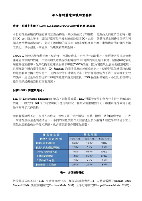
而且靜電無所不在,多是人為造成,例如:電子元件製造、組裝、搬運、儲存(請參考表一)。
表一描述在幾個生產製造環境下,不同的個體及動作大致會產生多少靜電;在乾燥的環境下加上空氣的流動造成分子互相摩擦,也會導致靜電作用更加顯著。
表一各環境靜電值依放電模式的不同,ESD又通常可以分為三種模式(請參考表二):人體放電模式(Human Body Mode,HBM)、機器放電模式(Machine Mode,MM)、元件充電模式(Charged Device Mode,CDM)。
ADUM3201ARZ中文资料
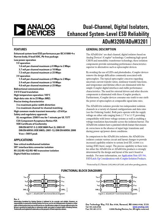
6 VOB
GND1 4
5 GND2
Figure 1. ADuM3200 Functional Block Diagram
Rev. 0
Information furnished by Analog Devices is believed to be accurate and reliable. However, no responsibility is assumed by Analog Devices for its use, nor for any infringements of patents or other rights of third parties that may result from its use. Specifications subject to change without notice. No license is granted by implication or otherwise under any patent or patent rights of Analog Devices. Trademarks and registered trademarks are the property of their respective owners.
5 V operation 1.6 mA per channel maximum @ 0 Mbps to 2 Mbps 3.7 mA per channel maximum @ 10 Mbps 7.5 mA per channel maximum @ 25 Mbps
3 V operation 1.4 mA per channel maximum @ 0 Mbps to 2 Mbps 2.4 mA per channel maximum @ 10 Mbps 4.6 mA per channel maximum @ 25 Mbps
ESD LU综述
Model Parameters : C=200 pF, R= 0 Ohms (机器等效电阻和电容) ESD Tester parasitics : L~2.5 uH, R=10 Ohms , Ct=20…95 pF。Cs= ~1..3 pF
CMM = 200pF, RMM = 0 ohm IPeak = ~3.8A (for MM 200V) ~6-8ns rise time, ~63ns period
2
Copyright © ABC Inc. All rights reserved.
半导体失效原因
Failure Rate
6%
16%
7% 61%
4% 3% 3%
Internal Use
EOS/ESD Electrical testing Oxide/passivation fail Die fracture Lead short/open Wire bonds Others
R
C
8
Model Parameters : C=100 pF, R=1.5 kOhms(人体等效电阻和电容) ESD Tester parasitics : L~5-12 uH, Ct ~20-95 pF, Cs ~1-3 pF Ipeak = ~1.3A (for HBM 2000V) 10ns rise time, ~200ns pulse
此种模式的放电时间更短,仅约几毫微秒之内, 而且放电现象更难以真实的被模拟。因为IC内部 累积的静电会因IC组件本身对地的等效电容而变, IC摆放的角度与位置以及IC所用的包装型式都会 造成不同的等效电容。由于具有多项变化因素难 定,因此,有关此模式放电的工业测试标准为 (ESD DSP5.3.2)。组件充电放电模式的等效电路 图显示如左图所示
ESD模型和测试标准

1、ESD模型分类
2、HBM和MM测试方法标准
3、 CDM模型和测试方法标准
4、 EIC模型和测试方法标准
5、 TLP及其测试方法
6、拴锁测试
7、 I-V测试
8、标准介绍
1、ESD模型分类
因ESD产生的原因及其对集成电路放电的方式不同
,经过统计,ESD放电模型分下列四类:
(1) 人体放电模式 (Human-ቤተ መጻሕፍቲ ባይዱody Model, HBM)
(2) 机器放电模式 (Machine Model, MM)
(3) 组件充电模式 (Charged-Device Model, CDM)
(4) 电场感应模式 (Field-Induced Model, FIM)
另外还有两个测试模型:
(5)对于系统级产品测试的IEC电子枪空气放电模式
(6)对于研究设计用的TLP模型
引脚,将其作为参考节点连接到B端。其他
所有引脚依次连接到A端,并且在AB间接
入短接线。使用正负1000V的脉冲电压在
AB端,观察波形,经过所有引脚对的电流
波形必须符合如图波形
2、HBM和MM测试方法标准
HBM测试方法及标准
1.ANSI-STM5.1-2001
JESD22-A114D -2005
(2)ESD敏感度(sensitivity):引起器件失效的ESD等
级(level)
(3)ESD耐受电压(withstand voltage):在不引起器
件失效前提下的最大ESD等级
(4)步进耐压增强(Step stress test hardening):在步
进增加的测试电压下,器件的耐受电压的现象
4、 EIC模型和测试方法标准
技术管理(ESD静电放电知识讲座)

平南信华静电防护组
第三章:ESD控制国际标准
●项目管理具体技术方案简要介绍
接地 工作台 腕带系统 鞋类 地板 椅子 环境系统离子化
非环境系统离子 化 货架 移动设备 连续监测设备 服装
平南信华静电防护组
第三章:ESD控制国际标准 4. ESDA国际专家建议最佳的ESD控制措施为: ●人体静电电压控制在100V以内。 ●所有设备必须良好接地。
35
●所有产品上的静电电压控制在50V以内。
平南信华静电防护组
第三章:ESD控制国际标准
探讨问题:防静电地与设备地之间的关系问题?
平南信华静电防护组
第三章:ESD控制国际标准
37
探讨问题:防静电地与设备地之间关系问题,为什么?
●其次如果处于等电势下即使漏电人体也是安全的。
安全
平南信华静电防护组
第四章:ESD标识
平南信华静电防护组
第三章:ESD控制国际标准
●本标准静电控制领域指:超过或等于100V的人体模型器件活动; 如果低于100V时应有额外控制手段。
●静电放电的发生: i. 一个带电物体接近、接触静电放电敏感器件 ii. 当一个静电放电敏感器件暴露在一个静电场中的时候,将它接 地。
●ESD管理方案:
• • • • • • • 培训 认证检验 接地及等电位相连系统 人员接地 静电放电保护区之要求 包装系统 标记
平南信华静电防护组
10
第一章:静电的自然现象、产生原理及危害性
4.静电产生的方式: ●摩擦起电 ●传导起电 ●感应带电 例子:CPM对金属尺子传导静电 例子:CPM给金属尺子充放电
平南信华静电防护组
第一章:静电的自然现象、产生原理及危害性
摩擦起电
ESD
ESD测试标准的差异 测试标准的差异
SYSTEM LEVEL 系统级产品采用 IEC61000-4-2测试标准 - - 测试标准 COMPONET LEVEL 元件级产品采 用MIL-STD-883E测试标准 - - 测试标准 因为测试标准的不同, 因为测试标准的不同,线路中被保护或 设计保护线路目标的元件,(一般为IC ,(一般为 设计保护线路目标的元件,(一般为 晶片)其可承受的ESD KV级别与系统 晶片)其可承受的 级别与系统 ESD之KV级别有完全不同的含义 之 级别有完全不同的含义
IC ESD保护线路设计参考 保护线路设计参考
Whole-Chip ESD Protection Scheme with ESD Buses II ESD-Bus-1 ESD Clamp ESD ESD ESD Cell Cell Cell VDD1 PowerRail ESD Clamp Circuit Circuit I VSS1 ESD-Bus-2 ESD Cell ESD Cell VSS6 PowerRail ESD Clamp Circuit Circuit VI VDD6 ESD-Bus-3 ESD Cell VDD2 Circuit II VSS2 ESD Cell ESD Cell VSS5 Circuit V VDD5 ESD Cell VDD3 Circuit III VSS3 ESD Cell ESD Cell VSS4 Circuit IV VDD4 ESD Cell ESD-Bus-4 ESD Clamp
ESD Clamp
ESD Cell 以2组二 组二 极管串联组合, 极管串联组合,再 反向并联的模组所 构成 ESD Clamp元件提 元件提 供真正的保护; 供真正的保护; ESD保护必须考虑 保护必须考虑 到个别线路的电源 系统以及所有线路 系统间的保护
安全仪表系统(ESD)
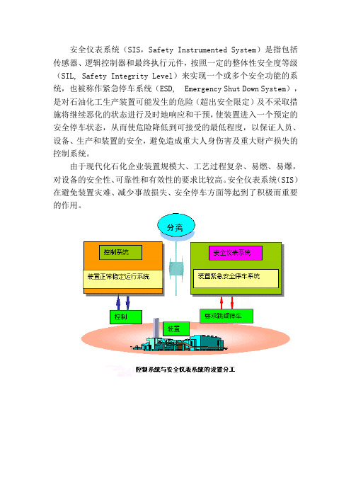
安全仪表系统(SIS,Safety Instrumented System)是指包括传感器、逻辑控制器和最终执行元件,按照一定的整体性安全度等级(SIL, Safety Integrity Level)来实现一个或多个安全功能的系统,也被称作紧急停车系统(ESD, Emergency Shut Down System),是对石油化工生产装置可能发生的危险(超出安全限定)及不采取措施将继续恶化的状态进行及时地响应和干预,使装置进入一个预定的安全停车状态,从而使危险降低到可接受的最低程度,以保证人员、设备、生产和装置的安全,避免造成重大人身伤害及重大财产损失的控制系统。
由于现代化石化企业装置规模大、工艺过程复杂、易燃、易爆,对设备的安全性、可靠性和有效性的要求比较高。
安全仪表系统(SIS)在避免装置灾难、减少事故损失、安全停车方面等起到了积极而重要的作用。
ADUM3100ARZ中文资料

3/06—Rev. 0 to Rev. A Updated Format..................................................................Universal Changes to Product Title, Features, General Description, and Note 1.......................................................................................... 1 Changes to Table 1............................................................................ 3 Changes to Table 2............................................................................ 4 Changes to Table 3............................................................................ 5 Added System-Level ESD Considerations and Enhancements Section................................................................... 13 Added Power Consumption Section............................................ 15
ESD
紧急停车系统1、名称、作用、构成2、相关标准及认证机构3、ESD和DCS的比较4、ESD设计应遵循的原则5、故障安全原则6、隐故障和显故障7、安全性及响应失效率8、可用性及可用度9、冗余和容错10、冗余逻辑的表决方法及其与安全性、可用性的关系11、普通PLC和安全PLC的区别12、取得TÜV认证的ESD产品13、工艺过程风险的评估及安全度等级的评定14、逻辑运算的基本规则1 名称、作用、构成紧急停车系统(Emergency shutdown System –ESD)亦称为安全仪表系统(Safety –Instrument System – SIS)、安全联锁系统(Safety Interlock System –SIS)、安全关联系统(Safety Related System – SRS)、仪表保护系统(Instrument Protective System – IPS)等。
以下统称ESD。
大多石油和化工生产过程具有高温、高压、易燃、易爆、有毒等危险。
当某些工艺参数超出安全极限,未及时处理或处理不当时,便有可能造成人员伤亡、设备损坏、周边环境污染等恶性事故。
这就是说,从安全的角度出发,石油和化工生产过程自身存在着固有的风险。
ESD是一种经专门机构认证、具有一定安全度等级,用于降低生产过程风险的安全保护系统。
它不仅能响应生产过程因超出安全极限而带来的危险,而且能检测和处理自身的故障,从而按预定的条件或程序使生产过程处于安全状态,以确保人员、设备及工厂周边环境的安全。
ESD由检测单元(如各类开关、变送器等)、控制单元和执行单元(如电磁阀、电动门等)组成,其核心部分是控制单元。
从ESD 的发展过程看,其控制单元部分经历了电气继电器(Electrical)、电子固态电路(Electronic)和可编程电子系统(Programmable Electronic System),即E/E/PES三个阶段。
台湾晶焱科技(Amazing)ESD产品介绍PPT

♦AZC: AZC002-02N AZC002-04S AZC015-04C AZC015-04F AZC015-04S AZC099-04S AZC099-04SC AZC199-02S AZC199-04C AZC199-04S AZC199-04SC AZC299-02R AZC299-02S AZC399-04C AZC399-04S
Amazing TVS Arrays
♦AZ1: AZ1013-02N AZ1013-04S AZ1015-02N AZ1015-02S AZ1015-04S AZ1045-02J AZ1045-04F AZ1045-04QU AZ1045-04SU AZ1065-06F AZ1065-06Q AZ1115-02S
10
Amazing for YOU
Amazing IC Available Package Type
SOT23-3L (S)
(l x w x t) in mm
2.92x1.3x1
SOT23-5L (S)
(l x w x t) in mm
2.92x1.6x1.1
SOT23-6L (S)
(l x w x t) in mm
4.1x2.0x0.5
DFN2525P10E (F)
(l x w x t) in mm
2.5x2.5x0.55
DFN0603P2Y (F)
(l x w x t) in mm
0.6x0.3x0.3
FBP-02C (J)
(l x w x t) in mm
1.0x0.6x0.5
FBP-03E (J)
(l x w x t) in mm
2.92x1.6x1.1
SOT143-4 (N)
ESD模型和测试标准

仪器和脉冲波形检测和校准 ——初次使用时检测 ——例行检测 ——维修后检测 ——测试版或引脚插槽更换 或移动后检测
记录波形(用于对比和校验) ——新机器 ——老机器
2、HBM和MM测试方法标准 测试板的校验程序: (1)测试板上所有引脚的电气连贯性 (2)对于新安装的测试板 找出测试板上离脉冲发生器最近的一个 引脚,将其作为参考节点连接到B端。其他 所有引脚依次连接到A端,并且在AB间接 入短接线。使用正负1000V的脉冲电压在 AB端,观察波形,经过所有引脚对的电流 波形必须符合如图波形
2、HBM和MM测试方法标准 HBM测试方法及标准 1.ANSI-STM5.1-2001 JESD22-A114D -2005 AEC-Q100-002D -2003 2.该标准用于明确HBM模式下的ESD电压敏感度的 测试、评价以及分级过程 3.整个测试过程繁琐,尤其对仪器及脉冲波形的校 验工作,但非常必要 4. ESD测试中,器件不在工作状态
2、HBM和MM测试方法标准
一些比较重要的概念: (1)器件失效(component failure):当器件不再符合 厂商或用户提供的器件动态和静态特性参数 (2)ESD敏感度(sensitivity):引起器件失效的ESD等 级(level) (3)ESD耐受电压(withstand voltage):在不引起器 件失效前提下的最大ESD等级 (4)步进耐压增强(Step stress test hardening):在步 进增加的测试电压下,器件的耐受电压的现象
• 对于尾波校准
2、HBM和MM测试方法标准
2、HBM和MM测试方法标准
2、HBM和MM测试方法标准
2、HBM和MM测试方法标准
2、HBM和MM测试方法标准
系统级 ESD 电路保护的设计注意事项
28Analog Applications JournalTexas Instruments IncorporatedHigh-Performance Analog Products/aaj4Q 2012Interface (Data Transmission)Design considerations for system-levelESD circuit protection IntroductionAs technology has evolved, mobile electronic devices have also evolved to become an integral part of people’s lives and cultures. The advent of haptics for tablets and smart-phones has encouraged increasing interaction with these devices. This creates the perfect environment for electro-static discharge (ESD) hazards, or the discharge of static electricity from a body surface to a device. In the case of consumer electronics, for example, ESD can occur between a user’s finger and a tablet’s USB or HDMI connector and cause irreversible damage to the tablet, such as spiked standby current or permanent system failure.This article explains the difference between system-level and device-level ESD phenomena and offers system-level design techniques that are targeted to protect against everyday ESD events.System-level versus device-level ESD protectionESD damage to ICs can occur at any time, from assemblyto board-level soldering to end-user interactions. Theincidence of ESD-related damage dates back to the dawn of semiconductors, but it didn’t become a prevalent prob-lem until the 1970s with the introduction of the microchip and thin-gate-oxide FETs for highly integrated ICs. All ICs have built-in device-level ESD structures that protect the IC against ESD events during the manufacturing phase. These events are simulated by three different device-level models: the human-body model (HBM), the machine model (MM), and the charged-device model (CDM). The HBM is intended to emulate ESD events caused by human han-dling, the MM to emulate ESD events caused by automated handling, and the CDM to emulate ESD events caused by product charging/discharging. These models are used for testing in the manufacturing environment, where assem-bly, final testing, and board-level soldering are performed in controlled ESD environments that limit the level of ESD stress to which the device is exposed. In the manufactur-ing environment, ICs are usually specified to survive ESDstrikes only to a 2-kV HBM, while lower-geometry devices have recently been specified to as low as 500 V.While device-level models are usually sufficient for the controlled ESD environment of the factory floor, they are completely inad equate for system-level testing. The levels of ESD strikes from both voltages and currents can be much greater in the end-user environment. For this reason, the industry uses a different method for system-level ESD testing, defined by the IEC 61000-4-2 standard. Device-level HBM, MM, and CDM tests are intended to ensure only that ICs survive the manufacturing process; system-level tests specified by IEC 61000-4-2 are intended tosimulate end-user ESD events in the real world.There are two types of system-level tests specified by the IEC: contact discharge and air-gap discharge. In the contact-discharge method, the test-simulator electrode is held in contact with the device under test (DUT). In air-gap discharge, the charged electrode of the simulator approaches the DUT, and a spark to the DUT actuates the discharge.The range of test levels specified in the IEC 61000-4-2 standard for each method is given in Table 1. It is impor-tant to note that the severity of each test level is not equivalent between the two methods. Stress levels are usually incrementally tested above level 4 (the highest official level for each method) until the point of failure.By Roger LiangSystems Engineer系统级 ESD 电路保护设计考虑因素作者:Roger Liang ,德州仪器 (TI) 系统工程师引言随着技术的发展,移动电子设备已成为我们生活和文化的重要组成部分。
TI Industrial Interface(TI通信接口芯片介绍)
How to Get Rbias
For U.L Calculation
For fail-safe Calculation
Fail-safe bias Calculate
A standard 32 U.L on the bus Just one termination
Each A or B input impedance 12k/32
CAN
General Puropse Gigabit Transceivers
I2C
Digital Isolation
xECL
RS-232
Gigabit Ethernet/ Fibre Channel Transceivers 10 Gigabit Ethernet/ XAUI Transceivers
RS-485 Receiver Feature
12
GND1
Vcm
GND2
In General, the Vcm is the GND potential between Driver and Receive
-12
RS-485 U.L (Unit Load)
1.
With the voltage VIA (VIB) ranging from –7 V to 12 V, while VIB (VIA) grounded, the resulting input current IIA (IIB) should remain within shaded region in both power-on and power-off conditions 2. A device with input characteristics that fall within the shaded region conforms to having a 1-U.L. characteristic 3. The 485 often is thought of as a 12-kΩ load standard for one U.L. 4. The 485 standard specifies the capability to sustain up to 32 U.L.s. 5. If need more nodes, we must lower the U.L (input current)
台湾晶焱科技(Amazing)ESD产品介绍PPT

Audio/Earphone/Speaker
AZ2225-01L, AZ2025-04S AZ2025-02S, AZ5125-02S
USB/Card Reader
AZ1015-04S, AZ1015-02N AZC002-04S, AZC002-02N AZC199-02S, AZC199-04S AZC299-02S, AZC299-02R
Description
AZ1: family name, 04: Sub-family name, 5: for below 5V operating systems, 04: 4 I/O channels, SU: Package code.
AZ2: family name, 0: Sub-family name, 1: Unipolar, 5: for below 5V operating systems, 02: 2 I/O channels, S: Package code.
IC failure rate due to ESD is up to 37%
5
Amazing for YOU
5
ESD Test Standard of IC & System
HBM (For IC)
Current Waveform
R
A
B
1.5kΩ
+
V
_
100pF
DEVICE UNDER
TEST
HBM Ip 2kV 1.3A 8kV 5.3A
2.92x1.6x1.1
SOT143-4 (N)
(l x w x t) in mm
2.92x1.3x1
SC70-5L (C)
ESD理论
ESቤተ መጻሕፍቲ ባይዱS元件敏感等級
ESDS元件敏感等級-Machine Model ESD STM5.2-1999 EIA/JESD22-A115-A:1997*
Class Voltage Range
<200V 200V to <400V 400V ClassM1(A)* ClassM2(B)* ClassM3(C)*
ESDS元件敏感等級-Human Body Model ESD STM5.1-1998 EIA/JESD22-A114-B:2000(電子工業聯合會)
Class Class0 Class1A Class1B Class1C Class2 Class3A Class3B Voltage Range <250V 250V to <500V 500V to <1000V 1000V to <2000V 2000V to <4000V 4000V to <8000V 8000V
V
靜電到地途徑
手環 工作桌面
I= V/R I
Q
V
R
剝離生電
摩擦生電
Metal-leaf Electroscope
影響摩擦生電電量的因素
物質材料
相對濕度
摩擦頻率
接觸面積
材料的影響
正(positive) ●空氣(Air) ●人手(Hands) ●玻璃(Glass) ●毛髮(Hair) ●石英(Quartz) ●尼龍(Nylon) ●羊毛(Wool) ●絲綢(Silk) ●鋁(Aluminum) ●紙(Paper) ●棉(Cotton) ●鋼(Steel) ●木 (Wood) ●橡膠(Rubber) ●金(Gold) ●多元脂(Polyester) ●聚胺脂(Polyethylene) ●聚乙烯(Polyethylene) ●聚丙烯(Polypropylene) ●乙烯基(Vinyl) ●矽(Silicon) ●鐵弗龍(Teflon) 負(Negative)
- 1、下载文档前请自行甄别文档内容的完整性,平台不提供额外的编辑、内容补充、找答案等附加服务。
- 2、"仅部分预览"的文档,不可在线预览部分如存在完整性等问题,可反馈申请退款(可完整预览的文档不适用该条件!)。
- 3、如文档侵犯您的权益,请联系客服反馈,我们会尽快为您处理(人工客服工作时间:9:00-18:30)。
Investigation and Design of On-Chip Power-Rail ESD Clamp Circuits Without Suffering Latchup-LikeFailure During System-Level ESD TestMing-Dou Ker ,Fellow,IEEE ,and Cheng-Cheng Yen ,Student Member,IEEEAbstract—On-chip power-rail electrostatic discharge (ESD)protection circuit designed with active ESD detection func-tion is the key role to significantly improve ESD robustness of CMOS integrated circuits (ICs).Four power-rail ESD clamp circuits with different ESD-transient detection circuits were fab-ricated in a0.18-m CMOS process and tested to compare their system-level ESD susceptibility,which are named as power-rail ESD clamp circuits with typical RC -based detection,PMOS feed-back,NMOS+PMOS feedback,and cascaded PMOS feedback in this work.During the system-level ESD test,where the ICs in a system have been powered up,the feedback loop used in the power-rail ESD clamp circuits provides the lock function to keep the ESD-clamping NMOS in a “latch-on”state.The latch-on ESD-clamping NMOS,which is often drawn with a larger device dimension to sustain high ESD level,conducts a huge current between the power lines to perform a latchup-like failure after the system-level ESD test.A modified power-rail ESD clamp circuit is proposed to solve this problem.The proposed power-rail ESD clamp circuit can provide high enough chip-level ESD robust-ness,and without suffering the latchup-like failure during the system-level ESD test.Index Terms—Electromagnetic compatibility (EMC),elec-trostatic discharge (ESD),ESD protection circuit,latchup,system-level ESD test.I.I NTRODUCTIONELECTROSTATIC discharge (ESD)protection has been one of the most important reliability issues in CMOS in-tegrated circuit (IC)products.ESD failures caused by thermal breakdown due to high current transient,or dielectric break-down in gate oxide due to high voltage overstress,often re-sult in immediate malfunction of IC chips.In order to obtain high ESD robustness,CMOS ICs must be designed with on-chip ESD protection circuits at the input/output (I/O)pins and across the power lines [1].With the reduced breakdown voltage of the thinner gate oxide in advanced deep-submicron CMOS pro-cesses,turn-on-efficient ESD protection circuit is required to clamp the overstress across the gate oxide of internal circuits.Manuscript received May 23,2007;revised August 01,2008.Current version published November 19,2008.This work was supported by the National Sci-ence Council (NSC),Taiwan,R.O.C.,under Contract NSC 97-2221-E-009-170,and partially supported by Himax Technologies Inc.,Taiwan,R.O.C.M.-D.Ker was with the Nanoelectronics and Gigascale Systems Laboratory,Institute of Electronics,National Chiao-Tung University,Hsinchu 300,Taiwan,and is now with the Department of Electronic Engineering,I-Shou University,Kaohsiung,Taiwan (e-mail:mdker@).C.-C.Yen is with the Nanoelectronics and Gigascale Systems Laboratory,Institute of Electronics,National Chiao-Tung University,Hsinchu 300,Taiwan.Digital Object Identifier 10.1109/JSSC.2008.2005451Since the stored electrostatic charges could be either positive or negative,there are four different ESD-testing modes at input-output (I/O)pins with respect to thegroundedor pins [2].Besides,for a comprehensive ESD verification,two addi-tional pin combinations under ESD test,which are the pin-to-pinESD stress andthe-to-ESD stress,are performed to verify the ESD reliability of IC chip [2].These two additional ESD testing modes often lead to some unexpected ESD cur-rent through I/O pins and power lines into the internal circuits and result in ESD damage in the internal circuits [3].Therefore,effective power-rail ESD clamp circuitbetweenand power lines is necessary for whole-chip ESD protection.The typical on-chip ESD protection design with active power-rail ESD clamp circuit in CMOS ICs is shown in Fig.1[4].When the input (or output)pin is zapped under thepositive-to-(PS-mode)ornegative-to-(ND-mode)ESD stresses,thepower-rail ESD clamp circuit can provide a low impedance pathbetweenand power lines to efficiently discharge ESD current.To avoid unexpected ESD damages in the internal cir-cuits under pin-to-pinand-to-ESD stresses,the power-rail ESD clamp circuit must be designed with high turn-on effi-ciency and fast turn-on speed.In the active power-rail ESD clamp circuit,the ESD-transient detection circuit is designed to detect ESD event and sends a control voltage to the gate of ESD-clamping NMOS.Since the ESD-clamping NMOS is turned on by a positive gate voltage rather than by snapback breakdown,the ESD-clamping NMOS can be turned on quickly to discharge ESD current before the in-ternal circuits are damaged.Thus,the effective power-rail ESD clamp circuit is necessary for protecting the internal circuits against ESD damage.Some modified designs on the ESD-tran-sient detection circuits had been reported to enhance the perfor-mance of power-rail ESD clamp circuits [5]–[9].Recently,system-level ESD reliability has attracted more at-tentions than before in microelectronics products.This tendency results from not only the integration of more functional circuits in a single chip,but also the strict requirement of reliability reg-ulation,such as the system-level ESD test for electromagnetic compatibility (EMC)[10].During the system-level ESD test,the microelectronics products must sustain the ESD stressof 8kV(15kV)under the contact-discharge (air-discharge)test mode to meet the immunity requirement of “level 4.”During such a high-energy ESD event,some of ESD-induced overshooting/undershooting pulses may be coupled into the microelectronics products to cause damage or malfunction on the CMOS ICs inside the device under test (DUT)[11],[12].0018-9200/$25.00©2008IEEEFig.1.Typical on-chip ESD protection design with active power-rail ESD clamp circuit.Some CMOS ICs are very susceptible to system-level ESD stresses,even though they have passed the component-level ESD specifications of human-body model (HBM)of 2kV,machine-model (MM)of 200V,and charged-device model (CDM)of kV [13].In this work,the malfunction or wrong triggering be-havior among different on-chip power-rail ESD clamp circuits under system-level ESD test are investigated [14].Some ESD-transient detection circuits designed with feedback loop in the power-rail ESD clamp circuits continually keep the ESD-clamping NMOS in the latch-on state after the system-level ESD test.The latch-on ESD-clamping NMOSbetweenand power lines in the powered-up micro-electronic system causes a serious latchup-like failure in CMOS ICs.The system-level ESD gun [15]and the transient-induced latchup (TLU)measurement method [16]are used to eval-uate the susceptibility among four different power-rail ESD clamp circuits to system-level ESD test.Furthermore,a mod-ified power-rail ESD clamp circuit is proposed to avoid such latchup-like failure.The proposed power-rail ESD clamp circuit can provide high enough chip-level ESD robustness without suffering the latchup-like failure during the system-level ESD test.II.P OWER -R AIL ESD C LAMP C IRCUITSTo provide effective on-chip ESD protection,four different power-rail ESD clamp circuits had been reported [5]–[9],which are redrawn in Fig.2(a)–(d)with the names of 1)power-rail ESD clamp circuit with typical RC -based detection,2)power-rail ESD clamp circuit with PMOS feedback,3)power-rail ESD clamp circuit with NMOS+PMOS feedback,and 4)power-rail ESD clamp circuit with cascaded PMOS feedback,in this work.Those power-rail ESD clamp circuits have been designed and fabricated in a0.18-m CMOS process to investigate their sus-ceptibility to system-level ESD test.A.Power-Rail ESD Clamp Circuit With Typical RC-Based DetectionThe typical RC -based power-rail ESD clamp circuit is illus-trated in Fig.2(a)with a three-stage buffer between the RC circuit and the ESD-clamping NMOS [5].The ESD-clamping NMOS is used to provide a low impedance pathbetweenand to discharge ESD current.The ESD-transient detection circuit detects ESD pulses with the rise timeof 10ns and sends a control voltage to the gate of ESD-clamping NMOS.Underthe ESD stress condition,the voltage level atthenode is increased much slower than thatonpower line,because the RC circuit has a time constant in the order of microsecond(s).Due to the delay of the voltage increase atthe node,the three-stage buffer is powered by the ESD energy and con-duct a voltage tothenode to turn on the ESD-clamping NMOS.The turned-on ESD-clamping NMOS,which provides alow-impedance pathbetweenand power lines,clamps the overstress ESD voltage to effectively protect the internal cir-cuits against ESD damage.The turn-on time of ESD-clamping NMOS during ESD tran-sition can be adjusted by designing the RC time constant in the ESD transient detection circuit.The turn-on time is usually de-signedaround 100ns to meet the half-energy discharging time of HBM ESD current.Under normal circuit operating condi-tions,the power-rail ESD clamp circuit must be kept off to avoidpower lossfromto .The rise timeof powered up isaround 1ms or even longer in the most of microelectronics systems.To meet such a timing requirement,the RC time con-stant in the RC -based ESD-transient detection circuit is typically designed with0.1–1s to achieve the design constraints.B.Power-Rail ESD Clamp Circuit With PMOS Feedback Another design consideration for power-rail ESD clamp cir-cuit is the circuit immunity to false triggering during power-up condition.The power-rail ESD clamp circuit should be turnedon when the ESD voltage appearsacrossand power lines,but kept off when the IC is under normal power-on condition.To meet these requirements,the RC time constant was usually designed with0.1–1s to achieve the design constraints.However,the large RC time constant used in the power-rail ESD clamp circuit may cause false triggering during a fast power-up condition with a rise time of less than10s.The modified power-rail ESD clamp circuit incorporated with PMOS feedback,as shown in Fig.2(b),was used to mitigate such a mistrigger problem [6].The transistor MPFB can help to keep the gate voltage of ESD-clamping NMOS below its threshold voltage and further reduce the current drawn during the power-up condition.KER AND YEN:INVESTIGATION AND DESIGN OF ON-CHIP POWER-RAIL ESD CLAMP CIRCUITS2535Fig.2.Four different power-rail ESD clamp circuits designed with(a)typ-ical RC-based detection,(b)PMOS feedback,(c)NMOS+PMOS feedback,and (d)cascaded PMOS feedback.C.Power-Rail ESD Clamp Circuit With NMOS+PMOS FeedbackIn the advanced CMOS technology with thinner gate oxide, the power-rail ESD clamp circuit with a large MOS capacitance in the RC timer was reported to cause significant standby power consumption due to gate oxide leakage current[7].Thus,the modified power-rail ESD clamp circuits with small MOS ca-pacitance are desired to combat the gate leakage.It was reported that the power-rail ESD clamp circuit incorporated with a regen-erative feedback network can be used to significantly reduce the RC time constant,as illustrated in Fig.2(c)[8].The transistors MPFB and MNFB provide a feedback loop, which can latch the ESD-clamping NMOS in the conductive state during ESD-stress condition.When a fast positive going ESD transient across the power rails,the MNFB can further pull the potential of INV2OUT node towards ground to latch the ESD-clamping NMOS in the conductive state until the voltageon drops below the threshold voltage of ESD-clamping NMOS.With this feedback loop in the power-rail ESD clamp circuit,the dynamic currentsof,,MPFB,and MNFB determine the critical voltage to trigger on the ESD-clamping NMOS.After the timing out of the RC time constant in ESD transient detection circuit,thetransistor begins to conduct and increase the potential of INVOUT2node.The settling po-tential of INVOUT2node is set by the current balancebetween and MNFB.Thus,the device ratiosof and MNFB in the power-rail ESD clamp circuit with NMOS+PMOS feedback should be appropriately selected.D.Power-Rail ESD Clamp Circuit With Cascaded PMOS FeedbackAnother RC-based power-rail ESD clamp circuit with cas-caded PMOS feedback has been proposed to reduce the RC time constant and to solve false trigger issue during fast power-up constraints,as shown in Fig.2(d)[9].The PMOS transistor MPFB is connected to form the cascaded feedback loop,which is a dynamic feedback design.During the ESD-stress condition,the transistor MPFB was turned off and the voltage on the INV2OUT node can be remained in a low state.Thus,the turn-on time of the ESD-clamping NMOS can be longer than that of the typical RC-based power-rail ESD clamp circuit.If the ESD-clamping NMOS is mistriggered during fast power-up condition or by an overvoltage under normal operating conditions,the voltage on the INV2OUT node can be charged uptoward by the subthreshold current of MPFB.Therefore,the ESD-clamping NMOS will not stay at latch-on state and turn itself off after the fast power-up pared with the feedback designs with direct PMOS feedback in Fig.2(b),the power-rail ESD clamp circuit with cascaded PMOS feedback has the advantage of capacitance reduction.E.Realization in Silicon ChipFor the four power-rail ESD clamp circuits in this work, the ESD-clamping NMOS is designed to turn on under the ESD-stress condition to efficiently discharge the ESD currentbetweenand power lines.The turn-on time of the ESD-clamping NMOS is designed to meet the half-energy discharging time of HBM ESD event.In the normal operating conditionand power-up condition,the ESD-clamping NMOS is designed to keep off to avoid power loss or false triggering.The four power-rail ESD clamp circuits in this2536IEEE JOURNAL OF SOLID-STATE CIRCUITS,VOL.43,NO.11,NOVEMBER 2008TABLE ID EVICE D IMENSIONS (W =L IN m)OF THE P OWER -R AIL ESD C LAMP C IRCUITW ITH T YPICAL RC -B ASED DETECTION TABLE IID EVICE D IMENSIONS (W =L IN m)OF THE P OWER -R AIL ESD C LAMPC IRCUIT W ITH PMOS FEEDBACKTABLE IIID EVICE D IMENSIONS (W =L IN m)OF THE P OWER -R AIL ESD C LAMPC IRCUIT W ITH NMOS+PMOS FEEDBACKwork are designed with such design concepts to evaluate their susceptibility to system-level ESD tests.The device dimensions of four different power-rail ESD clamp circuits realized in a given0.18-m CMOS process are summarized in Tables I–IV.To verify such design,some simulations are provided in the following.In Fig.3(a),a power-on voltage waveform with a rise time of 0.1ms and a voltage height of 1.8V is applied totheline of the power-rail ESD clamp circuits.During suchapower-on condition,among the four different power-rail ESD clamp circuits,the voltage waveforms on thenode are shown in Fig.3(b),wherethe peak voltage during the power-on transition are all below the threshold voltage(0.44V)of the ESD-clamping NMOS.With a very smallTABLE IVD EVICE D IMENSIONS (W =L IN m)OF THE P OWER -R AIL ESD C LAMP C IRCUITW ITH C ASCADED PMOS FEEDBACKFig.3.HSPICE simulated voltage waveforms among the four different power-rail ESD clamp circuits under theVpower-on condition.(a)A slow ramp voltage waveform with rise time of 0.1ms is used to simulate the rising edge of theV power-on voltage.(b)The simulated voltage waveforms on the nodeV when theV power-on voltage is applied toV.voltage in Fig.3(b),the ESD-clamping NMOS in the four different power-rail ESD clamp circuits was expected to be always kept off when the IC is in normal operating conditions.In Fig.4(a),a fast ramp voltage with a rise time of 10ns is used to simulate the rising edge of HBM ESD pulse.The pulse height of the fast ramp voltage set as 5V is used to mon-itor the voltage on thenodebefore the drain breakdown of ESD-clamping NMOS.As shown in Fig.4(b),among the four different power-rail ESD clamp circuits,the voltage waveformson thenodeare simultaneously increased when the fast rampKER AND YEN:INVESTIGATION AND DESIGN OF ON-CHIP POWER-RAIL ESD CLAMP CIRCUITS2537Fig.4.HSPICE simulated voltage waveforms among the four different power-rail ESD clamp circuits under HBM ESD stress condition.(a)A fast rampvoltage waveform with rise time of 10ns is used to simulate the rising edge of an HBM ESD pulse.(b)The simulated voltage waveforms on the nodeV when the fast ramp voltage is applied toV .voltage is appliedto ,whereasthe is grounded.The four power-rail ESD clamp circuits are designed to provide alow impedance pathbetweenand power lines to ef-ficiently discharge ESD current under ESD stress bing with feedback circuit structure in the ESD-transient detection circuits,the turn-on time of the ESD-clamping NMOS can be increased by static or dynamic latches [8],[9].For the power-rail ESD clamp circuits with NMOS+PMOS feedback and cascaded PMOS feedback,the turn-on time of the ESD-clamping NMOS can be longer than that of power-rail ESD clamp circuits with typical RC -based detection and PMOS feed-back.The turn-on time of power-rail ESD clamp circuits with NMOS+PMOS feedback or cascaded PMOS feedback can be designed around 100ns,if the RC time constant in the corre-sponding ESD-transient detection circuit is further reduced.To simply the comparison for transient-induced latchup-like failure in this work,the RC values in the ESD-transient detection cir-cuits among four power-rail ESD clamp circuits are set the same ofR 50k andC 2pF in siliconfabrication.Fig.5.Measurement setup for transient-induced latchup (TLU)[16].III.T RANSIENT -I NDUCED L ATCHUP (TLU)T ESTA.Measurement SetupTransient-induced latchup (TLU)test has been used to inves-tigate the susceptibility of DUT to the noise transient or glitch on the power lines under normal circuit operating condition.The component-level TLU measurement setup with bipolar trigger voltage can accurately simulate the ESD-induced noises on the power lines of CMOS ICs under system-level ESD test [16].The measurement setup for TLU test is shown in Fig.5.The chargingvoltagehas two different polarities,which are positive()or negative().The positive (nega-tive)can generate the positive-going (negative-going)bipolar trigger noises on the power pins of DUT.A 200-pF ca-pacitor used in the machine model (MM)ESD test [17]is em-ployed as the charging capacitor.The power-rail ESD clamp circuits shown in Fig.2(a)–(d)are placed as DUT.The supplyvoltage of 1.8V is usedasand the noise trigger source is di-rectly connected to DUT through the relay in the measurementsetup.Thecurrent waveform is measured by a separated current probe.The current-limiting resistance is used to avoid electrical-over-stress (EOS)damage in DUT under a high-cur-rent latch-up state.The voltage and current waveforms on DUT(atnode)after TLU test are monitored by the oscilloscope.B.Measurement ResultsWith the TLU measurement setup in Fig.5,theand transient responses can be recorded by the oscilloscope,whichcan clearly indicate whether TLU occurs(significantly in-creases)or not.Fig.6(a)and (b)show themeasuredand transient waveforms on the power-rail ESD clamp circuit with NMOS+PMOS feedback under the stresseswith of 4Vand 12V,respectively.After the TLU test with aninitialof 4V,the latchup-like failure occurs in this power-rail ESD clamp circuit,becausesignificantly increasesand is pulled down,as shown in Fig.6(a).After the TLU testwith aninitialof 12V,latchup-like failure occurs in Fig.6(b).All the PMOS and NMOS devices in the ESD-tran-sient detection circuits are surrounded with double guard rings to guarantee no latchup issue in this part [18].This implies that the feedback loop in the ESD-transient detection circuit is locked after TLU test and continually keeps the ESD-clamping2538IEEE JOURNAL OF SOLID-STATE CIRCUITS,VOL.43,NO.11,NOVEMBER2008Fig.6.MeasuredV andI waveforms on the power-rail ESD clamp cir-cuit with NMOS+PMOS feedback under TLU test withV of (a)04V and (b)+12V.NMOS in the latch-on state.From the observed voltage and cur-rent waveforms,largecurrent is caused by the latch-on state of ESD-clamping NMOS after TLU test.For the power-rail ESD clamp circuit with cascaded PMOSfeedback,themeasuredand transient responses are shown in Fig.7(a)and (b)under the TLU test with the ini-tialof 120Vand 700V,respectively.The similar latchup-like failure also occurs in this power-rail ESD clamp circuit due to the latch-on state of ESD-clamping NMOS afterTLU test.The TLU levels (the minimum voltageofto induce the latchup-like failureon )among the aforemen-tioned four different power-rail ESD clamp circuits are listed in Table V.IV .S YSTEM -L EVEL ESD T ESTA.Measurement SetupIn the standard of IEC 61000–4-2[10],two test modes have been specified,which are air-discharge test mode and contact-discharge test mode.Fig.8shows the standard measurement setup of the system-level ESD test with indirect contact-dis-charge test mode [10].The measurement setup of system-level ESD test consists of a wooden table on the grounded reference plane (GRP).In addition,an insulation plane is used to sepa-rate the equipment under test (EUT)from the horizontal cou-pling plane (HCP).The HCP are connected to the GRP withtwoFig.7.MeasuredV andI waveforms on the power-rail ESD clamp cir-cuit with cascaded PMOS feedback under TLU test withV of (a)0120V and (b)+700V.TABLE VC OMPARISON ON TLU L EVELS A MONG F OURD IFFERENT P OWER -R AILESD C LAMP C IRCUITS U NDER TLU TEST470k resistors in series.When the ESD gun zaps the HCP,the electromagnetic interference (EMI)coming from the ESD will be coupled into all CMOS ICs inside EUT.The power lines of CMOS ICs inside EUT will be disturbed by such high ESD-cou-pled energy.With such a standard measurement setup,the susceptibility of different power-rail ESD clamp circuits against the system-level ESD stresses can be evaluated.The stand alone power-rail ESD clamp circuit in IC package is powered up with power supplyof 1.8V.Before any ESD zapping,theinitialvoltage levelKER AND YEN:INVESTIGATION AND DESIGN OF ON-CHIP POWER-RAIL ESD CLAMP CIRCUITS2539Fig.8.Measurement setup for system-level ESD test with indirect contact-discharge test mode [10]to evaluate the susceptibility of power-rail ESD clamp circuits.on the IC is measured to make sure the correct bias of 1.8V.After every ESD zapping,the voltage levelonnode of IC is measured again to watch whether latchup-like failure occurs after the system-level ESD test,or not.If the latchup-like failureoccurs,the potentialonnode will be pulled down to a much lower level due to the latch-on state of ESD-clamping NMOS inthe power-rail ESD clamp circuits,andwill be significantly increased.B.Measurement ResultsWith the system-level ESD measurement setup in Fig.8,theand transient responses can be recorded by the os-cilloscope,which can clearly indicate whether the latchup-like failure occurs or not.Fig.9(a)and (b)show themeasuredand transient responses on the power-rail ESD clamp circuit with typical RC -based detection when ESD gun with ESD voltage of 10kVand 10kV zapping on the HCP,respectively.After the system-level ESD test with an ESD voltage of 10kV,latchup-like failure is not initiated in thispower-rail ESD clamp circuit,becauseis still kept at zero,as shown in Fig.9(a).After the system-level ESD test with an ESD voltageof 10kV,latchup-like failure is not observed in Fig.9(b).Under system-level ESD test with ESDvoltage of 10kVand 10kV,themeasuredand transient waveforms on the power-rail ESD clamp circuit with PMOS feedback are shown in Fig.10(a)and (b),respec-tively.Under system-level ESD test with an ESD voltage of 10kV(10kV),acts with the intended bipolar trigger.Meanwhile,latchup-like failure does not occurbecauseis not increased,as shown in Fig.10(a)(Fig.10(b)).For the power-rail ESD clamp circuits with typical RC -based detection or PMOS feedback,latchup-like failure does not occur even though the ESD voltage is as high as 10kVor 10kV in the system-level ESD test.Fig.11(a)and (b)show themeasuredand tran-sient responses on the power-rail ESD clamp circuit with NMOS+PMOS feedback under the system-level ESD testwithFig.9.MeasuredV andI waveforms on the power-rail ESD clamp cir-cuit with typical RC -based detection under system-level ESD test with ESD voltage of (a)010kV and (b)+10kV.ESD voltages of 0.2kVand 2.5kV,respectively.After the system-level ESD test with an ESD voltage of 0.2kV,latchup-like failure can be initiated in this power-rail ESDclamp circuit,becauseis significantly increasedand is pulled down as shown in Fig.11(a).After the system-level2540IEEE JOURNAL OF SOLID-STATE CIRCUITS,VOL.43,NO.11,NOVEMBER2008Fig.10.MeasuredV andI waveforms on the power-rail ESD clamp circuit with PMOS feedback under system-level ESD test with ESD voltage of (a)010kV and (b)+10kV.ESD test with an ESD voltageof 2.5kV,the latchup-like failure can be also found in Fig.11(b).For the power-rail ESD clamp circuit with cascaded PMOSfeedback,themeasuredand transient responses are shown in Fig.12(a)and (b)under the system-level ESD test with ESD voltages of 1kVand 10kV,respectively.The similar latchup-like failure also occurs in this power-rail ESD clamp circuit due to the latch-on state of ESD-clamping NMOS under the system-level ESD test with an ESD voltage of 1kV,as shown in Fig.12(a).The susceptibility among the aforementioned four different power-rail ESD clamp circuits against system-level ESD test are listed in Table VI.The power-rail ESD clamp circuits with NMOS+PMOS feedback or with cascaded PMOS feedback have lower ESD voltages to cause latchup-like failure after system-level ESD test.Such measured results by ESD gun test are consistent with those of TLU shown in Table V.From the experimental results,the power-rail ESD clamp circuit designed with NMOS+PMOS feedback is highly sensitive to transient-induced latchup-like failure.The typical power-rail ESD clamp circuits with RC -based detection and with PMOS feedback are free to such a latchup-like failure.The failure location after system-level ESD test has been in-spected,as shown in Fig.13.The failure location is located atthemetal line fromthe pad to the power-rail ESD clamp circuit,which was drawn with a metal width of30m in the testchip.Fig.11.MeasuredV andI waveforms on the power-rail ESD clamp circuit with NMOS+PMOS feedback under system-level ESD test with ESD voltage of (a)00.2kV and (b)+2.5kV.V .M ODIFIED P OWER -R AIL ESD C LAMP C IRCUITFrom the above measurement results,some ESD-transient detection circuits designed with feedback loop in the power-rail ESD clamp circuits continually keep the ESD-clamping NMOS in the latch-on state after the system-level ESD test.Thelatch-on ESD-clamping NMOSbetweenand power lines in the powered-up microelectronic system causes a serious latchup-like failure in CMOS ICs.In order to meet electromag-netic compatibility regulation under system-level ESD test,modified power-rail ESD clamp circuits without suffering the latchup-like failure are highly desirable.It has been reported that the power-rail ESD clamp circuit with conventional rise time detector and a separated on-time control circuit can reduce the RC area and improve the immunity to false trig-gering [19].The separated on-time control circuit can keep the ESD-clamping NMOS turned on for the expected maximum duration of an ESD event.From the measured results under the system-level ESD test,two ESD-transient detection circuits designed with feedback loop in the power-rail ESD clamp circuits had been found suffering latchup-like failure.In order to avoid such a latchup-like failure,it could be useful to reduce the latch strength of the feedback loop in the ESD-transient de-tection circuit by suitable device dimension sizing.In this work,another modified power-rail ESD clamp circuit is proposed to avoid such latchup-like failure.The proposed power-rail ESD clamp circuit can provide high enough chip-level ESD。
