IPS022G;IPS022GTR;中文规格书,Datasheet资料
RE22R2AMR产品数据手册说明书

RE22R2AMR.T h e i n f o r m a t i o n p r o v i d e d i n t h i s d o c u m e n t a t i o n c o n t a i n s g e n e r a l d e s c r i p t i o n s a n d /o r t e c h n i c a l c h a r a c t e r i s t i c s o f t h e p e r f o r m a n c e o f t h e p r o d u c t s c o n t a i n e d h e r e i n .T h i s d o c u m e n t a t i o n i s n o t i n t e n d e d a s a s u b s t i t u t e f o r a n d i s n o t t o b e u s e d f o r d e t e r m i n i n g s u i t a b i l i t y o r r e l i a b i l i t y o f t h e s e p r o d u c t s f o r s p e c i f i c u s e r a p p l i c a t i o n s .I t i s t h e d u t y o f a n y s u c h u s e r o r i n t e g r a t o r t o p e r f o r m t h e a p p r o p r i a t e a n d c o m p l e t e r i s k a n a l y s i s , e v a l u a t i o n a n d t e s t i n g o f t h e p r o d u c t s w i t h r e s p e c t t o t h e r e l e v a n t s p e c i f i c a p p l i c a t i o n o r u s e t h e r e o f .N e i t h e r S c h n e i d e r E l e c t r i c I n d u s t r i e s S A S n o r a n y o f i t s a f f i l i a t e s o r s u b s i d i a r i e s s h a l l b e r e s p o n s i b l e o r l i a b l e f o r m i s u s e o f t h e i n f o r m a t i o n c o n t a i n e d h e r e i n .Product data sheetCharacteristicsRE22R2AMROn-delay Timing Relay - 0.05s…300h - 24…240V AC/DC - 2C/OMainRange of product Zelio TimeProduct or component typeModular timing relay Discrete output type Relay Device short name RE22Nominal output current8 AComplementaryContacts type and composition 1 C/O timed or instantaneous contact, cadmium free 1 C/O timed contact, cadmium free Time delay type A AwTime delay range0.3...3 s 1...10 s 0.05...1 s 3...30 s 10...100 s 30...300 s 3...30 min 30...300 min 3...30 h 30...300 hControl typeExternal potentiometer Diagnostic button Rotary knob[Us] rated supply voltage 24...240 V AC/DC at 50/60 Hz Release input voltage <= 2.4 V Voltage range 0.85...1.1 Us Supply frequency 50...60 Hz (+/- 5 %)Connections - terminalsScrew terminals : 2 x 0.2...2 x 1.5 mm², AWG 24...AWG 16 flexible cable with ca-ble endScrew terminals : 1 x 0.2...1 x 2.5 mm², AWG 24...AWG 14 flexible cable with ca-ble endScrew terminals : 2 x 0.5...2 x 2.5 mm², AWG 20...AWG 14 solid cable without cable endScrew terminals : 1 x 0.5...1 x 3.3 mm², AWG 20...AWG 12 solid cable without cable endTightening torque 0.6...1 N.m conforming to IEC 60947-1Housing material Self-extinguishingRepeat accuracy +/- 0.5 % conforming to IEC 61812-1Temperature drift +/- 0.05 %/°C Voltage drift+/- 0.2 %/VSetting accuracy of time delay +/- 10 % of full scale at 25 °C conforming to IEC 61812-1Control signal pulse width 30 ms100 ms (with load in parallel)Insulation resistance 100 MOhm at 500 V DC conforming to IEC 60664-1Recovery time120 ms (on de-energisation)Immunity to microbreaks <= 10 ms Power consumption in VA3 VA at 240 V ACPower consumption in W 1.5 W at 240 V DCSwitching capacity in VA2000 VAMinimum switching current10 mA 5 V DCMaximum switching current8 AMaximum switching voltage250 V ACElectrical durability100000 cycles for 2 A at 24 V DC-1100000 cycles for 8 A at 250 V AC-1Mechanical durability10000000 cyclesRated impulse withstand voltage 5 kV for 1.2...50 µs conforming to IEC 60664-1Power on delay< 100 msCreepage distance 4 kV/3 conforming to IEC 60664-1Overvoltage category III conforming to IEC 60664-1Mounting position Any positionMounting support35 mm DIN rail conforming to EN/IEC 60715Status LED Yellow LED (slow flashing) for timing in progress and output relay energisedYellow LED (fast flashing) for timing in progress and output relay de-energisedYellow LED (steady) for output relay energisedGreen LED backlight (steady) for dial pointer indicationProduct weight0.105 kgEnvironmentDielectric strength 2.5 kV for 1 mA/1 minute at 50 Hz between relay output and power supply withbasic insulation conforming to IEC 61812-1Standards IEC 61812-1UL 508Directives2004/108/EC - electromagnetic compatibility2006/95/EC - low voltage directiveProduct certifications CCCCECSAGLULRCMEACChina RoHSAmbient air temperature for operation-20...60 °CAmbient air temperature for storage-40...70 °CIP degree of protection IP50 (front panel) conforming to IEC 60529IP20 (terminals) conforming to IEC 60529IP40 (housing) conforming to IEC 60529Pollution degree 3 conforming to IEC 60664-1Vibration resistance20 m/s² (f = 10...150 Hz) conforming to IEC 60068-2-6Shock resistance 5 gn (in operation) (duration = 11 ms) conforming to IEC 60068-2-2715 gn (not operating) (duration = 11 ms) conforming to IEC 60068-2-27 Relative humidity95 % at 25...55 °CElectromagnetic compatibility Immunity to microbreaks and voltage drops (test level: 100 % - 20 ms) conform-ing to IEC 61000-4-11Immunity to microbreaks and voltage drops (test level: 30 % - 500 ms) conform-ing to IEC 61000-4-11Fast transient bursts (test level: 2 kV, level 3 - direct contact) conforming to IEC61000-4-4Conducted RF disturbances (test level: 10 V, level 3 - 0.15...80 MHz) conformingto IEC 61000-4-6Radiated radio-frequency electromagnetic field immunity test (test level: 10 V/m,level 3 - 80 MHz...1 GHz) conforming to IEC 61000-4-3Electrostatic discharge (test level: 8 kV, level 3 - air discharge) conforming to IEC61000-4-2Electrostatic discharge (test level: 6 kV, level 3 - contact discharge) conforming toIEC 61000-4-2Surge immunity test (test level: 2 kV, level 3 - common mode) conforming to IEC61000-4-5Surge immunity test (test level: 1 kV, level 3 - differential mode) conforming toIEC 61000-4-5Fast transients immunity test (test level: 1 kV, level 3 - capacitive connecting clip)conforming to IEC 61000-4-4Product data sheetRE22R2AMR Dimensions DrawingsDimensionsProduct data sheetRE22R2AMR Connections and SchemaWiring DiagramProduct data sheetRE22R2AMRTechnical DescriptionFunction A: Power On-DelayDescriptionOn energisation of power supply, the timing period T starts. After timing, the output(s) R close(s).The second output (R2) can be either timed (when set to "TIMED") or instantaneous (when set to "INST").Function: 1 OutputFunction: 2 OutputsFunction Aw : Power On-Delay With Retrigger / Restart ControlDescriptionOn energisation of power supply, the timing period T starts.At the end of the timing period T, the output(s) R close(s).Energization of Y1 makes the output(s) R open(s).Deenergization of Y1 restarts timing period T.At the end of timing period T, the output(s) R close(s).The second output (R2) can be either timed (when set to "TIMED") or instantaneous (when set to "INST")Function: 1 OutputFunction: 2 OutputsLegendRelay de-energisedRelay energisedOutput openOutput closedUSupply-TTiming period-R1/2 timed outputsR2-R2The second output is instantaneous if the right position is selected inst.-Retrigger / Restart controlY1-RE22R2AMR.。
RHRG30120;中文规格书,Datasheet资料
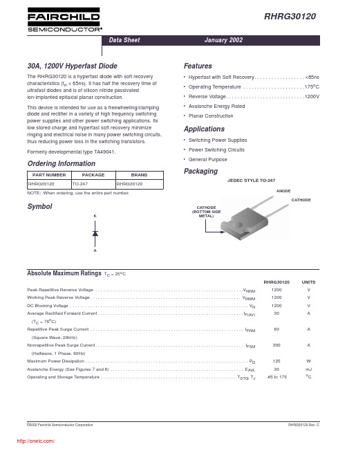
RHRG3012030A,1200V Hyperfast DiodeThe RHRG30120is a hyperfast diode with soft recovery characteristics (t rr <65ns).It has half the recovery time of ultrafast diodes and is of silicon nitride passivated ion-implanted epitaxial planar construction.This device is intended for use as a freewheeling/clamping diode and rectifier in a variety of high frequency switching power supplies and other power switching applications.Its low stored charge and hyperfast soft recovery minimizeringing and electrical noise in many power switching circuits,thus reducing power loss in the switching transistors.Formerly developmental type TA49041.SymbolFeatures•Hyperfast with Soft Recovery..................<65ns •Operating Temperature ......................175o C •Reverse Voltage............................1200V •Avalanche Energy Rated •Planar ConstructionApplications•Switching Power Supplies •Power Switching Circuits •General PurposePackagingJEDEC STYLE TO-247Ordering InformationNOTE:When ordering,use the entire partnumber.KACATHODE CATHODEANODEMETAL)(BOTTOM SIDEAbsolute Maximum Ratings T C =25o CRHRG30120UNITS Peak Repetitive Reverse Voltage ...........................................................V RRM 1200V Working Peak Reverse Voltage............................................................V RWM 1200V DC Blocking Voltage .......................................................................V R 1200V Average Rectified Forward Current..........................................................I F(AV)30A (T C =78o C)Repetitive Peak Surge Current .............................................................I FRM 60A (Square Wave,20kHz)Nonrepetitive Peak Surge Current...........................................................I FSM 300A(Halfwave,1Phase,60Hz)Maximum Power Dissipation .................................................................P D 125W Avalanche Energy (See Figures 7and 8).....................................................E AVL 30mJOperating and Storage Temperature ......................................................T STG ,T J-65to 175o CData SheetJanuary 2002Electrical SpecificationsT C =25o C,Unless Otherwise SpecifiedDEFINITIONSV F =Instantaneous forward voltage (pw =300µs,D =2%).I R =Instantaneous reverse current.t rr =Reverse recovery time (See Figure 6),summation of t a +t b .t a =Time to reach peak reverse current (See Figure 6).t b =Time from peak I RM to projected zero crossing of I RM based on a straight line from peak I RM through 25%of I RM (See Figure 6).R θJC =Thermal resistance junction to case.pw =pulse width.D =duty cycle.Typical Performance CurvesFIGURE 1.FORWARD CURRENT vs FORWARD VOLTAGE FIGURE 2.REVERSE CURRENT vs REVERSE VOLTAGE200100101I F ,F O R W A R D C U R R E N T (A )V F ,FORWARD VOLTAGE (V)0.51.01.52.02.53.03.54.04.5175o C100o C25o C500100101.00.10.010.001020040060080010001200V R ,REVERSE VOLTAGE (V)I R ,R E V E R S E C U R R E N T (µA )175o C100o C 25o CFIGURE 3.t rr ,t a AND t b CURVES vs FORWARD CURRENTFIGURE 4.CURRENT DERATING CURVETypical Performance Curves(Continued)1007550251t ,T I M E (n s )I F ,FORWARD CURRENT (A)1030t rrt at b40302010255075100125150175T C ,CASE TEMPERATURE (o C)I F (A V ),A V E R A G E F O R W A R D C U R R E N T (A )SQ.WAVEDCTest Circuits and WaveformsFIGURE 5.t rr TEST CIRCUITFIGURE 6.t rr WAVEFORMS AND DEFINITIONSFIGURE 7.AVALANCHE ENERGY TEST CIRCUITFIGURE 8.AVALANCHE CURRENT AND VOLTAGEWAVEFORMSV DDV GEV t 1R GDUTCURRENT SENSE+LRV DDR <0.1ΩE AVL =1/2LI 2[V R(AVL)/(V R(AVL)-V DD )]Q 1=IGBT (BV CES >DUT V R(AVL))-V DDQ 1I MAX =1.225A L =40mH I V012分销商库存信息: FAIRCHILD RHRG30120。
FM24V02-GTR;FM24V02-G;中文规格书,Datasheet资料
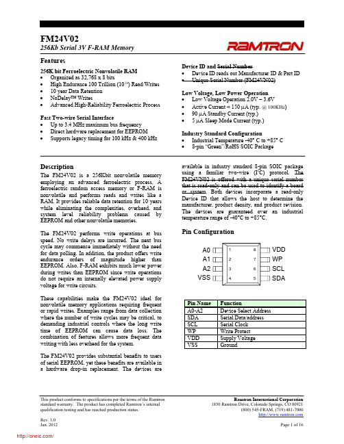
Two-wire Interface
The FM24V02 employs a bi-directional two-wire bus protocol using few pins or board space. Figure 2 illustrates a typical system configuration using the FM24V02 in a microcontroller-based system. The industry standard two-wire bus is familiar to many users but is described in this section. By convention, any device that is sending data onto the bus is the transmitter while the target device for this data is the receiver. The device that is controlling the bus is the master. The master is responsible for generating the clock signal for all operations. Any device on the bus that is being controlled is a slave. The FM24V02 always is a slave device. The bus protocol is controlled by transition states in the SDA and SCL signals. There are four conditions including start, stop, data bit, or acknowledge. Figure 3 illustrates the signal conditions that specify the four states. Detailed timing diagrams are shown in the electrical specifications section.
TLP222G(TP1,F),TLP222G(TP1,F),TLP222G(TP1,F), 规格书,Datasheet 资料
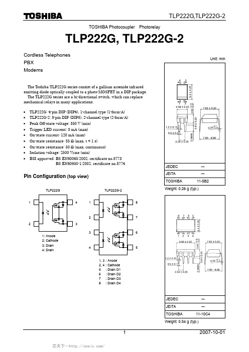
TOSHIBA Photocoupler Photorelay
TLP222G, TLP222G-2
Cordless Telephones PBX Modems
Unit: mm
The Toshiba TLP222G series consist of a gallium arsenide infrared emitting diode optically coupled to a photo-MOSFET in a DIP package.
Allowable On-sate current ION (mA)
TLP222G,TLP222G-2
ION – Ta
240
200
160
120
80
40
0
−20
0
20
40
60
80 100 120
Ambient temperature Ta (°C)
Forward current IF (mA)
100 Ta = 25°C
0
20
40
60
80
100
Ambient temperature Ta (°C)
4
芯天下--/
2007-10-01
On-state resistance RON (Ω)
Switching time tON, tOFF (μs)
50
Isolation Characteristics (Ta = 25°C)
Characteristics Capacitance input to output Isolation resistance
Isolation voltage
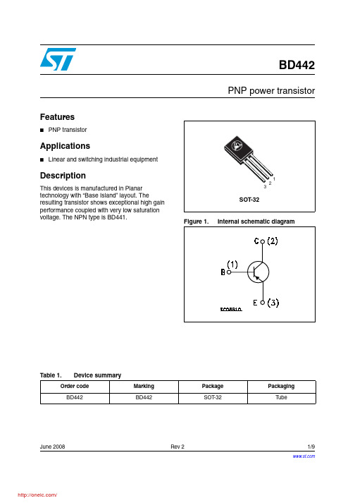
PBRP123ET,215;中文规格书,Datasheet资料
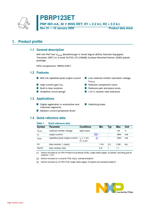
1.Product profile1.1General description800mA PNP low V CEsat Breakthrough In Small Signal (BISS) Resistor-EquippedTransistor (RET) in a small SOT23(TO-236AB) Surface-Mounted Device (SMD) plastic package.NPN complement: PBRN123ET.1.2Features1.3Applications1.4Quick reference data[1]Device mounted on an FR4Printed-Circuit Board (PCB), single-sided copper, tin-plated, mounting pad for collector 1cm 2.[2]Device mounted on a ceramic PCB, Al 2O 3, standard footprint.[3]Device mounted on an FR4PCB, single-sided copper, tin-plated and standard footprint.PBRP123ETPNP 800 mA, 40 V BISS RET; R1 = 2.2 k Ω, R2 = 2.2 k ΩRev. 01 — 16 January 2008Product data sheetI 800mA repetitive peak output current I Low collector-emitter saturation voltage V CEsatI High current gain h FE I Reduces component count I Built-in bias resistors I Reduces pick and place costs I Simplifies circuit designI ±10% resistor ratio toleranceI Digital application in automotive and industrial segmentsI Switching loadsI Medium current peripheral driverTable 1.Quick reference data Symbol ParameterConditions Min Typ Max Unit V CEO collector-emitter voltage open base--−40V I O output current[1][2]--−600mA I ORM repetitive peak output current t p ≤1ms;δ≤0.33[3]--−800mA R1bias resistor 1 (input) 1.54 2.2 2.86k ΩR2/R1bias resistor ratio0.911.12.Pinning information3.Ordering information4.Marking[1]* = -: made in Hong Kong * = p: made in Hong Kong * = t: made in Malaysia * = W: made in China5.Limiting valuesTable 2.PinningPin Description Simplified outline Symbol1input (base)2GND (emitter)3output (collector)123sym003321R1R2Table 3.Ordering informationType numberPackage NameDescriptionVersion PBRP123ET-plastic surface-mounted package; 3leadsSOT23Table 4.Marking codesType number Marking code [1]PBRP123ET*7HTable 5.Limiting valuesIn accordance with the Absolute Maximum Rating System (IEC 60134).Symbol ParameterConditions Min Max Unit V CBO collector-base voltage open emitter -−40V V CEO collector-emitter voltage open base -−40V V EBO emitter-base voltage open collector-−10V V Iinput voltage positive -+10V negative-−22V I O output current[1][2]-−600mA I ORMrepetitive peak output currentt p ≤1ms;δ≤0.33[3]-−800mA[1]Device mounted on an FR4PCB, single-sided copper, tin-plated, mounting pad for collector 1cm 2.[2]Device mounted on a ceramic PCB, Al 2O 3, standard footprint.[3]Device mounted on an FR4PCB, single-sided copper, tin-plated and standard footprint.P tottotal power dissipationT amb ≤25°C[3]-250mW [1]-370mW [2]-570mW T j junction temperature -150°C T amb ambient temperature −55+150°C T stgstorage temperature−65+150°C(1) Ceramic PCB, Al 2O 3 standard footprint (2) FR4PCB, mounting pad for collector 1cm 2(3) FR4PCB, standard footprintFig 1.Power derating curves for SOT23(TO-236AB)Table 5.Limiting values …continuedIn accordance with the Absolute Maximum Rating System (IEC 60134).Symbol ParameterConditions Min Max Unit T amb (°C)−751751252575−25006aaa998200400600P tot (mW)0(1)(2)(3)6.Thermal characteristics[1]Device mounted on an FR4PCB, single-sided copper, tin-plated and standard footprint.[2]Device mounted on an FR4PCB, single-sided copper, tin-plated, mounting pad for collector 1cm 2.[3]Device mounted on a ceramic PCB, Al 2O 3, standard footprint.Table 6.Thermal characteristics Symbol ParameterConditions Min Typ Max Unit R th(j-a)thermal resistance from junction to ambientin free air[1]--500K/W [2]--338K/W [3]--219K/W R th(j-sp)thermal resistance from junction to solder point--105K/WFR4 PCB, standard footprintFig 2.Transient thermal impedance from junction to ambient as a function of pulse duration forSOT23(TO-236AB); typical values006aab000101102103Z th(j-a)(K/W)10−110−51010−210−410210−1t p (s)10−310310.750.500.330.200.010.100.050.020δ = 1FR4 PCB, mounting pad for collector 1cm 2Fig 3.Transient thermal impedance from junction to ambient as a function of pulse duration forSOT23(TO-236AB); typical valuesCeramic PCB, Al 2O 3 standard footprintFig 4.Transient thermal impedance from junction to ambient as a function of pulse duration forSOT23(TO-236AB); typical values006aab001101102103Z th(j-a)(K/W)10−110−51010−210−410210−1t p (s)10−310310.750.500.330.200.010.100.050.020δ = 1006aab002101102103Z th(j-a)(K/W)10−110−51010−210−410210−1t p (s)10−310310.750.500.330.200.010.100.050.020δ = 17.Characteristics[1]Pulse test: t p ≤300µs;δ≤0.02.Table 7.CharacteristicsT amb =25°C unless otherwise specified.Symbol ParameterConditions Min Typ Max Unit I CBO collector-base cut-off currentV CB =−30V;I E =0A--−100nA I CEO collector-emitter cut-off current V CE =−30V;I B =0A --−0.5µA I EBO emitter-base cut-off current V EB =−5V;I C =0A --−2mAh FEDC current gainV CE =−5V;I C =−50mA 70120-V CE =−5V;I C =−300mA [1]180250-V CE =−5V;I C =−600mA[1]170240-V CEsatcollector-emitter saturation voltageI C =−50mA;I B =−2.5mA -−35−45mV I C =−200mA;I B =−10mA -−70−100mV I C =−500mA;I B =−10mA [1]-−200−300mV I C =−600mA;I B =−6mA[1]-−450−750mV V I(off)off-state input voltage V CE =−5V;I C =−100µA −0.6−1−1.8V V I(on)on-state input voltage V CE =−0.3V;I C =−20mA−1−1.3−2V R1bias resistor 1 (input) 1.54 2.2 2.86k ΩR2/R1bias resistor ratio 0.91 1.1C ccollector capacitanceV CB =−10V;I E =i e =0A;f =1MHz-11-pFV CE =−5V (1)T amb =100°C (2)T amb =25°C (3)T amb =−40°CI C /I B =20(1)T amb =100°C (2)T amb =25°C (3)T amb =−40°CFig 5.DC current gain as a function of collectorcurrent; typical valuesFig 6.Collector-emitter saturation voltage as afunction of collector current; typical valuesI C /I B =50(1)T amb =100°C (2)T amb =25°C (3)T amb =−40°CI C /I B =100(1)T amb =100°C (2)T amb =25°C (3)T amb =−40°CFig 7.Collector-emitter saturation voltage as afunction of collector current; typical values Fig 8.Collector-emitter saturation voltage as afunction of collector current; typical values006aab085I C (mA)−10−1−103−102−1−10110102103h FE 10−1(1)(2)(3)006aab086I C (mA)−1−103−102−10−10−1V CEsat (V)−10−2(1)(2)(3)I C (mA)−10−103−102006aab087−10−1−1V CEsat (V)−10−2(1)(2)(3)I C (mA)−10−103−102006aab088−10−1−1V CEsat (V)−10−2(1)(2)(3)8.Package outlineV CE =−0.3V (1)T amb =−40°C (2)T amb =25°C (3)T amb =100°CV CE =−5V (1)T amb =−40°C (2)T amb =25°C (3)T amb =100°CFig 9.On-state input voltage as a function of collectorcurrent; typical values Fig 10.Off-state input voltage as a function of collectorcurrent; typical values006aab089I C (mA)−10−1−103−102−1−10−1−10V I(on)(V)−10−1(1)(2)(3)006aab090I C (mA)−10−1−102−10−1−1−10V I(off)(V)−10−1(1)(2)(3)Fig 11.Package outline SOT23(TO-236AB)04-11-04Dimensions in mm0.450.151.91.10.93.02.82.52.1 1.41.20.480.380.150.091239.Packing information[1]For further information and the availability of packing methods, see Section 13.10.SolderingTable 8.Packing methodsThe indicated -xxx are the last three digits of the 12NC ordering code.[1]Type number Package DescriptionPacking quantity 300010000PBRP123ETSOT234mm pitch, 8mm tape and reel-215-235Fig 12.Reflow soldering footprint SOT23(TO-236AB)Fig 13.Wave soldering footprint SOT23(TO-236AB)solder resistoccupied areasolder landssolder paste Dimensions in mmsot0231.000.60(3x)1.301232.503.000.85 2.702.900.50 (3x)0.60 (3x)3.300.85sot0234.004.60 2.804.501.203.403211.20 (2x)preferred transport direction during solderingDimensions in mmsolder resist occupied areasolder lands11.Revision historyTable 9.Revision historyDocument ID Release date Data sheet status Change notice Supersedes PBRP123ET_120080116Product data sheet--分销商库存信息: NXPPBRP123ET,215。
28202;中文规格书,Datasheet资料

599 Menlo Drive, Suite 100Rocklin, California 95765, USAOffice: (916) 624-8333Fax: (916) 624-8003General: info@Technical: support@Web Site: Educational: Gripper Kit for the Boe-Bot® Robot (#28202)The Gripper KitThis kit allows your Parallax Boe-Bot® Robot to pick up objects. TheBoe-Bot robot (#28132 serial or #28832 USB) is sold separately.Before getting started, take an inventory of the parts in your kit. UseFig #1 to identify each part to the parts list. Once you haveinventoried your kit, proceed to Step #1.11423456791011121315161783Recommended Tools•Small needle nosed pliers•Phillips #2 point screwdriver•Small flat-blade screwdriver• A sharp-tipped hobby knife,such as an X-Acto® knife-OR-A hand drill with 5/64″ bitWARNING!DO NOT use electricscrewdrivers with this kit. Pleaseassemble using hand tools onlyto avoid damaging your Gripper.Step #1: SpacersItem Qty Description 4 (2) Gripper link 5 (2) #4 x 1" spacer• Insert spacers into plastic Gripper links. • Use Fig #2 as a guide to install the spacers. Whendone, the pieces will appear as shown in Fig #3.Fig #2Fig #3Step #2: Gripper LinksItem Qty Description6 (1) Gripper plate7 (2) 4-40 x 1.25" pan head screw8 (2) 4-40 Hex Nut•Be sure the angled portions on top of the plastic links match the angles on top of the Gripper as shown in Fig #5.• Move links and spacers into the Gripper plate, thensecure with 4-40 screws and nuts as shown in Fig #4. • Tighten securely.• Before continuing, double check your work to ensurethat the pieces are angled as in Fig #5.Fig #4 Fig #5Step #3: Foam TapeItem Qty Description14 (4) foam tape• Cut four pieces of foam tape, each 2 inches long. •Apply foam tape to the Gripper plate as shown in Fig #7.This completes the left-side Gripper sub-assembly.Fig #6Fig #7Step #4: Second Gripper Sub-assemblyItem Qty Description4 (2) Gripper link5 (2) #4 x 1" spacer6 (1) Gripper plate7 (2) 4-40 x 1.25" pan head screw8 (2) 4-40 hex nut 14 (4) foam tape• Repeat Steps #1 through #3 to build the right-sideGripper sub-assembly in a similar fashion.• Be sure the angled portions of the links match with theGrippers face to face. Position the pieces exactly as they appear in Fig #8.• Double check your work, then proceed to Step #5.Fig #8•Assemble the Gripper sub-assemblies to the upperand lower linkage plates as shown in Fig #9. In turn, insert each plastic link, a spacer, and secure with 4-40 screws and nuts.• When all four plastic links are installed, tighten securely.•Double check your work against Fig #10. Note that the hinge tabs on the bottom plate face up, while hinge tabs on top plate face down.Step #5: Linkage PlatesItem Qty Description3 (2) linkage plate 5 (4)#4 x 1" spacer 7(4) 4-40 x 1.25" pan head screw 8 (4) 4-40 hex nutStep #6: Control ArmsItem Qty Description 10 (2) control arm 15 (4) 4-40 x ¼" pan head screw• Attach control arms with 4-40 x ¼" screws as shown in Fig #11.•Final assembly must match Fig #12. Double check your work, then proceed to Step #7.Fig #11Fig #12Step #7: E-Z ConnectorsItem Qty Description 13 (2) Brass 0.072 E-Z Connector• Follow the directions on the package to install the E/Z Connector into the control arms. Use the nylon washers, but set the screws aside for now.• Check your work; your final assembly should match Fig #13.Fig #13Step #8: Install Gripper Hinge PlateItem Qty Description1 (1) hinge mount 15 (3) 4-40 x ¼" pan head screw 8 (3) 4-40 hex nutNote: It is recommended that the servos and tires on the Boe-Bot be installed with the wheels biased toward the front of the unit as shown below. This will prevent the Boe-Bot from tipping when it picks up objects.• Attach hinge mount to the Boe-Bot with the 4-40 x ¼" screws and nuts as shown in Fig #14 and Fig #15. • Double check your work against Fig #16.Fig #14 Top ViewFig #15 Bottom ViewFig #16Assembled ViewStep #9: Position Gripper on Boe-BotItem Qty Description(1) Gripper assembly (1) Boe-Bot robot• Remove one wheel to allow for dowel pin installation in the next step, Step #10.• Position the Gripper assembly onto the hinge mount as shown in Fig #17 below.•Place the top hinge tabs over the tabs on the hinge mount so the top of the Gripper stays on the hinge mount.Fig #17Step #10: Insert Dowel Pin Item Qty Description2 (1) dowelpin• Insert dowel pin.•If dowel pin slips in very easily, use needle nose pliers to slightly crimp the center of the hinge plate.• Replace wheel.Fig #18Fig #19Fig #21Step #12: Servo BracketsItem Qty Description16 (2) servo brackets 17 (4) 4-40 x 3/8" pan head screw 8 (4) 4-40 hex nut 11 (1) Parallax Standard Serv o• Attach servo brackets to servo with 4-40 screws and nuts. Make sure the metal brackets are placed below the plastic servo tabs as shown in Fig #22.•The final assembly should match Fig #23. Double check your work, then proceed to Step #13.Note: Only one arm of the servo horn is shown for clarity.Fig #22Fig #23Step #13: Bend Actuator RodItem Qty Description 12 (1) actuator rod•Using the needle nose pliers, bend actuator rod at mid-point. Then bend as shown in Fig #24.Fig #24Step #14: Install Actuator Rod Item Qty Description12 (1) actuatorrod11 (1) Parallax Standard Servo•Thread bent rod through servo horn as shown in Fig #25.Fig #25分销商库存信息: PARALLAX 28202。
LG IPS LED监视器IPS224V IPS234V使用手册说明书

OWNER’S MANUALIPS LED MONITORIPS224V IPS234VPlease read this manual carefully before operating your set and retain it for future reference.IPS LED MONITOR MODEL ENGLISH2TABLE OF CONTENTS Contents3AsseMBLInG AnD PRePAR-InG3 Unpacking4 Parts and buttons5 Setting up the Monitor set5 - Attaching the Stand Base5 - Detaching the Stand Base6 - Mounting on a table6 - Using the cable holder8 - Mounting on a wall9UsInG tHe MonItoR set 9 Connecting to a PC9 - D-SUB connection9 - DVI-D connection9 - HDMI connection11CUstoMIZInG settInGs 12 Customizing Settings12 - Menu Settings13 - P ICTURE14 - C OLOR15 - D ISPLAY15 - V OLUME16 - O THERS17 MY KEY Setting18 FUNC. Setting18 - P ICTURE MODE19 - S UPER ENERGY SAVING20 - D UAL DISPLAY20 - D UAL WEB21 - M Y KEY SETTING 22tRoUBLesHootInG24sPeCIFICAtIons24 IPS224V25 IPS234V26 Preset Modes (Resolution)26 Indicator27PRoPeR PostURe27 Proper posture for using the Monitor set.3ASSEMBLING AND PREPARING AsseMBLInG AnD PRePARInGUnpackingCheck your product box for the following items. If there are any missing accessories, contact the local dealer where you purchased your product. The illustrations in this manual may differ from the actual product4ASSEMBLING AND PREPARING(Power Button)5ASSEMBLING AND PREPARINGAttach the stand Body to the monitor set.Attach the stand Base .Tighten the screw to the right with a coin.setting up the Monitor setAttaching the stand Base1 Place the Monitor set with the screen sidedown on a flat and cushioned surface.2123Detaching the stand Base1 Place the Monitor set with the screen sidedown on a flat and cushioned surface.stand BasePull out the stand Body and stand Basefrom the monitor set.Turn the screw to the left with a coin.Pull out the stand Base .12326ASSEMBLING AND PREPARING7ENG ENGLISHASSEMBLING AND PREPARINGDo not hold this set like below picture.Monitor screen can detach from stand base and injure8ASSEMBLING AND PREPARINGMounting on a wallFor proper ventilation, allow a clearance of 10 cmon each side and from the wall. Detailedinstructions are available from your dealer, see the optional Tilt Wall Mounting Bracket Installation and Setup Guide.If you intend to mount the Monitor set to a wall, attach Wall mounting interface (optional parts) to the back of the set.When you install the Monitor set using a wall mounting interface (optional parts), attach it carefully so it will not drop.1 Please, Use the screw and wall mount interfacein accordance with VESA Standards.2 If you use screw longer than standard, themonitor might be damaged internally.3 If you use improper screw, the product might bedamaged and drop from mounted position. In this case, LG Electronics is not responsible for it.4 VESA compatible.5 Please use VESA standard as below.y 784.8 mm (30.9 inch) and under * Wall Mount Pad Thickness : 2.6 mm * Screw : Φ 4.0 mm x Pitch 0.7 mm x Length 10 mmy 787.4 mm (31.0 inch) and above * Please use VESA standard wall mount pad and screws.10 cmModelVesA (A x B)75 x 75standard screw M4number of screws4IPS224V IPS234V9USING THE MONITOR SETUsInG tHe MonItoR setConnecting to a PCy Your Monitor set supports Plug & Play*. *Plug & Play: A PC recognizes a connected device that users connect to a PC and turn on, without device configuration or user intervention.D-sUB connectionTransmits analog video from your PC to theMonitor set. Connect the PC and the Monitor set with the supplied D-sub 15 pin signal cable as shown in the following illustrations.DVI-D connectionTransmits a digital video signal from your PC to the Monitor set. Connect the PC and the Monitor set with a DVI cable as shown in the following illustrations.HDMI connectionTransmits the digital video and audio signals from your PC or A/V to the Monitor set. Connect the PC or A/V and the Monitor set with the HDMI cable as shown in the following illustrations.10USING THE MONITOR SETCUstoMIZInG settInGs1Press the desired button on the bottom of the Monitor set.2Change the value of the menu item by pressing the buttons on the bottom of the Monitor set.To return to the upper menu or set other menu items, use the up arrow () button.3Select eXIt to leave the OSD menu.y Analog: D-SUB(Analog signal) input. y Digital: DVI-D(Digital signal) input. y HDMI: HDMI(Digital signal) input.PICtURe1Press MenU button on the bottom of the Monitor set to display the MenU OSD.2Select the "neXt MenU" button to enter the more option settings.3Enter to PICtURe by pressing the ▼ button.4Set the options by pressing the ◄ or ► or ▼ buttons.5Select eXIt to leave the OSD menu.To return to the upper menu or set other menu items, use the up arrow () button.DIsPLAY1Press MenUbutton on the bottom of the Monitor setto display the MenU OSD.2Select the "neXt MenU" button to enter the more option settings.3Select DIsPLAY by pressing the ► button.4Enter to DIsPLAY by pressing the ▼ button.5Set the options by pressing the ◄ or ► or ▼ buttons.6Select eXIt to leave the OSD menu.VoLUMe1Press MenU button on the bottom of the Monitor set to display the MenU OSD.2Select the "neXt MenU" button to enter the moreoption settings.3Select VoLUMe by pressing the ► button.4Enter to VoLUMe by pressing the ▼ button.5Set the options by pressing the ◄ or ► buttons.6Select eXIt to leave the OSD menu.To return to the upper menu or set other menu items, use the up arrow () button.otHeRs1Press MenU button on the bottom of the Monitor set to display the MenU OSD.2Select the "neXt MenU" button to enter the more option settings.3Select otHeRs by pressing the ► button.4Enter to otHeRs by pressing the ▼ button.5Set the options by pressing the ◄ or ► or ▼ buttons.6Select eXIt to leave the OSD menu.To return to the upper menu or set other menu items, use the up arrow () button.ENG ENGLISH Each option is explained below.FUnC. settingPICtURe MoDe1Press FUnC. button on the bottom of the Monitor set to display the FUnC. OSD.2Enter to PICtURe MoDe by pressing the ▼ button. 3Set the options by pressing the ◄ or ► buttons.4 Select eXIt to leave the OSD menu.To return to theupper menu or set other menu items, use the uparrow()button.Each option is explained below.ENG ENGLISHsUPeR eneRGY sAVInG1 Press FUnC. button on the bottom of the Monitor set todisplay the FUnC. OSD. 2 Select sUPeR eneRGY sAVInG by pressing the ► button. 3 Enter to sUPeR eneRGY sAVInG by pressing the ▼ button.4 Set the options by pressing the ◄ or ► or ▼buttons.5 Select eXIt toleave the OSD menu.To return to the upper menu or set other menu items, use the up arrow() button.* Before using below functions, please install DUAL PACKAGE programme. Each option is explained below.ENG ENGLISHEach option is explained below.MY KeY settInG1 Press FUnC. button on the bottom of the Monitorset to display the FUnC. OSD.2 Select MY KeY settInG by pressing the ► button.3 Enter to MY KeY settInG by pressing the ▼button.4 Set the options by pressing the ◄ or ► buttons.5 Select eXIt toleave the OSD menu.To return to the upper menu or set other menu items, use the up arrow () button.22SPECIFICATIONS tRoUBLesHootInG23 SPECIFICATIONSENG ENGLISH24SPECIFICATIONSsPeCIFICAtIonsDisplay screen type54.6 cm (21.5 inch) Flat Panel Active matrix-TFT LCDAnti-Glare coatingVisible diagonal size: 54.6 cmPixel Pitch0.247 mm x 0.247 mm (Pixel Pitch)sync Input Horizontal Frequency30 kHz to 83 kHz (Automatic)Vertical Frequency56Hz to 75Hz (D-SUB, DVI-D)56Hz to 61Hz (HDMI)Input Form Separate Sync. DigitalVideo Input signal Input15 pin D-SUB Connector /DVI-D Connector (Digital)HDMI ConnectorInput Form RGB Analog (0.7 Vp-p/ 75 ohm), DigitalResolution Max D-SUB(Analog) : 1920 x 1080 @ 60 HzDVI / HDMI (Digital) : 1920 x 1080 @ 60 HzRecommend VESA 1920 x 1080 @ 60 HzPlug & Play DDC 2B(Analog,Digital,HDMI)Power Consumption On Mode : 25 W(Typ.) Sleep Mode ≤ 0.3 W Off Mode ≤ 0.3 WPower Input19 V 1.2 AAC-DC Adapter Type ADS-40SG-19-3 19025G, manufactured by SHENZHEN HONOR ELECTRONICor Type ADS-40FSG-19 19025GPG-1, manufactured by SHENZHEN HONOR ELECTRONICor Type ADS-40FSG-19 19025GPBR-1, manufactured by SHENZHEN HONOR ELECTRONICor Type ADS-40FSG-19 19025GPI-1, manufactured by SHENZHEN HONOR ELECTRONICor Type ADS-40FSG-19 19025GPCU-1, manufactured by SHENZHEN HONOR ELECTRONICor Type LCAP21, manufactured by LIEN CHANG ELECTRONIC ENTERPRISEor Type LCAP26-A, manufactured by LIEN CHANG ELECTRONIC ENTERPRISEor Type LCAP26-E, manufactured by LIEN CHANG ELECTRONIC ENTERPRISEor Type LCAP26-I, manufactured by LIEN CHANG ELECTRONIC ENTERPRISEor Type LCAP26-B, manufactured by LIEN CHANG ELECTRONIC ENTERPRISEoUtPUt: 19 V 1.3 ADimensions (width x Height x Depth)with stand50.9 cm x 38.7 cm x 18.1 cm without stand50.9 cm x 31.3 cm x 5.5 cmweight 2.6 kg tilt Range-5° to 20°environmental conditions operating temperatureoperating Humidity10°C to 35 °C10 % to 80 %storage temperaturestorage Humidity-20°C to 60 °C5 % to 90 % non-Condensingstand Base Attached ( ), Detached (O)Power cord Wall-outlet typeProduct specifications shown above may be changed without prior notice due to upgrade of product functions.IPs224V25SPECIFICATIONS sPeCIFICAtIonsDisplay screen type58.4 cm (23 inch) Flat Panel Active matrix-TFT LCDAnti-Glare coatingVisible diagonal size: 58.4 cmPixel Pitch0.265 mm x 0.265 mm (Pixel Pitch)sync Input Horizontal Frequency30 kHz to 83 kHz (Automatic)Vertical Frequency56Hz to 75Hz (D-SUB, DVI-D)56Hz to 61Hz (HDMI)Input Form Separate Sync. DigitalVideo Input signal Input15 pin D-SUB Connector /DVI-D Connector (Digital)HDMI ConnectorInput Form RGB Analog (0.7 Vp-p/ 75 ohm), DigitalResolution Max D-SUB(Analog) : 1920 x 1080 @ 60 HzDVI / HDMI (Digital) : 1920 x 1080 @ 60 HzRecommend VESA 1920 x 1080 @ 60 HzPlug & Play DDC 2B(Analog,Digital,HDMI)Power Consumption On Mode : 27 W(Typ.) Sleep Mode ≤ 0.3 W Off Mode ≤ 0.3 WPower Input19 V 1.6 AAC-DC Adapter Type ADS-40SG-19-3 19032G, manufactured by SHENZHEN HONOR ELECTRONIC or Type ADS-40FSG-19 19032GPG-1, manufactured by SHENZHEN HONOR ELECTRONICor Type ADS-40FSG-19 19032GPBR-1, manufactured by SHENZHEN HONOR ELECTRONICor Type ADS-40FSG-19 19032GPI-1, manufactured by SHENZHEN HONOR ELECTRONICor Type ADS-40FSG-19 19032GPCU-1, manufactured by SHENZHEN HONOR ELECTRONICor Type LCAP21A, manufactured by LIEN CHANG ELECTRONIC ENTERPRISEor Type LCAP26A-A, manufactured by LIEN CHANG ELECTRONIC ENTERPRISEor Type LCAP26A-E, manufactured by LIEN CHANG ELECTRONIC ENTERPRISEor Type LCAP26A-I, manufactured by LIEN CHANG ELECTRONIC ENTERPRISEor Type LCAP26A-B, manufactured by LIEN CHANG ELECTRONIC ENTERPRISEoUtPUt: 19 V 1.7 ADimensions (width x Height x Depth)with stand54.4 cm x 40.6 cm x 18.1 cm without stand54.4 cm x 33.2 cm x 5.5 cmweight 2.9 kg tilt Range-5° to 20°environmental conditions operating temperatureoperating Humidity10°C to 35 °C10 % to 80 %storage temperaturestorage Humidity-20°C to 60 °C5 % to 90 % non-Condensingstand Base Attached ( ), Detached (O)Power cord Wall-outlet typeProduct specifications shown above may be changed without prior notice due to upgrade of product functions.IPs234V26SPECIFICATIONSPreset Modes (Resolution) IPs224V/IPs234VHDMI tIMInGIndicator27PROPER POSTUREProper posture for using the Monitor set.PRoPeR PostUReangle.Make sure to read the Safety Precautions before using the product.Keep the Owner’s Manual (CD) in an accessible place for future reference.The model and serial number of the SET is located on the back and one side of the SET . Record it below should you ever need service.As an ENERGY STAR Partner LGE U. S. A.,Inc. has determined that this product meets the ENERGY STAR guidelines for energy efficiency.ENERGY STAR is a set of power-saving guidelines issued by the U.S.Environmental Protection Agency(EPA).MODELSERIAL。
INFINITER LR-22GR 中文說明書
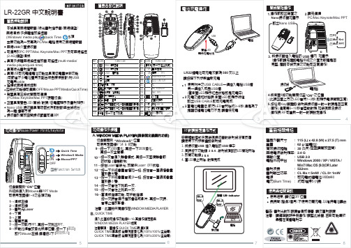
接收機
電腦
4.將側面4段功能開關切至“ON”之位置 (此時正面上方之LED會閃1~2秒,即顯示電源開關正常)
5.按任何Key鍵確認(發射與接收器一對一對碼是否正常 運作),通常等5~10秒會自動對頻,如發現無法接收 運作時,RF可重新一對一對碼設定操作.
4
RF對碼設定操作方式
安裝驅動程式後若發現接收器對發射機沒有反應 請使用下列步驟重設發射機 1.將接收器USB 插入電腦的 USB 埠中 2.同時按下功能鍵 2 & 6 ,發射機頂部的LED開始閃爍 3.放開功能鍵 2 & 6 4.當LED停止閃爍,對頻完成
Win7/ Mac OS (9.0)OR Later
雷射波長 : 532nm
雷射輸出功率 : CL IIIa < 5mW / CL II< 1mW
電源
: 可充電式鋰電池(400mAH)
電力(Burn Time) : 約可維持5小時
使用與相關資訊
使用結束,請切至OFF位置 長時間(超過3個月)不使用仍需充電,以維持電池壽命
㕾㕿㕞㕦 㖛㖕㖩
࿁ᇁ㕐㕼㕵㕴㕐㖙㖞㖔㖙㖓㖑㖤㖟㖢
㕾㕿㕞㕢 㖛㖕㖩
30CM 接收器
電腦
產品相關規格
產品外觀尺寸 : 115 (L) x 42.8 (W) x 27.5 (T) mm 重量 : 62 g(含電池) 有效接收距離 : 30 公尺(在空曠開放空間) 無線電波發射頻率: 2.4 G 傳輸介面 : USB 2.0 電腦系統平台 : Windows 2000 / XP / VISTA /
2 充電之飽和狀態時,側面LED即顯示綠燈 取出USB CABLE即可充電完成.
3 當電池電量低,前方LED會閃爍約3~6秒,這是為了 提醒您鋰電池電力不足,請儘快充電.
GP2S22中文资料
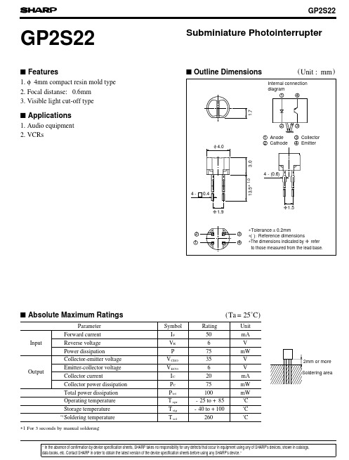
3
s Precautions for Use
( 1 ) Perform soldering manually ( 2 ) Please refrain from soldering under preheating and refrain from soldering by reflow. ( 3 ) As for other general cautions, refer to the chapter “ Precautions for Use”.
Input Output Output td tr ts
Relative collector current ( % )
80
60
Input
10% 90% tf
40
20
0 0
1
2
3
4
5
Distance between GP2S22 and test card d ( mm )
Fig.10 Relative Collector Current vs. Card Moving Distance
V CE= 20V
Collector dark current I CEO ( A)
2
10 - 7
5 2
10 - 8
5 2
10
-9
1
ts
5 2
-10
10
0.1 25 50 75 Ambient temperature T a ( ˚C) 100 0.1 1 10 100 Load resistance R L ( kΩ ) 1000
100 d= 1mm I F = 4mA V CE = 2V T a = 25˚C
Distance Characteristics Test Condition
IPS-MOSFET 功率场效应管系列产品目录
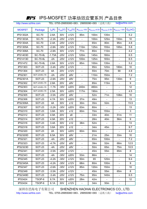
IPS-MOSFET 功率场效应管系列 产品目录
TEL: 0755-29955080~083、29955090~093 (总机八线) tw@
MOSFET
Package
ID(A) VDS(V) VGS(V) RDS(ON)-10V RDS(ON)-4.5V RDS(ON)-2.5V RDS(ON)-1.8V QG(nC)
65 80m 120m 45m 95m 42m 34m
135m 125m 80m 155m 110m 180m 165m 135m 120m 70m 150m 95m 115m
71m 52m 155m 40m 40m 45m 25m 100m 52m 65m 55m 120m 100m 150m 55m 140m 50m
-
6.5
-
12
-
深圳市浩海电子有限公司 SHENZHEN HAOHAI ELECTRONICS CO., LTD.
TEL: 0755-29955080~083、29955090~093 (总机八线) tw@
IPS-MOSFET 功率场效应管系列 产品目录
TEL: 0755-29955080~083、29955090~093 (总机八线) tw@
IPS-MOSFET 功率场效应管系列 产品目录
TEL: 0755-29955080~083、29955090~093 (总机八线) tw@
SOP-8
5.7A 40V ±20V 36m
59m
-
-
9
IPS4942
SOP-8
7A 40V ±20V 23m
33m
-
-
BLF6G22S-45,112;中文规格书,Datasheet资料

(RoHS)
/
NXP Semiconductors
BLF6G22S-45
Power LDMOS transistor
1.3 Applications
I RF power amplifiers for W-CDMA base stations and multicarrier applications in the 2000 MHz to 2200 MHz frequency range
Min 65
1.4 1.65 -
-
Typ -
1.9 2.15 12.5
5 0.2
Max -
2.4 2.65 1.5 -
150 -
Unit V
V V µA A
nA S Ω
7. Application information
Table 7. Application information
Mode of operation: 2-carrier W-CDMA; PAR 7.5 dB at 0.01 % probability on CCDF; 3GPP test
PL-22G说明书(修改版)
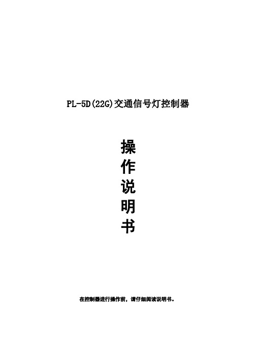
PL-5D(22G)交通信号灯控制器操作说明书在控制器进行操作前,请仔细阅读说明书。
目录1 系统显示状态说明 (2)2 系统运行状态说明 (2)2.1 时间调节 (2)2.2 卫星数目显示(仅GPS型有此功能) (2)2.3 模式切换 (2)2.4 手动控制 (3)2.5 恢复出厂设置 (3)3 系统调试状态说明 (3)3.1 配时调节 (3)3.2 相位过渡参数调节 (4)3.3 相位放行灯组调节 (5)3.4 模式自定义调节 (6)4 附录: (7)4.1 运行模式调整方法范例 (7)4.2 默认模式表 (8)4.3 默认相位表 (10)1系统显示状态说明本系统有2个显示状态:系统运行状态和系统调试状态。
系统运行状态指控制器在正常运行状态下的灯态调度状态;系统调试状态指控制器进入到各参数设置状态下,如配时、相位等状态。
2系统运行状态说明面板数码管与指示灯代码与位置对应图如图所示,控制器在正常运行状态下①②数码管显示的是当前相位绿灯到计时,③④⑤⑥数码管显示的是当前北京时间。
2.1 时间调节按键“时+”、“时-”调节时间小时部分,“分+”、“分-”调节时间分钟部分。
2.2 卫星数目显示(仅GPS型有此功能)按键“A”, ①②瞬间显示当前能使用卫星总数。
2.3 模式切换按键“功能下”切换模一/模二,按键“功能上”切换模式/黄闪。
2.4 手动控制1、按“步进”键,跳过当前相位到下一相位继续运行。
2、按“手动”键,控制器跳出自动运行状态进入到手动控制状态,按“步进”键切换到所要控制的相位(始终保持该相位状态)。
要退出手动控制状态到自动运行状态,再按“手动”键即可。
2.5 恢复出厂设置在控制器关机状态下,按住“手动”键再开启控制机电源,听到一声长“嘀”,系统恢复至出厂设置。
3系统调试状态说明注:在您进行系统调节前,请先确认控制器要分配的时段数,每个时段的相位数,每个相位的放行时间,以及每个相位的过度参数等信息。
TL022CPSR,TL022CPSR,TL022CP,TL022CDR,TL022CDRE4,TL022CDRG4,TL022CPSRE4, 规格书,Datasheet 资料

PACKAGING INFORMATIONOrderable Device Status(1)PackageType PackageDrawingPins PackageQtyEco Plan(2)Lead/Ball Finish MSL Peak Temp(3)TL022CD ACTIVE SOIC D875Green(RoHS&no Sb/Br)CU NIPDAU Level-1-260C-UNLIMTL022CDE4ACTIVE SOIC D875Green(RoHS&no Sb/Br)CU NIPDAU Level-1-260C-UNLIMTL022CDE4ACTIVE SOIC D875Green(RoHS&no Sb/Br)CU NIPDAU Level-1-260C-UNLIMTL022CDE4ACTIVE SOIC D875Green(RoHS&no Sb/Br)CU NIPDAU Level-1-260C-UNLIMTL022CDG4ACTIVE SOIC D875Green(RoHS&no Sb/Br)CU NIPDAU Level-1-260C-UNLIMTL022CDG4ACTIVE SOIC D875Green(RoHS&no Sb/Br)CU NIPDAU Level-1-260C-UNLIMTL022CDG4ACTIVE SOIC D875Green(RoHS&no Sb/Br)CU NIPDAU Level-1-260C-UNLIMTL022CDR ACTIVE SOIC D82500Green(RoHS&no Sb/Br)CU NIPDAU Level-1-260C-UNLIMTL022CDR ACTIVE SOIC D82500Green(RoHS&no Sb/Br)CU NIPDAU Level-1-260C-UNLIMTL022CDR ACTIVE SOIC D82500Green(RoHS&no Sb/Br)CU NIPDAU Level-1-260C-UNLIMTL022CDRE4ACTIVE SOIC D82500Green(RoHS&no Sb/Br)CU NIPDAU Level-1-260C-UNLIMTL022CDRE4ACTIVE SOIC D82500Green(RoHS&no Sb/Br)CU NIPDAU Level-1-260C-UNLIMTL022CDRE4ACTIVE SOIC D82500Green(RoHS&no Sb/Br)CU NIPDAU Level-1-260C-UNLIMTL022CDRG4ACTIVE SOIC D82500Green(RoHS&no Sb/Br)CU NIPDAU Level-1-260C-UNLIMTL022CDRG4ACTIVE SOIC D82500Green(RoHS&no Sb/Br)CU NIPDAU Level-1-260C-UNLIMTL022CDRG4ACTIVE SOIC D82500Green(RoHS&no Sb/Br)CU NIPDAU Level-1-260C-UNLIMTL022CP ACTIVE PDIP P850Pb-Free(RoHS)CU NIPDAU N/A for Pkg TypeTL022CP ACTIVE PDIP P850Pb-Free(RoHS)CU NIPDAU N/A for Pkg TypeTL022CP ACTIVE PDIP P850Pb-Free(RoHS)CU NIPDAU N/A for Pkg TypeTL022CPE4ACTIVE PDIP P850Pb-Free(RoHS)CU NIPDAU N/A for Pkg TypeTL022CPE4ACTIVE PDIP P850Pb-Free(RoHS)CU NIPDAU N/A for Pkg TypeTL022CPE4ACTIVE PDIP P850Pb-Free(RoHS)CU NIPDAU N/A for Pkg TypeTL022CPSR ACTIVE SO PS82000Green(RoHS&no Sb/Br)CU NIPDAU Level-1-260C-UNLIMTL022CPSR ACTIVE SO PS82000Green(RoHS&no Sb/Br)CU NIPDAU Level-1-260C-UNLIMTL022CPSR ACTIVE SO PS82000Green(RoHS&no Sb/Br)CU NIPDAU Level-1-260C-UNLIMOrderable Device Status(1)PackageType PackageDrawingPins PackageQtyEco Plan(2)Lead/Ball Finish MSL Peak Temp(3)TL022CPSRE4ACTIVE SO PS82000Green(RoHS&no Sb/Br)CU NIPDAU Level-1-260C-UNLIMTL022CPSRE4ACTIVE SO PS82000Green(RoHS&no Sb/Br)CU NIPDAU Level-1-260C-UNLIMTL022CPSRE4ACTIVE SO PS82000Green(RoHS&no Sb/Br)CU NIPDAU Level-1-260C-UNLIMTL022CPSRG4ACTIVE SO PS82000Green(RoHS&no Sb/Br)CU NIPDAU Level-1-260C-UNLIMTL022CPSRG4ACTIVE SO PS82000Green(RoHS&no Sb/Br)CU NIPDAU Level-1-260C-UNLIMTL022CPSRG4ACTIVE SO PS82000Green(RoHS&no Sb/Br)CU NIPDAU Level-1-260C-UNLIM(1)The marketing status values are defined as follows:ACTIVE:Product device recommended for new designs.LIFEBUY:TI has announced that the device will be discontinued,and a lifetime-buy period is in effect.NRND:Not recommended for new designs.Device is in production to support existing customers,but TI does not recommend using this part in a new design.PREVIEW:Device has been announced but is not in production.Samples may or may not be available.OBSOLETE:TI has discontinued the production of the device.(2)Eco Plan-The planned eco-friendly classification:Pb-Free(RoHS),Pb-Free(RoHS Exempt),or Green(RoHS&no Sb/Br)-please check /productcontent for the latest availability information and additional product content details.TBD:The Pb-Free/Green conversion plan has not been defined.Pb-Free(RoHS):TI's terms"Lead-Free"or"Pb-Free"mean semiconductor products that are compatible with the current RoHS requirements for all6substances,including the requirement that lead not exceed0.1%by weight in homogeneous materials.Where designed to be soldered at high temperatures,TI Pb-Free products are suitable for use in specified lead-free processes.Pb-Free(RoHS Exempt):This component has a RoHS exemption for either1)lead-based flip-chip solder bumps used between the die and package,or2)lead-based die adhesive used between the die and leadframe.The component is otherwise considered Pb-Free(RoHS compatible)as defined above.Green(RoHS&no Sb/Br):TI defines"Green"to mean Pb-Free(RoHS compatible),and free of Bromine(Br)and Antimony(Sb)based flame retardants(Br or Sb do not exceed0.1%by weight in homogeneous material)(3)MSL,Peak Temp.--The Moisture Sensitivity Level rating according to the JEDEC industry standard classifications,and peak solder temperature.Important Information and Disclaimer:The information provided on this page represents TI's knowledge and belief as of the date that it is provided.TI bases its knowledge and belief on information provided by third parties,and makes no representation or warranty as to the accuracy of such information.Efforts are underway to better integrate information from third parties.TI has taken and continues to take reasonable steps to provide representative and accurate information but may not have conducted destructive testing or chemical analysis on incoming materials and chemicals.TI and TI suppliers consider certain information to be proprietary,and thus CAS numbers and other limited information may not be available for release.In no event shall TI's liability arising out of such information exceed the total purchase price of the TI part(s)at issue in this document sold by TI to Customer on an annual basis.TAPE AND REEL INFORMATION*All dimensions are nominalDevicePackage Type Package Drawing Pins SPQReel Diameter (mm)Reel Width W1(mm)A0(mm)B0(mm)K0(mm)P1(mm)W (mm)Pin1Quadrant TL022CDR SOIC D 82500330.012.4 6.4 5.2 2.18.012.0Q1TL022CPSRSOPS82000330.016.48.26.62.512.016.0Q1*All dimensions are nominalDevice Package Type Package Drawing Pins SPQ Length(mm)Width(mm)Height(mm) TL022CDR SOIC D8*******.5338.120.6TL022CPSR SO PS82000367.0367.038.0芯天下--/IMPORTANT NOTICETexas Instruments Incorporated and its subsidiaries(TI)reserve the right to make corrections,enhancements,improvements and other changes to its semiconductor products and services per JESD46C and to discontinue any product or service per JESD48B.Buyers should obtain the latest relevant information before placing orders and should verify that such information is current and complete.All semiconductor products(also referred to herein as“components”)are sold subject to TI’s terms and conditions of sale supplied at the time of order acknowledgment.TI warrants performance of its components to the specifications applicable at the time of sale,in accordance with the warranty in TI’s terms and conditions of sale of semiconductor products.Testing and other quality control techniques are used to the extent TI deems necessary to support this warranty.Except where mandated by applicable law,testing of all parameters of each component is not necessarily performed.TI assumes no liability for applications assistance or the design of Buyers’products.Buyers are responsible for their products and applications using TI components.To minimize the risks associated with Buyers’products and applications,Buyers should provide adequate design and operating safeguards.TI does not warrant or represent that any license,either express or implied,is granted under any patent right,copyright,mask work right,or other intellectual property right relating to any combination,machine,or process in which TI components or services are rmation published by TI regarding third-party products or services does not constitute a license to use such products or services or a warranty or endorsement e of such information may require a license from a third party under the patents or other intellectual property of the third party,or a license from TI under the patents or other intellectual property of TI.Reproduction of significant portions of TI information in TI data books or data sheets is permissible only if reproduction is without alteration and is accompanied by all associated warranties,conditions,limitations,and notices.TI is not responsible or liable for such altered rmation of third parties may be subject to additional restrictions.Resale of TI components or services with statements different from or beyond the parameters stated by TI for that component or service voids all express and any implied warranties for the associated TI component or service and is an unfair and deceptive business practice. TI is not responsible or liable for any such statements.Buyer acknowledges and agrees that it is solely responsible for compliance with all legal,regulatory and safety-related requirements concerning its products,and any use of TI components in its applications,notwithstanding any applications-related information or support that may be provided by TI.Buyer represents and agrees that it has all the necessary expertise to create and implement safeguards which anticipate dangerous consequences of failures,monitor failures and their consequences,lessen the likelihood of failures that might cause harm and take appropriate remedial actions.Buyer will fully indemnify TI and its representatives against any damages arising out of the use of any TI components in safety-critical applications.In some cases,TI components may be promoted specifically to facilitate safety-related applications.With such components,TI’s goal is to help enable customers to design and create their own end-product solutions that meet applicable functional safety standards and requirements.Nonetheless,such components are subject to these terms.No TI components are authorized for use in FDA Class III(or similar life-critical medical equipment)unless authorized officers of the parties have executed a special agreement specifically governing such use.Only those TI components which TI has specifically designated as military grade or“enhanced plastic”are designed and intended for use in military/aerospace applications or environments.Buyer acknowledges and agrees that any military or aerospace use of TI components which have not been so designated is solely at the Buyer's risk,and that Buyer is solely responsible for compliance with all legal and regulatory requirements in connection with such use.TI has specifically designated certain components which meet ISO/TS16949requirements,mainly for automotive ponents which have not been so designated are neither designed nor intended for automotive use;and TI will not be responsible for any failure of such components to meet such requirements.Products ApplicationsAudio /audio Automotive and Transportation /automotiveAmplifiers Communications and Telecom /communicationsData Converters Computers and Peripherals /computersDLP®Products Consumer Electronics /consumer-appsDSP Energy and Lighting /energyClocks and Timers /clocks Industrial /industrialInterface Medical /medicalLogic Security /securityPower Mgmt Space,Avionics and Defense /space-avionics-defense Microcontrollers Video and Imaging /videoRFID OMAP Mobile Processors /omap TI E2E Community Wireless Connectivity /wirelessconnectivityMailing Address:Texas Instruments,Post Office Box655303,Dallas,Texas75265Copyright©2012,Texas Instruments Incorporated。
高性能开关电源同步整流芯片 LPSR100说明书

概述LPSR100为高性能的开关电源100V 同步整流系列产品,兼容多种开关电源控制系统。
LPSR100支持DCM 和CCM 多种工作模式。
LPSR100采用专利的整流管开通判定技术,可以有效的避免因激磁振荡引起的驱动芯片误开通。
LPSR100具有极快的关断速度,可以大幅度降低在CCM 工作条件下因关断延迟造成的效率损失。
LPSR100集成VCC 供电技术,在不需要辅助绕组供电的情况下,保证芯片VCC 不会欠压。
LPSR100采用TO220-3L/TO252-2L/SOP8L/PDFN5*6封装。
特点⏹开关电源同步整流应用⏹兼容DCM 和CCM 多种工作模式⏹内置100V 耐压功率管⏹专利的整流管开通技术⏹集成VCC 供电⏹芯片供电欠压保护⏹芯片过压钳位⏹外围元器件少应用⏹充电器和适配器的同步整流⏹正激控制器和反激控制器⏹其他开关电源控制系统典型应用图1LPSR100反激典型应用定购信息图2管脚封装图管脚描述A JA注3:人体模型,100pF电容通过1.5KΩ电阻放电。
电气参数(注4,5)(无特别说明情况下,V CC=6V,T A=25℃)电气特性图内部结构框图图3LPSR100内部框图应用信息LPSR100为高性能的开关电源100V 同步整流系列产品,兼容多种开关电源控制系统,支持DCM ,CCM 多种工作模式。
LPSR100采用专利的整流管开关技术,可以有效的避免因激磁振荡引起的驱动芯片误动作。
LPSR100集成VCC 供电技术,在不需要辅助绕组供电的情况下,保证芯片VCC 不会欠压。
启动当系统上电后,通过内置MOS 的体二极管对输出电容充电,输出电压上升。
LPSR100通过D 脚连接输出电压,当输出电压上升时,经过芯片内部供电电路,给VCC 电容充电,当VCC 的电压充到开启阈值电压时,芯片内部控制电路开始工作,MOS 正常的导通和关断。
MOS 正常的导通时,电流不再从体二极管流过,而从MOS 的沟道流过。
BD442;中文规格书,Datasheet资料
-0.1
mA
பைடு நூலகம்
-1
mA
Collector-emitter VCEO(sus)(1) sustaining voltage (IB = 0) VCE(sat)(1) VBE(1) Collector-emitter saturation voltage Base-emitter voltage
IC = -100 mA
0016114E
7/9
/
Revision history
BD442
4
Table 4.
Revision history
Document revision history
Revision 1 2 Initial Release Removed BD440 Changes
Electrical characteristics (curves)
Figure 2. DC current gain Figure 3. DC current gain
Figure 4.
Collector-emitter saturation voltage
Figure 5.
Base-emitter saturation voltage
/
Absolute maximum ratings
BD442
1
Absolute maximum ratings
Table 2.
Symbol VCBO VCES VCEO VEBO IC ICM IB PTOT Tstg TJ
Absolute maximum ratings
Date 08-Feb-2008 09-Jun-2008
8/9
/
BD442
MPTE-22G资料

1N6373 − 1N6381 Series (ICTE−5 − ICTE−36,MPTE−5 − MPTE−45)1500 Watt Peak Power Mosorb t Zener Transient Voltage SuppressorsUnidirectional*Mosorb devices are designed to protect voltage sensitive components from high voltage, high−energy transients. They have excellent clamping capability, high surge capability, low zener impedance and fast response time. These devices are ON Semiconductor’s exclusive, cost-effective, highly reliable Surmetic t axial leaded package and are ideally-suited for use in communication systems, numerical controls, process controls,medical equipment, business machines, power supplies and many other industrial/consumer applications, to protect CMOS, MOS and Bipolar integrated circuits.Specification Features•Working Peak Reverse V oltage Range − 5.0 V to 45 V •Peak Power − 1500 Watts @ 1 ms•ESD Rating of Class 3 (>16 KV) per Human Body Model •Maximum Clamp V oltage @ Peak Pulse Current •Low Leakage < 5 m A Above 10 V •Response Time is Typically < 1 ns •Pb−Free Packages are Available*Mechanical CharacteristicsCASE: V oid-free, transfer-molded, thermosetting plasticFINISH: All external surfaces are corrosion resistant and leads arereadily solderableMAXIMUM LEAD TEMPERATURE FOR SOLDERING PURPOSES:230°C, 1/16″ from the case for 10 secondsPOLARITY: Cathode indicated by polarity band MOUNTING POSITION: Any*For additional information on our Pb−Free strategy and soldering details, please download the ON Semiconductor Soldering and Mounting Techniques Reference Manual, SOLDERRM/D.†For information on tape and reel specifications, including part orientation and tape sizes, please refer to our Tape and Reel PackagingSpecifications Brochure, BRD8011/D.Device Package Shipping †ORDERING INFORMATIONMPTE−xx, G Axial Lead (Pb−Free)500 Units/Box MPTE−xxRL4, G Axial Lead (Pb−Free)1500/T ape & Reel ICTE−xx, G Axial Lead (Pb−Free)500 Units/Box ICTE−xxRL4, G Axial Lead (Pb−Free)1500/T ape & Reel 1N63xx, GAxial Lead (Pb−Free)500 Units/Box 1N63xxRL4, GAxial Lead (Pb−Free)1500/T ape & ReelMAXIMUM RATINGSRating Symbol Value Unit Peak Power Dissipation (Note 1)@ T L≤ 25°CP PK1500WSteady State Power Dissipation @ T L≤ 75°C, Lead Length = 3/8″Derated above T L = 75°C P D 5.020WmW/°CThermal Resistance, Junction−to−Lead R q JL20°C/W Forward Surge Current (Note 2)@ T A = 25°CI FSM200A Operating and Storage Temperature Range T J, T stg−65 to +175°CMaximum ratings are those values beyond which device damage can occur. Maximum ratings applied to the device are individual stress limit values (not normal operating conditions) and are not valid simultaneously. If these limits are exceeded, device functional operation is not implied, damage may occur and reliability may be affected.1.Nonrepetitive current pulse per Figure 5 and derated above T A = 25°C per Figure2.2.1/2 sine wave (or equivalent square wave), PW = 8.3 ms, duty cycle = 4 pulses per minute maximum.*Please see 1N6382 – 1N6389 (ICTE−10C − ICTE−36C, MPTE−8C − MPTE−45C) for Bidirectional Devices.ELECTRICAL CHARACTERISTICS (T A = 25°C unlessotherwise noted, V F = 3.5 V Max. @ I F (Note 3) = 100 A)Symbol ParameterI PP Maximum Reverse Peak Pulse CurrentV C Clamping Voltage @ I PPV RWM Working Peak Reverse VoltageI R Maximum Reverse Leakage Current @ V RWMV BR Breakdown Voltage @ I TI T Test CurrentQ V BR Maximum Temperature Variation of V BRI F Forward CurrentV F Forward Voltage @ I FUni−Directional TVSELECTRICAL CHARACTERISTICS (T A = 25°C unless otherwise noted, V F = 3.5 V Max. @ I F (Note 3)= 100 A) JEDECDevice†(ON Device)DeviceMarkingV RWM(Note 4)I R @V RWMBreakdown Voltage V C @ I PP(Note 6)V C (Volts) (Note 6)Q V BRV BR (Note 5) (Volts)@ I T V C I PP@ I PP =1 A@ I PP =10 A(Volts)(m A)Min Nom Max(mA)(Volts)(A)(mV/°C)1N6373, G (MPTE−5, G)1N6373MPTE−5 5.0300 6.0−− 1.09.41607.17.5 4.01N6374, G (MPTE−8, G)1N6374MPTE−88.0259.4−− 1.01510011.311.58.01N6375, G (MPTE−10,G)1N6375MPTE−1010 2.011.7−− 1.016.79013.714.1121N6376, G (MPTE−12, G)1N6376MPTE−1212 2.014.1−− 1.021.27016.116.5141N6377, G (MPTE−15, G)1N6377MPTE−1515 2.017.6−− 1.0256020.120.6181N6379, G (MPTE−22, G)1N6379MPTE−2222 2.025.9−− 1.037.54029.832261N6380, G (MPTE−36, G)1N6380MPTE−3636 2.042.4−− 1.065.22350.654.3501N6381, G (MPTE−45, G)1N6381MPTE−4545 2.052.9−− 1.078.91963.37060ICTE−5, G ICTE−5 5.0300 6.0−− 1.09.41607.17.5 4.0 ICTE−10, G ICTE−1010 2.011.7−− 1.016.79013.714.18.0 ICTE−12, G ICTE−1212 2.014.1−− 1.021.27016.116.512ICTE−15, G ICTE−1515 2.017.6−− 1.0256020.120.614 ICTE−18, G ICTE−1818 2.021.2−− 1.0305024.225.218 ICTE−22, G ICTE−2222 2.025.9−− 1.037.54029.83221 ICTE−36, G ICTE−3636 2.042.4−− 1.065.22350.654.3263.Square waveform, PW = 8.3 ms, non−repetitive duty cycle.4. A transient suppressor is normally selected according to the maximum working peak reverse voltage (V RWM), which should be equal to orgreater than the dc or continuous peak operating voltage level.5.V BR measured at pulse test current I T at an ambient temperature of 25°C and minimum voltage in V BR is to be controlled.6.Surge current waveform per Figure 5 and derate per Figures 1 and 2.†The “G’’ suffix indicates Pb−Free package available.Figure 1. Pulse Rating Curve 1008060402000255075100125150175200P E A K P U L S E D E R A T I N G I N % O F P E A K P O W E R O R C U R R E N T @ T A = 25C°T A , AMBIENT TEMPERATURE (°C)Figure 2. Pulse Derating Curve255075100125150175200P D , S T E A D Y S T A T E P O W E R D I S S I P A T I O N (W A T T S )T L , LEAD TEMPERATURE (°C)t, TIME (ms)100101t P , PULSE WIDTHP P K, P E A K P O W E R (k W )Figure 3. Capacitance versus Breakdown VoltageFigure 4. Steady State Power Derating Figure 5. Pulse Waveform1N6373, ICTE-5, MPTE-5,through1N6389, ICTE-45,C, MPTE-45,CV BR , BREAKDOWN VOLTAGE (VOLTS)C , C A P A C I T A N C E (p F )1N6373, ICTE-5, MPTE-5,through1N6389, ICTE-45,C, MPTE-45,C1.5KE6.8CA through 1.5KE200CAFigure 6. Dynamic Impedance1000500200100D V BR , INSTANTANEOUS INCREASE IN V BR ABOVE V BR(NOM) (VOLTS)D V BR , INSTANTANEOUS INCREASE IN V BR ABOVE V BR(NOM) (VOLTS)I T , T E S T C U R R E N T (A M P S )Figure 7. Typical Derating Factor for Duty CycleD E R A T I N G F A C T O R10.70.50.30.050.10.010.020.030.07D, DUTY CYCLE (%)APPLICATION NOTESRESPONSE TIMEIn most applications, the transient suppressor device is placed in parallel with the equipment or component to be protected. In this situation, there is a time delay associated with the capacitance of the device and an overshoot condition associated with the inductance of the device and the inductance of the connection method. The capacitance effect is of minor importance in the parallel protection scheme because it only produces a time delay in the transition from the operating voltage to the clamp voltage as shown in Figure 8.The inductive effects in the device are due to actual turn-on time (time required for the device to go from zero current to full current) and lead inductance. This inductive effect produces an overshoot in the voltage across the equipment or component being protected as shown in Figure 9. Minimizing this overshoot is very important in the application, since the main purpose for adding a transient suppressor is to clamp voltage spikes. These devices have excellent response time, typically in the picosecond range and negligible inductance. However, external inductive effects could produce unacceptable overshoot. Proper circuit layout, minimum lead lengths and placing the suppressor device as close as possible to the equipment or components to be protected will minimize this overshoot. Some input impedance represented by Z in is essential to prevent overstress of the protection device. This impedance should be as high as possible, without restricting the circuit operation.DUTY CYCLE DERATINGThe data of Figure 1 applies for non-repetitive conditions and at a lead temperature of 25°C. If the duty cycle increases, the peak power must be reduced as indicated by the curves of Figure 7. Average power must be derated as the lead or ambient temperature rises above 25°C. The average power derating curve normally given on data sheets may be normalized and used for this purpose.At first glance the derating curves of Figure 7 appear to be in error as the 10 ms pulse has a higher derating factor than the 10 m s pulse. However, when the derating factor for a given pulse of Figure 7 is multiplied by the peak power value of Figure 1 for the same pulse, the results follow the expected trend.TYPICAL PROTECTION CIRCUITVFigure 8. Figure 9.MOSORB CASE 41A−04ISSUE DDIMA MIN MAX MIN MAX MILLIMETERS0.3350.3748.509.50INCHES B 0.1890.209 4.80 5.30D 0.0380.0420.96 1.06K 1.000−−−25.40−−−P−−−0.050−−− 1.27NOTES:1.DIMENSIONING AND TOLERANCING PER ANSI Y14.5M, 1982.2.CONTROLLING DIMENSION: INCH.3.LEAD FINISH AND DIAMETER UNCONTROLLED IN DIMENSION P.4.041A−01 THRU 041A−03 OBSOLETE, NEW STANDARD 041A−04.Mosorb and Surmetic are trademarks of Semiconductor Components Industries, LLC.ON Semiconductor and are registered trademarks of Semiconductor Components Industries, LLC (SCILLC). SCILLC reserves the right to make changes without further notice to any products herein. SCILLC makes no warranty, representation or guarantee regarding the suitability of its products for any particular purpose, nor does SCILLC assume any liability arising out of the application or use of any product or circuit, and specifically disclaims any and all liability, including without limitation special, consequential or incidental damages.“Typical” parameters which may be provided in SCILLC data sheets and/or specifications can and do vary in different applications and actual performance may vary over time. All operating parameters, including “Typicals” must be validated for each customer application by customer’s technical experts. SCILLC does not convey any license under its patent rights nor the rights of others. SCILLC products are not designed, intended, or authorized for use as components in systems intended for surgical implant into the body, or other applications intended to support or sustain life, or for any other application in which the failure of the SCILLC product could create a situation where personal injury or death may occur. Should Buyer purchase or use SCILLC products for any such unintended or unauthorized application, Buyer shall indemnify and hold SCILLC and its officers, employees, subsidiaries, affiliates, and distributors harmless against all claims, costs, damages, and expenses, and reasonable attorney fees arising out of, directly or indirectly, any claim of personal injury or death associated with such unintended or unauthorized use, even if such claim alleges that SCILLC was negligent regarding the design or manufacture of the part. SCILLC is an Equal Opportunity/Affirmative Action Employer. This literature is subject to all applicable copyright laws and is not for resale in any manner.PUBLICATION ORDERING INFORMATION。
GPP02 操作手册

鍵可退出設定狀態而回到測量狀態。 (11) 在設定狀態時按 DOWN 鍵爲功能表切換或參數之位移切換
9
鍵,即在進入功能表選擇或參數選擇時,每按一次該鍵就出 現下一條功能表或參數。依次循環。該鍵在參數調整狀態下 爲參數字位移鍵,此時每按一次鍵修改位向下移一位。 (12) 在顯示狀態按 U P 鍵可切換溫度/測量值(pH 或 ORP)顯示, 顯示溫度時℃指示燈同時亮;顯示測量值時℃指示燈同時熄 滅。U P 鍵爲功能表和參數之向上切換鍵,即在進入功能表 選擇或參數選擇時,每按一次該鍵就出現上一條功能表或參 數。依次循環。該鍵在參數調整狀態下爲參數調整鍵,用 DOWN 鍵確認參數位置後,每按一次該鍵該位參數值增 1, 依次循環。在最高為調整參數時,顯示值除 0~9 外還有“-”、 “-1”。有些程式只有末位元參數需設定時,無需移位鍵,直 接按該鍵依次選擇或修改。 (13) ENTER 鍵爲確認鍵,用於確認進入功能表和存儲所設定之
圖 4 接線端子示意圖 接線端子接線說明: 1. 標準配置爲 pH(ORP)電極輸入正極 2. 備用 3. 溫度元件 PT100 輸入端 4. pH(ORP)電極輸入负極、溫度元件 PT100 輸入端 5. 4~20mA 電流輸出端(+極)
4
6. 4~20mA 電流輸出端(-極) 7. 備用 8. 備用 9. 備用 10. 繼電器报警输出公共端(COM) 11. 備用 12. 上限繼電器报警输出端(常开端 NO) 13. 下限繼電器报警输出端(常开端 NO) 14. 備用 15. 備用 16. 備用 17. 備用 18. 備用 19. pH(ORP)電極輸入 BNC 插座 (G) 接地端:接大地 (L2) 備用 (L1) 電源供電端:接 AC110~220V (N) 電源供電端:接電源中相 ★ 注意:
atc中文手册
写操作
字节写
在字节写模式下主器件发送起始信号和从器件地址信息R/W 位置0 给从器件在从器件送回
应答信号后主器件发送两个8 位地址字写入CAT24WC256 的地址指针主器件在收到从器件的应答信
号后再发送数据到被寻址的存储单元CAT24WC256 再次应答并在主器件产生停止信号后开始内部
器件控制传送数据发送或接收的模式
管脚描述
SCL 串行时钟
CAT24WC256 串行时钟输入管脚用于产生器件所有数据发送或接收的时钟这是一个输入管脚
SDA 串行数据/地址
双向串行数据/地址管脚用于器件所有数据的发送或接收SDA 是一个开漏输出管脚可与其它开
漏输出或集电极开路输出进行线或wire-OR
WP 写保护
信号之前发送大于64 个字节地址计数器将自动翻转先前写入的数据被覆盖
当所有64 字节接收完毕主器件发送停止信号内部编程周期开始此时所有接收到的数据在单
个写周期内写入CAT24WC256
应答查询
可以利用内部写周期时禁止数据输入这一特性一旦主器件发送停止位指示主器件操作结束时
CAT24WC256 启动内部写周期应答查询立即启动包括发送一个起始信号和进行写操作的从器件地址
如果CAT24WC256 正在进行内部写操作将不会发送应答信号如果CAT24WC256 已经完成了内部写
操作将发送一个应答信号主器件可以继续对CAT24WC256 进行下一次读写操作
写保护
写保护操作特性可使用户避免由于不当操作而造成对存储区域内部数据的改写当WP 管脚接高时
整个寄存器区全部被保护起来而变为只可读取CAT24WC256 可以接收从器件地址和字节地址但是装
焊接温度(10 秒) 300
- 1、下载文档前请自行甄别文档内容的完整性,平台不提供额外的编辑、内容补充、找答案等附加服务。
- 2、"仅部分预览"的文档,不可在线预览部分如存在完整性等问题,可反馈申请退款(可完整预览的文档不适用该条件!)。
- 3、如文档侵犯您的权益,请联系客服反馈,我们会尽快为您处理(人工客服工作时间:9:00-18:30)。
Features
IPS022G
DUAL FULL Y PROTECTED POWER MOSFET SWITCH
Data Sheet No.PD60203
Product Summary
1
IPS022G
Absolute Maximum Ratings
Absolute maximum ratings indicate sustained limits beyond which damage to the device may occur. All voltage parameters are referenced to SOURCE lead. (T Ambient = 25o C unless otherwise specified). PCB mounting uses the standard foot-print with 70 µm copper thickness.
(1) Limited by junction temperature (pulsed current limited also by internal wiring)
IPS022G
3
Recommended Operating Conditions
(2) Operations at higher switching frequencies is possible. See Appl. notes.
Static Electrical Characteristics
Standard footprint 70 µm copper thickness. (T = 25o C unless otherwise specified.)
IPS022G
4
Symbol Parameter
Min.
Typ.Max. Units Test Condition s
T sd Over temperature threshold —165—o
C See fig. 1I sd Over current threshold 4 5.57 A See fig. 1V reset IN protection reset threshold 1.5 2.33 V
T reset Time to reset protection
210 40 µs V in = 0V, Tj = 25o C EOI_OT
Short circuit energy (see application note)
—
400—
µJ V cc = 14V Protection Characteristics
Lead Assignments
Functional Block Diagram
All values are typical
IPS022G
5
Figure 1 - Timing diagram
Ids
Vin Figure 2 - IN rise time & switching time definitions
Figure 4 - Active clamp test circuit
Ids
Vds
Vin
Figure 3 - Active clamp waveforms
IPS022G
All curves are typical values with standard footprints. Operating in the shaded area is not recommended.
Figure 6 - Normalized Rds(on) (%) Vs Tj (o C)
Figure 5 - Rds ON (m Ω) Vs Input Voltage (V)
0501001502002503000
1
2
3
4
5
6
7
8
0%
20%40%60%80%100%120%140%160%180%200%-50-25
255075100125150175
Figure 8 - Turn-OFF Delay Time & Fall Time (us)
Vs Input Voltage (V)
Figure 7 - Turn-ON Delay Time, Rise Time & Time to 130% final Rds (on) (us) Vs Input Voltage (V)
0123456789100
1
2
3
4
5678
01
2
3
4
1
2
3
4
5
6
7
8
IPS022G
7
Figure 9 - Turn-ON Delay Time, Rise Time & Time to
130% final Rds(on) (us) Vs IN Resistor (Ω)
Figure 10 - Turn-OFF Delay Time & Fall Time (us)
Vs IN Resistor (Ω)
0.1
1
10
100
10100100010000
0.1
1
10
100
10
100
1000
10000
Figure 12 - I shutdown (A) Vs Temperature (o C)
Figure 11 - Current Iim. & I shutdown (A)
Vs Vin (V)
12
34
5
6-50-25
0255075100125150
02
4
6
80
1
2
3
4
5
6
7
8
IPS022G
Figure 16 - Transient Thermal Imped. (o C/W)
Vs Time (s)
0.01
0.1
1
10
10
Figure 14 - Ids (A) Vs Protection Resp. Time (s)
Figure 13 - Max.Cont. Ids (A)Vs Amb. Temperature (o C)
0123
45-50
050100150200
1
10
100
Figure 15 - Iclamp (A) Vs Inductive Load (mH)
IPS022G
9
Figure 17 - Input Current (uA) Vs
Junction Temperature (o C)0
20406080100120140160180200-50-25
25
50
75
100125150
Figure 18 - Rise Time, Fall Time and Treset (µs)
Vs Tj (o C)
0246810121416-50
-25
25
50
75
100125150
Figure 19 -Vin clamp and Vds clamp2 (%) Vs
Tj (o C)
80%
85%90%95%100%105%110%115%120%-50-25
25
50
75100125150
IPS022G
IR WORLD HEADQUARTERS: 233 Kansas St., El Segundo, California 90245 Tel: (310) 252-7105
Data and specifications subject to change without notice. 10/16/2002
分销商库存信息:
IR
IPS022G IPS022GTR。
