飞利蒲Mifare-S50卡简介
MiFare_one卡介绍
MiFare_one卡介绍MiFare one卡介绍⼀、Mifare one IC S50 主要指标●容量为8K位EEPROM●分为16个扇区,每个扇区为4块,每块16个字节,以块为存取单位●每个扇区有独⽴的⼀组密码及访问控制●每张卡有唯⼀序列号,为32位●具有防冲突机制,⽀持多卡操作●⽆电源,⾃带天线,内含加密控制逻辑和通讯逻辑电路●数据保存期为10年,可改写10万次,读⽆限次●⼯作温度:-20℃~50℃(湿度为90%)●⼯作频率:13.56MHZ●通信速率:106 KBPS●读写距离:10 cm以内(与读写器有关)⼆、Mifare one IC S70 主要指标●容量为32K位EEPROM●分为40个扇区,其中32个扇区中每个扇区存储容量为64个字节,分为4块,每块16个字节;8个扇区中每个扇区存储容量为256个字节,分为16块,每块16个字节;以块为存取单位●每个扇区有独⽴的⼀组密码及访问控制●每张卡有唯⼀序列号,为32位●具有防冲突机制,⽀持多卡操作●⽆电源,⾃带天线,内含加密控制逻辑和通讯逻辑电路●数据保存期为10年,可改写10万次,读⽆限次●⼯作温度:-20℃~50℃(湿度为90%)●⼯作频率:13.56MHZ●通信速率:106 KBPS●读写距离:10 cm以内(与读写器有关)三、M1射频卡与读写器的通讯见下图⽰:四、⼯作原理卡⽚的电⽓部分只由⼀个天线和ASIC组成。
天线:卡⽚的天线是只有⼏组绕线的线圈,很适于封装到IS0卡⽚中。
ASIC:卡⽚的ASIC由⼀个⾼速(106KB波特率)的RF接⼝,⼀个控制单元和⼀个8K位EEPROM组成。
⼯作原理:读写器向M1卡发⼀组固定频率的电磁波,卡⽚内有⼀个LC串联谐振电路,其频率与讯写器发射的频率相同,在电磁波的激励下,LC谐振电路产⽣共振,从⽽使电容内有了电荷,在这个电容的另⼀端,接有⼀个单向导通的电⼦泵,将电容内的电荷送到另⼀个电容内储存,当所积累的电荷达到2V时,此电容可做为电源为其它电路提供⼯作电压,将卡内数据发射出去或接取读写器的数据。
S50简介
⑸加密性能好
非接触式IC卡由IC芯片、感应天线组成,并完全密封在一个标准PVC卡片中,无外露部分。非接触式IC卡的读写过程,通常由非接触型IC卡与读写器之间通过无线电波来完成读写操作。
非接触型IC卡本身是无源体,当读写器对卡进行读写操作时,读写器发出的信号由两部分叠加组成:一部分是电源信号,该信号由卡接收后,与其本身的L/C产生谐振,产生一个瞬间能量来供给芯片工作。另一部分则是结合数据信号,指挥芯片完成数据、修改、存储等,并返回给读写器。由非接触式IC卡所形成的读写系统,无论是硬件结构还是操作过程都得到了很大的简化,同时借助于先进的管理软件可脱机的操作方式,都使数据读写过程更为简单。
⑧人为失误:例如,密码加载操作失误,误将KeyA加载为KeyB;或者是误将其他制卡厂约定的初始密码值如a0a1a2a3a4a5、b0b1b2b3b4b5加载到MF1卡内;或者在初始状态下(密码A=000000000000【隐藏状态,实际为FFFFFFFFFFFF】、控制位=FF 07 80 69、密码B=FFFFFFFFFFFF【可见】),若不经意地将KeyA=000000000000删除后又重新输入12个“0”,并加载了它!这时无意中已将KeyA原来12个隐藏的“F”,修改成了12个“0”,其后果可想而知!
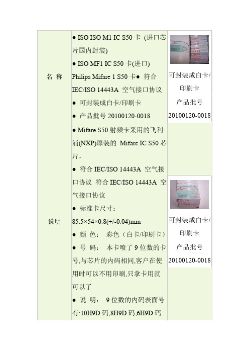
●说明:9位数的内码表面号有:10H9D码,8H9D码,6H9D码.有的客户会指定类型
可封装成白卡/印刷卡
产品批号20100120-0018
产品介绍
● Mifare S50射频卡采用的飞利浦(NXP)原装的Mifare IC S50芯片,符合IEC/ISO 14443A空气接口协议。其具有先进的数据加密及双向密码验证系统,和16个完全独立的扇区,有着极高稳定性和广泛的应用范围,是企业一卡通,水表预付费,公交储值卡,高速公路收费,停车场,小区管理,交运卡,公园,公路等首选的RFID产品。
MF1_S50简介(中文)
数据块可作两种应用:
★用作一般的数据保存,可以进行读、写操作。
★用作数据值,可以进行初始化值、加值、减值、读值操作。
4、每个扇区的块3为控制块,包括了密码A、存取控制、密码B。具体结构如下:
密码A(6字节)存取控制(4字节)密码B(6字节)
5、每个扇区的密码和存取控制都是独立的,可以根据实际需要设定各自的密码及存取控制。存取控制为4个字节,共32位,扇区中的每个块(包括数据块和控制块)的存取条件是由密码和存取控制共同决定的,在存取控制中每个块都有相应的三个控制位,定义如下:
密码B:验证KEYA或KEYB正确后,可读、可写。
三、工作原理
卡片的电气部分只由一个天线和ASIC组成。
天线:卡片的天线是只有几组绕线的线圈,很适于封装到IS0卡片中。
ASIC:卡片的ASIC由一个高速(106KB波特率)的RF接口,一个控制单元和一个
8K位EEPROM组成。
工作原理:读写器向M1卡发一组固定频率的电磁波,卡片内有一个LC串联谐振电路,其频率与读写器发射的频率相同,在电磁波的激励下,LC谐振电路产生共振,从而使电容内有了电荷,在这个电容的另一端,接有一个单向导通的电子泵,将电容内的电荷送到另一个电容内储存,当所积累的电荷达到2V时,此电容可做为电源为其它电路提供工作电压,将卡内数据发射出去或接取读写器的数据。
C11_b
C10_b
字节7
C13
C12
C11
C10
C33_b
C32_b
C31_b
C30_b
字节8
C33
C32
C31
C30
C23
C22
C21
M1卡(S50)资料讲解
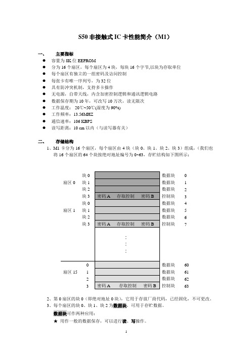
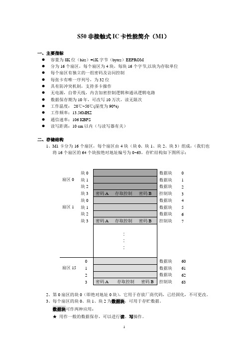
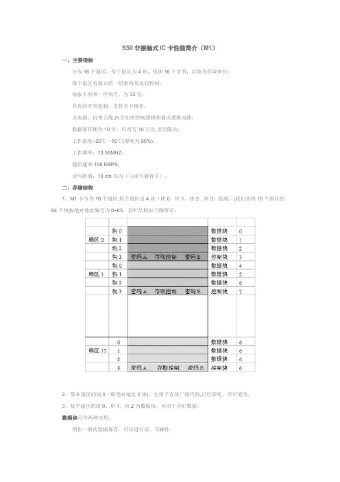
S50非接触式IC卡性能简介(M1)一、主要指标●容量为8K位EEPROM●分为16个扇区,每个扇区为4块,每块16个字节,以块为存取单位●每个扇区有独立的一组密码及访问控制●每张卡有唯一序列号,为32位●具有防冲突机制,支持多卡操作●无电源,自带天线,内含加密控制逻辑和通讯逻辑电路●数据保存期为10年,可改写10万次,读无限次●工作温度:-20℃~50℃(湿度为90%)●工作频率:13.56MHZ●通信速率:106 KBPS●读写距离:10 cm以内(与读写器有关)二、存储结构1、M1卡分为16个扇区,每个扇区由4块(块0、块1、块2、块3)组成,(我们也将16个扇区的64个块按绝对地址编号为0~63,存贮结构如下图所示:数据块0数据块 1数据块 2控制块 3数据块 4数据块 5数据块 6控制块7数据块60数据块61数据块62控制块632、第0扇区的块0(即绝对地址0块),它用于存放厂商代码,已经固化,不可更改。
3、每个扇区的块0、块1、块2为数据块,可用于存贮数据。
数据块可作两种应用:★用作一般的数据保存,可以进行读、写操作。
★用作数据值,可以进行初始化值、加值、减值、读值操作。
4、每个扇区的块3为控制块,包括了密码A、存取控制、密码B。
具体结构如下:密码A(6字节)存取控制(4字节)密码B(6字节)5、每个扇区的密码和存取控制都是独立的,可以根据实际需要设定各自的密码及存取控制。
存取控制为4个字节,共32位,扇区中的每个块(包括数据块和控制块)的存取条件是由密码和存取控制共同决定的,在存取控制中每个块都有相应的三个控制位,定义如下:块0:C10 C20 C30块1:C11 C21 C31块2:C12 C22 C32块3:C13 C23 C33三个控制位以正和反两种形式存在于存取控制字节中,决定了该块的访问权限(如进行减值操作必须验证KEY A,进行加值操作必须验证KEY B,等等)。
三个控制位在存取控制字节中的位置,以块0为例:对块0的控制:字节7字节8字节9( 注:C10_b表示C10取反)存取控制(4字节,其中字节9为备用字节)结构如下所示:字节6字节7字节8字节9( 注:_b表示取反)6、数据块(块0、块1、块2)的存取控制如下:(KeyA|B 表示密码A或密码B,Never表示任何条件下不能实现)例如:当块0的存取控制位C10 C20 C30=1 0 0时,验证密码A或密码B正确后可读;验证密码B正确后可写;不能进行加值、减值操作。
mifare s50s70 到plus cpu卡升级方案
2.3
卡片存在的安全隐患............................................................................................... 3
3. “破解门”应对策略 ...........................................................................................4
2.2 存在安全隐患的卡片
存在安全隐患的 MIFARE Classic 卡片如表 1 所示:
表1
存在安全隐患的 MIFARE Classic 卡片
卡片型号 MIFARE Mini MIFARE S50 卡 MIFARE S70 卡
卡片容量 320 字节 1Kbyte 4Kbyte
©2009 Guangzhou ZHIYUAN Electronics CO., LTD. 2
©2009 Guangzhou ZHIYUAN Electronics CO., LTD.
5
广州致远电子有限公司
MIFARE S50/S70 到 PLUS CPU 卡升级方案
卡片升级方案
l 安全性:通过 EAL 4+认证; l 序列号:4 或 7 字节可设,支持随机识别模式; l 性价比:比其它 CPU 卡片便宜一半。
©2009 Guangzhou ZHIYUAN Electronics CO., LTD. 3
广州致远电子有限公司
MIFARE S50/S70 到 PLUS CPU 卡升级方案
卡片升级方案
3. “破解门”应对策略
首先,我们应该认识到,世界上没有任何一样东西是破解不了的,只不过是破解者所 需要付出的时间与成本是多少而已。同理,对于卡片的破解我们也不需惊慌,应当将其看 作计算机小病毒一样看待,属于普遍的现象。对于病毒的出现原厂必有改良措施及更新“杀 毒软件”来进行应对。只有明与暗不断的博奕,卡片才会更加可靠稳定,我们的社会才会 不断进步与发展。
Mifare1 S50IC卡中文说明书

科技成就梦想 火眼科技S50非接触式IC 卡性能简介(M1)一、 主要指标容量为8K 位EEPROM分为16个扇区,每个扇区为4块,每块16个字节,以块为存取单位 每个扇区有独立的一组密码及访问控制 每张卡有唯一序列号,为32位 具有防冲突机制,支持多卡操作无电源,自带天线,内含加密控制逻辑和通讯逻辑电路 数据保存期为10年,可改写10万次,读无限次 工作温度:-20℃~50℃(湿度为90%) 工作频率:13.56MHZ 通信速率:106 KBPS读写距离:10 cm 以内(与读写器有关)二、 存储结构1、M1卡分为16个扇区,每个扇区由4块(块0、块1、块2、块3)组成,(我们也将16个扇区的64个块按绝对地址编号为0~63,存贮结构如下图所示:块0 数据块 0 扇区0 块1数据块 1 块2数据块 2 块3 密码A 存取控制 密码B 控制块 3 块0 数据块 4 扇区1 块1 数据块 5 块2数据块 6 块3 密码A 存取控制 密码B 控制块 7∶ ∶ ∶0 数据块 60 扇区15 1数据块 61 2数据块 623密码A 存取控制 密码B控制块632、第0扇区的块0(即绝对地址0块),它用于存放厂商代码,已经固化,不可更改。
3、每个扇区的块0、块1、块2为数据块,可用于存贮数据。
Edited by Foxit ReaderCopyright(C) by Foxit Software Company,2005-2008For Evaluation Only.数据块可作两种应用:★ 用作一般的数据保存,可以进行读、写操作。
★ 用作数据值,可以进行初始化值、加值、减值、读值操作。
4、每个扇区的块3为控制块,包括了密码A、存取控制、密码B。
具体结构如下:密码A(6字节)存取控制(4字节)密码B(6字节)5、每个扇区的密码和存取控制都是独立的,可以根据实际需要设定各自的密码及存取控制。
存取控制为4个字节,共32位,扇区中的每个块(包括数据块和控制块)的存取条件是由密码和存取控制共同决定的,在存取控制中每个块都有相应的三个控制位,定义如下:块0: C10 C20 C30块1: C11 C21 C31块2: C12 C22 C32块3: C13 C23 C33三个控制位以正和反两种形式存在于存取控制字节中,决定了该块的访问权限(如进行减值操作必须验证KEY A,进行加值操作必须验证KEY B,等等)。
一卡通系统的安全评估
Micr ocomputer Applica tions V ol.27,No.1,2011研究与设计微型电脑应用2011年第27卷第1期3文章编号:1007-757X(2011)02-0032-02一卡通系统的安全评估蔡秋亮摘要:介绍了Mifare Classic 非接触智能卡的安全性,分析了一卡通系统的安全性主要依赖的因素,就目前使用的一卡通系统安全机制作出评估。
最后就Mifare Classic 卡可能存在的风险,建议一卡通系统用户逐步升级采用CPU 卡。
关键词:Mifare ;安全;一卡通中图分类号:TP311文献标志码:A0引言日前,IC 卡行业内公布了一则关于IC 卡存在严重安全漏洞,Mifare Classic RFID 芯片算法被攻破的消息。
此消息已在各IC 卡应用单位引发了较大的震动,也引起了业内对IC 卡一卡通系统安全性的讨论。
1Mifare Classic 卡Mifare Classic 卡(Mifare S50和Mifare S70卡)的是NXP (前身是飞利浦半导体)提供的逻辑加密卡芯片。
此类卡片以其较低的价格、较灵活的应用、较高的安全性(未被攻破之前的预期)的优势,使其在国内的小额支付、身份识别领域具有广泛的应用,全球的发卡量估计在10亿以上。
[1]1.1Mifare Classic 的应用安全性Mifare 卡自身的安全性主要体现在如下方面:每张卡有唯一序列号,为32位每个扇区(Section )有独立的一组(2条)密码及访问控制采用Challenge-Response 方式3重认证小额支付类应用系统的安全性,主要依赖于读取卡片内部数据并核实其合法性以及受控的数据更新。
身份识别类应用系统的安全性,主要依赖于卡的32位唯一序列号。
1.2Mifare Classic 的安全攻击Mifare Classic 的安全性自2004年开始受到了来自各方面的挑战。
2004年:国内的芯片商以硬件的方式复制了MifareClassic 卡2007年11月:Verdult &De Koning Gans (俄罗斯):研制成功ISO 14443A 侦听和攻击设备(Ghost &Proxmark )2008年2月:Verdult (俄罗斯):成功复制了MifareUltralight 卡2008年3月:Digital Security (俄罗斯):完成了全部Mifare Classic 芯片的反向工程2008年10月:Digital Security (RU):将Mifare Classic芯片的攻击技术发表在ESORICS 2008年刊1.3攻破后可能出现的风险1.3.1伪造卡的出现原Mifare Classic 卡片由于其加密算法的保密和32bit 的UID (全球唯一代码)的限制,伪卡的制作具有相当难度,一般依赖于具有Mifare Classic 卡生产能力的卡商。
M1-S50非接触式IC卡性能简介
S50非接触式IC卡性能简介(M1)一、主要指标分为16个扇区,每个扇区为4块,每块16个字节,以块为存取单位;每个扇区有独立的一组密码及访问控制;每张卡有唯一序列号,为32位;具有防冲突机制,支持多卡操作;无电源,自带天线,内含加密控制逻辑和通讯逻辑电路;数据保存期为10年,可改写10万次,读无限次;工作温度:-20℃~50℃(湿度为90%);工作频率:13.56MHZ;通信速率:106 KBPS;读写距离:10 cm以内(与读写器有关)。
二、存储结构1、M1卡分为16个扇区,每个扇区由4块(块0、块1、块2、块3)组成,(我们也将16个扇区的64个块按绝对地址编号为0~63,存贮结构如下图所示:2、第0扇区的块0(即绝对地址0块),它用于存放厂商代码,已经固化,不可更改。
3、每个扇区的块0、块1、块2为数据块,可用于存贮数据。
数据块可作两种应用:用作一般的数据保存,可以进行读、写操作。
用作数据值,可以进行初始化值、加值、减值、读值操作。
4、每个扇区的块3为控制块,包括了密码A、存取控制、密码B。
具体结构如下:5、每个扇区的密码和存取控制都是独立的,可以根据实际需要设定各自的密码及存取控制。
存取控制为4个字节,共32位,扇区中的每个块(包括数据块和控制块)的存取条件是由密码和存取控制共同决定的,在存取控制中每个块都有相应的三个控制位,定义如下:三个控制位以正和反两种形式存在于存取控制字节中,决定了该块的访问权限(如进行减值操作必须验证KEY A,进行加值操作必须验证KEY B,等等)。
三个控制位在存取控制字节中的位置,以块0为例:对块0的控制:存取控制(4字节,其中字节9为备用字节)结构如下所示:6、数据块(块0、块1、块2)的存取控制如下:例如:当块0的存取控制位C10 C20 C30=1 0 0时,验证密码A或密码B正确后可读;验证密码B正确后可写;不能进行加值、减值操作。
7、控制块块3的存取控制与数据块(块0、1、2)不同,它的存取控制如下:例如:当块3的存取控制位C13 C23 C33=1 0 0时,表示:密码A:不可读,验证KEYA或KEYB正确后,可写(更改);存取控制:验证KEYA或KEYB正确后,可读、可写;密码B:验证KEYA或KEYB正确后,可读、可写。
非接触式IC卡Mifare-S50卡详细介绍
非接触式IC卡Mifare S50卡详细介绍一、何谓RFID与非接触式IC卡(Contactless Samrt Card)RFID (Radio Frequency Identification)常称为感应式电子晶片或近接卡、感应卡、非接触智能卡、非接触IC卡等等。
一套完整RFID系统由Reader 与Transponder两部分组成,其动作原理为由Re ader发射一特定频率之无线电波能量给Transponder,用以驱动Transponder 电路将内部之ID Code送出,此时Reader便接收此ID Code。
Transponder的特殊在于免用电池、免接触、免刷卡故不怕脏污,且晶片密码为世界唯一无法复制COPY,安全性高、长寿命。
RFID的产品有电容式(Capacatine)、微波式(Microwave)、无线电频率RF(R adioFrequency),因电容式在使用时须与CSC验票机几乎贴近才能感应,而微波式则须与CSC验票机直线对准,只有无线电频率式则无此限制,所以目前CSC 的主流卡片是飞利浦的MIFAER卡片,其材质采用无线电频率式;而以无线电频率不含电池之CSC,其动作原理是经由内部RF天线接收由读写器所发送出来之电波,感应出一微小电源电压来供应内部电路及读写器所需之电力,亦藉由此感应电压来读写、运算、储存卡片内记忆体资料或藉由读写器和外界接触,并进行卡片和读写器彼此间之资料之交换;其卡片特性概述如下:1、尺寸:信用卡尺寸86mm*54mm*0.76mm。
2、外型:坚固、防潮、不易弯曲变形。
3、电池:无内部电池。
4、读写距离:与读写单元间距离2-10CM内均可正确读写资料。
5、读写角度:与读写单元上方半球幅度内均可正确读写资料。
6、运输方式:无线电调频通信方式。
7、内部构造:固态电子装置(Solid-state Electric Device),有内藏记忆体、微处理器晶片两种形式。
S50 IC卡
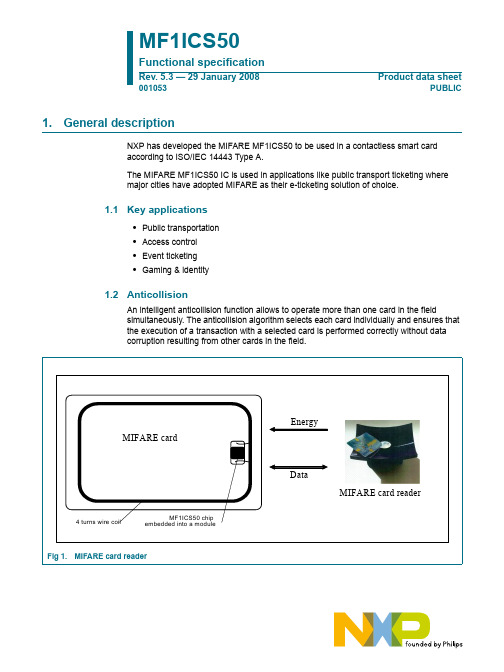
MF1ICS50Functional specificationRev. 5.3 — 29 January 2008Product data sheet001053PUBLIC 1.General descriptionNXP has developed the MIFARE MF1ICS50 to be used in a contactless smart cardaccording to ISO/IEC 14443 Type A.The MIFARE MF1ICS50 IC is used in applications like public transport ticketing wheremajor cities have adopted MIFARE as their e-ticketing solution of choice.1.1Key applications•Public transportation•Access control•Event ticketing•Gaming & identity1.2AnticollisionAn intelligent anticollision function allows to operate more than one card in the fieldsimultaneously. The anticollision algorithm selects each card individually and ensures thatthe execution of a transaction with a selected card is performed correctly without datacorruption resulting from other cards in the field.MIFARE card reader1.3Simple integration and user convenienceThe MF1ICS50 is designed for simple integration and user convenience. Which couldallow complete ticketing transactions to be handled in less than 100 ms. Thus, theMF1ICS50card user is not forced to stop at the reader leading to a high throughput atgates and reduced boarding times onto busses. The MIFARE card may also remain in thewallet during the transaction, even if there are coins in it.1.4SecuritySeveral security measures like mutual challenge and response authentication, dataciphering and message authentication checks support the protection of the systemagainst various attack scenarios. The UID of the IC as a base of key diversificationsupports the security concept.1.5Delivery options•Die on wafer•Bumped die on wafer•MOA4 or MOA2 contactless card module•Flip chip package2.Features2.1MIFARE‚ RF Interface (ISO/IEC 14443 A)Contactless transmission of data and supply energy (no battery needed)Operating distance: Up to 100mm (depending on antenna geometry)Operating frequency: 13.56 MHzData transfer: 106 kbit/sData integrity: 16 Bit CRC, parity, bit coding, bit countingAnticollisionTypical ticketing transaction: < 100 ms (including backup management)2.2EEPROM1 Kbyte, organized in 16 sectors with 4 blocks of 16 bytes each (one block consists of16 byte)User definable access conditions for each memory blockData retention of 10 years.Write endurance 100.000 cycles2.3SecurityMutual three pass authentication (ISO/IEC DIS 9798-2)Individual set of two keys per sector (per application) to support multi-application with key hierarchyUnique serial number for each device3.Ordering informationSee Delivery Type Addendum of Device 4.Block diagram5.Pinning information5.1PinningSee Delivery Type Addendum of Device6.Functional description6.1Block descriptionThe MF1ICS50 chip consists of the 1 Kbyte EEPROM, the RF-Interface and the DigitalControl Unit. Energy and data are transferred via an antenna, which consists of a coil witha few turns directly connected to the MF1ICS50. No further external components arenecessary. (For details on antenna design please refer to the document MIFARE‚ Card ICCoil Design Guide.)•RF-Interface:–Modulator/Demodulator–Rectifier–Clock Regenerator–Power On Reset–Voltage Regulator•Anticollision: Several cards in the field may be selected and operated in sequence•Authentication: Preceding any memory operation the authentication procedureensures that access to a block is only possible via the two keys specified for eachblock•Control & Arithmetic Logic Unit: Values are stored in a special redundant format and can be incremented and decremented•EEPROM-Interface•Crypto unit: The CRYPTO1 stream cipher of the MF1ICS50 is used for authentication and enchryption of data exchange.•EEPROM: 1 Kbyte is organized in 16 sectors with 4 blocks each. A block contains16bytes. The last block of each sector is called “trailer”, which contains two secretkeys and programmable access conditions for each block in this sector.6.2Communication principleThe commands are initiated by the reader and controlled by the Digital Control Unit of theMF1ICS50 according to the access conditions valid for the corresponding sector.6.2.1Request standard/ allAfter Power On Reset (POR) of a card it can answer to a request command - sent by thereader to all cards in the antenna field - by sending the answer to request code (ATQAaccording to ISO/IEC 14443A).6.2.2Anticollision loopIn the anticollision loop the serial number of a card is read. If there are several cards in theoperating range of the reader, they can be distinguished by their unique serial numbersand one can be selected (select card) for further transactions. The unselected cardsreturn to the standby mode and wait for a new request command.6.2.3Select cardWith the select card command the reader selects one individual card for authenticationand memory related operations. The card returns the Answer To Select (ATS) code(= 08h), which determines the type of the selected card. Please refer to the documentMIFARE‚Standardized Card Type Identification Procedure for further details.6.2.4Three pass authenticationAfter selection of a card the reader specifies the memory location of the following memory access and uses the corresponding key for the three pass authentication procedure. Aftera successful authentication all memory operations are encrypted.6.2.5Memory operationsAfter authentication any of the following operations may be performed:•Read block•Write block•Decrement: Decrements the contents of a block and stores the result in a temporary internal data-register•Increment: Increments the contents of a block and stores the result in the data-register•Restore: Moves the contents of a block into the data-register•Transfer: Writes the contents of the temporary internal data-register to a value block6.3Data integrityFollowing mechanisms are implemented in the contactless communication link between reader and card to ensure very reliable data transmission:•16 bits CRC per block•Parity bits for each byte•Bit count checking•Bit coding to distinguish between "1", "0", and no information•Channel monitoring (protocol sequence and bit stream analysis)6.4Three pass authentication sequence1.The reader specifies the sector to be accessed and chooses key A or B.2.The card reads the secret key and the access conditions from the sector trailer. Thenthe card sends a random number as the challenge to the reader (pass one).3.The reader calculates the response using the secret key and additional input. Theresponse, together with a random challenge from the reader, is then transmitted to thecard (pass two).4.The card verifies the response of the reader by comparing it with its own challengeand then it calculates the response to the challenge and transmits it (pass three).5.The reader verifies the response of the card by comparing it to its own challenge.After transmission of the first random challenge the communication between card andreader is encrypted.6.5RF interfaceThe RF-interface is according to the standard for contactless smart cardsISO/IEC14443A.The carrier field from the reader is always present (with short pauses when transmitting), because it is used for the power supply of the card.For both directions of data communication there is only one start bit at the beginning of each frame. Each byte is transmitted with a parity bit (odd parity) at the end. The LSB of the byte with the lowest address of the selected block is transmitted first. The maximum frame length is 163 bits (16 data bytes + 2 CRC bytes = 16 * 9 + 2 * 9 + 1 start bit).6.6Memory organizationThe 1024 x 8 bit EEPROM memory is organized in 16 sectors with 4 blocks of 16 bytes each. In the erased state the EEPROM cells are read as a logical “0”, in the written state as a logical “1”.6.6.1Manufacturer blockThis is the first data block (block 0) of the first sector (sector 0). It contains the ICmanufacturer data. Due to security and system requirements this block is write protected after having been programmed by the IC manufacturer at production.6.6.2Data blocksAll sectors contain 3 blocks of 16 bytes for storing data (Sector 0 contains only two datablocks and the read-only manufacturer block).The data blocks can be configured by the access bits as•read/write blocks for e.g. contactless access control or•value blocks for e.g. electronic purse applications, where additional commands like increment and decrement for direct control of the stored value are provided.An authentication command has to be carried out before any memory operation in order to allow further commands.6.6.2.1Value BlocksThe value blocks allow to perform electronic purse functions (valid commands: read, write, increment, decrement, restore, transfer).The value blocks have a fixed data format which permits error detection and correction and a backup management.A value block can only be generated through a write operation in the value block format:•Value: Signifies a signed 4-byte value. The lowest significant byte of a value is stored in the lowest address byte. Negative values are stored in standard 2´s complementformat. For reasons of data integrity and security, a value is stored three times, twicenon-inverted and once inverted.•Adr: Signifies a 1-byte address, which can be used to save the storage address of a block, when implementing a powerful backup management. The address byte isstored four times, twice inverted and non-inverted. During increment, decrement,restore and transfer operations the address remains unchanged. It can only bealtered via a write command.6.6.3Sector trailer (block 3)Each sector has a sector trailer containing the•secret keys A and B (optional), which return logical “0”s when read and•the access conditions for the four blocks of that sector, which are stored in bytes 6...9.The access bits also specify the type (read/write or value) of the data blocks.If key B is not needed, the last 6 bytes of block 3 can be used as data bytes.Byte 9 of the sector trailer is available for user data. For this byte apply the same access rights as for byte 6, 7 and 8.6.7Memory accessBefore any memory operation can be carried out, the card has to be selected andauthenticated as described previously.The possible memory operations for an addressed block depend on the key used and the access conditions stored in the associated sector trailer.Table 1.Memory operationsOperation Description Valid for Block TypeRead reads one memory block read/write, value and sectortrailerWrite writes one memory block read/write, value and sectortrailervalueIncrement increments the contents of ablock and stores the result inthe internal data registervalueDecrement decrements the contents of ablock and stores the result inthe internal data registervalueTransfer writes the contents of theinternal data register to a blockRestore reads the contents of a blockvalueinto the internal data register6.7.1Access conditionsThe access conditions for every data block and sector trailer are defined by 3 bits, whichare stored non-inverted and inverted in the sector trailer of the specified sector.The access bits control the rights of memory access using the secret keys A and B. Theaccess conditions may be altered, provided one knows the relevant key and the currentaccess condition allows this operation.Remark: With each memory access the internal logic verifies the format of the accessconditions. If it detects a format violation the whole sector is irreversible blocked.Remark: In the following description the access bits are mentioned in the non-invertedmode only.The internal logic of the MF1ICS50 ensures that the commands are executed only after anauthentication procedure or never.Table 2.Access conditionsAccess Bits Valid Commands Block DescriptionC13 C23 C33read, write→3sector trailer→2data blockC12 C22 C32read, write, increment, decrement,transfer, restore→1data blockC11 C21 C31read, write, increment, decrement,transfer, restoreC10 C20 C30read, write, increment, decrement,→0data blocktransfer, restoreFig 9.Access conditions6.7.2Access conditions for the sector trailerDepending on the access bits for the sector trailer (block 3) the read/write access to the keys and the access bits is specified as ‘never’, ‘key A’, ‘key B’ or key A|B’ (key A or key B).On chip delivery the access conditions for the sector trailers and key A are predefined as transport configuration. Since key B may be read in transport configuration, new cards must be authenticated with key A. Since the access bits themselves can also be blocked, special care should be taken during personalization of cards.Remark: the grey marked lines are access conditions where key B is readable and may be used for data.Table 3.Access conditions for the sector trailerAccess bits Access condition for RemarkKEYAAccess bitsKEYB C1C2C3read write read write read write 000never key A key A never key A key A Key B may be read 010never never key A never key A never Key B may be read100never key B key A|B never never key B 110never never key A|B never never never 001never key A key A key A key A key A Key B may be read,transport configuration 011never key B key A|B key B never key B 101never never key A|B key B never never 111neverneverkey A|Bnevernevernever6.7.3Access conditions for data blocksDepending on the access bits for data blocks (blocks 0...2) the read/write access isspecified as ‘never’, ‘key A’, ‘key B’ or ‘key A|B’ (key A or key B). The setting of therelevant access bits defines the application and the corresponding applicable commands.•Read/write block: The operations read and write are allowed.•Value block: Allows the additional value operations increment, decrement, transfer and restore. In one case (‘001’) only read and decrement are possible for anon-rechargeable card. In the other case (‘110’) recharging is possible by using key B.•Manufacturer block: The read-only condition is not affected by the access bits setting!•Key management: In transport configuration key A must be used for authentication1Table 4.Access conditions for data blocksAccess bits Access condition for ApplicationC1C2C3read write increment decrement,transfer,restore000key A|B[1]key A|B1key A|B1key A|B1transportconfiguration 010key A|B[1]never never never read/write block100key A|B[1]key B1never never read/write block110key A|B[1]key B1key B1key A|B1value block001key A|B[1]never never key A|B1value block011key B[1]key B1never never read/write block101key B[1]never never never read/write block111never never never never read/write block[1]if Key B may be read in the corresponding Sector Trailer it cannot serve for authentication (all grey markedlines in previous table). Consequences: If the reader tries to authenticate any block of a sector with key Busing grey marked access conditions, the card will refuse any subsequent memory access afterauthentication.1.If Key B may be read in the corresponding Sector Trailer it cannot serve for authentication (all grey marked lines in previous table). Consequences: If the RDW tries to authenticate any block of a sector with key B using grey marked access conditions, the card will refuse any subsequent access after authentication.7.Limiting valuesSee Delivery Type Addendum of Device 8.Recommended operating conditionsSee Delivery Type Addendum of Device 9.CharacteristicsSee Delivery Type Addendum of Device 10.Support informationFor additional information, please visit: 11.Package outlineSee Delivery Type Addendum of Device12.Revision historyTable 5.Revision historyDocument ID Release date Data sheet status Change notice Supersedes 00105329 January 2008Product data sheet 5.2 Modifications:•Update•General rewording of MIFARE designation and commercialconditions00105215 January 2007Product data sheet 5.1 Modifications:•The format of this data sheet has been redesigned to comply with the new identityguidelines of NXP Semiconductors.•Legal texts have been adapted to the new company name.13.Legal information13.1Data sheet status[1]Please consult the most recently issued document before initiating or completing a design. [2]The term ‘short data sheet’ is explained in section “Definitions”.[3]The product status of device(s) described in this document may have changed since this document was published and may differ in case of multiple devices. The latest product status information is available on the Internet at URL .13.2DefinitionsDraft — The document is a draft version only. The content is still under internal review and subject to formal approval, which may result in modifications or additions. NXP Semiconductors does not give any representations or warranties as to the accuracy or completeness ofinformation included herein and shall have no liability for the consequences of use of such information.Short data sheet — A short data sheet is an extract from a full data sheet with the same product type number(s) and title. A short data sheet is intended for quick reference only and should not be relied upon to contain detailed and full information. For detailed and full information see the relevant full data sheet, which is available on request via the local NXP Semiconductors sales office. In case of any inconsistency or conflict with the short data sheet, the full data sheet shall prevail.13.3DisclaimersGeneral — Information in this document is believed to be accurate andreliable. However, NXP Semiconductors does not give any representations or warranties, expressed or implied, as to the accuracy or completeness of such information and shall have no liability for the consequences of use of such information.Right to make changes — NXP Semiconductors reserves the right to make changes to information published in this document, including withoutlimitation specifications and product descriptions, at any time and without notice. This document supersedes and replaces all information supplied prior to the publication hereof.Suitability for use — NXP Semiconductors products are not designed, authorized or warranted to be suitable for use in medical, military, aircraft, space or life support equipment, nor in applications where failure ormalfunction of a NXP Semiconductors product can reasonably be expected toresult in personal injury, death or severe property or environmental damage. NXP Semiconductors accepts no liability for inclusion and/or use of NXP Semiconductors products in such equipment or applications and therefore such inclusion and/or use is at the customer’s own risk.Applications — Applications that are described herein for any of these products are for illustrative purposes only. NXP Semiconductors makes no representation or warranty that such applications will be suitable for the specified use without further testing or modification.Limiting values — Stress above one or more limiting values (as defined in the Absolute Maximum Ratings System of IEC 60134) may cause permanent damage to the device. Limiting values are stress ratings only and operation of the device at these or any other conditions above those given in theCharacteristics sections of this document is not implied. Exposure to limiting values for extended periods may affect device reliability.Terms and conditions of sale — NXP Semiconductors products are sold subject to the general terms and conditions of commercial sale, as published at /profile/terms , including those pertaining to warranty, intellectual property rights infringement and limitation of liability, unlessexplicitly otherwise agreed to in writing by NXP Semiconductors. In case of any inconsistency or conflict between information in this document and such terms and conditions, the latter will prevail.No offer to sell or license — Nothing in this document may be interpreted or construed as an offer to sell products that is open for acceptance or the grant, conveyance or implication of any license under any copyrights, patents or other industrial or intellectual property rights.13.4TrademarksNotice: All referenced brands, product names, service names and trademarks are the property of their respective owners.MIFARE — is a trademark of NXP B.V.14.Contact informationFor additional information, please visit: For sales office addresses, send an email to: salesaddresses@Document status [1][2]Product status [3]DefinitionObjective [short] data sheet Development This document contains data from the objective specification for product development. Preliminary [short] data sheet Qualification This document contains data from the preliminary specification. Product [short] data sheetProductionThis document contains the product specification.15.TablesTable 1.Memory operations. . . . . . . . . . . . . . . . . . . . . .11 Table 2.Access conditions. . . . . . . . . . . . . . . . . . . . . . .12 Table 3.Access conditions for the sector trailer. . . . . .13Table 4.Access conditions for data blocks . . . . . . . . . .14 Table 5.Revision history. . . . . . . . . . . . . . . . . . . . . . . .1616.FiguresFig 1.MIFARE card reader . . . . . . . . . . . . . . . . . . . . . . .1Fig 2.Block diagram . . . . . . . . . . . . . . . . . . . . . . . . . . . .3Fig 3.Three pass authentication . . . . . . . . . . . . . . . . . . .5Fig 4.Memory organization. . . . . . . . . . . . . . . . . . . . . . .7Fig 5.Manufacturer block . . . . . . . . . . . . . . . . . . . . . . . .8Fig 6.Value blocks. . . . . . . . . . . . . . . . . . . . . . . . . . . . . .9Fig 7.Sector trailer . . . . . . . . . . . . . . . . . . . . . . . . . . . . .9Fig 8.Memory access . . . . . . . . . . . . . . . . . . . . . . . . . .10Fig 9.Access conditions . . . . . . . . . . . . . . . . . . . . . . . .12continued >>© NXP B.V.2008.All rights reserved.For more information, please visit: For sales office addresses, please send an email to: salesaddresses@Please be aware that important notices concerning this document and the product(s)described herein, have been included in section ‘Legal information’.17.Contents1General description. . . . . . . . . . . . . . . . . . . . . . 11.1Key applications . . . . . . . . . . . . . . . . . . . . . . . . 11.2Anticollision. . . . . . . . . . . . . . . . . . . . . . . . . . . . 11.3Simple integration and user convenience. . . . . 21.4Security. . . . . . . . . . . . . . . . . . . . . . . . . . . . . . . 21.5Delivery options . . . . . . . . . . . . . . . . . . . . . . . . 22Features . . . . . . . . . . . . . . . . . . . . . . . . . . . . . . . 22.1MIFARE‚ RF Interface (ISO/IEC 14443 A) . . . . 22.2EEPROM . . . . . . . . . . . . . . . . . . . . . . . . . . . . . 22.3Security. . . . . . . . . . . . . . . . . . . . . . . . . . . . . . . 23Ordering information. . . . . . . . . . . . . . . . . . . . . 34Block diagram . . . . . . . . . . . . . . . . . . . . . . . . . . 35Pinning information. . . . . . . . . . . . . . . . . . . . . . 35.1Pinning . . . . . . . . . . . . . . . . . . . . . . . . . . . . . . . 36Functional description . . . . . . . . . . . . . . . . . . . 46.1Block description . . . . . . . . . . . . . . . . . . . . . . . 46.2Communication principle . . . . . . . . . . . . . . . . . 46.2.1Request standard/ all . . . . . . . . . . . . . . . . . . . . 46.2.2Anticollision loop. . . . . . . . . . . . . . . . . . . . . . . . 46.2.3Select card . . . . . . . . . . . . . . . . . . . . . . . . . . . . 56.2.4Three pass authentication . . . . . . . . . . . . . . . . 56.2.5Memory operations. . . . . . . . . . . . . . . . . . . . . . 66.3Data integrity. . . . . . . . . . . . . . . . . . . . . . . . . . . 66.4Three pass authentication sequence . . . . . . . . 66.5RF interface . . . . . . . . . . . . . . . . . . . . . . . . . . . 76.6Memory organization . . . . . . . . . . . . . . . . . . . . 76.6.1Manufacturer block. . . . . . . . . . . . . . . . . . . . . . 86.6.2Data blocks. . . . . . . . . . . . . . . . . . . . . . . . . . . . 86.6.2.1Value Blocks. . . . . . . . . . . . . . . . . . . . . . . . . . . 86.6.3Sector trailer (block 3) . . . . . . . . . . . . . . . . . . . 96.7Memory access . . . . . . . . . . . . . . . . . . . . . . . 106.7.1Access conditions. . . . . . . . . . . . . . . . . . . . . . 126.7.2Access conditions for the sector trailer. . . . . . 136.7.3Access conditions for data blocks. . . . . . . . . . 147Limiting values. . . . . . . . . . . . . . . . . . . . . . . . . 158Recommended operating conditions. . . . . . . 159Characteristics. . . . . . . . . . . . . . . . . . . . . . . . . 1510Support information . . . . . . . . . . . . . . . . . . . . 1511Package outline . . . . . . . . . . . . . . . . . . . . . . . . 1512Revision history. . . . . . . . . . . . . . . . . . . . . . . . 1613Legal information. . . . . . . . . . . . . . . . . . . . . . . 1713.1Data sheet status . . . . . . . . . . . . . . . . . . . . . . 1713.2Definitions. . . . . . . . . . . . . . . . . . . . . . . . . . . . 1713.3Disclaimers. . . . . . . . . . . . . . . . . . . . . . . . . . . 1713.4Trademarks. . . . . . . . . . . . . . . . . . . . . . . . . . . 1714Contact information . . . . . . . . . . . . . . . . . . . . 1715Tables. . . . . . . . . . . . . . . . . . . . . . . . . . . . . . . . 1816Figures. . . . . . . . . . . . . . . . . . . . . . . . . . . . . . . 1817Contents. . . . . . . . . . . . . . . . . . . . . . . . . . . . . . 19。
一卡通(S50卡)的序列号存储在哪个扇区的哪个块

⑤ 设备低劣:低劣的设备将直接影响卡的读写性能。对MF卡进行块3编程操作的设备,特别要求其性能必须十分可靠,运行十分稳定!建议选用由飞利浦公司原装读写模块构建的知名读写机具!
3.读UltraLight标签时,请将扇区号设为0,块号即为UltraLight标签对应的页号.读取的内容是从选择的页号开始的连续4个页.
4.写UltraLight标签时,只有低四个字节能被写入标签,余下的12个字节为0;
另外,有专用于UltraLight标签的写命令ULWrite,
知识学习
3)点击“Anticoll”(图2-1中5),Mifare One 防冲突获取射频场中一张Mifare One标签的UID,如果防冲突执行成功,“卡号”文本框将会显示获取到的4字节标签UID(图2-1中13);否则状态栏显示“防冲突失败”。ULAnticoll: UltraLight 防冲突:获取射频场中一张UltraLight标签的UID,如果防冲突执行成功,“卡号”文本框将会显示获取到的7字节标签UID;否则状态栏显示防冲突失败。
2、第0扇区的块0(即绝对地址0块),它用于存放厂商代码,已经固化,不可更改。
3、每个扇区的块0、块1、块2为数据块,可用于存贮数据。
数据块可作两种应用:
★用作一般的数据保存,可以进行读、写操作。
★用作数据值,可以进行初始化值、加值、减值、读值操作。
4、每个扇区的块3为控制块,包括了密钥A、存取控制、密钥B。具体结构为:密钥A(6字节) 存取控制(4字节)密钥B(6字节)
非接触IC卡物理结构(S50)

8
ASCII
30000(小数二位)
25
可改写
8+8
ASCII
30000 20080818
26
可改写
27
密钥区不能存放其它信息
----
-----
7
28
可改写
4
Hex
23600
29
可改写
16
ASCII
20071023
30
可改写
31
密钥区不能存放其它信息
----
-----
8至15扇区同上
----
-----
4
16
可改写
16
ASCII
李四
17
可改写
16
ASCII
王五
18
可改写
16
ASCII
200709---
-----
5
20
可改写
16
ASCII
20070910
21
可改写
16
ASCII
20080823
22
可改写
23
密钥区不能存放其它信息
----
-----
6
24
一、
Mifare卡(M1卡)是非接触式IC卡的一种,全称Mifare One ,一般是S50的MF卡,卡总大小为1K字节,S70为2K字节,等等还有更大的容量。下面是S50卡的物理结构:
扇区号
块号
字段名
长度
编码
数据模拟
0
0
卡出厂信息不能改写
前四字节为卡号
1
可改写
16
ASCII
(可自定义)
1号卡
各种非接触卡简介

各种非接触卡简介概述:为了线下商盟用户识别与消费的考虑,下面研究一下各种非接触式卡技术。
谈到非接首先了解一下RFID。
(Radio Frequency Identification)射频身份识别,RFID标签芯片的内部结构主要包括射频前端、模拟前端、数字基带处理单元和EEPROM存储单元四部分。
根据电感耦合原理在标签天线两端产生感应电势差,形成微弱电流,当超过阈值时,激活RFID 电路工作,从而对存储器进行读/写操作。
RFID频率分为低频(LF)、高频(HF)、超高频(UHF)、微波(MW),相对应:低频135KHz以下、高频13.56MHz、超高频860M~960MHz、微波2.4G。
ID卡,很早的一种射频卡,出厂后便已有了卡号,每张卡的卡号都不一样,该卡号是固定不变、无法加密、无法擦写。
ID卡与磁卡一样,都仅仅使用了“卡的号码”而已,卡内除了卡号外,无任何保密功能,其“卡号”是公开的。
所以说ID卡就是“感应式磁卡”,由于ID卡内无寄存器,用户的权限等系统功能操作要完全依赖于计算机网络平台及数据库的支持。
一般用在门禁或停车场系统用户身份识别。
IC卡,集成电路卡,将一个专用的集成电路芯片镶嵌于标准的PVC(或ABS等)塑料基片中。
若按接口方式可分为:接触式IC卡:读写设备触点与IC卡触点接触后进行数据的读写。
非接触式IC卡:与IC卡设备无电路接触,而是通过非接触式的读写技术进行读写。
双界面卡:将接触式IC卡与非接触式IC卡组合到一张卡片中,操作独立,(但可以共用CPU 和存储空间)。
主流可按芯片划分:存储卡:卡内集成可编程只读存储器EEPROM,只有数据存储功能,没有数据处理能力。
该卡本身不提供硬件加密功能,只能存储通过系统加密的数据,容易被破解。
逻辑加密卡:卡内集成加密逻辑电路和EEPROM,加密逻辑电路在一定程度上保护卡内数据安全,但层次较低,无法防止恶意攻击。
CPU卡(智能卡):卡内集成中央处理器CPU、EEPROM、随机存储器RAM、固化的卡内操作系统COS(Chip Operating System)和只读存储器ROM。
S50简介
非接触式IC卡与读写器之间无机械接触,避免了因接触读写而产生的各种故障(例如:由于粗暴插卡、非卡外物插入、灰尘或油污导致接触不良造成的故障)。此外,非接触式卡表面无裸露芯片,无须担心芯片脱落、静电击穿、弯曲损坏等问题,既便于卡片印刷,又提高了卡片的使用可靠性。
⑵操作方便
由于非接触通讯,读写器在10CM范围内就可以对卡片操作,所以不必插拨卡,非常方便用户使用。非接触式卡使用时没有方向性,卡片可以在任意方向掠过读写器表面,即可完成操作,这大大提高了每次使用的速度。
M1卡有16个区,每个区都有独立的两组密码KeyA/KeyB和区读写控制位,每个区互不相关.
在M1卡出厂时,KeyA/KeyB默认的密码都是12个F.
密码的验证是在卡内部进行的,读写器只负责给卡提供电并和卡通讯,读写器发送加密的密码到卡,卡内部进行解密验证并发返回值,读写器根据卡的返回值来判断验证是否通过.
名称
● ISOISO M1 IC S50卡(进口芯片国内封装)
●ISO MF1 IC S50卡(进口) Philips Mifare 1 S50卡●符合IEC/ISO 14443A空气接口协议
●可封装成白卡/印刷卡
●产品批号20100120-0018
Mifare 1 非接触式IC智能
Mifare 1 非接触式IC智能(射频)卡一.Mifare 1非接触式IC智能射频卡特点Mifare 1 IC智能(射频)卡的核心是Philips 公司的Mifare 1 IC S50(-01,-02,-03,-04)系列微模块(微晶片)。
它确定了卡片的特性以及卡片读写器的诸多性能。
Mifare 1 IC智能(射频)卡采用先进的芯片制造工艺制作。
内建有高速的CMOS EEPROM,MCU等。
卡片上除了IC微晶片及一副高效率天线外,无任何其他元件。
卡片上无源(无任何电池),工作时的电源能量由卡片读写器天线发送无线电载波信号耦合到卡片上天线而产生电能,一般可达2V以上,供卡片上IC工作。
工作频率13.56MHZ。
Mifare 1射频卡所具有的独特的MIFARE RF(射频)非接触式接口标准已被制定为国际标准:ISO/IEC 14443 TYPE A 标准。
射频卡标准操作距离为100mm(由MCM500 作为读写器核心模块)和25 mm (由MCM200 作为读写器核心模块)。
与卡片读写器的通信速率高达106Kbit/s。
Mifare 1 IC智能(射频)卡上具有先进的数据通信加密并双向验证密码系统;且具有防重叠功能:能在同一时间处理重叠在卡片读写器天线的有效工作距离内的多张重叠的卡片。
Mifare 1 IC智能(射频)卡与读写器通信使用握手式半双工通信协议;卡片上有高速的CRC 协处理器,符合CCITT标准。
卡片制造时具有唯一的卡片系列号,没有重复的相同的两张MIFARE 卡片。
卡片上内建8K(bit)EEPROM存储容量并划分为16个扇区,每个扇区划分为4个数据存储块,每个扇区可由多种方式的密码管理。
卡片上还内建有增值/减值的专项的数学运算电路,非常适合公交/地铁等行业的检票/收费系统。
典型的检票交易时间最长不超过100ms(0.1秒)(包括卡片的认证,6个扇区的读(768bit,2个扇区的认证),2个扇区的写操作(256bit))。
mifireone射频卡基础知识

Mifare-I射频卡是飞利浦公司研发制定的一套
非接触式射频卡的业界标准。目前飞利浦公 司提供有两种版本,分别为拥有 1 Kbytes EEPROM 的 MIFARE® Standard 与拥有 4 Kbytes EEPROM 的 MIFARE® Standard 4k。
扇区 0
Block 1 Block 2 Block 3 (A密码+存储控制+B密码)
Block 0
Block 1 Block 2 Block 3 (A密码+存储控制+B密码)
扇区 1
……
扇区 n
Block 0 Block 1
Block 2
Block 3 (A密码+存储控制+B密码)
扇区15
2、操作权限控制
5、卡操作次数
mifare one卡可以进行超过十万次的写卡操
作,和无限次的读卡操作,对于普通的业 务处理来说完全可以满足需要。但我们在 系统设计中还是要注意系统中业务流程的 合理性,防止过于频繁的读写操作对卡的 影响,造成不必要的卡寿命缩短。例如上 次公司培训时傅老师提到的水控对卡不合 理操作造成影响的案例。
三、Mifare one 卡的操作
1、操作流程
上电复位 复位
以IDLE/ALL模式寻卡
防冲突
选卡
改变操作地址
读/写 验证密码 减值操作 增值操作,等
中止 (完成所有操作)
2、IDLE/ALL寻卡模式
以IDLE模式下寻卡,只有当前感应区只有
IDLE状态的卡片会响应读写卡设备的命令。 而以ALL模式寻卡,则感应区内IDLE和 HALT模式的卡片都会相应读写卡设备的命 令。当某张卡片状态被改变成HALT状态, 如果以IDLE模式寻卡并需要对该卡片进行 操作,则必须将该卡片移开感应区并再次 放入感应区才能寻到该卡片。
RFID门禁实验
RFID门禁实验RFID套件介绍RFID(Radio Frequency Identification),也称为射频识别,是一种通信技术。
它可以通过无线电信号识别特定目标并读取和写入数据,而无需在识别系统和特定目标之间建立机械或光学接触。
射频一般为微波,1-100GHz,适合短距离识别通信。
RFID读写器也分为移动和固定类型。
目前RFID技术应用广泛,如:图书馆,门禁系统,食品安全可追溯性等。
RFID套件组件S50 IC卡(应答器):S50是飞利浦PHILIPS下属子公司恩智浦NXP出品的NXP Mifare1系列芯片型号。
封装这种芯片的卡类,称为S50卡。
S50卡属于非接触式IC卡,其芯片和感应天线无裸露部分,通过无线电波来完成与读卡器之间的读写操作。
它由天线,耦合元件和芯片组成。
通常,发送应答器看起来像标签,每个标签都有一个独特的电子代码,通过将它们附加在它们上来识别对象。
卡进入读写器的射频范围时,接收到读写器发出的电源信号,通过L/C串联谐振电路产生谐振,产生电荷来供给芯片工作,以完成数据的接收、读取、修改、储存、发送等操作。
存储容量:S50:8Kbit,16个分区,每分区两组密码工作频率:13.56 MHz通讯速率:106KBoud读写距离:2.5~10 CMIC钥匙扣卡(S50复旦卡):读卡器:RC522是应用于13.56MHz非接触式通信中高集成度的读写卡芯片,是NXP公司针对“三表”应用推出的一款低电压、低成本、体积小的非接触式读写卡芯片,是智能仪表和便携式手持设备研发的较好选择。
MF RC522利用了先进的调制和解调概念,完全集成了在13.56MHz下所有类型的被动非接触式通信方式和协议。
支持14443A兼容应答器信号。
数字部分处理ISO14443A帧和错误检测。
此外,还支持快速CRYPTO1加密算法,用语验证MIFARE系列产品。
MFRC522支持MIFARE 系列更高速的非接触式通信,双向数据传输速率高达424kbit/s。
非接触式IC卡Mifare S50卡详细介绍

非接触式IC卡Mifare S50卡详细介绍一、何谓RFID与非接触式IC卡(Contactless Samrt Card)RFID (Radio Frequency Identification)常称为感应式电子晶片或近接卡、感应卡、非接触智能卡、非接触IC卡等等。
一套完整RFID系统由Reader 与Transponder两部分组成,其动作原理为由Re ader发射一特定频率之无线电波能量给Transponder,用以驱动Transponder 电路将内部之ID Code送出,此时Reader便接收此ID Code。
Transponder的特殊在于免用电池、免接触、免刷卡故不怕脏污,且晶片密码为世界唯一无法复制COPY,安全性高、长寿命。
RFID的产品有电容式(Capacatine)、微波式(Microwave)、无线电频率RF(R adioFrequency),因电容式在使用时须与CSC验票机几乎贴近才能感应,而微波式则须与CSC验票机直线对准,只有无线电频率式则无此限制,所以目前CSC 的主流卡片是飞利浦的MIFAER卡片,其材质采用无线电频率式;而以无线电频率不含电池之CSC,其动作原理是经由内部RF天线接收由读写器所发送出来之电波,感应出一微小电源电压来供应内部电路及读写器所需之电力,亦藉由此感应电压来读写、运算、储存卡片内记忆体资料或藉由读写器和外界接触,并进行卡片和读写器彼此间之资料之交换;其卡片特性概述如下:1、尺寸:信用卡尺寸86mm*54mm*0.76mm。
2、外型:坚固、防潮、不易弯曲变形。
3、电池:无内部电池。
4、读写距离:与读写单元间距离2-10CM内均可正确读写资料。
5、读写角度:与读写单元上方半球幅度内均可正确读写资料。
6、运输方式:无线电调频通信方式。
7、内部构造:固态电子装置(Solid-state Electric Device),有内藏记忆体、微处理器晶片两种形式。
- 1、下载文档前请自行甄别文档内容的完整性,平台不提供额外的编辑、内容补充、找答案等附加服务。
- 2、"仅部分预览"的文档,不可在线预览部分如存在完整性等问题,可反馈申请退款(可完整预览的文档不适用该条件!)。
- 3、如文档侵犯您的权益,请联系客服反馈,我们会尽快为您处理(人工客服工作时间:9:00-18:30)。
飞利蒲 S50卡技术标准
1)主要指标
●容量为8K位EEPROM
●分为16个扇区,每个扇区为4块,每块16个字节,以块为存取单位
●每个扇区有独立的一组密码及访问控制
●每张卡有唯一序列号,为32位
●具有防冲突机制,支持多卡操作
●无电源,自带天线,内含加密控制逻辑和通讯逻辑电路
●数据保存期为10年,可改写10万次,读无限次
●工作温度:-20℃~50℃(湿度为90%)
●工作频率:13.56MHZ
●通信速率:106 KBPS
●读写距离:10CM以内(与读写器有关)
2)协议标准
ISO 14443标准。
3)存储结构
A.MF1 S50卡分为16个扇区,每个扇区由4块(块0、块1、块2、块3)组成,(我们也将16个扇区的64个块按绝对地址编号为0~63,存贮结构如下图所示:
数据块0
数据块 1
数据块 2
控制块 3
数据块 4
数据块 5
数据块 6
控制块7
数据块60
数据块61
数据块62
控制块63
B.第0扇区的块0(即绝对地址0块),它用于存放厂商代码,已经固化,不可更
改。
C.每个扇区的块0、块1、块2为数据块,可用于存贮数据。
数据块可作两种应用:
★ 用作一般的数据保存,可以进行读、写操作。
★ 用作数据值,可以进行初始化值、加值、减值、读值操作。
D.每个扇区的块3为控制块,包括了密码A 、存取控制、密码B 。
具体结构如下:
密码A (6字节) 存取控制(4字节) 密码B (6字节)
E.每个扇区的密码和存取控制都是独立的,可以根据实际需要设定各自的密码及存取控制。
存取控制为4个字节,共32位,扇区中的每个块(包括数据块和控制块)的存取条件是由密码和存取控制共同决定的,在存取控制中每个块都有相应的三个控制位,定义如下:
块0: C10 C20 C30 块1: C11 C21 C31 块2: C12 C22 C32 块3: C13 C23 C33
三个控制位以正和反两种形式存在于存取控制字节中,决定了该块的访问权限(如进行减值操作必须验证KEY A ,进行加值操作必须验证KEY B ,等等)。
三个控制位在存取控制字节中的位置,以块0为例:
对块0的控制:
字节6 字节7 字节8 字节9
( 注: C10_b 表示C10取反 )
存取控制(4字节,其中字节9为备用字节)结构如下所示:
字节6 字节7 字节8 字节9
( 注: _b表示取反 )
F.数据块(块0、块1、块2)的存取控制如下:
例如:当块0的存取控制位C10 C20 C30=1 0 0时,验证密码A或密码B正确后可读;验证密码B正确后可写;不能进行加值、减值操作。
G.控制块块3的存取控制与数据块(块0、1、2)不同,它的存取控制如下:
例如:当块3的存取控制位C13 C23 C33=1 0 0时,表示:
密码A:不可读,验证KEYA或KEYB正确后,可写(更改)。
存取控制:验证KEYA或KEYB正确后,可读、可写。
密码B:验证KEYA或KEYB正确后,可读、可写。
4)工作原理
卡片的电气部分只由一个天线和ASIC组成。
天线:卡片的天线是只有几组绕线的线圈,很适于封装到IS0卡片中。
ASIC:卡片的ASIC由一个高速(106KB波特率)的RF接口,一个控制单元和一个8K位EEPROM组成。
工作原理:读写器向M1卡发一组固定频率的电磁波,卡片内有一个LC串联谐振
电路,其频率与读写器发射的频率相同,在电磁波的激励下,LC谐振电路产生共振,从而使电容内有了电荷,在这个电容的另一端,接有一个单向导通的电子泵,将电容内的电荷送到另一个电容内储存,当所积累的电荷达到2V时,此电容可做为电源为其它电路提供工作电压,将卡内数据发射出去或接取读写器的数据。
复位应答(Answer to request)
M1射频卡的通讯协议和通讯波特率是定义好的,当有卡片进入读写器的操作范围时,读写器以特定的协议与它通讯,从而确定该卡是否为M1射频卡,即验证卡片的卡型。
防冲突机制 (Anticollision Loop)
当有多张卡进入读写器操作范围时,防冲突机制会从其中选择一张进行操作,未选中的则处于空闲模式等待下一次选卡,该过程会返回被选卡的序列号。
选择卡片(Select Tag)
选择被选中的卡的序列号,并同时返回卡的容量代码。
三次互相确认(3 Pass Authentication)
选定要处理的卡片之后,读写器就确定要访问的扇区号,并对该扇区密码进行密码校验,在三次相互认证之后就可以通过加密流进行通讯。
(在选择另一扇区时,则必须进行另一扇区密码校验。
)
对数据块的操作
读(Read):读一个块;
写(Write):写一个块;
加(Increment):对数值块进行加值;
减(Decrement):对数值块进行减值;
存储(Restore):将块中的内容存到数据寄存器中;
传输(Transfer):将数据寄存器中的内容写入块中;
中止(Halt):将卡置于暂停工作状态;
6)M F1 S50卡修改各区块控制位值和数据
一、08 77 8F 69
(1)以常用设置“08 77 8F 69”控制条件为例,先搞清楚它――具有的访问权限。
1)对“08 77 8F 69”值进行计算,该值定位于各区块3的6、7、8、9四个字节内,字节6=08,字节7=77,字节8=8F,字节9=69(默认值,不予计算)。
2)例如:字节6=08,对应其二进制值=00001000, 则对6、7、8这三个字节进行二进制转换结果见下表:
3)参照表2及表4算法,字节6的全部二进制值取反,字节7的低四位二进制值取反,字节8不变,得到:
4)对以上6、7、8字节的存取/控制二进制已取反值,依照表2、表4块位转换为各块控制值,如下表:
注意: 高4位的各块值=低4位的各块值时,其值可用。
高4位值≠低4位值时,其值不可用!
5)查对访问权限(数据存取控制依照表3,块3存取控制依照表5),该例“08 77 8F 69”的访问权限为:
◆块3 = 011:权限为:KeyA、KeyB均不可读,验证KeyB正确后可改写KeyA和KeyB,验证KeyA或KeyB正确后可读“控制位”。
在此可见密钥KeyB的重要性,KeyB不正确是无法看到块3控制值,更无法修改密钥。
◆块2 = 块1 = 块0 = 110:权限为:验证KeyA或KeyB后可读该块数据、减值以及初始化值,只有验证KeyB 正确后才可改写该块数据,在此可以看到密钥KeyB对改写数据块也起着关键性作用。
(2)“08 77 8F 69”控制条件设置步骤:
由(一)可知:KeyB设置后为不可读,并且改写数据和改写控制位都需要正确验证它,故KeyB设置后程序操作员必须妥善保管KeyB值,否则以后改写数据和控制位时,不正确的KeyB值将无法实现卡的任何操作!!!
1)修改块3控制位的值:最初的各区块3内的KeyA、KeyB都是厂商12个“F”默认值(KeyA在任何条件下均为不可读,大部分读写机程序表现KeyA为未知的12个“0”),在修改控制值时,先不要修改默认密码KeyA和KeyB,在控制位修改成功后,再去更改新密码值。
即先对块3的控制位进行修改(默认值FF 07 80 69改为新值08 77 8F 69)并执行写操作。
控制位写成功后,KeyB亦为12个“0”不可读了,但仍是隐藏的12个“f”默认值。
2)修改块3的KeyA和KeyB值:控制位08 77 8F 69值写成功后,验证KeyB正确后方可改写KeyA和KeyB新密码。
在密码操作模式键入要改写区块之先前密码B(先前密码为默认值时,则不需改动和加载),加载后反回数据操作模式,再进行读值、KeyA 和KeyB值的改写。
3)修改块0~块2中数据:由新的控制条件08778F69可知,要修改数据,必须先验证KeyB,故先设置密码操作为KeyB认证方式,加载后再返回数据操作模式,对要
修改的数据块进行值的改写操作。
4)上例中分析了“08 77 8F 69”的访问条件及其改写步骤,对用户的其它控制条件亦可参照应用。
二、FF 07 80 69
(1)以常用设置“FF 07 80 69”控制条件为例,先搞清楚它――具有的访问权限。
1)对“ff 07 80 69”值进行计算,该值定位于各区块3的6、7、8、9四个字节内,字节6=ff,字节7=07,字节8=80,字节9=69(默认值,不予计算)。
2)例如:字节6=ff,对应其二进制值=11111111, 则对6、7、8这三个字节进行二进制转换结果见下表:
3)参照表2及表4算法,字节6的全部二进制值取反,字节7的低四位二进制值取反,字节8不变,得到:
4)对以上6、7、8字节的存取/控制二进制已取反值,依照表2、表4块位转换为各块控制值,如下表:
注意: 高4位的各块值=低4位的各块值时,其值可用。
高4位值≠低4位值时,
其值不可用!
5)查对访问权限(数据存取控制依照表3,块3存取控制依照表5),该例“08 77 8F 69”的访问权限为:
◆块3 = 001:权限为:KeyA不可读,验证KeyA或KeyB正确后可改写KeyA和KeyB,验证KeyA或KeyB正确后可读写“控制位”。
◆块2 = 块1 = 块0 = 000:权限为:验证KeyA或KeyB后可读该块数据、减值以及初始化值,验证KeyA或KeyB 正确后才可改写该块数据。